

Page 1

TMS320DM644x DMSoC
Multimedia Card (MMC)/Secure Digital (SD)
Card Controller
User's Guide
Literature Number: SPRUE30B
September 2006
Page 2

2 SPRUE30B – September 2006
Submit Documentation Feedback
Page 3

Contents
Preface ............................................................................................................................... 7
1 Introduction ................................................................................................................ 9
1.1 Purpose of the Peripheral ....................................................................................... 9
1.2 Features ........................................................................................................... 9
1.3 Functional Block Diagram ....................................................................................... 9
1.4 Supported Use Case Statement .............................................................................. 10
1.5 Industry Standard(s) Compliance Statement ............................................................... 10
2 Peripheral Architecture .............................................................................................. 10
2.1 Clock Control .................................................................................................... 12
2.2 Signal Descriptions ............................................................................................. 13
2.3 Protocol Descriptions........................................................................................... 13
2.4 Data Flow in the Input/Output FIFO .......................................................................... 15
2.5 Data Flow in the Data Registers (MMCDRR and MMCDXR) ............................................. 17
2.6 FIFO Operation During Card Read Operation .............................................................. 19
2.7 FIFO Operation During Card Write Operation .............................................................. 21
2.8 Reset Considerations .......................................................................................... 23
2.9 Initialization ...................................................................................................... 23
2.10 Interrupt Support ................................................................................................ 27
2.11 DMA Event Support ............................................................................................ 28
2.12 Power Management ............................................................................................ 28
2.13 Emulation Considerations ..................................................................................... 28
3 Procedures for Common Operations ........................................................................... 29
3.1 Card Identification Operation .................................................................................. 29
3.2 MMC/SD Mode Single-Block Write Operation Using CPU ................................................ 32
3.3 MMC/SD Mode Single-Block Write Operation Using the EDMA ......................................... 34
3.4 MMC/SD Mode Single-Block Read Operation Using the CPU ........................................... 34
3.5 MMC/SD Mode Single-Block Read Operation Using EDMA .............................................. 35
3.6 MMC/SD Mode Multiple-Block Write Operation Using CPU .............................................. 36
3.7 MMC/SD Mode Multiple-Block Write Operation Using EDMA ............................................ 38
3.8 MMC/SD Mode Multiple-Block Read Operation Using CPU .............................................. 38
3.9 MMC/SD Mode Multiple-Block Read Operation Using EDMA ............................................ 39
4 Registers .................................................................................................................. 40
4.1 MMC Control Register (MMCCTL) ........................................................................... 41
4.2 MMC Memory Clock Control Register (MMCCLK) ......................................................... 42
4.3 MMC Status Register 0 (MMCST0) .......................................................................... 43
4.4 MMC Status Register 1 (MMCST1) .......................................................................... 45
4.5 MMC Interrupt Mask Register (MMCIM) ..................................................................... 46
4.6 MMC Response Time-Out Register (MMCTOR) ........................................................... 47
4.7 MMC Data Read Time-Out Register (MMCTOD) .......................................................... 48
4.8 MMC Block Length Register (MMCBLEN) .................................................................. 49
4.9 MMC Number of Blocks Register (MMCNBLK) ............................................................ 50
4.10 MMC Number of Blocks Counter Register (MMCNBLC) .................................................. 50
4.11 MMC Data Receive Register (MMCDRR) ................................................................... 51
4.12 MMC Data Transmit Register (MMCDXR) .................................................................. 51
SPRUE30B – September 2006 Table of Contents 3
Submit Documentation Feedback
Page 4

4.13 MMC Command Register (MMCCMD) ...................................................................... 52
4.14 MMC Argument Register (MMCARGHL) .................................................................... 54
4.15 MMC Response Registers (MMCRSP0-MMCRSP7) ...................................................... 55
4.16 MMC Data Response Register (MMCDRSP) ............................................................... 57
4.17 MMC Command Index Register (MMCCIDX) ............................................................... 57
4.18 MMC FIFO Control Register (MMCFIFOCTL) .............................................................. 58
Appendix A Revision History ............................................................................................. 59
4 Contents SPRUE30B – September 2006
Submit Documentation Feedback
Page 5

List of Figures
1 MMC/SD Card Controller Block Diagram ............................................................................... 10
2 MMC/SD Controller Interface Diagram .................................................................................. 11
3 MMC Configuration and SD Configuration Diagram ................................................................... 11
4 MMC/SD Controller Clocking Diagram .................................................................................. 12
5 MMC/SD Mode Write Sequence Timing Diagram ..................................................................... 14
6 MMC/SD Mode Read Sequence Timing Diagram ..................................................................... 15
7 FIFO Operation Diagram .................................................................................................. 16
8 Little-Endian Access to MMCDXR/MMCDRR from the ARM CPU or the EDMA .................................. 17
9 Big-Endian Access to MMCDXR/MMCDRR from the ARM CPU or the EDMA .................................... 18
10 FIFO Operation During Card Read Diagram ........................................................................... 20
11 FIFO Operation During Card Write Diagram ........................................................................... 22
12 MMC Card Identification Procedure ..................................................................................... 30
13 SD Card Identification Procedure ........................................................................................ 31
14 MMC/SD Mode Single-Block Write Operation .......................................................................... 33
15 MMC/SD Mode Single-Block Read Operation .......................................................................... 35
16 MMC/SD Multiple-Block Write Operation ............................................................................... 37
17 MMC/SD Mode Multiple-Block Read Operation ........................................................................ 39
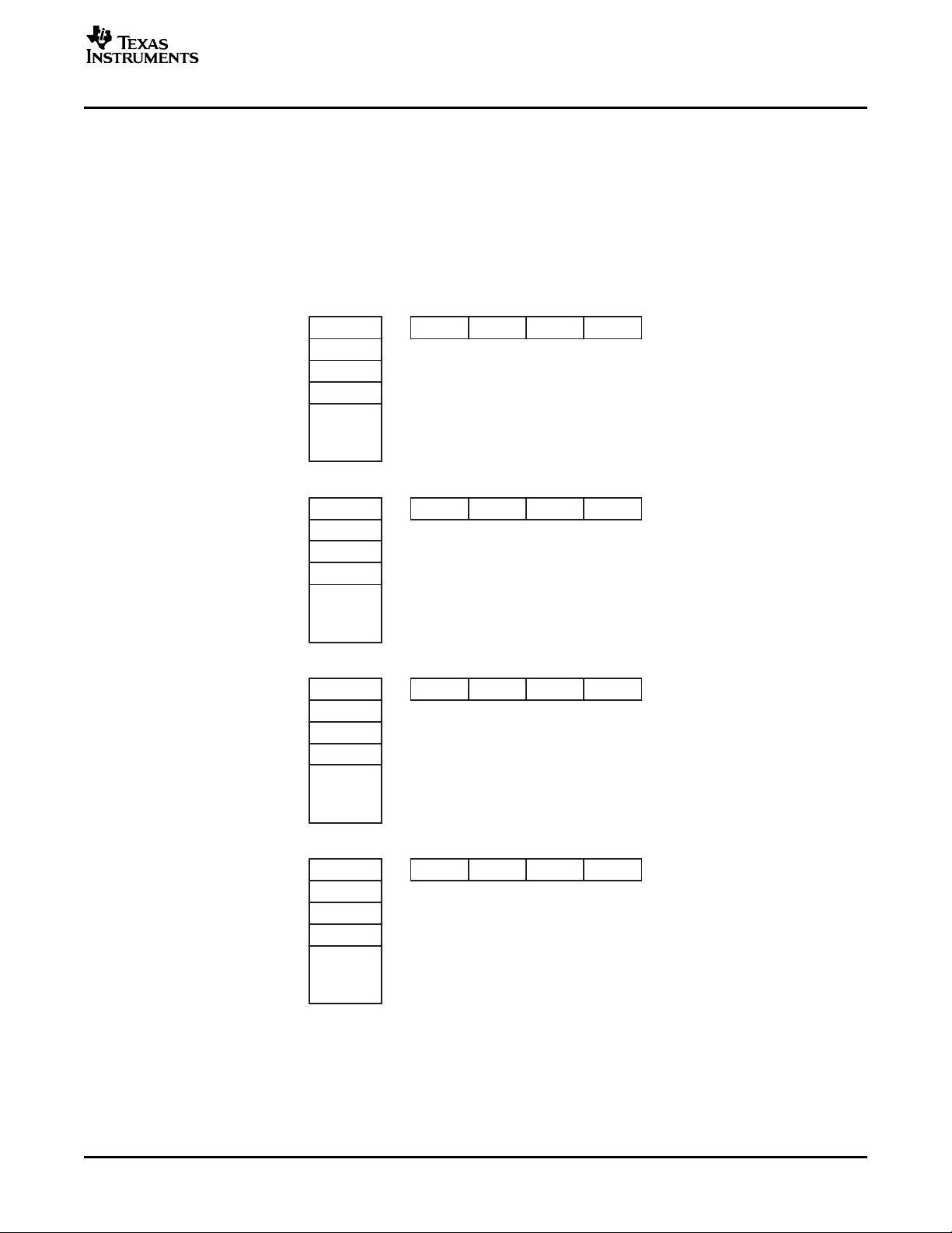
18 MMC Control Register (MMCCTL) ....................................................................................... 41
19 MMC Memory Clock Control Register (MMCCLK) ..................................................................... 42
20 MMC Status Register 0 (MMCST0) ...................................................................................... 43
21 MMC Status Register 1 (MMCST1) ...................................................................................... 45
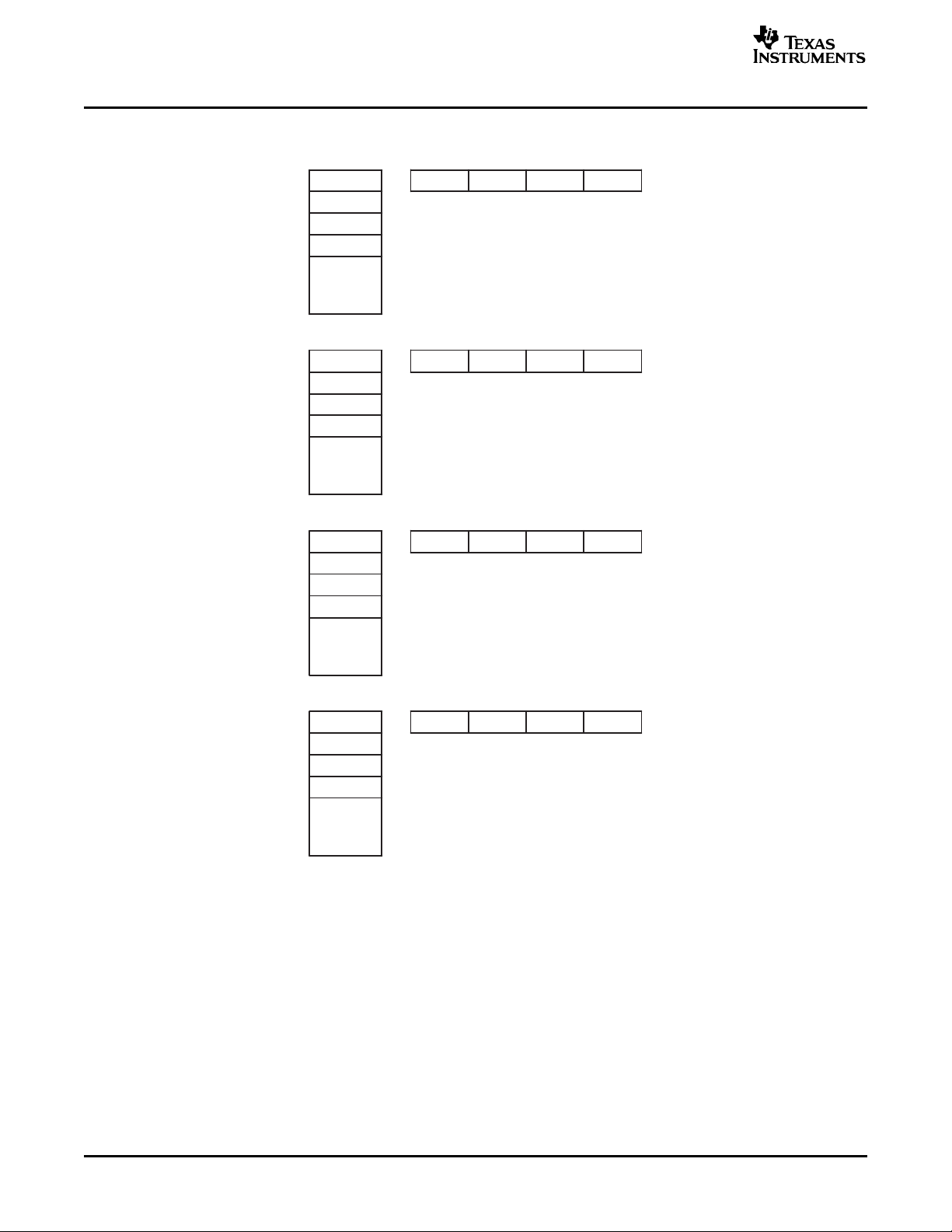
22 MMC Interrupt Mask Register (MMCIM) ................................................................................ 46
23 MMC Response Time-Out Register (MMCTOR) ....................................................................... 47
24 MMC Data Read Time-Out Register (MMCTOD) ...................................................................... 48
25 MMC Block Length Register (MMCBLEN) .............................................................................. 49
26 MMC Number of Blocks Register (MMCNBLK) ........................................................................ 50
27 MMC Number of Blocks Counter Register (MMCNBLC) .............................................................. 50
28 MMC Data Receive Register (MMCDRR)............................................................................... 51
29 MMC Data Transmit Register (MMCDXR) .............................................................................. 51
30 MMC Command Register (MMCCMD) .................................................................................. 52
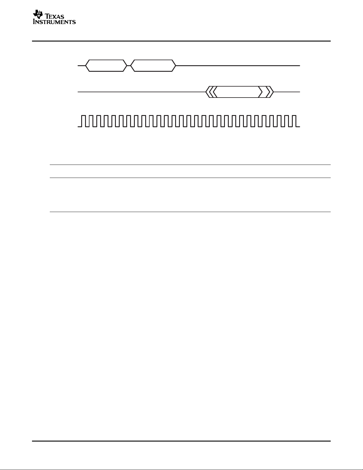
31 Command Format .......................................................................................................... 53
32 MMC Argument Register (MMCARGHL) ................................................................................ 54
33 MMC Response Register 0 and 1 (MMCRSP01) ...................................................................... 55
34 MMC Response Register 2 and 3 (MMCRSP23) ...................................................................... 55
35 MMC Response Register 4 and 5 (MMCRSP45) ...................................................................... 55
36 MMC Response Register 6 and 7 (MMCRSP67) ...................................................................... 55
37 MMC Data Response Register (MMCDRSP) .......................................................................... 57
38 MMC Command Index Register (MMCCIDX) .......................................................................... 57
39 MMC FIFO Control Register (MMCFIFOCTL) .......................................................................... 58
SPRUE30B – September 2006 List of Figures 5
Submit Documentation Feedback
Page 6

List of Tables
1 MMC/SD Controller Pins Used in Each Mode .......................................................................... 13
2 MMC/SD Mode Write Sequence ......................................................................................... 14
3 MMC/SD Mode Read Sequence ......................................................................................... 15
4 Description of MMC/SD Interrupt Requests ............................................................................ 27
5 Multimedia Card/Secure Digital (MMC/SD) Card Controller Registers .............................................. 40
6 MMC Control Register (MMCCTL) Field Descriptions................................................................. 41
7 MMC Memory Clock Control Register (MMCCLK) Field Descriptions .............................................. 42
8 MMC Status Register 0 (MMCST0) Field Descriptions ............................................................... 43
9 MMC Status Register 1 (MMCST1) Field Descriptions ............................................................... 45
10 MMC Interrupt Mask Register (MMCIM) Field Descriptions .......................................................... 46
11 MMC Response Time-Out Register (MMCTOR) Field Descriptions ................................................ 47
12 MMC Data Read Time-Out Register (MMCTOD) Field Descriptions ................................................ 48
13 MMC Block Length Register (MMCBLEN) Field Descriptions ........................................................ 49
14 MMC Number of Blocks Register (MMCNBLK) Field Descriptions .................................................. 50
15 MMC Number of Blocks Counter Register (MMCNBLC) Field Descriptions ....................................... 50
16 MMC Data Receive Register (MMCDRR) Field Descriptions ........................................................ 51
17 MMC Data Transmit Register (MMCDXR) Field Descriptions ........................................................ 51
18 MMC Command Register (MMCCMD) Field Descriptions ............................................................ 52
19 Command Format .......................................................................................................... 53
20 MMC Argument Register (MMCARGHL) Field Descriptions ......................................................... 54
21 R1, R3, R4, R5, or R6 Response (48 Bits) ............................................................................. 56
22 R2 Response (136 Bits) ................................................................................................... 56
23 MMC Data Response Register (MMCDRSP) Field Descriptions .................................................... 57
24 MMC Command Index Register (MMCCIDX) Field Descriptions .................................................... 57
25 MMC FIFO Control Register (MMCFIFOCTL) Field Descriptions ................................................... 58
A-1 Document Revision History ............................................................................................... 59
6 List of Tables SPRUE30B – September 2006
Submit Documentation Feedback
Page 7

About This Manual
Notational Conventions
Preface
SPRUE30B – September 2006
Read This First
This manual describes the multimedia card (MMC)/secure digital (SD) card controller in the
TMS320DM644x Digital Media System-on-Chip (DMSoC). The MMC/SD card is used in a number of
applications to provide removable data storage. The MMC/SD controller provides an interface to external
MMC and SD cards. The MMC/SD protocol performs the communication between the MMC/SD controller
and MMC/SD card(s).
This document uses the following conventions.
• Hexadecimal numbers are shown with the suffix h. For example, the following number is 40
hexadecimal (decimal 64): 40h.
• Registers in this document are shown in figures and described in tables.
– Each register figure shows a rectangle divided into fields that represent the fields of the register.
Each field is labeled with its bit name, its beginning and ending bit numbers above, and its
read/write properties below. A legend explains the notation used for the properties.
– Reserved bits in a register figure designate a bit that is used for future device expansion.
Related Documentation From Texas Instruments
The following documents describe the TMS320DM644x Digital Media System-on-Chip (DMSoC). Copies
of these documents are available on the Internet at www.ti.com . Tip: Enter the literature number in the
search box provided at www.ti.com.
The current documentation that describes the DM644x DMSoC, related peripherals, and other technical
collateral, is available in the C6000 DSP product folder at: www.ti.com/c6000 .
SPRUE14 — TMS320DM644x DMSoC ARM Subsystem Reference Guide. Describes the ARM
subsytem in the TMS320DM644x Digital Media System-on-Chip (DMSoC). The ARM subsystem is
designed to give the ARM926EJ-S (ARM9) master control of the device. In general, the ARM is
responsible for configuration and control of the device; including the DSP subsystem, the video
processing subsystem, and a majority of the peripherals and external memories.
SPRUE15 — TMS320DM644x DMSoC DSP Subsystem Reference Guide. Describes the digital signal
processor (DSP) subsystem in the TMS320DM644x Digital Media System-on-Chip (DMSoC).
SPRUE19 — TMS320DM644x DMSoC Peripherals Overview Reference Guide. Provides an overview
and briefly describes the peripherals available on the TMS320DM644x Digital Media
System-on-Chip (DMSoC).
SPRAA84 — TMS320C64x to TMS320C64x+ CPU Migration Guide. Describes migrating from the
Texas Instruments TMS320C64x digital signal processor (DSP) to the TMS320C64x+ DSP. The
objective of this document is to indicate differences between the two cores. Functionality in the
devices that is identical is not included.
SPRU732 — TMS320C64x/C64x+ DSP CPU and Instruction Set Reference Guide. Describes the CPU
architecture, pipeline, instruction set, and interrupts for the TMS320C64x and TMS320C64x+ digital
signal processors (DSPs) of the TMS320C6000 DSP family. The C64x/C64x+ DSP generation
comprises fixed-point devices in the C6000 DSP platform. The C64x+ DSP is an enhancement of
the C64x DSP with added functionality and an expanded instruction set.
SPRUE30B – September 2006 Preface 7
Submit Documentation Feedback
Page 8

www.ti.com
Related Documentation From Texas Instruments
SPRU871 — TMS320C64x+ DSP Megamodule Reference Guide. Describes the TMS320C64x+ digital
signal processor (DSP) megamodule. Included is a discussion on the internal direct memory access
(IDMA) controller, the interrupt controller, the power-down controller, memory protection, bandwidth
management, and the memory and cache.
SPRAAA6 — EDMA v3.0 (EDMA3) Migration Guide for TMS320DM644x DMSoC. Describes migrating
from the Texas Instruments TMS320C64x digital signal processor (DSP) enhanced direct memory
access (EDMA2) to the TMS320DM644x Digital Media System-on-Chip (DMSoC) EDMA3. This
document summarizes the key differences between the EDMA3 and the EDMA2 and provides
guidance for migrating from EDMA2 to EDMA3.
Trademarks
SD is a trademark of SanDisk.
8 Read This First SPRUE30B – September 2006
Submit Documentation Feedback
Page 9

1 Introduction
This document describes the multimedia card (MMC)/secure digital (SD) card controller in the
TMS320DM644x Digital Media System-on-Chip (DMSoC).
1.1 Purpose of the Peripheral
A number of applications use the multimedia card (MMC)/secure digital (SD) card to provide removable
data storage. The MMC/SD card controller provides an interface to external MMC and SD cards. The
communication between the MMC/SD card controller and MMC/SD card(s) is performed according to the
MMC/SD protocol.
1.2 Features
The MMC/SD card controller has the following features:
• Supports interface to multimedia cards (MMC)
• Supports interface to secure digital (SD) memory cards
• Ability to use the MMC/SD protocol
• Programmable frequency of the clock that controls the timing of transfers between the MMC/SD
controller and memory card
• 256-bit read/write FIFO to lower system overhead
• Signaling to support enhanced direct memory access (EDMA) transfers (slave)
• 20 MHz maximum clock to MMC (specification 3.31)
• 50 MHz maximum clock to SD (specification version 1.1)
User's Guide
SPRUE30B – September 2006
Multimedia Card (MMC)/Secure Digital (SD) Card
Controller
1.3 Functional Block Diagram
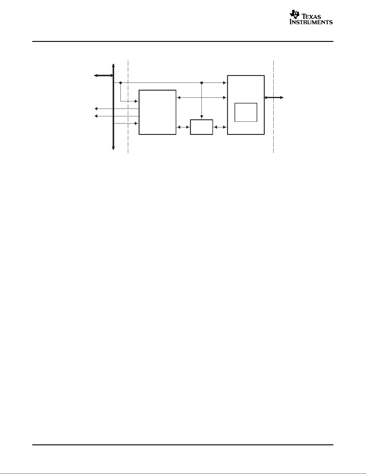
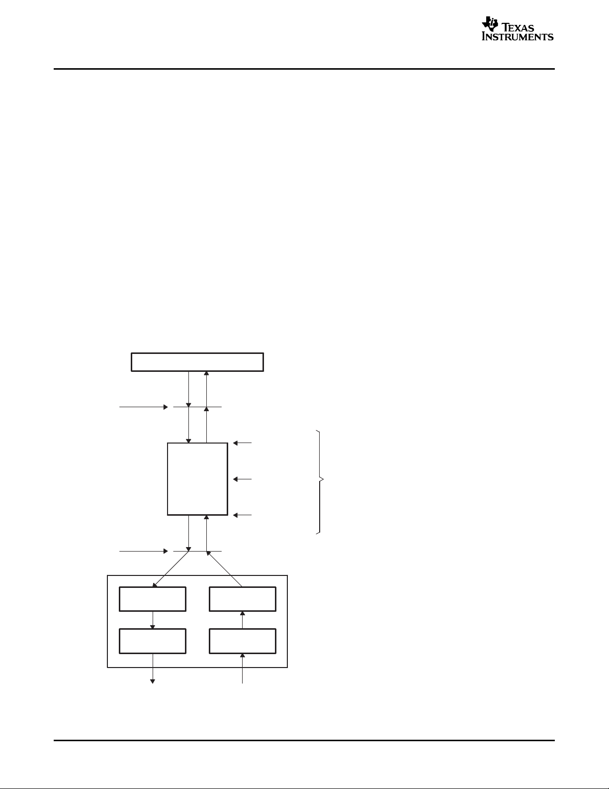
The MMC/SD card controller transfers data between the ARM and the EDMA controller on one side and
the MMC/SD card on the other side, as shown in Figure 1 . This means you have a choice of performing
data transfers using the CPU or EDMA as a mechanism to move data between the device memory and
the FIFO. The ARM and the EDMA controller can read from or write to the data in the card by accessing
the registers in the MMC/SD controller.
SPRUE30B – September 2006 Multimedia Card (MMC)/Secure Digital (SD) Card Controller 9
Submit Documentation Feedback
Page 10
www.ti.com
Status
and
registers
DMA requests
Interrupts
ARM CPU
FIFO
MMC/SD
interface
CLK
divider
MMC/SD
card
interface
Peripheral Architecture
1.4 Supported Use Case Statement
The MMC/SD card controller supports the following user cases:
• MMC/SD card identification
• MMC/SD single-block read using CPU
• MMC/SD single-block read using EDMA
• MMC/SD single-block write using CPU
• MMC/SD single-block write using EDMA
• MMC/SD multiple-block read using CPU
• MMC/SD multiple-block read using EDMA
• MMC/SD multiple-block write using CPU
• MMC/SD multiple-block write using EDMA
Figure 1. MMC/SD Card Controller Block Diagram
1.5 Industry Standard(s) Compliance Statement
The MMC/SD card controller supports the following industry standards (with the exception noted below):
• MMC (Multimedia Card) Specification V3.31
• SD (Secure Digital) Physical Layer Specification V1.1
The information in this document assumes that you are familiar with these standards.
The MMC/SD controller does not support the SPI mode of operation.
2 Peripheral Architecture
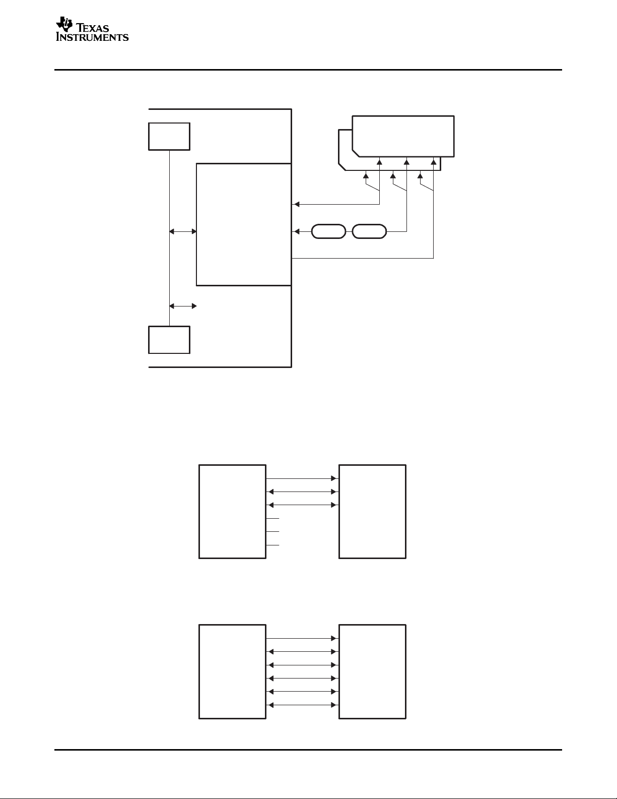
The MMC/SD controller uses the MMC/SD protocol to communicate with the MMC/SD cards. You can
configure the MMC/SD controller to work as an MMC or SD controller, based on the type of card the
controller is communicating with. Figure 2 summarizes the MMC/SD mode interface. Figure 3 illustrates
how the controller interfaces to the cards in MMC/SD mode.
In the MMC/SD mode, the MMC controller supports one or more MMC/SD cards. Regardless of the
number of cards connected, the MMC/SD controller selects one by using identification broadcast on the
data line. The following MMC/SD controller pins are used:
• CMD: This pin is used for two-way communication between the connected card and the MMC/SD
controller. The MMC/SD controller transmits commands to the card and the memory card drives
responses to the commands on this pin.
• DAT0 or DAT0-3: MMC cards only use one data line (DAT0) and SD cards use one or four data lines.
The number of DAT pins (the data bus width) is set by the WIDTH bit in the MMC control register
(MMCCTL), see Section 4.1 ).
• CLK: This pin provides the clock to the memory card from the MMC/SD controller.
10 Multimedia Card (MMC)/Secure Digital (SD) Card Controller SPRUE30B – September 2006
Submit Documentation Feedback
Page 11
www.ti.com
Native packets
Native
signals
CMD
CLK
DAT0 or DAT0−3
MMC/SD
controller
ARM
EDMA
Memory
MMCs or SD cards
SD_CLK
SD_CMD
SD_DATA0
SD_DATA1
SD_DATA2
SD_DATA3
MMC/SD controller MMC and SD (1−bit mode)
CLK
CMD
DAT0
MMC/SD configuration
MMC/SD controller
SD_DATA0
SD_CMD
SD_CLK
DAT0
CMD
SD card (4−bit mode)
CLK
SD_DATA2
SD_DATA3
SD_DATA1
SD configuration
DAT1
DAT2
DAT3
Figure 2. MMC/SD Controller Interface Diagram
Peripheral Architecture
Figure 3. MMC Configuration and SD Configuration Diagram
SPRUE30B – September 2006 Multimedia Card (MMC)/Secure Digital (SD) Card Controller 11
Submit Documentation Feedback
Page 12
www.ti.com
MMCCLK
(CLKRT)
Function clock for
MMC/SD controller
MMC/SD controller
MMC/SD
input clock
card
MMC/SD
Memory clock
on CLK pin
Peripheral Architecture
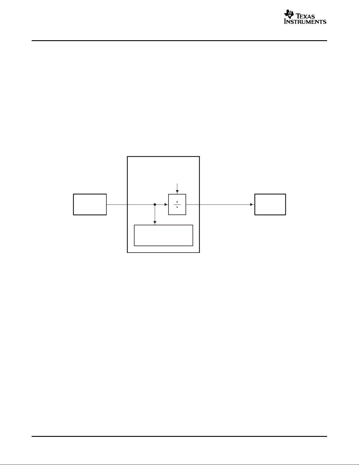
2.1 Clock Control
There are two clocks, the function clock and the memory clock, in the MMC/SD controller (Figure 4 ).
The function clock determines the operational frequency of the MMC/SD controller and is the input clock
to the MMC/SD card(s). The MMC/SD controller is capable of operating with a function clock up to
100 MHz.
The memory clock appears on the SD_CLK pin of the MMC/SD controller interface. The memory clock
controls the timing of communication between the MMC/SD controller and the connected memory card.
The memory clock is generated by dividing the function clock in the MMC/SD controller. The divide-down
value is set by CLKRT bits in the MMC memory clock control register (MMCCLK) and is determined by the
following equation:
memory clock frequency = function clock frequency/(2 × (CLKRT + 1))
Figure 4. MMC/SD Controller Clocking Diagram
(1) Maximum memory clock frequency in MMC card can be 20 MHz.
(2) Maximum memory clock frequency in SD card can be 50 MHz.
Multimedia Card (MMC)/Secure Digital (SD) Card Controller12 SPRUE30B – September 2006
Submit Documentation Feedback
Page 13
www.ti.com
2.2 Signal Descriptions
2.3 Protocol Descriptions
Peripheral Architecture
Table 1 shows the MMC/SD controller pins that each mode uses. The MMC/SD protocol uses the clock,
command (two-way communication between the MMC controller and memory card), and data (DAT0 for
MMC card, DAT0-3 for SD card) pins.
Table 1. MMC/SD Controller Pins Used in Each Mode
Function
Pin Type
CLK O Clock line Clock line
CMD I/O Command line Command line
DAT0 I/O Data line 0 Data line 0
DAT1 I/O (Not used) Data line 1
DAT2 I/O (Not used) Data line 2
DAT3 I/O (Not used) Data line 3
(1)
I = input to the MMC controller; O = output from the MMC controller.
(1)
MMC and SD (1-bit mode) SD (4-bit mode)
Communications Communications
The MMC/SD controller follows the MMC/SD protocol for completing any kind of transaction with the
multimedia card and secure digital cards. For more detailed information, refer to the supported MMC and
SD specifications in Section 1.5 .
2.3.1 MMC/SD Mode Write Sequence
Figure 5 and Table 2 show the signal activity when the MMC/SD controller is in the MMC/SD mode and is
writing data to a memory card. The same block length must be defined in the MMC/SD controller and in
the memory card before initiating a data write. In a successful write protocol sequence, the following steps
occur:
• The MMC/SD controller requests the CSD content.
• The card receives the command and sends the content of the CSD register as its response.
• If the desired block length, WRITE_BL_LEN value, is different from the default value determined from
the response, the MMC/SD controller sends the block length command.
• The card receives the command and sends responses to the command.
• The MMC/SD controller requests the card to change states from standby to transfer.
• The card receives the command and sends responses to the command.
• The MMC/SD controller sends a write command to the card.
• The card receives the command and sends responses to the command.
• The MMC/SD controller sends a block of data to the card.
• The card sends the CRC status to the MMC/SD controller.
• The card sends a low BUSY bit until all of the data has been programmed into the flash memory inside
the card.
SPRUE30B – September 2006 Multimedia Card (MMC)/Secure Digital (SD) Card Controller 13
Submit Documentation Feedback
Page 14

www.ti.com
2 CRC bytes
Busy
low
Start
bit
End
bit
Start
bit
End
bit
CMD
Data
CLK
Peripheral Architecture
Figure 5. MMC/SD Mode Write Sequence Timing Diagram
Table 2. MMC/SD Mode Write Sequence
Portion of the
Sequence Description
WR CMD Write command: A 6-byte WRITE_BLOCK command token is sent from the ARM to the card.
CMD RSP Command response: The card sends a 6-byte response of type R1 to acknowledge the WRITE_BLOCK to the
DAT BLK Data block: The ARM writes a block of data to the card. The data content is preceded by one start bit and is
CRC STAT CRC status: The card sends a one byte CRC status information, which indicates to the ARM whether the data has
BSY BUSY bit: The CRC status information is followed by a continuous stream of low busy bits until all of the data has
ARM.
followed by two CRC bytes and one end bit.
been accepted by the card or rejected due to a CRC error. The CRC status information is preceded by one start
bit and is followed by one end bit.
been programmed into the flash memory on the card.
2.3.2 MMC/SD Mode Read Sequence
Figure 6 and Table 3 show the signal activity when the MMC controller is in the MMC/SD mode and is
reading data from a memory card. The same block length must be defined in the MMC controller and in
the memory card before initiating a data read. In a successful read protocol sequence, the following steps
occur:
• The MMC/SD controller requests for the CSD content.
• The card receives the command and sends the content of the CSD register as its response.
• If the desired block length, READ_BL_LEN value, is different from the default value determined from
the response, the MMC/SD controller sends the block length command.
• The card receives the command and sends responses to the command.
• The MMC/SD controller requests the card to change state from stand-by to transfer.
• The card receives the command and sends responses to the command.
• The MMC/SD controller sends a read command to the card.
• The card drives responses to the command.
• The card sends a block of data to the ARM.
14 Multimedia Card (MMC)/Secure Digital (SD) Card Controller SPRUE30B – September 2006
Submit Documentation Feedback
Page 15
www.ti.com
Start
bit
End
bit
CMD
Data
CLK
1 transfer
source bit
2 CRC
bytes
Peripheral Architecture
Figure 6. MMC/SD Mode Read Sequence Timing Diagram
Table 3. MMC/SD Mode Read Sequence
Portion of the
Sequence Description
RD CMD Read command: A 6-byte READ_SINGLE_BLOCK command token is sent from the ARM to the card.
CMD RSP Command response: The card sends a response of type R1 to acknowledge the READ_SINGLE_BLOCK
DAT BLK Data block: The card sends a block of data to the ARM. The data content is preceded by a start bit and is
command to the ARM.
followed by two CRC byte and an end bit.
2.4 Data Flow in the Input/Output FIFO
The MMC/SD controller contains a single 256-bit FIFO that is used for both reading data from the memory
card and writing data to the memory card (see Figure 7 ). The FIFO is organized as 32 eight-bit entries.
The conversion from the 32-bit bus to the byte format of the FIFO follows the little-endian convention
(details are provided in later sections). The read and write FIFOs act as an interim location to store data
transferred from/to the card momentarily via the CPU or EDMA. The FIFO includes logic to generate
EDMA events and interrupts based on the amount of data in the FIFO and a programmable number of
bytes received/transmitted. Flags are set when the FIFO is full or empty.
SPRUE30B – September 2006 Multimedia Card (MMC)/Secure Digital (SD) Card Controller 15
Submit Documentation Feedback
Page 16
www.ti.com
ARM/EDMA reads/writes
Write Read
FIFO
8−bit x 32
(256−bit)
FIFO
EDMA event
128 or 256 bit
128 or 256 bit
EDMA event
EDMA event
the end of a
transfer
Pointer increment
or decrease
Pointer increment
or decrease
FIFO
16−bit DXR 16−bit DRR
16−bit DXR
shifter
16−bit DRR
shifter
DXR DRR
EDMA
request
is created
Transmission of data
Step 1: Set FIFO reset
Step 2: Set FIFO direction
Step 4: CPU driven transaction:
Fill the FIFO by writing to
MMCDXR (only first time)
Step 5: EDMA send xmit data
Step 6: If DXR ready is active,
FIFO −> 16−bit DXR
Reception of data
Step 3:
Step 2:
Step 1: Set FIFO reset
Set FIFO direction
If DRR ready is active,
16−bit DRR −> FIFO
Step 6: EDMA read reception data
Step 4: EDMA driven transaction
Step 5: DRRDYINT interrupt occur
Step 3: EDMA driven transaction
or every 128 or 256−bits
transmitted and DXRDYINT
interrupt is generated
when FIFO every 128 or
256−bits of data received
by FIFO
Peripheral Architecture
A high-level operational description is as follows:
• Data is written to the FIFO through the MMC data transmit register (MMCDXR). Data is read from the
FIFO through the MMC data receive register (MMCDRR). This is true for both the CPU and EDMA
driven transactions; however, for the EDMA transaction, the EDMA access to the FIFO is transparent.
• The ACCWD bits in the MMC FIFO control register (MMCFIFOCTL) determines the behavior of the
FIFO full (FIFOFUL) and FIFO empty (FIFOEMP) status flags in the MMC status register 1 (MMCST1):
– If ACCWD = 00b:
• FIFO full is active when the write pointer + 4 > read pointer
• FIFO empty is active when the write pointer - 4 < read pointer
– If ACCWD = 01b:
• FIFO full is active when the write pointer + 3 > read pointer
• FIFO empty is active when the write pointer - 3 < read pointer
– If ACCWD = 10b:
• FIFO full is active when the write pointer + 2 > read pointer
• FIFO empty is active when the write pointer - 2 < read pointer
– If ACCWD = 11b:
• FIFO full is active when the write pointer + 1 > read pointer
• FIFO empty is active when the write pointer - 1 < read pointer
Figure 7. FIFO Operation Diagram
Multimedia Card (MMC)/Secure Digital (SD) Card Controller16 SPRUE30B – September 2006
Submit Documentation Feedback
Page 17
www.ti.com
2.5 Data Flow in the Data Registers (MMCDRR and MMCDXR)
1st
2nd
3rd
4th
3
4th 3rd 2nd 1st
Support byten = ”1111”
Support byten = ”0111”
3rd
2nd
1st
3
3rd 2nd 1st
Support byten = ”0011”
1st
2nd
3
2nd 1st
0
Support byten = ”0001”
1st
3
1st
0
0
0
FIFO MMCDRR or MMCDXR registers
The CPU or EDMA controller can read 32 bits at a time from the FIFO by reading the MMC data receive
register (MMCDRR) and write 32 bits at a time to the FIFO by writing to the MMC data transmit register
(MMCDXR). However, since the memory card is an 8-bit device, it transmits or receives one byte at a
time. Figure 8 and Figure 9 show how the data-size difference is handled by the data registers in
little-endian and big-endian configurations, respectively.
Figure 8. Little-Endian Access to MMCDXR/MMCDRR from the ARM CPU or the EDMA
Peripheral Architecture
SPRUE30B – September 2006 Multimedia Card (MMC)/Secure Digital (SD) Card Controller 17
Submit Documentation Feedback
Page 18
www.ti.com
1st
2nd
3rd
4th
3
4th3rd2nd1st
Support byten = ”1111”
Support byten = ”1110”
3rd
2nd
1st
3
3rd2nd1st
Support byten = ”1100”
1st
2nd
3
2nd1st
0
Support byten = ”1000”
1st
3
1st
0
0
0
Peripheral Architecture
Figure 9. Big-Endian Access to MMCDXR/MMCDRR from the ARM CPU or the EDMA
18 Multimedia Card (MMC)/Secure Digital (SD) Card Controller SPRUE30B – September 2006
Submit Documentation Feedback
Page 19

www.ti.com
2.6 FIFO Operation During Card Read Operation
2.6.1 EDMA Reads
The FIFO controller manages the activities of reading the data in from the card and issuing EDMA read
events. Each time an EDMA read event is issued, an EDMA read request interrupt generates.
Figure 10 provides details of the FIFO controllers operation. As data is received from the card, it is read
into the FIFO. When the number of bytes of data received is equal to the level set by the FIFOLEV bits in
MMCFIFOCTL, an EDMA read event is issued and new EDMA events are disabled until the EDMA is
done with the transfer issued by the current event. Data is read from the FIFO by way of MMCDRR. The
FIFO controller continues to read in data from the card while checking for the EDMA event to occur or for
the FIFO to become full. Once the EDMA event finishes, new EDMA events are enabled. If the FIFO fills
up, the FIFO controller stops the MMC/SD controller from reading any more data until the FIFO is no
longer full.
An EDMA read event generates when the last data arrives, as determined by the MMC block length
register (MMCBLEN) and the MMC number of blocks register (MMCNBLK) settings. This EDMA event
flushes all of the data that was read from the card from the FIFO.
Each time an EDMA read event generates, an interrupt (DRRDYINT) generates and the DRRDY bit in the
MMC status register 0 (MMCST0) is also set.
2.6.2 CPU Reads
The system CPU can also directly read the card data by reading the MMC data receive register
(MMCDRR). The MMC/SD peripheral supports reads that are 1, 2, 3, or 4 bytes wide as, shown in
Figure 8 and Figure 9 .
As data is received from the card, it is read into the FIFO. When the number of bytes of data received is
equal to the level set by the FIFOLEV bits in MMCFIFOCTL, a DRRDYINT interrupt is issued and the
DRRDY bit in the MMC status register 0 (MMCST0) is set. Upon receiving the interrupt, the CPU quickly
reads out the bytes received (equal to the level set by the FIFOLEV bits). A DRRDYINT interrupt also
generates when the last data arrives as determined by the MMC block length register (MMCBLEN) and
the MMC numbers of blocks register (MMCNBLK) settings.
Peripheral Architecture
SPRUE30B – September 2006 Multimedia Card (MMC)/Secure Digital (SD) Card Controller 19
Submit Documentation Feedback
Page 20

www.ti.com
FIFO Check1/Start
FIFO
full
?
Counter
=FIFOLEV
?
Yes
No
Capture data,
no DMA pending
Increment counter
No
Yes
Generate DMA
Reset counter
FIFO check 2
Yes
No
?
full
FIFO
No
=FIFOLEV
?
Counter
Increment counter
DMA
Capture data,
done
?
DMA
No
Yes
Yes
Yes
Generate DMA
Reset counter
Idle, DMA pending
DMA
No
done
?
Peripheral Architecture
Figure 10. FIFO Operation During Card Read Diagram
Multimedia Card (MMC)/Secure Digital (SD) Card Controller20 SPRUE30B – September 2006
Submit Documentation Feedback
Page 21

www.ti.com
2.7 FIFO Operation During Card Write Operation
2.7.1 EDMA Writes
The FIFO controller manages the activities of accepting data from the CPU or EDMA and passing the data
to the MMC/SD controller. The FIFO controller issues EDMA write events as appropriate. Each time an
EDMA write event is issued, an EDMA write request interrupt generates. Data is written into the FIFO
through MMCDXR. Note that the EDMA access to MMCDXR is transparent.
Figure 11 provides details of the FIFO controller's operation. The CPU or EDMA controller writes data into
the FIFO. The FIFO passes the data to the MMC/SD controller which manages writing the data to the
card. When the number of bytes of data in the FIFO is less than the level set by the FIFOLEV bits in
MMCFIFOCTL, an EDMA write event is issued and new EDMA events are disabled. The FIFO controller
continues to transfer data to the MMC/SD controller while checking for the EDMA event to finish or for the
FIFO to become empty. Once the EDMA event finishes, new EDMA events are enabled. If the FIFO
becomes empty, the FIFO controller informs the MMC/SD controller.
Each time an EDMA write event generates, an interrupt (DXRDYINT) generates and the DXRDY bit in the
MMC status register 0 (MMCST0) is also set.
2.7.2 CPU Writes
The system CPU can also directly write the card data by writing the MMC data transmit register
(MMCDXR). The MMC/SD peripheral supports writes that are 1, 2, 3, or 4 bytes wide, as shown in
Figure 8 and Figure 9 .
The CPU makes use of the FIFO to transfer data to the card via the MMC/SD controller. The CPU writes
the data to be transferred into MMCDXR. As is the case with the EDMA driven transaction, when the
number of data in the FIFO is less than the level set by the FIFOLEV bits in MMCFIFOCTL, a DXRDYINT
interrupt generates and the DXRDY bit in the MMC status register 0 (MMCST0) is set to signify to the
CPU that space is available for new data.
Peripheral Architecture
Note: When starting the write transaction, the CPU is responsible for getting the FIFO ready to
start transferring data by filling up the FIFO with data prior to invoking/posting the write
command to the card. Filling up the FIFO is a requirement since no interrupt/event
generates at the start of the write transfer.
SPRUE30B – September 2006 Multimedia Card (MMC)/Secure Digital (SD) Card Controller 21
Submit Documentation Feedback
Page 22

www.ti.com
FIFO Check1/Start
FIFO
full
?
Counter
=FIFOLEV
?
Yes
No
Capture data,
no DMA pending
Increment counter
No
Yes
Generate DMA
Reset counter
FIFO check 2
Yes
No
?
full
FIFO
No
=FIFOLEV
?
Counter
Increment counter
DMA
Capture data,
done
?
DMA
No
Yes
Yes
Yes
Generate DMA
Reset counter
Idle, DMA pending
DMA
No
done
?
Peripheral Architecture
Figure 11. FIFO Operation During Card Write Diagram
Multimedia Card (MMC)/Secure Digital (SD) Card Controller22 SPRUE30B – September 2006
Submit Documentation Feedback
Page 23

www.ti.com
2.8 Reset Considerations
The MMC/SD peripheral has two reset sources: hardware reset and software reset.
2.8.1 Software Reset Considerations
A software reset (such as a reset that the emulator generates) does not cause the MMC/SD controller
registers to alter. After a software reset, the MMC/SD controller continues to operate as it was configured
prior to the reset.
2.8.2 Hardware Reset Considerations
A hardware reset of the processor causes the MMC/SD controller registers to return to their default values
after reset.
2.9 Initialization
2.9.1 MMC/SD Controller Initialization
The general procedure for initializing the MMC/SD controller is given in the following steps. Details about
the registers or register bit fields to be configured in the MMC/SD mode are in the subsequent
subsections.
1. Place the MMC/SD controller in its reset state by setting the CMDRST bit and DATRST bit in the MMC
control register (MMCCTL). You can set other bits in MMCCTL after reset.
2. Write the required values to other registers to complete the MMC/SD controller configuration.
3. Clear the CMDRST bit and the DATRST bit in MMCCTL to release the MMC/SD controller from its
reset state. It is recommended not to rewrite the values that are written to the other bits of MMCCTL in
Step 1 .
4. Enable the SD_CLK pin so that the memory clock is sent to the memory card by setting the CLKEN bit
in the MMC memory clock control register (MMCCLK).
Peripheral Architecture
Note: The MMC/SD cards require a clock frequency of 400 kHz or less for the card initialization
procedure. Make sure that the memory clock confirms this requirement. Once card
initialization completes, you can adjust the memory clock up to the lower of the card
capabilities or the maximum frequency that is supported.
2.9.2 Initializing the MMC Control Register (MMCCTL)
The bits in the MMC control register (MMCCTL) affect the operation of the MMC/SD controller. The
subsections that follow help you decide how to initialize each of control register bits.
In the MMC/SD mode, the MMC/SD controller must know how wide the data bus must be for the memory
card that is connected. If an MMC card is connected, specify a 1-bit data bus (WIDTH = 0 in MMCCTL); if
an SD card is connected, specify a 4-bit data bus (WIDTH = 1 in MMCCTL).
To place the MMC/SD controller in its reset state and disable it, set the CMDRST bit and DATRST bit in
MMCCTL. The first step of the MMC/SD controller initialization process is to disable both sets of logic.
When initialization is complete, but before you enable the SD_CLK pin, clear the CMDRST bit and
DATRST bit in MMCCTL to enable the MMC/SD controller.
SPRUE30B – September 2006 Multimedia Card (MMC)/Secure Digital (SD) Card Controller 23
Submit Documentation Feedback
Page 24

www.ti.com
Peripheral Architecture
2.9.3 Initializing the Clock Controller Registers (MMCCLK)
A clock divider in the MMC/SD controller divides-down the function clock to produce the memory clock.
Load the divide-down value into the CLKRT bits in the MMC memory clock control register (MMCCLK).
The divide-down value is determined by the following equation:
memory clock frequency = function clock frequency/(2 × (CLKRT + 1))
The CLKEN bit in MMCCLK determines whether the memory clock appears on the SD_CLK pin. If you
clear the CLKEN to 0, the memory clock is not provided except when required.
2.9.4 Initialize the Interrupt Mask Register (MMCIM)
The bits in the MMC interrupt mask register (MMCIM) individually enable or disable the interrupt requests.
To enable the associated interrupt request, set the corresponding bit in MMCIM. To disable the associated
interrupt request, clear the corresponding bit. Load zeros into the bits that are not used in the MMC/SD
mode.
2.9.5 Initialize the Time-Out Registers (MMCTOR and MMCTOD)
Specify the time-out period for responses using the MMC response time-out register (MMCTOR) and the
time-out period for reading data using the MMC data read time-out register (MMCTOD).
When the MMC/SD controller sends a command to a memory card, it must often wait for a response. The
MMC/SD controller can wait indefinitely or up to 255 memory clock cycles. If you load 0 into MMCTOR,
the MMC/SD controller waits indefinitely for a response. If you load a nonzero value into MMCTOR, the
MMC/SD controller stops waiting after the specified number of memory clock cycles and then sets a
response time-out flag (TOUTRS) in the MMC status register 0 (MMCST0). If you enable the associated
interrupt request, the MMC/SD controller also sends an interrupt request to the ARM.
When the MMC/SD controller requests data from a memory card, it can wait indefinitely for that data or it
can stop waiting after a programmable number of cycles. If you load 0 into MMCTOD, the MMC/SD
controller waits indefinitely. If you load a nonzero value into MMCTOD, the MMC/SD controller waits the
specified number of memory clock cycles and then sets a read data time-out flag (TOUTRD) in MMCST0.
If you enable the associated interrupt request, the MMC/SD controller also sends an interrupt request to
the ARM.
2.9.6 Initialize the Data Block Registers (MMCBLEN and MMCNBLK)
Specify the number of bytes in a data block in the MMC block length register (MMCBLEN) and the number
of blocks in a multiple-block transfer in the MMC number of blocks register (MMCNBLK).
You must define the size for each block of data transferred between the MMC/SD controller and a memory
card in MMCBLEN. The valid size depends on the type of read/write operations. A length of 0 bytes is
prohibited.
For multiple-block transfers, you must specify how many blocks of data are to be transferred between the
MMC/SD controller and a memory card. You can specify an infinite number of blocks by loading 0 into
MMCNBLK. When MMCNBLK = 0, the MMC/SD controller continues to transfer data blocks until the
transferring is stopped with a STOP_TRANSMISSION command. To transfer a specific number of blocks,
load MMCNBLK with a value from 1 to 65 535.
Multimedia Card (MMC)/Secure Digital (SD) Card Controller24 SPRUE30B – September 2006
Submit Documentation Feedback
Page 25

www.ti.com
2.9.7 Monitoring Activity in the MMC/SD Mode
This section describes registers and specific register bits that you can use to obtain the status of the
MMC/SD controller in the MMC/SD mode. You can determine the status of the MMC/SD controller by
reading the bits in the MMC status register 0 (MMCST0) and MMC status register 1 (MMCST1).
2.9.7.1 Determining Whether New Data is Available in MMCDRR
The MMC/SD controller sets the DRRDY bit in MMCST0 when the data in the FIFO is greater than the
threshold set in the MMC FIFO control register (MMCFIFOCTL). If the interrupt request is enabled
(EDRRDY = 1 in MMCIM), the ARM is notified of the event by an interrupt. A read of the MMC data
receive register (MMCDDR) clears the DRRDY flag.
2.9.7.2 Verifying that MMCDXR is Ready to Accept New Data
The MMC/SD controller sets the DXRDY bit in MMCST0 when the amount of data in the FIFO is less than
the threshold set in the MMC FIFO control register (MMCFIFOCTL). If the interrupt request is enabled
(EDXRDY = 1 in MMCIM), the ARM is notified of the event by an interrupt.
2.9.7.3 Checking for CRC Errors
The MMC/SD controller sets the CRCRS, CRCRD, and CRCWR bits in MMCST0 in response to the
corresponding CRC errors of command response, data read, and data write. If the interrupt request is
enabled (ECRCRS/ECRCRD/ECRCWR = 1 in MMCIM), the ARM is notified of the CRC error by an
interrupt.
Peripheral Architecture
2.9.7.4 Checking for Time-Out Events
The MMC/SD controller sets the TOUTRS and TOUTRD bits in MMCST0 in response to the
corresponding command response or data read time-out event. If the interrupt request is enabled
(ETOUTRS/ETOUTRD = 1 in MMCIM), the ARM is notified of the event by an interrupt.
2.9.7.5 Determining When a Response/Command is Done
The MMC/SD controller sets the RSPDNE bit in MMCST0 when the response is done; or in the case of
commands that do not require a response, when the command is done. If the interrupt request is enabled
(ERSPDNE = 1 in MMCIM), the ARM is also notified.
2.9.7.6 Determining Whether the Memory Card is Busy
The card sends a busy signal either when waiting for an R1b-type response or when programming the last
write data into its flash memory. The MMC/SD controller has two flags to notify you whether the memory
card is sending a busy signal. The two flags are complements of each other:
• The BSYDNE flag in MMCST0 is set if the card did not send or is not sending a busy signal when the
MMC/SD controller is expecting a busy signal (BSYEXP = 1 in MMCCMD). The interrupt by this bit is
enabled by a corresponding interrupt enable bit (EBSYDNE = 1 in MMCIM).
• The BUSY flag in MMCST1 is set when a busy signal is received from the card.
2.9.7.7 Determining Whether a Data Transfer is Done
The MMC/SD controller sets the DATDNE bit in MMCST0 when all of the bytes of a data transfer have
been transmitted/received. The DATDNE bit is polled to determine when to stop writing to the data
transmit register (for a write operation) or when to stop reading from the data receive register (for a read
operation). The ARM is also notified of the time-out event by an interrupt if the interrupt request is enabled
(EDATDNE = 1 in MMCIM).
SPRUE30B – September 2006 Multimedia Card (MMC)/Secure Digital (SD) Card Controller 25
Submit Documentation Feedback
Page 26

www.ti.com
Peripheral Architecture
2.9.7.8 Determining When Last Data has Been Written to Card (SanDisk SD cards)
Some SanDisk brand SD™ cards exhibit a behavior that requires a multiple-block write command to
terminate with a STOP (CMD12) command before the data write sequence completes. To enable support
of this function, the transfer done interrupt (TRNDNE) is provided. Set the ETRNDNE bit in MMCIM to
enable the TRNDNE interrupt. This interrupt is issued when the last byte of data (as defined by
MMCNBLK and MMCBLEN) is transferred from the FIFO to the output shift register. The CPU should
respond to this interrupt by sending a STOP command to the card. This interrupt differs from DATDNE by
timing. DATDNE does not occur until after the CRC and memory programming are complete.
2.9.7.9 Checking For a Data Transmit Empty Condition
During transmission, a data value is passed from the MMC data transmit register (MMCDXR) to the data
transmit shift register. The data is then passed from the shift register to the memory card one bit at a time.
The DXEMP bit in MMCST1 indicates when the shift register is empty.
Typically, the DXEMP bit is not used to control data transfers; rather, it is checked during recovery from an
error condition. There is no interrupt associated with the DXEMP bit.
2.9.7.10 Checking for a Data Receive Full Condition
During reception, the data receive shift register accepts a data value one bit at a time. The entire value is
then passed from the shift register to the MMC data receive register (MMCDRR). The DRFUL bit in
MMCST1 indicates that when the shift register is full no new bits can be shifted in from the memory card.
The DRFUL bit is not typically used to control data transfers; rather, it is checked during recovery from an
error condition. There is no interrupt associated with the DRFUL bit.
2.9.7.11 Checking the Status of the SD_CLK Pin
Read the CLKSTP bit in MMCST1 to determine whether the memory clock has been stopped on the
SD_CLK pin.
2.9.7.12 Checking the Remaining Block Count During a Multiple-Block Transfer
During a transfer of multiple data blocks, the MMC number of blocks counter register (MMCNBLC)
indicates how many blocks are remaining to be transferred. The MMCNBLC is a read-only register.
Multimedia Card (MMC)/Secure Digital (SD) Card Controller26 SPRUE30B – September 2006
Submit Documentation Feedback
Page 27

www.ti.com
2.10 Interrupt Support
2.10.1 Interrupt Events and Requests
The MMC/SD controller generates the interrupt requests described in Table 4 . When an interrupt event
occurs, its flag bit is set in the MMC status register 0 (MMCST0). If the enable bits corresponding to each
flag are set in the MMC interrupt mask register (MMCIM), an interrupt request generates. All such
requests are multiplexed to a single MMC/SD interrupt request from the MMC/SD peripheral to the ARM
CPU.
The MMC/SD interrupts are part of the maskable ARM interrupts. The ARM interrupt 26 (INT26) is
associated with MMC functions and the ARM interrupt 27 (INT27) is associated with SD functions. The
interrupt service routine (ISR) for the MMC/SD interrupt can determine the event that caused the interrupt
by checking the bits in MMCST0. When MMCST0 is read, all register bits automatically clear. During a
middle of data transfer, the DXRDY and DRRDY bits are set during every 128-byte or 256-byte transfer,
depending on the the MMC FIFO control register (MMCFIFOCTL) setting. Performing a write and a read in
response to the interrupt generated by the FIFO automatically clears the corresponding interrupt bit/flag.
Note: You must be aware that an emulation read of the status register clears the interrupt status
flags. To avoid inadvertently clearing the flag, be careful while monitoring MMCST0 via
the debugger.
2.10.2 Interrupt Multiplexing
The interrupts from the MMC/SD peripheral to the ARM CPU are not multiplexed with any other interrupt
source.
Peripheral Architecture
Table 4. Description of MMC/SD Interrupt Requests
Interrupt
Request Interrupt Event
TRNDNEINT For read operations: The MMC/SD controller has received the last byte of data (before CRC check).
For write operations: The MMC/SD controller has transferred the last word of data to the output shift register.
DATEDINT An edge was detected on the DAT3 pin.
DRRDYINT MMCDRR is ready to be read (data in FIFO is above threshold).
DXRDYINT MMCDXR is ready to transmit new data (data in FIFO is less than threshold).
CRCRSINT A CRC error was detected in a response from the memory card.
CRCRDINT A CRC error was detected in the data read from the memory card.
CRCWRINT A CRC error was detected in the data written to the memory card.
TOUTRSINT A time-out occurred while the MMC controller was waiting for a response to a command.
TOUTRDINT A time-out occurred while the MMC controller was waiting for the data from the memory card.
RSPDNEINT For a command that requires a response: The MMC controller has received the response without a CRC error.
For a command that does not require a response: The MMC controller has finished sending the command.
BSYDNEINT The memory card stops or is no longer sending a busy signal when the MMC controller is expecting a busy signal.
DATDNEINT For read operations: The MMC controller has received data without a CRC error.
For write operations: The MMC controller has finished sending data.
SPRUE30B – September 2006 Multimedia Card (MMC)/Secure Digital (SD) Card Controller 27
Submit Documentation Feedback
Page 28

www.ti.com
Peripheral Architecture
2.11 DMA Event Support
The MMC/SD controller is capable of generating EDMA events for both read and write operations in order
to request service from an EDMA controller. Based on the FIFO threshold setting, the EDMA event signals
generate every time 128-bit or 256-bit data is transferred from the FIFO.
2.12 Power Management
You can put the MMC/SD peripheral in reduced-power modes to conserve power during periods of low
activity. The processor power and sleep controller (PSC) controls the power management of the MMC/SD
peripheral. The PSC acts as a master controller for power management for all of the peripherals on the
device. For detailed information on power management procedures using the PSC, see the
TMS320DM644x DMSoC ARM Subsystem Reference Guide (SPRUE14 ).
2.13 Emulation Considerations
The MMC/SD peripheral is not affected by emulation halt events (such as breakpoints).
Multimedia Card (MMC)/Secure Digital (SD) Card Controller28 SPRUE30B – September 2006
Submit Documentation Feedback
Page 29

www.ti.com
3 Procedures for Common Operations
3.1 Card Identification Operation
Before the MMC/SD controller starts data transfers to or from memory cards in the MMC/SD native mode,
it must first identify how many cards are present on the bus and configure them. For each card that
responds to the ALL_SEND_CID broadcast command, the controller reads that card’s unique card
identification address (CID) and then assigns it a relative address (RCA). This address is much shorter
than the CID and the MMC/SD controller uses this address to identify the card in all future commands that
involve the card.
Only one card completes the response to ALL_SEND_CID at any one time. The absence of any response
to ALL_SEND_CID indicates that all cards have been identified and configured.
Note: The following steps assume that the MMC/SD controller is configured to operate in MMC
or SD mode, and the memory clock frequency on the CLK pin is set for 400 kHz or less.
The procedure for a card identification operation is issued in open-drain bus mode for both MMC and SD
cards.
3.1.1 MMC Card Identification Procedure
The MMC card identification procedure is:
1. Use the MMC command register (MMCCMD) to issue the GO_IDLE_STATE (CMD0) command to the
MMC cards. Using MMCCMD to issue the CMD0 command puts all cards (MMC and SD) in the idle
state and no response from the cards is expected.
2. Use MMCCMD to issue the SEND_OP_CMD (CMD1) command with the voltage range supported (R3
response, if it is successful; R1b response, if the card is expected to be busy). Using MMCCMD to
issue the CMD1 command allows the host to identify and reject cards that do not match the VDD
range that the host supports.
3. If the response in step 2 is R1b (that is, the card is still busy due to power up), then go back to step 2.
If the card is not busy, continue to step 4.
4. Use MMCCMD to send the ALL_SEND_CID (CMD2) command (R2 response is expected) to the MMC
cards. Using MMCCMD to send the CMD2 command notifies all cards to send their unique card
identification (CID) number. There should only be one card that successfully sends its full CID number
to the host. The successful card goes into the identification state and does not respond to this
command again.
5. Use MMCMD to issue the SET_RELATIVE_ADDR (CMD3) command (R1 response is expected) in
order to assign an address that is shorter than the CID number that will be used in the future to
address the card in the future data transfer mode.
Procedures for Common Operations
Note: This command is only addressed to the card that successfully sent its CID number in
step 4. This card now goes into standby mode. This card also changes its output drivers
from open-drain to push-pull. It stops replying to the CMD2 command, allowing for the
identification of other cards.
6. Repeat step 4 and step 5 to identify and assign relative addresses to all remaining cards until no card
responds to the CMD1 command. No card responding within 5 memory clock cycles indicates that all
cards have been identified and the MMC card identification procedure terminates.
The sequence of events in this operation is shown in Figure 12 .
SPRUE30B – September 2006 Multimedia Card (MMC)/Secure Digital (SD) Card Controller 29
Submit Documentation Feedback
Page 30

www.ti.com
Procedures for Common Operations
Figure 12. MMC Card Identification Procedure
3.1.2 SD Card Identification Procedure
The SD card identification procedure is:
1. Use the MMC command register (MMCCMD) to issue the GO_IDLE_STATE (CMD0) command to the
MMC cards. Using MMCMD to issue the CMD0 command puts all cards (MMC and SD) in the idle
state and no response from the cards is expected.
2. Use MMCCMD to issue the APP_CMD (CMD55) command (R1 response is expected) to indicate that
the command that follows is an application command.
3. Use MMCCMD to send the SD_SEND_OP_COND (ACMD41) command with the voltage range
supported (R3 response is expected) to SD cards. Using MMCCMD to send the ACMD41 command
allows the host to identify and reject cards that do not match the VDD range that the host supports.
4. Use MMCCMD to send the ALL_SEND_CID (CMD2) command (R2 response is expected) to the MMC
cards. Using MMCCMD to send the CMD2 command notifies all cards to send their unique card
identification (CID) number. There should only be one card that successfully sends its full CID number
to the host. The successful card goes into identification state and does not respond to this command
again.
5. Use MMCMD to issue the SEND_RELATIVE_ADDR (CMD3) command (R1 response is expected) in
order to ask the card to publish a new relative address for future use to address the card in data
transfer mode.
Note: This command is only addressed to the card that successfully sent its CID number in
step 4. This card now goes into standby mode. This card also changes its output drivers
from open-drain to push-pull. It stops replying to the CMD2 command, allowing for the
identification of other cards.
30 Multimedia Card (MMC)/Secure Digital (SD) Card Controller SPRUE30B – September 2006
Submit Documentation Feedback
Page 31

www.ti.com
Procedures for Common Operations
6. Repeat step 4 and step 5 to identify and retrieve relative addresses from all remaining SD cards until
no card responds to the CMD2 command. No card responding within 5 memory clock cycles indicates
that all cards have been identified and the MMC card and the identification procedure terminates.
The sequence of events in this operation is shown in Figure 13 .
Figure 13. SD Card Identification Procedure
SPRUE30B – September 2006 Multimedia Card (MMC)/Secure Digital (SD) Card Controller 31
Submit Documentation Feedback
Page 32

www.ti.com
Procedures for Common Operations
3.2 MMC/SD Mode Single-Block Write Operation Using CPU
To perform a single-block write, the block length must be 512 bytes and the same length needs to be set
in both the MMC/SD controller and the memory card. The procedure for this operation is:
1. Write the card’s relative address to the MMC argument registers (MMCARGH and MMCARGL). Load
the higher part of the address to MMCARGH and the low part of the address to MMCARGL.
2. Use the MMC command register (MMCCMD) to send the SELECT/DESELECT_CARD broadcast
command. This selects the addressed card and deselects the others.
3. Write the destination start address to the MMC argument registers. Load the high part to the
MMCARGH register and the low part to MMCARGL.
4. Read the card CSD to determine the card’s maximum block length.
5. Use MMCCMD to send the SET_BLOCKLEN command (if the block length is different than the length
used in the previous operation). The block length must be a multiple of 512 bytes and less then the
maximum block length specified in the CSD.
6. Reset the FIFO (FIFORST bit in MMCFIFOCTL).
7. Set the FIFO direction to transmit (FIFODIR bit in MMCFIFOCTL).
8. Set the access width (ACCWD bits in MMCFIFOCTL).
9. Enable the MMC interrupt.
10. Enable the DXRDYINT interrupt.
11. Write the first 32 bytes of the data block to the data transmit register (MMCDXR).
12. Use MMCCMD to send the WRITE_BLOCK command to the card.
13. Wait for the MMC interrupt.
14. Use the MMC status register 0 (MMCST0) to check for errors and the status of the FIFO. If all of the
data has not been written and if the FIFO is not full, go to step 15. If all of the data has been written,
stop.
15. Write the next n bytes (this depends on the setting of the FIFOLEV bit in MMCFIFOCTL: 0 = 16 bytes,
1 = 32 bytes) of the data block to the MMC data transmit register (MMCDXR) and go to step 13.
The sequence of events in this operation is shown in Figure 14 .
32 Multimedia Card (MMC)/Secure Digital (SD) Card Controller SPRUE30B – September 2006
Submit Documentation Feedback
Page 33

www.ti.com
ARG HIGH
RCA ADDRESS HIGH
STATUS 0
NEXT DATA BYTE
DATA TX
MMC controller
register content
MMC controller
register
RCA ADDRESS LOW
ARG LOW
SEL/DESEL. CARD
COMMAND
Select one card with relative
card address (RCA) while
de−selecting the other cards
FIRST DATA BYTE
BLK ADDRESS LOW
BLK ADDRESS HIGH
DATA TX
ARG LOW
ARG HIGH
WRITE BLOCK
COMMAND
Load starting block address
into the high and low argument
registers. Load the first byte of
the transfer. Start writing one
block of data. Only 512 byte
block length is permitted.
Is CRCWR = 1?
Is DATDNE = 1?
Is DXRDY = 1?
Check CRCWR bit for any
write CRC errors.
Check DATDNE bit to see if the
transfer is done. If not, then...
Check DXRDY bit to see the
data transmit register is ready
for the next byte.
Load the data transmit register
with the next byte.
Figure 14. MMC/SD Mode Single-Block Write Operation
Procedures for Common Operations
SPRUE30B – September 2006 Multimedia Card (MMC)/Secure Digital (SD) Card Controller 33
Submit Documentation Feedback
Page 34

www.ti.com
Procedures for Common Operations
3.3 MMC/SD Mode Single-Block Write Operation Using the EDMA
To perform a single-block write, the block length must be 512 bytes and the same length must be set in
both the MMC/SD controller and the card.
The procedure for this operation is as follows:
1. Write the card’s relative address to the MMC argument registers (MMCARGH and MMCARGL). Load
the high part of the address to MMCARGH and the low part of the address to MMCARGL.
2. Read the card CSD to determine the card's maximum block length.
3. Use the MMC command register (MMCCMD) to send the SET_BLOCKLEN command (if the block
length is different than the length used in the previous operation). The block length must be a multiple
of 512 bytes and less then the maximum block length specified in the CSD.
4. Reset the FIFO (FIFORST bit in MMCFIFOCTL).
5. Set the FIFO direction to transmit (FIFODIR bit in MMCFIFOCTL).
6. Set the access width (ACCWD bits in MMCFIFOCTL).
7. Set the FIFO threshold (FIFOLEV bit in MMCFIFOCTL).
8. Set up the DMA (DMA size must be greater than or equal to the FIFOLEV setting).
9. Use MMCCMD to send the WRITE _BLOCK command to the card (set the DMATRIG bit in MMCCMD
to trigger the first DMA).
10. Wait for the DMA sequence to complete or for the DATADNE flag in the MMC status register 0
(MMCST0) to be set.
11. Use MMCST0 to check for errors.
3.4 MMC/SD Mode Single-Block Read Operation Using the CPU
To perform a single-block read, the same block length must be set in both the MMC/SD controller and the
card.
The procedure for this operation is as follows:
1. Write the card’s relative address to the MMC argument registers (MMCARGH and MMCARGL). Load
the high part of the address to MCARGH and the low part of the address to MMCARGL.
2. Use the MMC command register (MMCCMD) to send the SELECT/DESELECT_CARD broadcast
command. This selects the addressed card and deselects the others.
3. Write the source start address to the MMC argument registers. Load the high part to MMCARGH and
the low part to MMCARGL.
4. Read card CSD to determine the card's maximum block length.
5. Use MMCCMD to send the SET_BLOCKLEN command (if the block length is different than the length
used in the previous operation). The block length must be a multiple of 512 bytes and less then the
maximum block length specified in the CSD.
6. Reset the FIFO (FIFORST bit in MMCFIFOCTL).
7. Set the FIFO direction to receive (FIFODIR bit in MMCFIFOCTL).
8. Set the access width (ACCWD bits in MMCFIFOCTL).
9. Set the FIFO threshold (FIFOLEV bit in MMCFIFOCTL).
10. Enable the MMC interrupt.
11. Enable the DRRDYINT interrupt.
12. Use MMCCMD to send the READ_SINGLE_BLOCK command.
13. Wait for the MMC interrupt.
14. Use the MMC status register 0 (MMCST0) to check for errors and the status of the FIFO. If the FIFO is
not empty, go to step 15. If the all of the data has been read, stop.
15. Read the next n bytes of data (this depends on the setting of the FIFOLEV bit in MMCFIFOCTL:
0 = 16 bytes, 1 = 32 bytes) from the MMC data receive register (MMCDRR) and go to step 13.
The sequence of events in this operation is shown in Figure 15 .
34 Multimedia Card (MMC)/Secure Digital (SD) Card Controller SPRUE30B – September 2006
Submit Documentation Feedback
Page 35

www.ti.com
ARG HIGH
RCA ADDRESS HIGH
STATUS 0
NEXT DATA BYTE
DATA TX
MMC controller
register content
MMC controller
register
RCA ADDRESS LOW
ARG LOW
SEL/DESEL. CARD
COMMAND
Select one card with relative
card address (RCA) while
de−selecting the other cards.
SET_BLOCKLEN
BLK ADDRESS LOW
BLK ADDRESS HIGH
COMMAND
ARG LOW
ARG HIGH
READ_SINGLE_BLOCK
COMMAND
Load starting block address
into the high and low argument
registers. Load block
length register. Start the
operation by loading a
Is CRCWR = 1?
Is DXRDY = 1?
READ_SINGLE_BLOCK
command into the command
register.
Check CRCWR bit for any write
CRC errors.
Check DXRDY to see if a new
byte can be put in MMCDXR
register.
STOP_TRANSMISSION
COMMAND
Terminate the multiple−block
write operation.
Figure 15. MMC/SD Mode Single-Block Read Operation
Procedures for Common Operations
3.5 MMC/SD Mode Single-Block Read Operation Using EDMA
To perform a single-block read, the same block length needs to be set in both the MMC/SD controller and
the card. The procedure for this operation is:
1. Write the card’s relative address to the MMC argument registers (MMCARGH and MMCARGL). Load
the high part of the address to MMCARGH and the low part of the address to MMCARGL.
2. Read card CSD to determine the card's maximum block length.
3. Use the MMC command register (MMCCMD) to send the SET_BLOCKLEN command (if the block
length is different than the length used in the previous operation). The block length must be a multiple
of 512 bytes and less then the maximum block length specified in the CSD.
4. Reset the FIFO (FIFORST bit in MMCFIFOCTL).
5. Set the FIFO direction to receive (FIFODIR bit in MMCFIFOCTL).
6. Set the access width (ACCWD bits in MMCFIFOCTL).
7. Set the FIFO threshold (FIFOLEV bit in MMCFIFOCTL).
8. Set up DMA (DMA size needs to be greater than or equal to FIFOLEV setting).
9. Use MMCCMD to send the READ _BLOCK command to the card.
10. Wait for DMA sequence to complete.
11. Use the MMC status register 0 (MMCST0) to check for errors.
SPRUE30B – September 2006 Multimedia Card (MMC)/Secure Digital (SD) Card Controller 35
Submit Documentation Feedback
Page 36

www.ti.com
Procedures for Common Operations
3.6 MMC/SD Mode Multiple-Block Write Operation Using CPU
To perform a multiple-block write, the same block length needs to be set in both the MMC/SD controller
and the card.
Note: The procedure in this section uses a STOP_TRANSMISSION command to end the block transfer.
This assumes that the value in the MMC number of blocks counter register (MMCNBLK) is 0. A
multiple-block operation terminates itself if you load MMCNBLK with the exact number of blocks you want
transferred.
The procedure for this operation is:
1. Write the card’s relative address to the MMC argument registers (MMCARGH and MMCARGL). Load
the high part of the address to MMCARGH and the low part of the address to MMCARGL.
2. Read card CSD to determine the card's maximum block length.
3. Use the MMC command register (MMCCMD) to send the SET_BLOCKLEN command (if the block
length is different than the length used in the previous operation). The block length must be a multiple
of 512 bytes and less then the maximum block length specified in the CSD.
4. Reset the FIFO (FIFORST bit in MMCFIFOCTL).
5. Set the FIFO direction to transmit (FIFODIR bit in MMCFIFOCTL).
6. Set the access width (ACCWD bits in MMCFIFOCTL).
7. Set the FIFO threshold (FIFOLEV bit in MMCFIFOCTL).
8. Enable the MMC interrupt.
9. Enable DXRDYINT interrupt.
10. Write the first 32 bytes of the data block to the MMC data transmit register (MMCDXR).
11. Use MMCCMD to send the WRITE_MULTI_BLOCK command to the card.
12. Wait for MMC interrupt.
13. Use the MMC status register 0 (MMCST0) to check for errors and to determine the status of the FIFO.
If more bytes are to be written and the FIFO is not full, go to step 14. If the all of the data has been
written, go to step 15.
14. Write the next n bytes (depends on setting of FIFOLEV in MMCFIFOCTL: 0 = 16 bytes, 1 = 32 bytes)
of the data block to MMCDXR, and go to step 12.
15. Use MMCCMD to send the STOP_TRANSMISSION command.
The sequence of events in this operation is shown in Figure 16 .
36 Multimedia Card (MMC)/Secure Digital (SD) Card Controller SPRUE30B – September 2006
Submit Documentation Feedback
Page 37

www.ti.com
ARG HIGH
RCA ADDRESS HIGH
STATUS 0
NEXT DATA BYTE
DATA TX
MMC controller
register content
MMC controller
register
RCA ADDRESS LOW
ARG LOW
SEL/DESEL. CARD
COMMAND
Select one card with relative
card address (RCA) while
de−selecting the other cards.
SET_BLOCKLEN
BLK ADDRESS LOW
BLK ADDRESS HIGH
COMMAND
ARG LOW
ARG HIGH
READ_SINGLE_BLOCK
COMMAND
Load starting block address
into the high and low argument
registers. Load block
length register. Start the
operation by loading a
Is CRCWR = 1?
Is DXRDY = 1?
READ_SINGLE_BLOCK
command into the command
register.
Check CRCWR bit for any write
CRC errors.
Check DXRDY to see if a new
byte can be put in MMCDXR
register.
STOP_TRANSMISSION
COMMAND
Terminate the multiple−block
write operation.
Figure 16. MMC/SD Multiple-Block Write Operation
Procedures for Common Operations
SPRUE30B – September 2006 Multimedia Card (MMC)/Secure Digital (SD) Card Controller 37
Submit Documentation Feedback
Page 38

www.ti.com
Procedures for Common Operations
3.7 MMC/SD Mode Multiple-Block Write Operation Using EDMA
To perform a multiple-block write, the same block length needs to be set in both the MMC/SD controller
and the card. The procedure for this operation is:
1. Write the card’s relative address to the MMC argument registers (MMCARGH and MMCARGL). Load
the high part of the address to MMCARGH and the low part of the address to MMCARGL.
2. Read card CSD to determine the card's maximum block length.
3. Use the MMC command register (MMCCMD) to send the SET_BLOCKLEN command (if the block
length is different than the length used in the previous operation). The block length must be a multiple
of 512 bytes and less then the maximum block length specified in the CSD.
4. Reset the FIFO (FIFORST bit in MMCFIFOCTL).
5. Set the FIFO direction to transmit (FIFODIR bit in MMCFIFOCTL).
6. Set the FIFO threshold (FIFOLEV bit in MMCFIFOCTL).
7. Set the access width (ACCWD bits in MMCFIFOCTL).
8. Set up DMA (DMA size needs to be greater than or equal to FIFOLEV setting).
9. Use MMCCMD to send the WRITE_MULTI_BLOCK command to the card (set DMATRIG bit in
MMCCMD to trigger first DMA).
10. Wait for DMA sequence to complete or the DATADNE flag in the MMC status register 0 (MMCST0) is
set.
11. Use MMCST0 to check for errors.
12. Use MMCCMD to send the STOP_TRANSMISSION command.
3.8 MMC/SD Mode Multiple-Block Read Operation Using CPU
To perform a multiple-block read, the same block length needs to be set in both the MMC/SD controller
and the card.
Note: The procedure in this section uses a STOP_TRANSMISSION command to end the block transfer.
This assumes that the value in the MMC number of blocks counter register (MMCNBLK) is 0. A
multiple-block operation terminates itself if you load MMCNBLK with the exact number of blocks you want
transferred.
The procedure for this operation is:
1. Write the card’s relative address to the MMC argument registers (MMCARGH and MMCARGL). Load
the high part of the address to MMCARGH and the low part of the address to MMCARGL.
2. Read card CSD to determine the card's maximum block length.
3. Use the MMC command register (MMCCMD) to send the SET_BLOCKLEN command (if the block
length is different than the length used in the previous operation). The block length must be a multiple
of 512 bytes and less then the maximum block length specified in the CSD.
4. Reset the FIFO (FIFORST bit in MMCFIFOCTL).
5. Set the FIFO direction to receive (FIFODIR bit in MMCFIFOCTL).
6. Set FIFO threshold (FIFOLEV bit in MMCFIFOCTL).
7. Set the access width (ACCWD bits in MMCFIFOCTL).
8. Enable the MMC interrupt.
9. Enable DRRDYINT interrupt.
10. Use MMCCMD to send the READ_MULT_BLOCKS command.
11. Wait for MMC interrupt.
12. Use the MMC status register 0 (MMCST0) to check for errors and to determine the status of the FIFO.
If FIFO is not empty and more bytes are to be read, go to step 13. If the all of the data has been read,
go to step 14.
13. Read n bytes (depends on setting of FIFOLEV in MMCFIFOCTL: 0 = 16 bytes, 1 = 32 bytes) of data
from the MMC data receive register (MMCDRR) and go to step 10.
14. Use MMCCMD to send the STOP_TRANSMISSION command.
The sequence of events in this operation is shown in Figure 17 .
38 Multimedia Card (MMC)/Secure Digital (SD) Card Controller SPRUE30B – September 2006
Submit Documentation Feedback
Page 39

www.ti.com
ARG HIGH
RCA ADDRESS HIGH
STATUS 0
NEXT DATA BYTE
DATA TX
MMC controller
register content
MMC controller
register
RCA ADDRESS LOW
ARG LOW
SEL/DESEL. CARD
COMMAND
Select one card with relative
card address (RCA) while
de−selecting the other cards.
SET_BLOCKLEN
BLK ADDRESS LOW
BLK ADDRESS HIGH
COMMAND
ARG LOW
ARG HIGH
READ_MULT_BLOCK
COMMAND
Load starting block address
into the high and low argument
registers. Load block
length register with the block
length value. Start the operation by
Is CRCRD = 1?
Is DRRDY = 1?
loading a READ_MULTIPLE_BLOCK
command into the command
register.
Check TOUTRD bit to verify
that the read operation has not
timed−out. Check CRCRD bit for
any read CRC errors. Check DRRDY
to see if a new byte is in the data
STOP_TRANSMISSION
COMMAND
Terminate the multiple−block
read operation.
Is TOUTRD = 1?
receive register.
Figure 17. MMC/SD Mode Multiple-Block Read Operation
Procedures for Common Operations
3.9 MMC/SD Mode Multiple-Block Read Operation Using EDMA
To perform a multiple-block read, the same block length must be set in both the MMC/SD controller and
the card.
The procedure for this operation is as follows:
1. Write the card’s relative address to the MMC argument registers (MMCARGH and MMCARGL). Load
the high part of the address to MMCARGH and the low part of the address to MMCARGL.
2. Read card CSD to determine the card's maximum block length.
3. Use the MMC command register (MMCCMD) to send the SET_BLOCKLEN command (if the block
length is different than the length used in the previous operation). The block length must be a multiple
of 512 bytes and less then the maximum block length specified in the CSD.
4. Reset the FIFO (FIFORST bit in MMCFIFOCTL).
5. Set the FIFO direction to receive (FIFODIR bit in MMCFIFOCTL).
6. Set the FIFO threshold (FIFOLEV bit in MMCFIFOCTL).
7. Set the access width (ACCWD bits in MMCFIFOCTL).
8. Set up DMA (DMA size needs to be greater than or equal to FIFOLEV setting).
9. Use MMCCMD to send the READ_MULTI_BLOCK command to the card.
10. Wait for DMA sequence to complete.
11. Use the MMC status register 0 (MMCST0) to check for errors.
12. Use MMCCMD to send the STOP_TRANSMISSION command.
SPRUE30B – September 2006 Multimedia Card (MMC)/Secure Digital (SD) Card Controller 39
Submit Documentation Feedback
Page 40

www.ti.com
Registers
4 Registers
Table 5 lists the memory-mapped registers for the multimedia card/secure digital (MMC/SD) card
controller. See the device-specific data manual for the memory address of these registers.
Table 5. Multimedia Card/Secure Digital (MMC/SD) Card Controller Registers
Offset Acronym Register Description Section
00h MMCCTL MMC Control Register Section 4.1
04h MMCCLK MMC Memory Clock Control Register Section 4.2
08h MMCST0 MMC Status Register 0 Section 4.3
0Ch MMCST1 MMC Status Register 1 Section 4.4
10h MMCIM MMC Interrupt Mask Register Section 4.5
14h MMCTOR MMC Response Time-Out Register Section 4.6
18h MMCTOD MMC Data Read Time-Out Register Section 4.7
1Ch MMCBLEN MMC Block Length Register Section 4.8
20h MMCNBLK MMC Number of Blocks Register Section 4.9
24h MMCNBLC MMC Number of Blocks Counter Register Section 4.10
28h MMCDRR MMC Data Receive Register Section 4.11
2Ch MMCDXR MMC Data Transmit Register Section 4.12
30h MMCCMD MMC Command Register Section 4.13
34h MMCARGHL MMC Argument Register Section 4.14
38h MMCRSP01 MMC Response Register 0 and 1 Section 4.15
3Ch MMCRSP23 MMC Response Register 2 and 3 Section 4.15
40h MMCRSP45 MMC Response Register 4 and 5 Section 4.15
44h MMCRSP67 MMC Response Register 6 and 7 Section 4.15
48h MMCDRSP MMC Data Response Register Section 4.16
50h MMCCIDX MMC Command Index Register Section 4.17
74h MMCFIFOCTL MMC FIFO Control Register Section 4.18
Multimedia Card (MMC)/Secure Digital (SD) Card Controller40 SPRUE30B – September 2006
Submit Documentation Feedback
Page 41

www.ti.com
4.1 MMC Control Register (MMCCTL)
The MMC control register (MMCCTL) is used to enable or configure various modes of the MMC controller.
Set or clear the DATRST and CMDRST bits at the same time to reset or enable the MMC controller.
The MMC control register (MMCCTL) is shown in Figure 18 and described in Table 6 .
Figure 18. MMC Control Register (MMCCTL)
31 16
Reserved
R-0
15 11 10 9 8
Reserved PERMDX PERMDR Reserved
R-0 R/W-0 R/W-0 R-0
7 6 5 3 2 1 0
DATEG Reserved WIDTH CMDRST DATRST
R/W-0 R-0 R/W-0 R/W-0 R/W-0
LEGEND: R/W = Read/Write; R = Read only; - n = value after reset
Table 6. MMC Control Register (MMCCTL) Field Descriptions
Bit Field Value Description
31-11 Reserved 0 Reserved
10 PERMDX Endian select when writing.
0 Little endian is selected.
1 Big endian is selected.
9 PERMDR Endian select when reading.
0 Little endian is selected.
1 Big endian is selected.
8 Reserved 0 Reserved
7-6 DATEG 0-3h DAT3 edge detection select.
0 DAT3 edge detection is disabled.
1h DAT3 rising-edge detection is enabled.
2h DAT3 falling-edge detection is enabled.
3h DAT3 rising-edge and falling-edge detections are enabled.
5-3 Reserved 0 Reserved
2 WIDTH Data bus width (MMC mode only).
0 Data bus has 1 bit (only DAT0 is used).
1 Data bus has 4 bits (all DAT0-3 are used).
1 CMDRST CMD logic reset.
0 CMD line portion is enabled.
1 CMD line portion is disabled and in reset state.
0 DATRST DAT logic reset.
0 DAT line portion is enabled.
1 DAT line portion is disabled and in reset state.
Registers
SPRUE30B – September 2006 Multimedia Card (MMC)/Secure Digital (SD) Card Controller 41
Submit Documentation Feedback
Page 42

www.ti.com
Registers
4.2 MMC Memory Clock Control Register (MMCCLK)
The MMC memory clock control register (MMCCLK) is used to:
• Select whether the CLK pin is enabled or disabled (CLKEN bit).
• Select how much the function clock is divided-down to produce the memory clock (CLKRT bits). When
the CLK pin is enabled, the MMC controller drives the memory clock on this pin to control the timing of
communications with attached memory cards. For more details about clock generation, see
Section 2.1 .
The MMC memory clock control register (MMCCLK) is shown in Figure 19 and described in Table 7 .
Figure 19. MMC Memory Clock Control Register (MMCCLK)
31 16
Reserved
R-0
15 9 8 7 0
Reserved CLKEN CLKRT
R-0 R/W-0 R/W–FFh
LEGEND: R/W = Read/Write; R = Read only; - n = value after reset
Table 7. MMC Memory Clock Control Register (MMCCLK) Field Descriptions
Bit Field Value Description
31-9 Reserved 0 Reserved
8 CLKEN CLK pin enable.
0 CLK pin is disabled and fixed low.
1 The CLK pin is enabled; it shows the memory clock signal.
7-0 CLKRT 0–FFh Clock rate. Use this field to set the divide-down value for the memory clock. The function clock is
divided down as follows to produce the memory clock:
memory clock frequency = function clock frequency/(2 × (CLKRT + 1) )
Multimedia Card (MMC)/Secure Digital (SD) Card Controller42 SPRUE30B – September 2006
Submit Documentation Feedback
Page 43

www.ti.com
4.3 MMC Status Register 0 (MMCST0)
The MMC status register 0 (MMCST0) records specific events or errors. The transition from 0 to 1 on each
bit in MMCST0 can cause an interrupt signal to be sent to the CPU. If an interrupt is desired, set the
corresponding interrupt enable bit in the MMC interrupt mask register (MMCIM).
In most cases, when a status bit is read, it is cleared. The two exceptions are the DRRDY bit and the
DXRDY bit; these bits are cleared only in response to the functional events described for them in Table 8 ,
or in response to a hardware reset.
The MMC status register 0 (MMCST0) is shown in Figure 20 and described in Table 8 .
Figure 20. MMC Status Register 0 (MMCST0)
31 16
Reserved
R-0
15 13 12 11 10 9 8
Reserved TRNDNE DATED DRRDY DXRDY Reserved
R-0 R-0 RC-0 R-0 R-1 R-0
7 6 5 4 3 2 1 0
CRCRS CRCRD CRCWR TOUTRS TOUTRD RSPDNE BSYDNE DATDNE
R-0 R-0 R-0 R-0 R-0 R-0 R-0 R-0
LEGEND: R = Read only; RC = Cleared to 0 when read; - n = value after reset
Registers
Table 8. MMC Status Register 0 (MMCST0) Field Descriptions
Bit Field Value Description
31-13 Reserved 0 Reserved
12 TRNDNE Transfer done.
0 No data transfer is done.
1 Data transfer of specified length is done.
11 DATED DAT3 edge detected. DATED is cleared when read by CPU.
0 A DAT3 edge has not been detected.
1 A DAT3 edge has been detected.
10 DRRDY Data receive ready. DRRDY is cleared to 0 when the DAT logic is reset (DATRST = 1 in MMCCTL),
9 DXRDY Data transmit ready. DXRDY is set to 1 when the DAT logic is reset (DATRST = 1 in MMCCTL), when a
8 Reserved 0 Reserved
7 CRCRS Response CRC error.
6 CRCRD Read-data CRC error.
when a command is sent with data receive/transmit clear (DCLR = 1 in MMCCMD), or when data is
read from the MMC data receive register (MMCDRR).
0 MMCDRR is not ready.
1 MMCDRR is ready. New data has arrived and can be read by the CPU or by the DMA controller.
command is sent with data receive/transmit clear (DCLR = 1 in MMCCMD), or when data is written to
the MMC data transmit register (MMCDXR).
0 MMCDXR is not ready.
1 MMCDXR is ready. The data in MMCDXR has been transmitted; MMCDXR can accept new data from
the CPU or from the DMA controller.
0 A response CRC error has not been detected.
1 A response CRC error has been detected.
0 A read-data CRC error has not been detected.
1 A read-data CRC error has been detected.
SPRUE30B – September 2006 Multimedia Card (MMC)/Secure Digital (SD) Card Controller 43
Submit Documentation Feedback
Page 44

www.ti.com
Registers
Table 8. MMC Status Register 0 (MMCST0) Field Descriptions (continued)
Bit Field Value Description
5 CRCWR Write-data CRC error.
0 A write-data CRC error has not been detected.
1 A write-data CRC error has been detected.
4 TOUTRS Response time-out event.
0 A response time-out event has not occurred.
1 A time-out event has occurred while the MMC controller was waiting for a response to a command.
3 TOUTRD Read-data time-out event.
0 A read-data time-out event has not occurred.
1 A time-out event has occurred while the MMC controller was waiting for data.
2 RSPDNE Command/response done.
0 No receiving response is done.
1 Response successfully has received or command has sent without response.
1 BSYDNE Busy done.
0 No busy releasing is done.
1 Released from busy state or expected busy is not detected.
0 DATDNE Data done
0 The data has not been fully transmitted.
1 The data has been fully transmitted.
Note: 1) As the command portion and the data portion of the MMC/SD controller are
independent, any command such as CMD0 (GO_IDLE_STATE) or CMD12
(STOP_TRANSMISSION) can be sent to the card, even during block transfer. In this
situation, the data portion detects this and waits, releasing the busy state only when the
command sent was R1b (to be specific, command with BSYEXP bit), otherwise it
continues transferring data.
2) Bit 12 (TRNDNE) indicates that the last byte of a transfer has been completed. Bit 0
(DATDNE) occurs at end of a transfer, but not until the CRC check and programming has
completed.
Multimedia Card (MMC)/Secure Digital (SD) Card Controller44 SPRUE30B – September 2006
Submit Documentation Feedback
Page 45

www.ti.com
4.4 MMC Status Register 1 (MMCST1)
The MMC status register 1 (MMCST1) records specific events or errors. There are no interrupts
associated with these events or errors.
The MMC status register 1 (MMCST1) is shown in Figure 21 and described in Table 9 .
Figure 21. MMC Status Register 1 (MMCST1)
31 16
Reserved
R-0
15 8
Reserved
R-0
7 6 5 4 3 2 1 0
Reserved FIFOFUL FIFOEMP DAT3ST DRFUL DXEMP CLKSTP BUSY
R-0 R-0 R-0 R-0 R-0 R-0 R-1 R-0
LEGEND: R = Read only; - n = value after reset
Table 9. MMC Status Register 1 (MMCST1) Field Descriptions
Bit Field Value Description
31-7 Reserved 0 Reserved
6 FIFOFUL FIFO is full.
0 FIFO is not full.
1 FIFO is full.
5 FIFOEMP FIFO is empty.
0 FIFO is not empty.
1 FIFO is empty.
4 DAT3ST DAT3 status.
0 The signal level on the DAT3 pin is a logic-low level.
1 The signal level on the DAT3 pin is a logic-high level.
3 DRFUL Data receive register (MMCDRR) is full.
0 A data receive register full condition is not detected. The data receive shift register is not full.
1 A data receive register full condition is detected. The data receive shift register is full. No new bits can
be shifted in from the memory card.
2 DXEMP Data transmit register (MMCDXR) is empty.
0 A data transmit register empty condition is not detected. The data transmit shift register is not empty.
1 A data transmit register empty condition is detected. The data transmit shift register is empty. No bits
are available to be shifted out to the memory card.
1 CLKSTP Clock stop status.
0 CLK is active. The memory clock signal is being driven on the pin.
1 CLK is held low because of a manual stop (CLKEN = 0 in MMCCLK), receive shift register is full, or
transmit shift register is empty.
0 BUSY Busy.
0 No busy signal is detected.
1 A busy signal is detected (the memory card is busy).
Registers
SPRUE30B – September 2006 Multimedia Card (MMC)/Secure Digital (SD) Card Controller 45
Submit Documentation Feedback
Page 46

www.ti.com
Registers
4.5 MMC Interrupt Mask Register (MMCIM)
The MMC interrupt mask register (MMCIM) is used to enable (bit = 1) or disable (bit = 0) status interrupts.
If an interrupt is enabled, the transition from 0 to 1 of the corresponding interrupt bit in the MMC status
register 0 (MMCST0) can cause an interrupt signal to be sent to the CPU.
The MMC interrupt mask register (MMCIM) is shown in Figure 22 and described in Table 10 .
Figure 22. MMC Interrupt Mask Register (MMCIM)
31 16
Reserved
R-0
15 13 12 11 10 9 8
Reserved ETRNDNE EDATED EDRRDY EDXRDY Reserved
R-0 R/W-0 R/W-0 R/W-0 R/W-0 R-0
7 6 5 4 3 2 1 0
ECRCRS ECRCRD ECRCWR ETOUTRS ETOUTRD ERSPDNE EBSYDNE EDATDNE
R/W-0 R/W-0 R/W-0 R/W-0 R/W-0 R/W-0 R/W-0 R/W-0
LEGEND: R/W = Read/Write; R = Read only; - n = value after reset
Table 10. MMC Interrupt Mask Register (MMCIM) Field Descriptions
Bit Field Value Description
31-13 Reserved 0 Reserved
12 ETRNDNE Transfer done (TRNDNE) interrupt enable.
0 Transfer done interrupt is disabled.
1 Transfer done interrupt is enabled.
11 EDATED DAT3 edge detect (DATED) interrupt enable.
0 DAT3 edge detect interrupt is disabled.
1 DAT3 edge detect interrupt is enabled.
10 EDRRDY Data receive register ready (DRRDY) interrupt enable.
0 Data receive register ready interrupt is disabled.
1 Data receive register ready interrupt is enabled.
9 EDXRDY Data transmit register (MMCDXR) ready interrupt enable.
0 Data transmit register ready interrupt is disabled.
1 Data transmit register ready interrupt is enabled.
8 Reserved 0 Reserved
7 ECRCRS Response CRC error (CRCRS) interrupt enable.
0 Response CRC error interrupt is disabled.
1 Response CRC error interrupt is enabled.
6 ECRCRD Read-data CRC error (CRCRD) interrupt enable.
0 Read-data CRC error interrupt is disabled.
1 Read-data CRC error interrupt is enabled.
5 ECRCWR Write-data CRC error (CRCWR) interrupt enable.
0 Write-data CRC error interrupt is disabled.
1 Write-data CRC error interrupt is disabled.
4 ETOUTRS Response time-out event (TOUTRS) interrupt enable.
0 Response time-out event interrupt is disabled.
1 Response time-out event interrupt is enabled.
46 Multimedia Card (MMC)/Secure Digital (SD) Card Controller SPRUE30B – September 2006
Submit Documentation Feedback
Page 47

www.ti.com
Table 10. MMC Interrupt Mask Register (MMCIM) Field Descriptions (continued)
Bit Field Value Description
3 ETOUTRD Read-data time-out event (TOUTRD) interrupt enable.
0 Read-data time-out event interrupt is disabled.
1 Read-data time-out event interrupt is enabled.
2 ERSPDNE Command/response done (RSPDNE) interrupt enable.
0 Command/response done interrupt is disabled.
1 Command/response done interrupt is enabled.
1 EBSYDNE Busy done (BSYDNE) interrupt enable.
0 Busy done interrupt is disabled.
1 Busy done interrupt is enabled.
0 EDATDNE Data done (DATDNE) interrupt enable.
0 Data done interrupt is disabled.
1 Data done interrupt is enabled.
4.6 MMC Response Time-Out Register (MMCTOR)
The MMC response time-out register (MMCTOR) defines how long the MMC controller waits for a
response from a memory card before recording a time-out condition in the TOUTRS bit of the MMC status
register 0 (MMCST0). If the corresponding ETOUTRS bit in the MMC interrupt mask register (MMCIM) is
set, an interrupt is generated when the TOUTRS bit is set in MMCST0. If a memory card should require a
longer time-out period than MMCTOR can provide, a software time-out mechanism can be implemented.
The MMC response time-out register (MMCTOR) is shown in Figure 23 and described in Table 11 .
Registers
Figure 23. MMC Response Time-Out Register (MMCTOR)
31 16
Reserved
R-0
15 13 12 8 7 0
Reserved TOD_20_16 TOR
R-0 R/W-0 R/W-0
LEGEND: R/W = Read/Write; R = Read only; - n = value after reset
Table 11. MMC Response Time-Out Register (MMCTOR) Field Descriptions
Bit Field Value Description
31-13 Reserved 0 Reserved
12-8 TOD_20_16 0-1Fh Data read time-out count upper 5 bits. Used in conjunction with the TOD_15_0 bits in MMCTOD to
7-0 TOR 0-FFh Time-out count for response.
1-FFh 1 CLK clock cycle to 255 CLK clock cycles
form a 21-bit count. See MMCTOD (Section 4.7 ).
0 No time out
SPRUE30B – September 2006 Multimedia Card (MMC)/Secure Digital (SD) Card Controller 47
Submit Documentation Feedback
Page 48

www.ti.com
Registers
4.7 MMC Data Read Time-Out Register (MMCTOD)
The MMC data read time-out register (MMCTOD) defines how long the MMC controller waits for the data
from a memory card before recording a time-out condition in the TOUTRD bit of the MMC status register 0
(MMCST0). If the corresponding ETOUTRD bit in the MMC interrupt mask register (MMCIM) is set, an
interrupt is generated when the TOUTRD bit is set in MMCST0. If a memory card should require a longer
time-out period than MMCTOD can provide, a software time-out mechanism can be implemented.
The MMC data read time-out register (MMCTOD) is shown in Figure 24 and described in Table 12 .
Figure 24. MMC Data Read Time-Out Register (MMCTOD)
31 16
Reserved
R-0
15 0
TOD_15_0
R/W-0
LEGEND: R/W = Read/Write; R = Read only; - n = value after reset
Table 12. MMC Data Read Time-Out Register (MMCTOD) Field Descriptions
Bit Field Value Description
31-16 Reserved 0 Reserved
15-0 TOD_15_0 0-1F FFFFh Data read time-out count. Used in conjunction with the TOD_20_16 bits in MMCTOR to form a
0 No time out
1-FFFFh 1 CLK clock cycle to 2 097 151 CLK clock cycles
21-bit count. See MMCTOR (Section 4.6 ).
Multimedia Card (MMC)/Secure Digital (SD) Card Controller48 SPRUE30B – September 2006
Submit Documentation Feedback
Page 49

www.ti.com
4.8 MMC Block Length Register (MMCBLEN)
The MMC block length register (MMCBLEN) specifies the data block length in bytes. This value must
match the block length setting in the memory card.
The MMC block length register (MMCBLEN) is shown in Figure 25 and described in Table 13 .
Figure 25. MMC Block Length Register (MMCBLEN)
31 16
Reserved
R-0
15 12 11 0
Reserved BLEN
R-0 R/W-200h
LEGEND: R/W = Read/Write; R = Read only; - n = value after reset
Table 13. MMC Block Length Register (MMCBLEN) Field Descriptions
Bit Field Value Description
31-12 Reserved 0 Reserved
11–0 BLEN 1h–FFFh Block length. This field is used to set the block length, which is the byte count of a data block. The
value 0 is prohibited.
Registers
Note: The BLEN bits value must be the same as the CSD register settings in the MMC/SD card.
To be precise, it should match the value of the READ_BL_LEN field for read, or
WRITE_BL_LEN field for write.
SPRUE30B – September 2006 Multimedia Card (MMC)/Secure Digital (SD) Card Controller 49
Submit Documentation Feedback
Page 50

www.ti.com
Registers
4.9 MMC Number of Blocks Register (MMCNBLK)
The MMC number of blocks register (MMCNBLK) specifies the number of blocks for a multiple-block
transfer.
The MMC number of blocks register (MMCNBLK) is shown in Figure 26 and described in Table 14 .
Figure 26. MMC Number of Blocks Register (MMCNBLK)
31 16
Reserved
R-0
15 0
NBLK
R/W-0
LEGEND: R/W = Read/Write; R = Read only; - n = value after reset
Table 14. MMC Number of Blocks Register (MMCNBLK) Field Descriptions
Bit Field Value Description
31-16 Reserved 0 Reserved
15-0 NBLK 0-FFFFh Number of blocks. This field is used to set the total number of blocks to be transferred.
0 Infinite number of blocks. The MMC controller reads/writes blocks of data until a
1h–FFFFh n blocks. The MMC controller reads/writes only n blocks of data, even if the
STOP_TRANSMISSION command is written to the MMC command register (MMCCMD).
STOP_TRANSMISSION command has not been written to the MMC command register
(MMCCMD).
4.10 MMC Number of Blocks Counter Register (MMCNBLC)
The MMC number of blocks counter register (MMCNBLC) is a down-counter for tracking the number of
blocks remaining to be transferred during a multiple-block transfer.
The MMC number of blocks counter register (MMCNBLC) is shown in Figure 27 and described in
Table 15 .
Figure 27. MMC Number of Blocks Counter Register (MMCNBLC)
31 16
Reserved
R-0
15 0
NBLC
R-FFFFh
LEGEND: R/W = Read/Write; R = Read only; - n = value after reset
Table 15. MMC Number of Blocks Counter Register (MMCNBLC) Field Descriptions
Bit Field Value Description
31-16 Reserved 0 Reserved
15-0 NBLC 0–FFFFh Read this field to determine the number of blocks remaining to be transferred.
Multimedia Card (MMC)/Secure Digital (SD) Card Controller50 SPRUE30B – September 2006
Submit Documentation Feedback
Page 51

www.ti.com
4.11 MMC Data Receive Register (MMCDRR)
The MMC data receive register (MMCDRR) is used for storing the received data from the MMC controller.
The CPU or the DMA controller can read data from this register. MMCDRR expects the data in
little-endian format.
The MMC data receive register (MMCDRR) is shown in Figure 28 and described in Table 16 .
Figure 28. MMC Data Receive Register (MMCDRR)
31 0
DRR
R/W-0
LEGEND: R/W = Read/Write; - n = value after reset
Table 16. MMC Data Receive Register (MMCDRR) Field Descriptions
Bit Field Value Description
31-0 DRR 0-FFFF FFFFh Data receive.
4.12 MMC Data Transmit Register (MMCDXR)
The MMC data transmit register (MMCDXR) is used for storing the data to be transmitted from the MMC
controller to the memory card. The CPU or the DMA controller can write data to this register to be
transmitted. MMCDXR expects the data in little-endian format.
The MMC data transmit register (MMCDXR) is shown in Figure 29 and described in Table 17 .
Registers
Figure 29. MMC Data Transmit Register (MMCDXR)
31 0
DXR
R/W-0
LEGEND: R/W = Read/Write; - n = value after reset
Table 17. MMC Data Transmit Register (MMCDXR) Field Descriptions
Bit Field Value Description
31-0 DXR 0-FFFF FFFFh Data transmit.
SPRUE30B – September 2006 Multimedia Card (MMC)/Secure Digital (SD) Card Controller 51
Submit Documentation Feedback
Page 52

www.ti.com
Registers
4.13 MMC Command Register (MMCCMD)
Note: Writing to the MMC command register (MMCCMD) causes the MMC controller to send the
programmed command. Therefore, the MMC argument register (MMCARGHL) must be
loaded properly before a write to MMCCMD.
The MMC command register (MMCCMD) specifies the type of command to be sent and defines the
operation (command, response, additional activity) for the MMC controller. The content of MMCCMD is
kept after the transfer to the transmit shift register.
When the ARM writes to MMCCMD, the MMC controller sends the programmed command, including any
arguments in the MMC argument register (MMCARGHL). For the format of a command (index, arguments,
and other bits), see Figure 31 and Table 19 .
The MMC command register (MMCCMD) is shown in Figure 30 and described in Table 18 .
Figure 30. MMC Command Register (MMCCMD)
31 24
Reserved
R-0
23 17 16
Reserved DMATRIG
R-0 R/W-0
15 14 13 12 11 10 9 8
DCLR INITCK WDATX STRMTP DTRW RSPFMT BSYEXP
R/W-0 R/W-0 R/W-0 R/W-0 R/W-0 R/W-0 R/W-0
7 6 5 0
PPLEN Reserved CMD
R/W-0 R-0 R/W-0
LEGEND: R/W = Read/Write; R = Read only; - n = value after reset
Table 18. MMC Command Register (MMCCMD) Field Descriptions
Bit Field Value Description
31-17 Reserved 0 Reserved
16 DMATRIG DMA transfer event generation enable.
0 DMA transfer event generation is disabled.
1 DMA transfer event generation is enabled.
15 DCLR Data receive/transmit clear. Use this bit to clear the data receive ready (DRRDY) bit and the data
14 INITCK Initialization clock cycles.
13 WDATX Data transfer indicator.
52 Multimedia Card (MMC)/Secure Digital (SD) Card Controller SPRUE30B – September 2006
transmit ready (DXRDY) bit in the MMC status register 0 (MMCST0) before a new read or write
sequence. This clears any previous status.
0 Do not clear DRRDY and DXRDY bits in MMCST0.
1 Clear DRRDY and DXRDY bits in MMCST0.
0 Do not insert initialization clock cycles.
1 Insert initialization clock cycles; insert 80 CLK cycles before sending the command specified in the CMD
bits. These dummy clock cycles are required for resetting a card after power on.
0 There is no data transfer.
1 There is a data transfer associated with the command.
Submit Documentation Feedback
Page 53

www.ti.com
Table 18. MMC Command Register (MMCCMD) Field Descriptions (continued)
Bit Field Value Description
12 STRMTP Stream enable.
0 If WDATX = 1, the data transfer is a block transfer. The data transfer stops after the movement of the
programmed number of bytes (defined by the programmed block size and the programmed number of
blocks).
1 If WDATX = 1, the data transfer is a stream transfer. Once the data transfer is started, the data transfer
does not stop until the MMC controller issues a stop command to the memory card.
11 DTRW Write enable.
0 If WDATX = 1, the data transfer is a read operation.
1 If WDATX = 1, the data transfer is a write operation.
10-9 RSPFMT 0-3h Response format (expected type of response to the command).
0 No response.
1h R1, R4, R5, or R6 response. 48 bits with CRC.
2h R2 response. 136 bits with CRC.
3h R3 response. 48 bits with no CRC.
8 BSYEXP Busy expected. If an R1b (R1 with busy) response is expected, set RSPFMT = 1h and BSYEXP = 1.
0 A busy signal is not expected.
1 A busy signal is expected.
7 PPLEN Push pull enable.
0 Push pull driver of CMD line is disabled (open drain).
1 Push pull driver of CMD line is enabled.
6 Reserved 0 Reserved.
5-0 CMD 0-3Fh Command index. This field contains the command index for the command to be sent to the memory
card.
Registers
Figure 31. Command Format
47 46 45 40 39 24
Start Transmission Command index Argument, high part
23 8 7 1 0
Argument, low part CRC7 End
Table 19. Command Format
Bit Position of
Command Register Description
47 - Start bit
46 - Transmission bit
45-40 MMCCMD(5-0) Command index (CMD)
39-24 MMCARGHL Argument, high part (ARGH)
23-8 MMCARGHL Argument, low part (ARGL)
7-1 - CRC7
0 - End bit
SPRUE30B – September 2006 Multimedia Card (MMC)/Secure Digital (SD) Card Controller 53
Submit Documentation Feedback
Page 54

www.ti.com
Registers
4.14 MMC Argument Register (MMCARGHL)
Note: Do not modify the MMC argument register (MMCARGHL) while it is being used for an
operation.
The MMC argument register (MMCARGHL) specifies the arguments to be sent with the command
specified in the MMC command register (MMCCMD). Writing to MMCCMD causes the MMC controller to
send a command; therefore, MMCARGHL must be configured before writing to MMCCMD. The content of
MMCARGHL is kept after the transfer to the shift register; however, modification to MMCARGHL is not
allowed during a sending operation. For the format of a command, see Figure 31 and Table 19 .
The MMC argument register (MMCARGHL) is shown in Figure 32 and described in Table 20 .
Figure 32. MMC Argument Register (MMCARGHL)
31 16
ARGH
R/W-0
15 0
ARGL
R/W-0
LEGEND: R/W = Read/Write; - n = value after reset
Table 20. MMC Argument Register (MMCARGHL) Field Descriptions
Bit Field Value Description
31-16 ARGH 0-FFFFh Argument, high part.
15-0 ARGL 0-FFFFh Argument, low part.
Multimedia Card (MMC)/Secure Digital (SD) Card Controller54 SPRUE30B – September 2006
Submit Documentation Feedback
Page 55

www.ti.com
4.15 MMC Response Registers (MMCRSP0-MMCRSP7)
Each command has a preset response type. When the MMC controller receives a response, it is stored in
some or all of the eight MMC response registers (MMCRSP7-MMCRSP0). The response registers are
updated as the responses arrive, even if the CPU has not read the previous contents.
As shown in Figure 33 , Figure 34 , Figure 35 , and Figure 36 each of the MMC response registers holds up
to 16 bits. Table 21 and Table 22 show the format for each type of response and which MMC response
registers are used for the bits of the response. The first byte of the response is a command index byte and
is stored in the MMC command index register (MMCCIDX).
Figure 33. MMC Response Register 0 and 1 (MMCRSP01)
31 16
MMCRSP1
R/W-0
15 0
MMCRSP0
R/W-0
LEGEND: R/W = Read/Write; - n = value after reset
Figure 34. MMC Response Register 2 and 3 (MMCRSP23)
31 16
MMCRSP3
R/W-0
15 0
MMCRSP2
R/W-0
LEGEND: R/W = Read/Write; - n = value after reset
Registers
Figure 35. MMC Response Register 4 and 5 (MMCRSP45)
31 16
MMCRSP5
R/W-0
15 0
MMCRSP4
R/W-0
LEGEND: R/W = Read/Write; - n = value after reset
Figure 36. MMC Response Register 6 and 7 (MMCRSP67)
31 16
MMCRSP7
R/W-0
15 0
MMCRSP6
R/W-0
LEGEND: R/W = Read/Write; - n = value after reset
SPRUE30B – September 2006 Multimedia Card (MMC)/Secure Digital (SD) Card Controller 55
Submit Documentation Feedback
Page 56

www.ti.com
Registers
Table 21. R1, R3, R4, R5, or R6 Response (48 Bits)
Bit Position of Response Register
47-40 MMCCIDX
39-24 MMCRSP7
23-8 MMCRSP6
7-0 MMCRSP5
- MMCRSP4-0
(1)
Bits 7-0 of the response are stored to bits 7-0 of MMCRSP5.
(1)
Table 22. R2 Response (136 Bits)
Bit Position of Response Register
135-128 MMCCIDX
127-112 MMCRSP7
111-96 MMCRSP6
95-80 MMCRSP5
79-64 MMCRSP4
63-48 MMCRSP3
47-32 MMCRSP2
31-16 MMCRSP1
15-0 MMCRSP0
Multimedia Card (MMC)/Secure Digital (SD) Card Controller56 SPRUE30B – September 2006
Submit Documentation Feedback
Page 57

www.ti.com
4.16 MMC Data Response Register (MMCDRSP)
After the MMC controller sends a data block to a memory card, the return byte from the memory card is
stored in the MMC data response register (MMCDRSP).
The MMC data response register (MMCDRSP) is shown in Figure 37 and described in Table 23 .
Figure 37. MMC Data Response Register (MMCDRSP)
31 16
Reserved
R-0
15 8 7 0
Reserved DRSP
R-0 R/W-0
LEGEND: R/W = Read/Write; R = Read only; - n = value after reset
Table 23. MMC Data Response Register (MMCDRSP) Field Descriptions
Bit Field Value Description
31-8 Reserved 0 Reserved
7-0 DRSP 0-FFh During a write operation (see Section 2.3.1 ), the CRC status token is stored in DRSP.
Registers
4.17 MMC Command Index Register (MMCCIDX)
The MMC command index register (MMCCIDX) stores the first byte of a response from a memory card.
Table 21 and Table 22 show the format for each type of response.
The MMC command index register (MMCCIDX) is shown in Figure 38 and described in Table 24 .
Figure 38. MMC Command Index Register (MMCCIDX)
31 16
Reserved
R-0
15 8 7 6 5 0
Reserved STRT XMIT CIDX
R-0 R/W-0 R/W-0 R/W-0
LEGEND: R/W = Read/Write; R = Read only; - n = value after reset
Table 24. MMC Command Index Register (MMCCIDX) Field Descriptions
Bit Field Value Description
31-8 Reserved 0 Reserved
7 STRT 0-1 Start bit. When the MMC controller receives a response, the start bit is stored in STRT.
6 XMIT 0-1 Transmission bit. When the MMC controller receives a response, the transmission bit is stored in XMIT.
5-0 CIDX 0-3Fh Command index. When the MMC controller receives a response, the command index is stored in CIDX.
SPRUE30B – September 2006 Multimedia Card (MMC)/Secure Digital (SD) Card Controller 57
Submit Documentation Feedback
Page 58

www.ti.com
Registers
4.18 MMC FIFO Control Register (MMCFIFOCTL)
The MMC FIFO control register (MMCFIFOCTL) is shown in Figure 39 and described in Table 25 .
Figure 39. MMC FIFO Control Register (MMCFIFOCTL)
31 16
Reserved
R-0
15 5 4 3 2 1 0
Reserved ACCWD FIFOLEV FIFODIR FIFORST
R-0 R/W-0 R/W-0 R/W-0 R/W-0
LEGEND: R/W = Read/Write; R = Read only; - n = value after reset
Table 25. MMC FIFO Control Register (MMCFIFOCTL) Field Descriptions
Bit Field Value Description
31-5 Reserved 0 Reserved
4-3 ACCWD 0-3h Access width. Used by FIFO control to determine full/empty flag.
0 CPU/EDMA access width of 4 bytes
1h CPU/EDMA access width of 3 bytes
2h CPU/EDMA access width of 2 bytes
3h CPU/EDMA access width of 1 byte
2 FIFOLEV FIFO level. Sets the threshold level that determines when the EDMA request and the FIFO threshold
1 FIFODIR FIFO direction. Determines if the FIFO is being written to or read from.
0 FIFORST FIFO reset. Resets the internal state of the FIFO.
interrupt are triggered.
0 EDMA request every 128 bits sent/received.
1 EDMA request every 256 bits sent/received.
0 Read from FIFO.
1 Write to FIFO.
0 FIFO reset is disabled.
1 FIFO reset is enabled.
Multimedia Card (MMC)/Secure Digital (SD) Card Controller58 SPRUE30B – September 2006
Submit Documentation Feedback
Page 59

www.ti.com
Appendix A Revision History
Table A-1 lists the changes made since the previous version of this document.
Reference Additions/Modifications/Deletions
Section 1.2 Changed third bullet.
Section 1.3 Added second sentence.
Section 1.5 Deleted third bullet.
Section 2 Changed second sentence in second paragraph.
Figure 3 Changed Figure 3 .
Section 2.1 Changed first sentence in second paragraph.
Figure 4 Changed Figure 4 .
Table 1 Changed table headings.
Section 2.3.1 Changed Section 2.3.1 .
Section 2.3.2 Changed Section 2.3.2 .
Section 2.4 Added fourth sentence.
Figure 7 Changed Figure 7 .
Section 2.5 Changed first sentence.
Section 2.6.1 Changed third sentence in second paragraph.
Section 2.6.2 Added second paragraph.
Section 2.7.1 Changed first sentence.
Section 2.7.2 Added second paragraph.
Section 2.9.1 Changed section title.
Section 2.9.2 Changed first sentence.
Section 2.9.7 Deleted subsection 2.9.7.1: Detecting Edges on the DAT3 Pin
Section 2.10.1 Changed second paragraph.
Section 3.1 Changed Section 3.1 .
Section 3.9 Deleted section 3.10: SDIO Card Function
Table 5 Changed Table 5 .
Section 4 Deleted section 4.18: SDIO Control Register (SDIOCTL)
Appendix A
Table A-1. Document Revision History
Added seventh bullet.
Changed first bullet.
Changed last sentence.
Added last sentence.
Changed second sentence in second paragraph.
Added Note.
Added Note after fourth bullet.
Deleted second paragraph.
Deleted subsection 2.9.7.2: Detecting Level Changes on the DAT3 Pin
Added Note.
Added Section 3.1.1 .
Added Section 3.1.2 .
Deleted section 4.19: SDIO Status Register 0 (SDIOST0)
Deleted section 4.20: SDIO Interrupt Enable Register (SDIOIEN)
Deleted section 4.21: SDIO Interrupt Status Register (SDIOIST)
SPRUE30B – September 2006 Revision History 59
Submit Documentation Feedback
Page 60

www.ti.com
Appendix A
Revision History60 SPRUE30B – September 2006
Submit Documentation Feedback
Page 61

IMPORTANT NOTICE
Texas Instruments Incorporated and its subsidiaries (TI) reserve the right to make corrections, modifications,
enhancements, improvements, and other changes to its products and services at any time and to discontinue
any product or service without notice. Customers should obtain the latest relevant information before placing
orders and should verify that such information is current and complete. All products are sold subject to TI’s terms
and conditions of sale supplied at the time of order acknowledgment.
TI warrants performance of its hardware products to the specifications applicable at the time of sale in
accordance with TI’s standard warranty. Testing and other quality control techniques are used to the extent TI
deems necessary to support this warranty . Except where mandated by government requirements, testing of all
parameters of each product is not necessarily performed.
TI assumes no liability for applications assistance or customer product design. Customers are responsible for
their products and applications using TI components. To minimize the risks associated with customer products
and applications, customers should provide adequate design and operating safeguards.
TI does not warrant or represent that any license, either express or implied, is granted under any TI patent right,
copyright, mask work right, or other TI intellectual property right relating to any combination, machine, or process
in which TI products or services are used. Information published by TI regarding third-party products or services
does not constitute a license from TI to use such products or services or a warranty or endorsement thereof.
Use of such information may require a license from a third party under the patents or other intellectual property
of the third party, or a license from TI under the patents or other intellectual property of TI.
Reproduction of information in TI data books or data sheets is permissible only if reproduction is without
alteration and is accompanied by all associated warranties, conditions, limitations, and notices. Reproduction
of this information with alteration is an unfair and deceptive business practice. TI is not responsible or liable for
such altered documentation.
Resale of TI products or services with statements different from or beyond the parameters stated by TI for that
product or service voids all express and any implied warranties for the associated TI product or service and
is an unfair and deceptive business practice. TI is not responsible or liable for any such statements.
Following are URLs where you can obtain information on other Texas Instruments products and application
solutions:
Products Applications
Amplifiers amplifier.ti.com Audio www.ti.com/audio
Data Converters dataconverter.ti.com Automotive www.ti.com/automotive
DSP dsp.ti.com Broadband www.ti.com/broadband
Interface interface.ti.com Digital Control www.ti.com/digitalcontrol
Logic logic.ti.com Military www.ti.com/military
Power Mgmt power.ti.com Optical Networking www.ti.com/opticalnetwork
Microcontrollers microcontroller.ti.com Security www.ti.com/security
Low Power Wireless www.ti.com/lpw Telephony www.ti.com/telephony
Video & Imaging www.ti.com/video
Wireless www.ti.com/wireless
Mailing Address: Texas Instruments
Post Office Box 655303 Dallas, Texas 75265
Copyright 2006, Texas Instruments Incorporated
 Loading...