

TEXAS INSTRUMENTS TLV5638 Technical data
www.ti.com
1
2
3
4
8
7
6
5
DIN
SCLK
CS
OUTA
V
DD
OUTB
REF
AGND
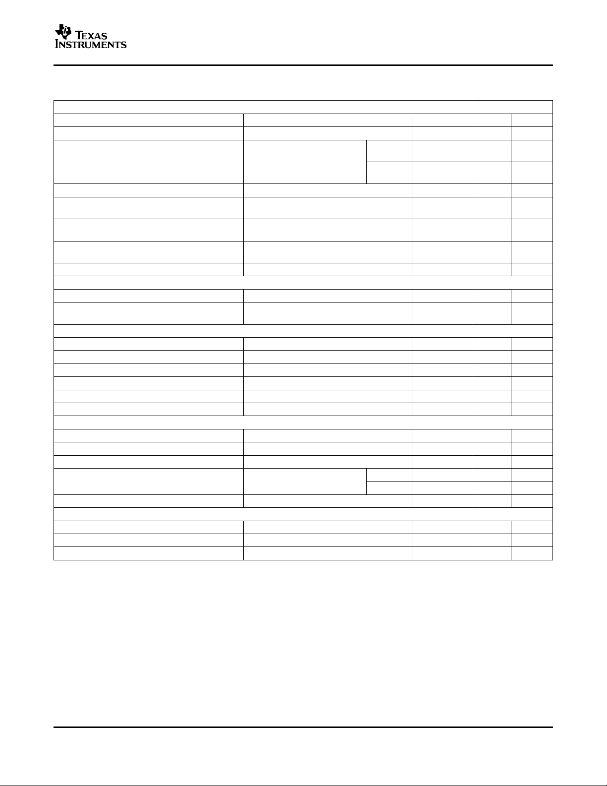
D, JG PACKAGE
(TOP VIEW)
192013 2
17
18
16
15
14
1312119 10
5
4
6
7
8
NC
OUTB
NC
REF
NC
NC
SCLK
NC
CS
NC
NC
DIN
NC
NC
OUTA
NC
AGND
NC
NC
FK PACKAGE
(TOP VIEW)
DD
V
SLAS225C – JUNE 1999 – REVISED JANUARY 2004
2.7-V TO 5.5-V LOW-POWER DUAL 12-BIT DIGITAL-TO-ANALOG CONVERTER WITH
INTERNAL REFERENCE AND POWER DOWN
FEATURES
• Dual 12-Bit Voltage Output DAC
• Programmable Internal Reference
• Programmable Settling Time:
– 1 µs in Fast Mode,
– 3.5 µs in Slow Mode
• Compatible With TMS320 and SPI™ Serial
Ports
• Differential Nonlinearity <0.5 LSB Typ
• Monotonic Over Temperature
APPLICATIONS
• Digital Servo Control Loops
• Digital Offset and Gain Adjustment
• Industrial Process Control
• Machine and Motion Control Devices
• Mass Storage Devices
TLV5638
DESCRIPTION
The TLV5638 is a dual 12-bit voltage output DAC with a flexible 3-wire serial interface. The serial interface allows
glueless interface to TMS320, SPI™, QSPI™, and Microwire™ serial ports. It is programmed with a 16-bit serial
string containing 4 control and 12 data bits.
The resistor string output voltage is buffered by a x2 gain rail-to-rail output buffer. The buffer features a Class AB
output stage to improve stability and reduce settling time. The programmable settling time of the DAC allows the
designer to optimize speed vs power dissipation. With its on-chip programmable precision voltage reference, the
TLV5638 simplifies overall system design.
Because of its ability to source up to 1 mA, the reference can also be used as a system reference. Implemented
with a CMOS process, the device is designed for single supply operation from 2.7 V to 5.5 V. It is available in an
8-pin SOIC package to reduce board space in standard commercial, industrial, and automotive temperature
ranges. It is also available in JG and FK packages in the military temperature range.
SPI, QSPI are trademarks of Motorola, Inc.
Microwire is a trademark of National Semiconductor Corporation.
PRODUCTION DATA information is current as of publication date.
Products conform to specifications per the terms of the Texas
Instruments standard warranty. Production processing does not
necessarily include testing of all parameters.
Copyright © 1999–2004, Texas Instruments Incorporated
Please be aware that an important notice concerning availability, standard warranty, and use in critical applications of Texas
Instruments semiconductor products and disclaimers thereto appears at the end of this data sheet.
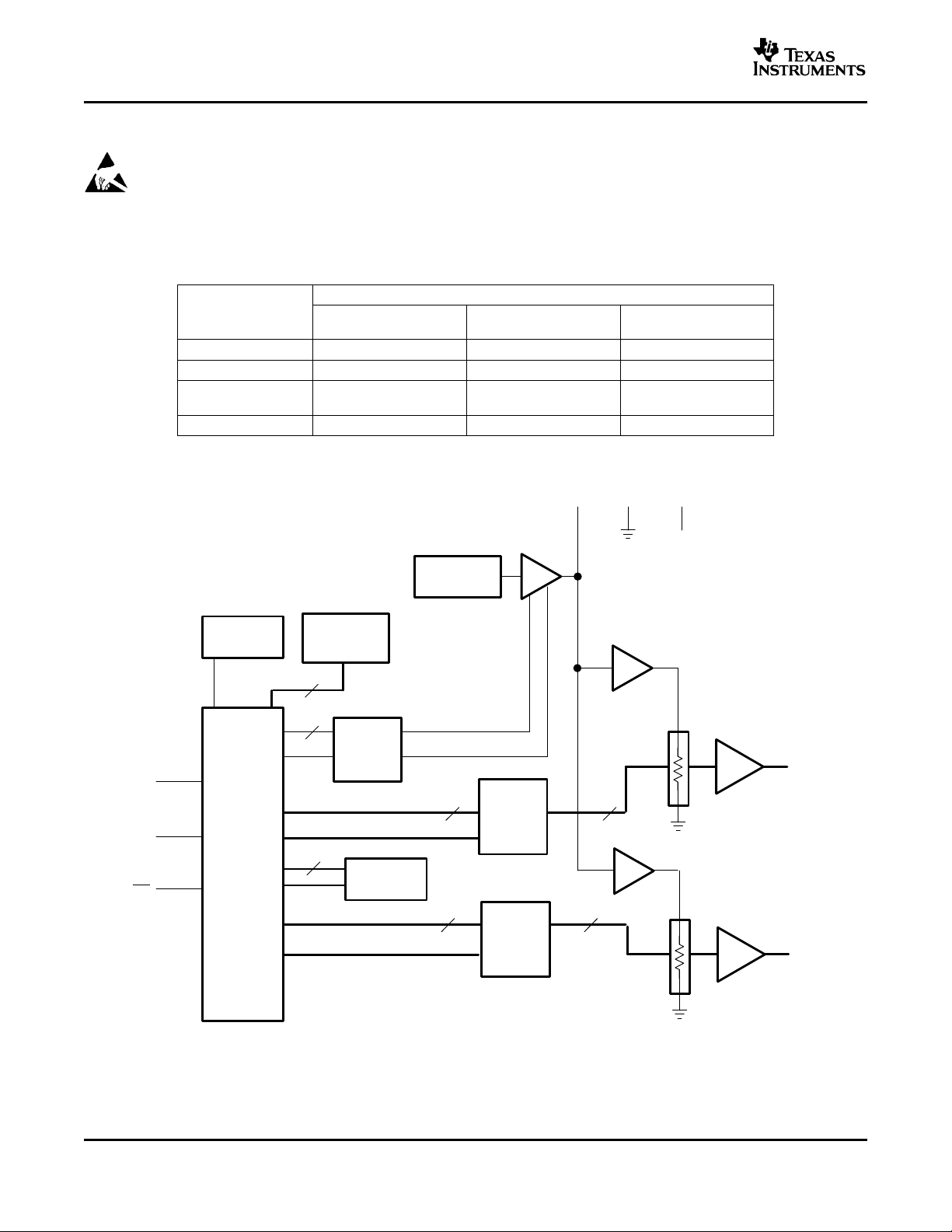
www.ti.com
Serial
Interface
and
Control
12-Bit
DAC B
Latch
SCLK
DIN
CS
OUTA
Power-On
Reset
x2
12
2-Bit
Control
Latch
Power
and Speed
Control
2
Voltage
Bandgap
PGA With
Output Enable
12-Bit
DAC A
Latch
12
REF AGND V
DD
2
12 12
OUTB
x2
Buffer
12
TLV5638
SLAS225C – JUNE 1999 – REVISED JANUARY 2004
This integrated circuit can be damaged by ESD. Texas Instruments recommends that all integrated
circuits be handled with appropriate precautions. Failure to observe proper handling and installation
procedures can cause damage.
ESD damage can range from subtle performance degradation to complete device failure. Precision
integrated circuits may be more susceptible to damage because very small parametric changes could
cause the device not to meet its published specifications.
T
A
0 ° C to 70 ° C TLV5638CD — —
40 ° C to 85 ° C TLV5638ID — —
40 ° C to 125 ° C — —
55 ° C to 125 ° C — TLV5638MJG TLV5638MFK
AVAILABLE OPTIONS
PACKAGE
SOIC CERAMIC DIP 20 PAD LCCC
(D) (JG) (FK)
TLV5638QD
TLV5638QDR
FUNCTIONAL BLOCK DIAGRAM
2
www.ti.com
SLAS225C – JUNE 1999 – REVISED JANUARY 2004
Terminal Functions
TERMINAL
NAME NO.
AGND 5 P Ground
CS 3 I Chip select. Digital input active low, used to enable/disable inputs
DIN 1 I Digital serial data input
OUT A 4 O DAC A analog voltage output
OUT B 7 O DAC B analog voltage output
REF 6 I/O Analog reference voltage input/output
SCLK 2 I Digital serial clock input
V
DD
I/O/P DESCRIPTION
8 P Positive power supply
ABSOLUTE MAXIMUM RATINGS
over operating free-air temperature range (unless otherwise noted)
Supply voltage (V
Reference input voltage range -0.3 V to V
Digital input voltage range -0.3 V to V
Operating free-air temperature range, T
Storage temperature range, T
Lead temperature 1,6 mm (1/16 inch) from case for 10 seconds 260 ° C
(1) Stresses beyond those listedunder, , absolute maximum ratings” may cause permanent damage to thedevice. These are stress ratings
only, and functional operation of the deviceat these or any other conditions beyond those indicated under, , recommended operating
conditions” is not implied. Exposure toabsolute-maximum-rated conditions for extended periods may affect devicereliability.
to AGND) 7 V
DD
A
TLV5638C 0 ° C to 70 ° C
TLV5638I -40 ° C to 85 ° C
TLV5638Q -40 ° C to 125 ° C
TLV5638M -55 ° C to 125 ° C
stg
(1)
UNIT
+ 0.3 V
DD
+ 0.3 V
DD
-65 ° C to 150 ° C
TLV5638
DISSIPATION RATING TABLE
PACKAGE
D 635 mW 5.08 mW/ ° C 407 mW 330 mW 127 mW
FK 1375 mW 11.00 mW/ ° C 880 mW 715 mW 275 mW
JG 1050 mW 8.40 mW/ ° C 672 mW 546 mW 210 mW
(1) This is the inverse of thetraditional Junction-to-Ambient thermal Resistance (R θJA). Thermal Resistances are not production testedand
are for informational purposes only.
TA≤ 25 ° C DERATING FACTOR TA= 70 ° C TA= 85 ° C TA= 125 ° C
POWER RATING ABOVE TA= 25 ° C
(1)
POWER RATING POWER RATING POWER RATING
3
www.ti.com
TLV5638
SLAS225C – JUNE 1999 – REVISED JANUARY 2004
RECOMMENDED OPERATING CONDITIONS
V
= 5 V 4.5 5 5.5 V
Supply voltage, V
DD
Power on reset, POR 0.55
High-level digital input voltage, V
Low-level digital input voltage, V
Reference voltage, V
Reference voltage, V
Load resistance, R
Load capacitance, C
Clock frequency, f
to REF terminal V
ref
to REF terminal V
ref
L
L
CLK
Operating free-air temperature, T
IH
IL
A
(1) This parameter is not testedfor Q and M suffix devices.
(2) Due to the x2 output buffer,a reference input voltage ≥ (V
internal reference must be disabled, if an externalreference is used.
DD
V
= 3 V 2.7 3 3.3 V
DD
V
= 2.7 V 2 V
DD
V
= 5.5 V 2.4
DD
V
= 2.7 V 0.6 V
DD
V
= 5.5 V V
DD
= 5 V
DD
= 3 V
DD
TLV5638C and TLV5638I 1
TLV5638Q and TLV5638M 0.8
(2)
(2)
TLV5638C 0 70
TLV5638I 40 85
TLV5638Q 40 125
TLV5638M 55 125
-0.4 V)/2 causes clipping of the transfer function.The output buffer of the
DD
MIN NOM MAX UNIT
(1)
(1)
2
AGND 2.048 VDD-1.5 V
AGND 1.024 VDD-1.5 V
2 k Ω
100 pF
20 MHz
V
° C
ELECTRICAL CHARACTERISTICS
over recommended operating conditions, V
POWER SUPPLY
PARAMETER TEST CONDITIONS UNIT
I
PSRR Power supply rejection ratio dB
(1) Power supply rejection ratioat zero scale is measured by varying VDDand is given by: PSRR = 20 log [(E
(2) Power supply rejection ratioat full scale is measured by varying VDDand is given by: PSRR = 20 log [(E
Power supply current All inputs = AGND or VDD,
DD
Power-down supply current 0.01 10 µA
-E
(V
min))/V
ZS
DD
-E
min))/V
G(VDD
max]
DD
max]
DD
ref
No load,
DAC latch = 0x800
Zero scale,
Full scale,
= 2.048 V, V
(1)
(2)
= 1.024 V (unless otherwise noted)
ref
VDD= 5 V,
Int. ref.
V
= 3 V,
DD
Int. ref.
V
= 5 V,
DD
Ext. ref.
V
= 3 V,
DD
Ext. ref.
TLV5638C, I
TLV5638M
MIN TYP MAX
Fast 4.3 7
Slow 2.2 3.6
Fast 3.8 6.3
Slow 1.8 3.0
Fast 3.9 6.3
Slow 1.8 3.0
Fast 3.5 5.7
Slow 1.5 2.6
65
65
(V
max)
ZS
DD
max)
G(VDD
mA
mA
mA
mA
4
www.ti.com
TLV5638
SLAS225C – JUNE 1999 – REVISED JANUARY 2004
ELECTRICAL CHARACTERISTICS (CONTINUED)
over recommended operating conditions, V
STATIC DAC SPECIFICATIONS
PARAMETER TEST CONDITIONS MIN TYP MAX UNIT
Resolution 12 bits
INL See
DNL Differential nonlinearity See
E
ZS
EZSTC See
E
G
EGT
C
OUTPUT SPECIFICATIONS
V
O
REFERENCE PIN CONFIGURED AS OUTPUT (REF)
Vref(OUTL) Low reference voltage 1.003 1.024 1.045 V
Vref(OUTH) High reference voltage V
Iref(source) Output source current 1 mA
Iref(sink) Output sink current -1 mA
PSRR Power supply rejection ratio -65 dB
REFERENCE PIN CONFIGURED AS INPUT (REF)
V
I
R
I
C
I
DIGITAL INPUTS
I
IH
I
IL
C
i
(1) The relative accuracy orintegral nonlinearity (INL) sometimes referred to as linearity error, is themaximum deviation of the output from
the line between zero and full scaleexcluding the effects of zero code and full-scale errors. Tested from code 32to 4095.
(2) The differential nonlinearity(DNL) sometimes referred to as differential error, is the difference betweenthe measured and ideal 1 LSB
amplitude change of any two adjacent codes.Monotonic means the output voltage changes in the same direction (or remainsconstant)
as a change in the digital input code.
(3) Zero-scale error is thedeviation from zero voltage output when the digital input code iszero.
(4) Zero-scale-error temperaturecoefficient is given by: E
(5) Gain error is the deviationfrom the ideal output (2V
(6) Gain temperature coefficientis given by: EGTC = [EG(T
(7) Reference feedthrough ismeasured at the DAC output with an input code = 0x000.
Integral nonlinearity, end point adjusted
Zero-scale error (offset error at zero
scale)
Zero-scale-error temperature coefficient
Gain error See
Gain error temperature coefficient See
Output voltage RL= 10 k Ω 0 VDD-0.4 V
Output load regulation accuracy VO= 4.096 V, 2.048 V, RL= 2 k Ω ± 0.25
Load capacitance 100 pF
Input voltage 0 VDD-1.5 V
Input resistance 10 M Ω
Input capacitance 5 pF
Reference input bandwidth REF = 0.2 Vpp+ 1.024 V dc
Reference feedthrough REF = 1 Vppat 1.024 V dc
HIgh-level digital input current VI= V
Low-level digital input current VI= 0 V -1 µA
Input capacitance 8 pF
= 2.048 V, V
ref
= 1.024 V (unless otherwise noted)
ref
C and I
(1)
suffixes
Q and M
suffixes
(2)
(3)
See
(4)
(5)
(6)
> 4.75 V 2.027 2.048 2.069 V
DD
± 1.7 ± 4 LSB
± 1.7 ± 6 LSB
± 0.4 ± 1 LSB
10 ppm/ ° C
10 ppm/ ° C
Fast 1.3 MHz
Slow 525 kHz
(7)
DD
TC =[E
ZS
- 1 LSB) withan output load of 10 k Ω excluding the effects of thezero-error.
ref
max
(T
) - EZS(T
ZS
max
) -E
)]/V
G(Tmin
× 10
ref
)]/V
min
6
/(T
max
6
× 10
/(T
ref
- T
).
min
-T
max
).
min
-80 dB
± 24 mV
± 0.6
1 µA
% full
scale V
% full
scale V
5
www.ti.com
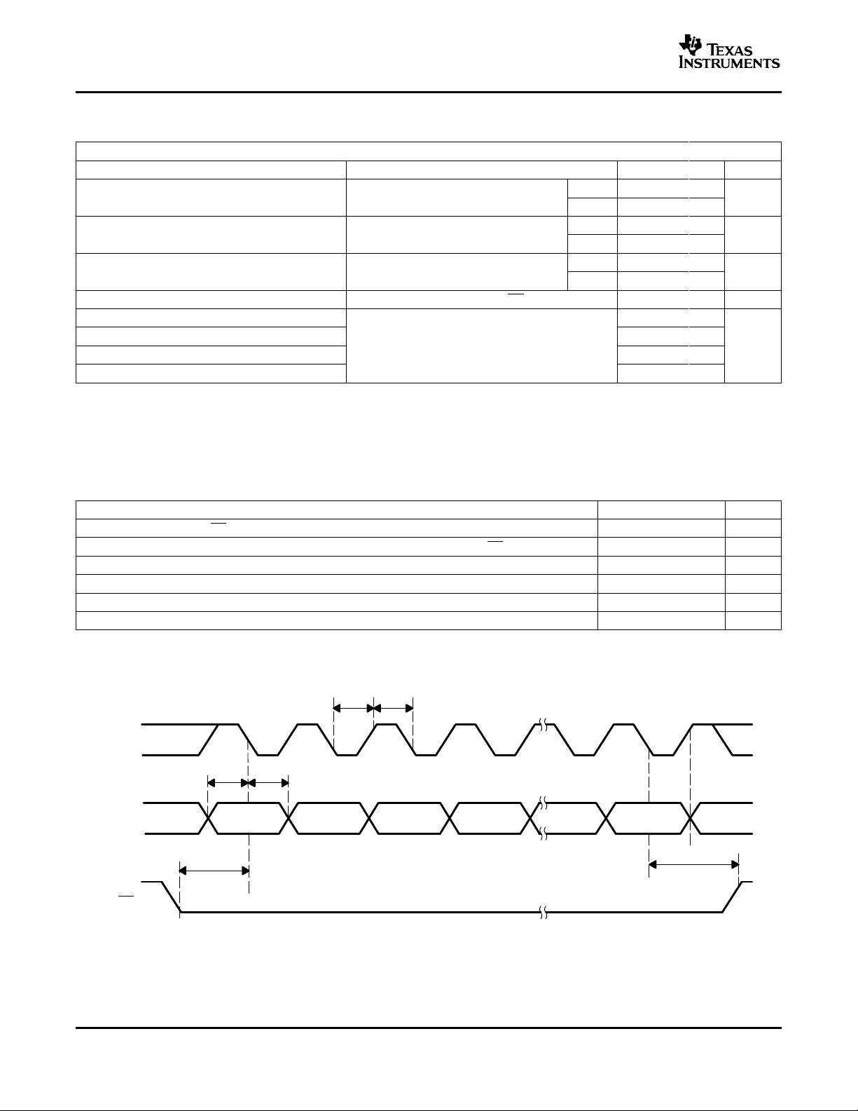
t
wL
SCLK
CS
DIN
D15 D14 D13 D12 D1 D0 XX
1
X
2 3 4 5 15 16
X
t
wH
t
su(D)th(D)
t
su(CS-CK)
t
su(C16-CS)
TLV5638
SLAS225C – JUNE 1999 – REVISED JANUARY 2004
ELECTRICAL CHARACTERISTICS (CONTINUED)
over recommended operating conditions, V
ANALOG OUTPUT DYNAMIC PERFORMANCE
PARAMETER TEST CONDITIONS MIN TYP MAX UNIT
t
s(FS)
t
s(CC)
SR Slew rate RL= 10 k Ω , CL= 100 pF, See
SNR Signal-to-noise ratio 69 74
S/(N+D) Signal-to-noise + distortion 58 67
THD Total harmonic distortion 69 57
(1) Settling time is the timefor the output signal to remain within ± 0.5 LSB of the final measured value fora digital input code change of
(2) Settling time is the timefor the output signal to remain within ± 0.5 LSB of the final measured valuefor a digital input code change of one
(3) Slew rate determines thetime it takes for a change of the DAC output from 10% to 90% full-scalevoltage.
Output settling time, full scale RL= 10 k Ω , CL= 100 pF, See
Output settling time, code to code RL= 10 k Ω , CL= 100 pF, See
Glitch energy DIN = 0 to 1, FCLK = 100 kHz, CS = V
Spurious free dynamic range 57 72
0x020 to 0xFDF and 0xFDF to 0x020 respectively.Not tested, assured by design.
count. Not tested, assured bydesign.
= 2.048 V, V
ref
= 1.024 V (unless otherwise noted)
ref
fs= 480 kSPS, f
CL= 100 pF
(1)
= 1 kHz, RL= 10 k Ω ,
out
Fast 1 3
Slow 3.5 7
(2)
Fast 0.5 1.5
Slow 1 2
(3)
Fast 12
Slow 1.8
DD
5 nV-s
µs
µs
V/µs
dB
DIGITAL INPUT TIMING REQUIREMENTS
t
su(CS-CK)
t
su(C16-CS)
t
wH
t
wL
t
su(D)
t
h(D)
MIN NOM MAX UNIT
Setup time, CS low before first negative SCLK edge 10 ns
Setup time, 16
th
negative SCLK edge (when D0 is sampled) before CS rising edge 10 ns
SCLK pulse width high 25 ns
SCLK pulse width low 25 ns
Setup time, data ready before SCLK falling edge 10 ns
Hold time, data held valid after SCLK falling edge 5 ns
PARAMETER MEASURMENT INFORMATION
6
Figure 1. Timing Diagram
 Loading...