

TLV5621I
LOW-POWER QUADRUPLE 8-BIT DIGITAL-TO-ANALOG CONVERTER
SLAS138B – APRIL 1996 – REVISED FEBRUARY 1997
1
POST OFFICE BOX 655303 • DALLAS, TEXAS 75265
D
2.7-V to 5.5-V Single-Supply Operation
D
Four 8-Bit Voltage Output DACs
D
One-Half Power 8-Bit Voltage Output DAC
D
Fast Serial Interface...1 MHz Max
D
Simple Two-Wire Interface In Single
Buffered Mode
D
High-Impedance Reference Inputs For Each
DAC
D
Programmable for 1 or 2 Times Output
Range
D
Simultaneous-Update Facility In
Double-Buffered Mode
D
Internal Power-On Reset
D
Industry Temperature Range
D
Low Power Consumption
D
Half-Buffered Output
D
Power-Down Mode
applications
D
Programmable V oltage Sources
D
Digitally-Controlled Amplifiers/Attenuators
D
Cordless/Wireless Communications
D
Automatic Test Equipment
D
Portable Test Equipment
D
Process Monitoring and Control
D
Signal Synthesis
description
The TL V5621I is a quadruple 8-bit voltage output
digital-to-analog converter (DAC) with buffered
reference inputs (high impedance). The DAC
produces an output voltage that ranges between
either one or two times the reference voltages and
GND, and the DAC is monotonic. The device is
simple to use since it operates from a single
supply of 2.7 V to 5.5 V . A power-on reset function
is incorporated to provide repeatable start-up
conditions. A global hardware shut-down terminal
and the capability to shut down each individual
DAC with software are provided to minimize
power consumption.
Digital control of the TL V5621I is over a simple 3-wire serial bus that is CMOS compatible and easily interfaced
to all popular microprocessor and microcontroller devices. A TLV5621I 11-bit command word consists of
eight bits of data, two DAC select bits, and a range bit for selection between the times one or times two output
range. The TLV5621I digital inputs feature Schmitt triggers for high noise immunity. The DAC registers are
double buffered which allows a complete set of new values to be written to the device, and then under control
of the HWACT signal, all of the DAC outputs are updated simultaneously.
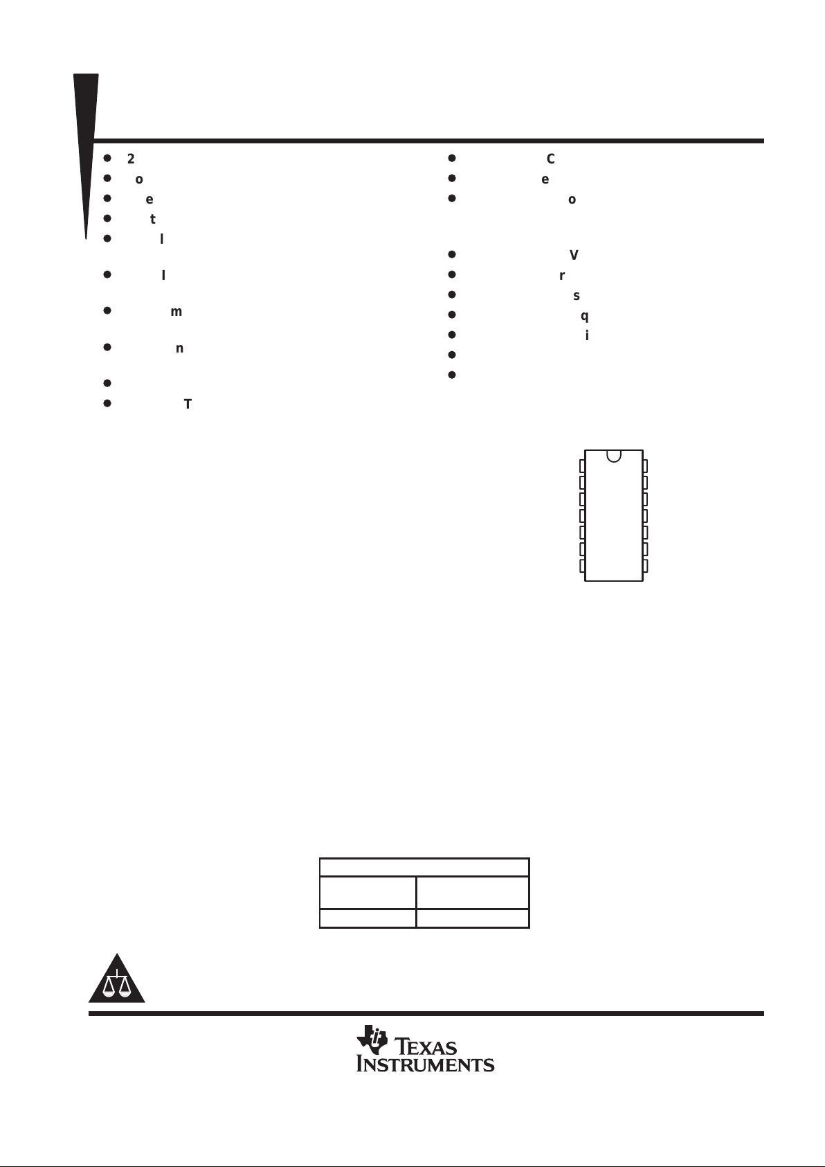
The 14-terminal small-outline (D) package allows digital control of analog functions in space-critical
applications. The TLV5621I does not require external trimming. The TLV5621I is characterized for operation
from –40°C to 85°C.
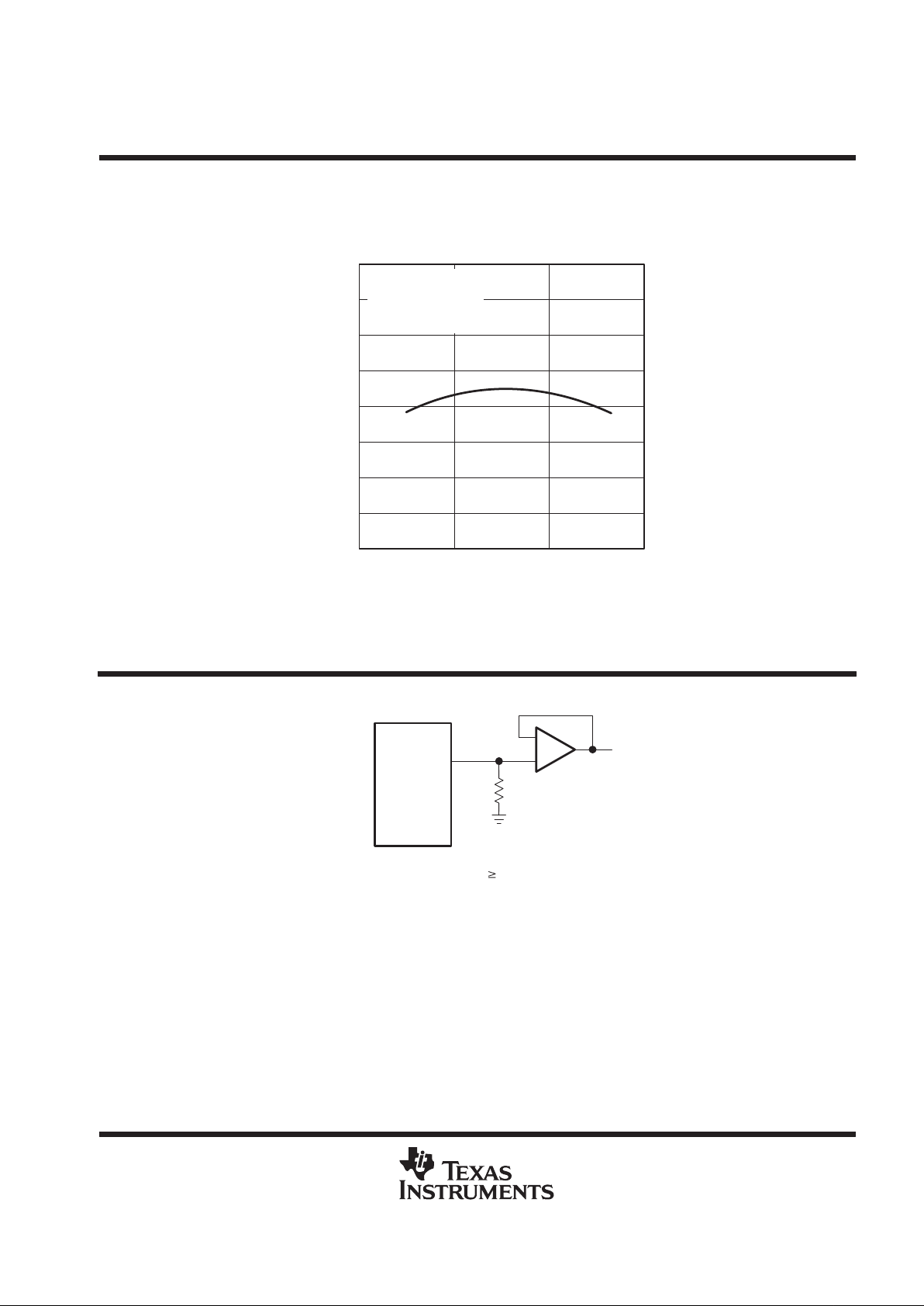
AVAILABLE OPTIONS
PACKAGE
T
A
SMALL OUTLINE
(D)
–40°C to 85°C TLV5621ID
Please be aware that an important notice concerning availability, standard warranty, and use in critical applications of
Texas Instruments semiconductor products and disclaimers thereto appears at the end of this data sheet.
GND
REFA
REFB
REFC
REFD
DATA
CLK
1
2
3
4
5
6
7
14
13
12
11
10
9
8
V
DD
HWACT
DACA
DACB
DACC
DACD
EN
D PACKAGE
(TOP VIEW)
PRODUCTION DATA information is current as of publication date.
Products conform to specifications per the terms of Texas Instruments
standard warranty. Production processing does not necessarily include
testing of all parameters.
Copyright 1997, Texas Instruments Incorporated
TLV5621I
LOW-POWER QUADRUPLE 8-BIT DIGITAL-TO-ANALOG CONVERTER
SLAS138B – APRIL 1996 – REVISED FEBRUARY 1997
2
POST OFFICE BOX 655303 • DALLAS, TEXAS 75265
functional block diagram
Power-On
Reset
Serial
Interface
× 2
DAC
LatchLatch
Latch Latch
DAC
× 2
× 2
DAC
LatchLatch
Latch Latch
DAC
× 2
REFA
+
–
+
–
+
–
+
–
+
–
+
–
+
–
+
–
REFB
REFC
CLK
REFD
DATA
EN
DACA
DACB
DACC
DACD
8 8
8
8
8
8
8
8
HWACT
Terminal Functions
TERMINAL
NAME NO.
I/O
DESCRIPTION
CLK 7 I Serial interface clock, data enters on the negative edge
DACA 12 O DAC A analog output
DACB 11 O DAC B analog output
DACC 10 O DAC C analog output
DACD 9 O DAC D analog output
DATA 6 I Serial-interface digital-data input
EN 8 I Input enable
GND 1 Ground return and reference
HWACT 13 I Global hardware activate
REFA 2 I Reference voltage input to DACA
REFB 3 I Reference voltage input to DACB
REFC 4 I Reference voltage input to DACC
REFD 5 I Reference voltage input to DACD
V
DD
14 Positive supply voltage
detailed description
The TLV5621 is implemented using four resistor-string DACs. The core of each DAC is a single resistor with
256 taps, corresponding to the 256 possible codes listed in T able 1. One end of each resistor string is connected
to GND and the other end is fed from the output of the reference input buffer . Monotonicity is maintained by use
of the resistor strings. Linearity depends upon the matching of the resistor elements and upon the performance
of the output buffer . Because the inputs are buf fered, the DACs always present a high-impedance load to the
reference source.
TLV5621I
LOW-POWER QUADRUPLE 8-BIT DIGITAL-TO-ANALOG CONVERTER
SLAS138B – APRIL 1996 – REVISED FEBRUARY 1997
3
POST OFFICE BOX 655303 • DALLAS, TEXAS 75265
Each DAC output is buffered by a configurable-gain output amplifier, which can be programmed to times one
or times two gain.
On power-up, the DACs are reset to CODE 0.
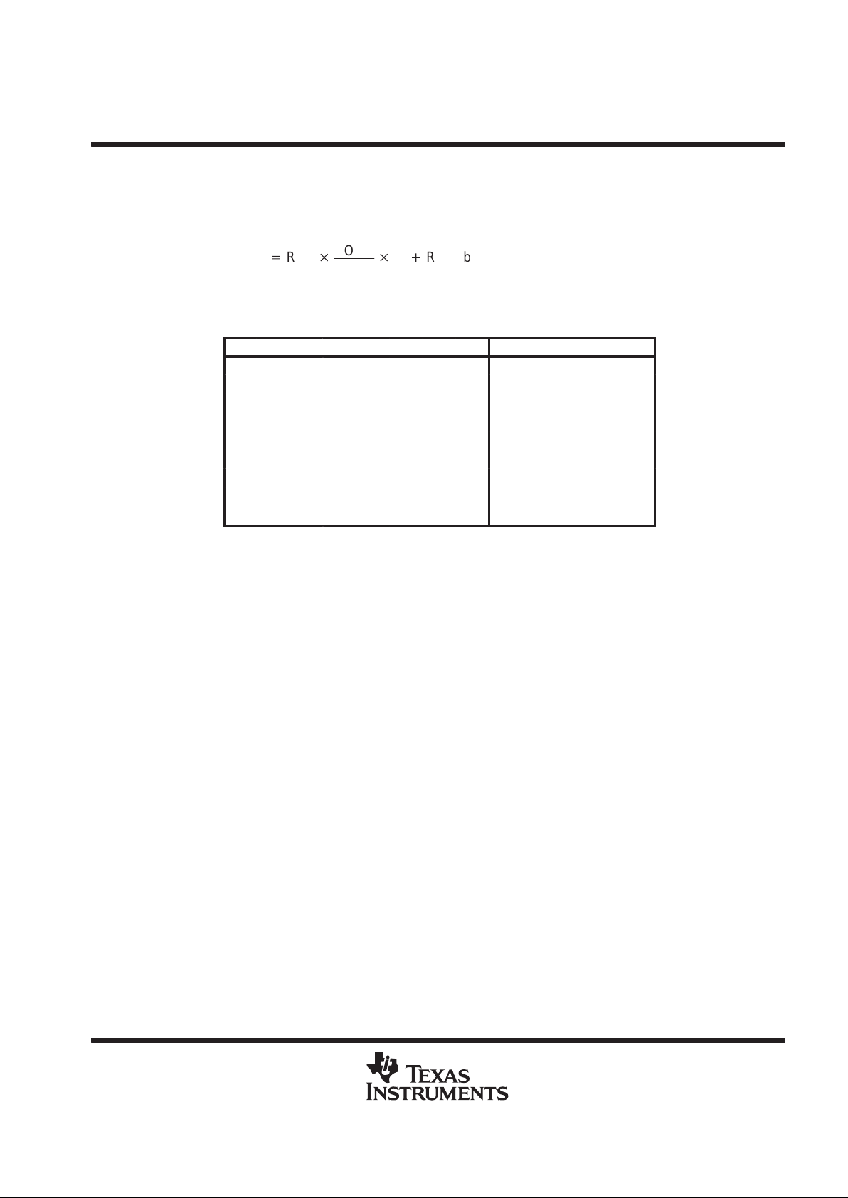
Each output voltage is given by:
VO(DACA|B|C|D)+REF
CODE
256
(1)
RNG bit value)
where CODE is in the range 0 to 255 and the range (RNG) bit is a 0 or 1 within the serial control word.
Table 1. Ideal-Output Transfer
D7 D6 D5 D4 D3 D2 D1 D0 OUTPUT VOLTAGE
0 0 0 0 0 0 0 0 GND
0 0000001 (1/256) × REF (1+RNG)
• ••••••• •
•••••••• •
01111111 (127/256) × REF (1+RNG)
1 0000000 (128/256) × REF (1+RNG)
• ••••••• •
•••••••• •
11111111 (255/256) × REF (1+RNG)
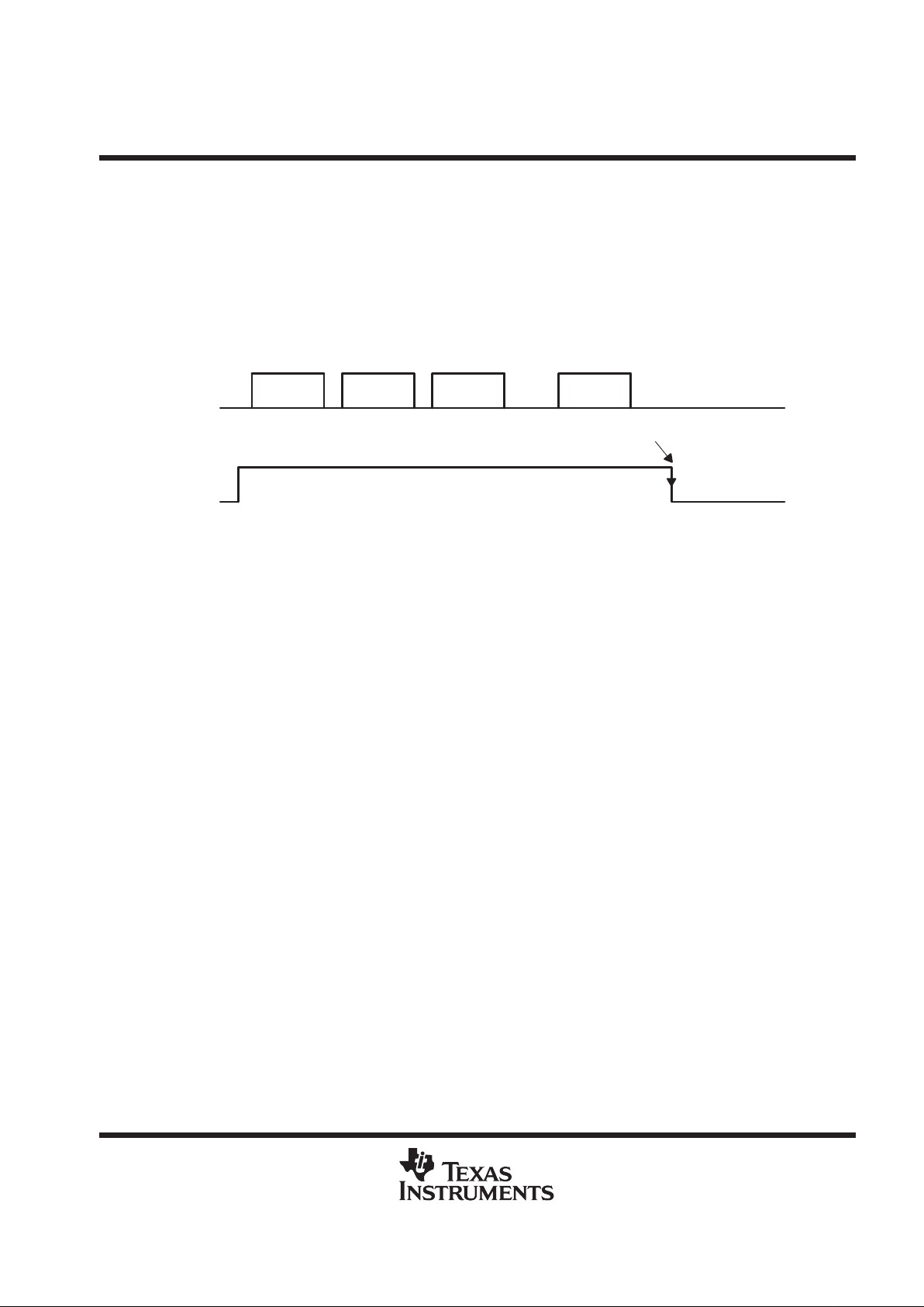
data interface
The data interface has two modes of operation; single and double buffered. Both modes serially clock in bits
of data using DA T A and CLK whenever EN is high. When EN is low, CLK is disabled and data cannot be loaded
into the buffers.
In the single buffered mode, the DAC outputs are updated on the last/twelfth falling edge of CLK, so this mode
only requires a two-wire interface with EN tied high (see Figure 1 and Figure 2).
In the double buffered mode (startup default), the outputs of the DACs are updated on the falling edge of the
EN strobe (see Figure 3 and Figure 4). This allows multiple devices to share data and clock lines by having only
separate EN lines.
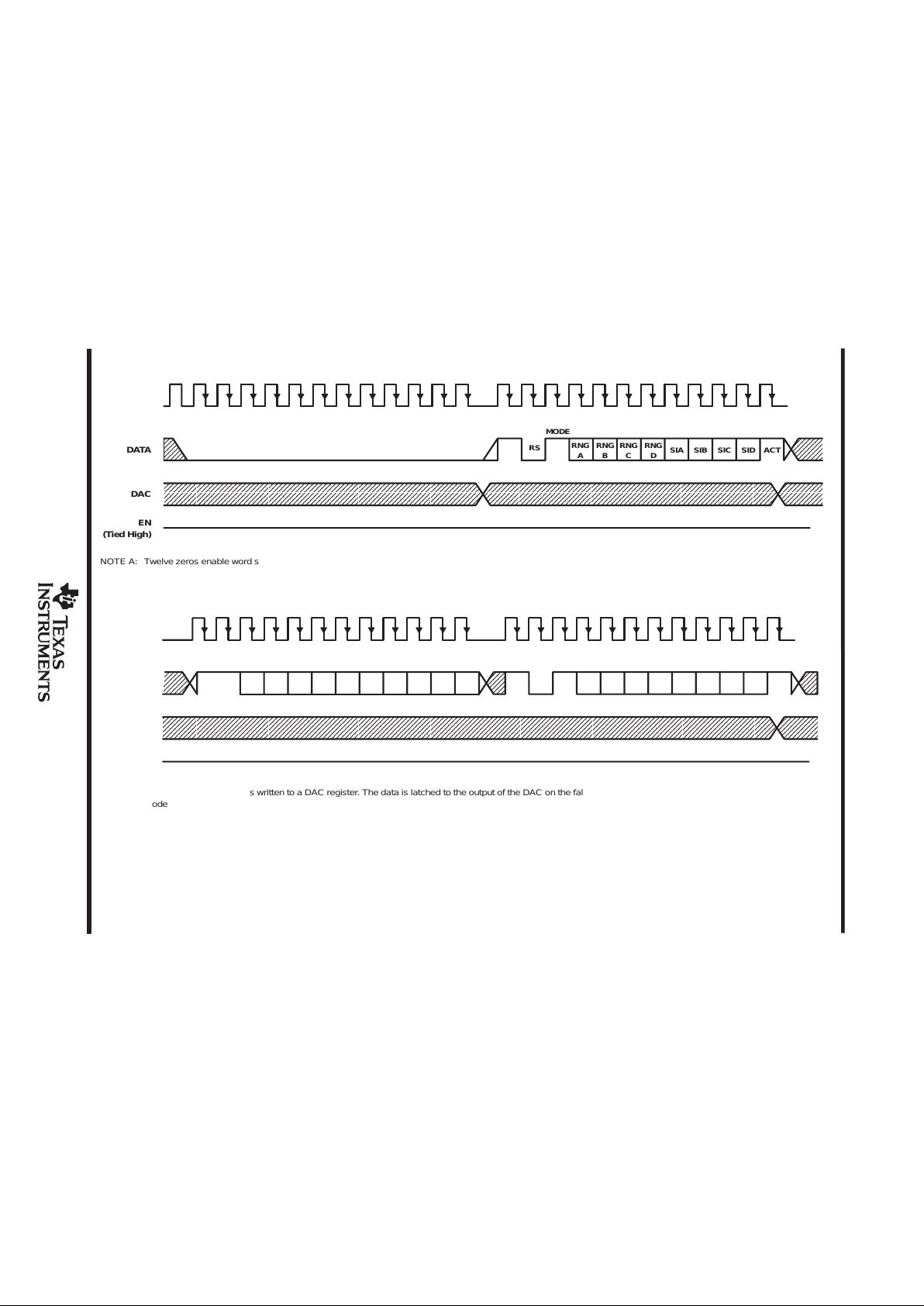
single-buffer mode (MODE = 1)
When a two wire interface is used, EN is tied high and the input to the device is always active; therefore, random
data can be clocked into the input latch. In order to regain word synchronization, twelve zeros are clocked in
as shown in Figure 1, and then a data or control word is clocked in. In Figure 1, the MODE bit is set to one, and
a control word is clocked in with the DAC outputs becoming active after the last falling edge of the control word.
Figure 2 shows valid data being written to a DAC, note that CLK is held low while the data is invalid. Data can
be written to all four DACs and then the control word is clocked in which sets the MODE bit to 1. At the end of
the control word, the data is latched to the inputs of the DACs.
Note that once the MODE bit has been set, it is not possible to clear it, i.e., it is not possible to move from single
to double-buffered mode.
SLAS138B – APRIL 1996 – REVISED FEBRUAR Y 1997
TLV5621I
LOW-POWER QUADRUPLE 8-BIT DIGITAL-TO-ANALOG CONVERTER
Template Release Date: 7–11–94
4
POST OFFICE BOX 655303 DALLAS, TEXAS 75265
•
CLK
RS
MODE
RNGARNGBRNGCRNG
D
SIA SIB SIC SID ACT
DATA
DAC
EN
(Tied High)
NOTE A: Twelve zeros enable word synchronization and the output can change after the leading edge of CLK depending on the data in the latches.
Figure 1. Register Write Operation Following Noise or Undefined Levels on DATA or CLK (Single-Buffer Mode)
CLK
RS
MODE
RNGARNGBRNGCRNG
D
SIA SIB SIC SID ACTDATA
DAC
EN
(Tied High)
NOTE A: EN is held high and data is written to a DAC register. The data is latched to the output of the DAC on the falling edge of the last CLK of the control word, where the
mode is set.
RS A1 A0 D7 D6 D5 D4 D3 D2 D1 D0
Figure 2. First Nonzero Write Operation After Startup (EN = High)
TLV5621I
LOW-POWER QUADRUPLE 8-BIT DIGITAL-TO-ANALOG CONVERTER
SLAS138B – APRIL 1996 – REVISED FEBRUARY 1997
5
POST OFFICE BOX 655303 • DALLAS, TEXAS 75265
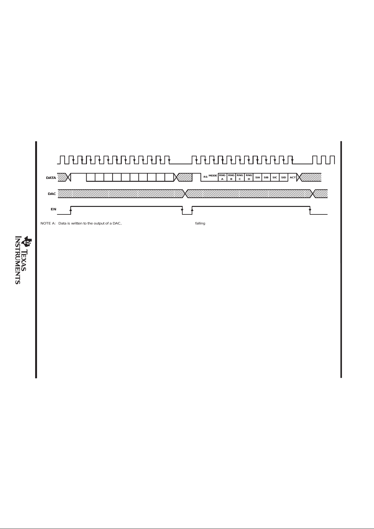
double-buffered mode (MODE = 0)
In this mode, data is only latched to the output of the DACs on the falling edge of the EN strobe. Therefore, all
four DACs can be written to before updating their outputs.
Any number of input data blocks can be written with all having the same length. Subsequent data blocks simply
overwrite previous ones with the same address until EN goes low.
Multiple data blocks can be written in any sequence provided signal timing limits are met. The negative going
edge of EN terminates and latches all data.
Data Latched Into DAC Control Registers and Control Word
Multiple Random Sequence Data Blocks
DATA
EN
Figure 3. Data and Control Serial Control
SLAS138B – APRIL 1996 – REVISED FEBRUAR Y 1997
TLV5621I
LOW-POWER QUADRUPLE 8-BIT DIGITAL-TO-ANALOG CONVERTER
Template Release Date: 7–11–94
6
POST OFFICE BOX 655303 DALLAS, TEXAS 75265
•
CLK
ПППППППППППППППППП
RS
MODE
RNGARNGBRNGCRNG
D
SIA SIB SIC SID ACT
DATA
DAC
EN
NOTE A: Data is written to the output of a DAC, and the data is latched to the output on the falling edge of EN. A control word then selects double-buffered mode. When the
range is changed, the output changes on the falling edge of EN.
RS A1 A0 D7 D6 D5 D4 D3 D2 D1 D0
Figure 4. First Nonzero Write Operation After Startup

TLV5621I
LOW-POWER QUADRUPLE 8-BIT DIGITAL-TO-ANALOG CONVERTER
SLAS138B – APRIL 1996 – REVISED FEBRUARY 1997
7
POST OFFICE BOX 655303 • DALLAS, TEXAS 75265
control register
The control register contains ten active bits. Four bits are range select bits as on the TLC5620. The register also
contains a software shutdown bit (ACT) and four shutdown inhibit bits (SIA, SIB, SIC, SID). The shutdown inhibit
bits act on each DAC (DACA through DACD). The mode select bit is used to change between single and double
buffered modes. The bits in the control register are listed in Table 2.
Table 2. Control Register Bits
BIT FUNCTION
MODE Selection bit for type of interface (see data interface section)
RNG A Range select bit for DACA, 0 = 1, 1 = 2
RNG B Range select bit for DACB, 0 = 1, 1 = 2
RNG C Range select bit for DACC, 0 = 1, 1 = 2
RNG D Range select bit for DACD, 0 = 1, 1 = 2
SIA Shutdown inhibit bit for DACA
SIB Shutdown inhibit bit for DACB
SIC Shutdown inhibit bit for DACC
SID Shutdown inhibit bit for DACD
ACT Software shutdown bit
The SIx bits inhibit the actions of the shutdown bits as shown in Table 3. When the ACT bit is 1 or the HW ACT
signal is high (active), the inhibit bits act as enable bits in inverse logic terms. The ACT software shutdown bit
and HWACT (asynchronously acting hardware terminal) are logically ORed together.
This configuration allows any combination of DACs to be shut down to save power.
Table 3. Shutdown Inhibit Bits and HWACT Signal
SIx ACT HWACT DACx STATUS
0 0 L Shutdown (see Note 1)
0 0 H Shutdown
0 1 L Shutdown
0 1 H Active (see Note 1)
1 0 L Active
1 0 H Active
1 1 L Active
1 1 H Active
NOTE 1: Sense of HWACT terminal and ACT bit were changed from early
versions of this specification.
The values of the input address select bits, A0 and A1, and the updated DAC are listed in Table 4.
Table 4. Serial Input Decode
INPUT ADDRESS SELECT BITS
A1 A0
DAC UPDATED
0 0 DACA
0 1 DACB
1 0 DACC
1 1 DACD

TLV5621I
LOW-POWER QUADRUPLE 8-BIT DIGITAL-TO-ANALOG CONVERTER
SLAS138B – APRIL 1996 – REVISED FEBRUARY 1997
8
POST OFFICE BOX 655303 • DALLAS, TEXAS 75265
power-on reset
Power-on reset circuitry is available on the TL V5621I. The threshold to trigger a power-on reset is 1.95 V typical
(1.4 V min and 2.5 V max). For a power-on reset, all DACs are shut down. The control register bit values and
states after a power-on reset are listed in Table 5.
Table 5. Control Register Bit Values and States After Power-On Reset
BIT VALUE STATE AFTER POWER-ON RESET
MODE 0 Double buffer mode selected
RNG A 1 Range 2
RNG B 1 Range 2
RNG C 1 Range 2
RNG D 1 Range 2
SIA 0 Shutdown affects DACA according to ACT state
SIB 0 Shutdown affects DACB according to ACT state
SIC 0 Shutdown affects DACC according to ACT state
SID 0 Shutdown affects DACD according to ACT state
ACT 0 DACs in shutdown state

TLV5621I
LOW-POWER QUADRUPLE 8-BIT DIGITAL-TO-ANALOG CONVERTER
SLAS138B – APRIL 1996 – REVISED FEBRUARY 1997
9
POST OFFICE BOX 655303 • DALLAS, TEXAS 75265
linearity, offset, and gain error using single-end supplies
When an amplifier is operated from a single supply , the voltage offset can still be either positive or negative. With
a positive offset, the output voltage changes on the first code change. With a negative offset the output voltage
may not change with the first code depending on the magnitude of the offset voltage.
The output amplifier attempts to drive the output to a negative voltage. However, because the most negative
supply rail is ground, the output cannot drive below ground and clamps the output at 0 V.
The output voltage then remains at zero until the input code value produces a sufficient positive output voltage
to overcome the negative offset voltage, resulting in the transfer function shown in Figure 5.
DAC Code
Output
Voltage
0 V
Negative
Offset
Figure 5. Effect of Negative Offset (Single Supply)
This offset error , not the linearity error, produces this breakpoint. The transfer function would have followed the
dotted line if the output buffer could drive below the ground rail.
For a DAC, linearity is measured between zero-input code (all inputs 0) and full-scale code (all inputs 1) after
offset and full scale are adjusted out or accounted for in some way . However , single supply operation does not
allow for adjustment when the offset is negative due to the breakpoint in the transfer function. So the linearity
is measured between full-scale code and the lowest code that produces a positive output voltage. The code is
calculated from the maximum specification for the negative offset.
equivalent inputs and outputs
GND
V
ref
Input
V
DD
To DAC
Resistor
String
_
+
V
DD
DAC
Voltage Output
I
SINK
60 µA
Typical
84 kΩ
84 kΩ
× 1
× 2
Output
Range
Select
Input from
Decoded DAC
Register String
INPUT CIRCUIT OUTPUT CIRCUIT
GND

TLV5621I
LOW-POWER QUADRUPLE 8-BIT DIGITAL-TO-ANALOG CONVERTER
SLAS138B – APRIL 1996 – REVISED FEBRUARY 1997
10
POST OFFICE BOX 655303 • DALLAS, TEXAS 75265
absolute maximum ratings over operating free-air temperature range (unless otherwise noted)
†
Supply voltage (V
DD
– GND) 7 V. . . . . . . . . . . . . . . . . . . . . . . . . . . . . . . . . . . . . . . . . . . . . . . . . . . . . . . . . . . . . . . . .
Digital input voltage range GND – 0.3 V to V
DD
+ 0.3 V. . . . . . . . . . . . . . . . . . . . . . . . . . . . . . . . . . . . . . . . . . . . .
Reference input voltage range, V
ID
GND – 0.3 V to VDD + 0.3 V. . . . . . . . . . . . . . . . . . . . . . . . . . . . . . . . . . . . . .
Operating free-air temperature range, T
A
–40°C to 85°C. . . . . . . . . . . . . . . . . . . . . . . . . . . . . . . . . . . . . . . . . . . .
Storage temperature range, T
stg
–50°C to 150° C. . . . . . . . . . . . . . . . . . . . . . . . . . . . . . . . . . . . . . . . . . . . . . . . . . .
Lead temperature 1,6 mm (1/16 inch) from case for 10 seconds 260°C. . . . . . . . . . . . . . . . . . . . . . . . . . . . . . .
†
Stresses beyond those listed under “absolute maximum ratings” may cause permanent damage to the device. These are stress ratings only, and
functional operation of the device at these or any other conditions beyond those indicated under “recommended operating conditions” is not
implied. Exposure to absolute-maximum-rated conditions for extended periods may affect device reliability.
recommended operating conditions
MIN NOM MAX UNIT
Supply voltage, VDD (see Note 2) 2.7 3.3 5.5 V
High-level digital input voltage, V
IH
0.8 V
DD
V
Low-level digital input voltage, V
IL
0.2 V
DD
V
Reference voltage, V
ref
[A|B|C|D], x1 gain GND VDD–1.5 V
Load resistance, R
L
10 kΩ
Setup time, data input, t
su(DATA-CLK)
(see Figure 6) 50 ns
Hold time, data input valid after CLK↓, t
h(DATA-CLK)
(see Figure 6) 50 ns
Setup time, CLK↓ to EN↓, t
su(CLK-EN)
(see Figure 7) 100 ns
Setup time, EN↑ to CLK↓, t
su(EN-CLK)
(see Figure 7) (see Note 3) 100 ns
Pulse duration, EN low, t
w(EN)
(see Figure 7) (see Note 3) 200 ns
Pulse duration, CLK high, t
w(CLK)
(see Figure 6) (see Note 3) 400 ns
CLK frequency 1 MHz
Operating free-air temperature, T
A
–40 85 °C
NOTES: 2. The device operates over the supply voltage range of 2.7 V to 5.5 V. Over this voltage range the device responds correctly to data
input by changing the output voltage but conversion accuracy is not specified over this extended range.
3. This is specified by design but is not production tested.
TLV5621I
LOW-POWER QUADRUPLE 8-BIT DIGITAL-TO-ANALOG CONVERTER
SLAS138B – APRIL 1996 – REVISED FEBRUARY 1997
11
POST OFFICE BOX 655303 • DALLAS, TEXAS 75265
electrical characteristics over recommended operating free-air temperature range,
V
DD
= 3 V to 3.6 V, V
ref
= 1.25 V, GND = 0 V, RL = 10 kΩ, CL = 100 pF, × 1 gain output range
(unless otherwise noted)
PARAMETER TEST CONDITIONS MIN TYP MAX UNIT
VOmax
Maximum full-scale output
voltage
V
ref
= 1.5 V , open circuit output, ×2 gain VDD – 100 2 mV
I
IH(digital)
High-level digital input current VI = V
DD
±10 µA
I
IL(digital)
Low-level digital input current VI = 0 V ±10 µA
Output sink current, DACA DAC code 0 5 µA
I
O(sink)
Output sink current, DACB,
DACC, DACD
DAC code 0 20 µA
I
O(source)
Output source current Each DAC output, DAC code 255 1 mA
Input capacitance 15
p
C
i
Reference input capacitance A, B, C, D inputs 15
pF
pp
VDD = 3.6 V 1 1.5 mA
IDDSupply current
VDD = 5 V 1 1.5 mA
I
DD(active)
Supply current, one low power
DAC active
VDD = 3.6 V , See Note 4 150 250 µA
I
DD(shutdown)
Supply current, all DACs shut
down
VDD = 3.6 V , See Note 4 50 100 µA
I
ref
Reference input current A, B, C, D inputs ±10 µA
E
L
Integral linearity error V
ref
= 1.25 V , × 2 gain, See Notes 5 and 13 ±1 LSB
E
D
Differential linearity error V
ref
= 1.25 V , × 2 gain, See Notes 6 and 13 ±0.1 ±0.9 LSB
E
ZS
Zero-scale error V
ref
= 1.25 V , × 2 gain, See Note 7 0 30 mV
Zero-scale error temperature
coefficient
V
ref
= 1.25 V , × 2 gain, See Note 8 10 µV/°C
Zero-scale error supply rejection 2 mV/V
E
FS
Full-scale error V
ref
= 1.25 V , × 2 gain, See Note 9 ±60 mV
Full-scale error temperature
coefficient
V
ref
= 1.25 V , × 2 gain, See Note 10 ±25 µV/°C
Full-scale error supply rejection 2 mV/V
PSRR Power-supply sensitivity See Notes 1 1 and 12 0.5 mV/V
Feedback resistor network
resistance
168 kΩ
NOTES: 4. This is measured with no load (open circuit output), V
ref
= 1.25 V , range = ×2.
5. Integral nonlinearity (INL) is the maximum deviation of the output from the line between zero and full scale (excluding the effects
of zero code and full-scale errors).
6. Differential nonlinearity (DNL) is the dif ference between the measured and ideal 1 LSB amplitude change of any two adjacent codes.
Monotonic means the output voltage changes in the same direction (or remains constant) as a change in the digital input code.
7. Zero-scale error is the deviation from zero voltage output when the digital input code is zero.
8. Zero-scale error temperature coefficient is given by: ZSETC = [ZSE(T
max
) – ZSE(T
min
)]/V
ref
× 106/(T
max
– T
min
).
9. Full-scale error is the deviation from the ideal full-scale output (V
ref
– 1 LSB) with an output load of 10 kΩ.
10. Full-scale temperature coefficient is given by: FSETC = [FSE(T
max
) – FSE (T
min
)]/V
ref
× 106/(T
max
– T
min
).
11. Zero-scale error rejection ratio (ZSE-RR) is measured by varying the VDD voltage from 4.5 V to 5.5 V dc and measuring the effect
of this signal on the zero-code output voltage.
12. Full-scale error rejection ratio (FSE-RR) is measured by varing the VDD voltage from 3 V to 3.6 V dc and measuring the effect of
this signal on the full-scale output voltage.
13. Linearity is only specified for DAC codes 1 through 255.
TLV5621I
LOW-POWER QUADRUPLE 8-BIT DIGITAL-TO-ANALOG CONVERTER
SLAS138B – APRIL 1996 – REVISED FEBRUARY 1997
12
POST OFFICE BOX 655303 • DALLAS, TEXAS 75265
operating characteristics over recommended operating free-air temperature range,
V
DD
= 3 V to 3.6 V, V
ref
= 1.25 V, GND = 0 V, RL = 10 kΩ, CL = 100 pF, × 1 gain output range
(unless otherwise noted)
PARAMETER TEST CONDITIONS MIN TYP MAX UNIT
Output slew rate, rising (DACA) 0.8 V/µs
Output slew rate, falling (DACA) 0.5 V/µs
Output slew rate (DACB, DACC, DACD) 1 V/µs
Output settling time, rising (DACA) To 1/2 LSB, VDD = 3 V 20 µs
Output settling time, falling (DACA) To 1/2 LSB, VDD = 3 V 75 µs
Output settling time, rising (DACB, DACC,
DACD)
To 1/2 LSB, VDD = 3 V 10 µs
Output settling time, falling (DACB, DACC,
DACD)
To 1/2 LSB, VDD = 3 V 75 µs
Output settling time, HWACT or ACT↑ to
output volts (DACA) (see Note 14)
To 1/2 LSB, VDD = 3 V 40 120
†
µs
Output settling time, HWACT or ACT↑ to
output volts (DACB, DACC, DACD)
(see Note 14)
To 1/2 LSB, VDD = 3 V 25 75
†
µs
Large-signal bandwidth Measured at –3 dB point 100 kHz
Digital crosstalk CLK = 1-MHz square wave measured at DACA–DACD –50 dB
Reference feedthrough A, B, C, D inputs, See Note 15 –60 dB
Channel-to-channel isolation A, B, C, D inputs, See Note 16 –60 dB
Channel-to-channel isolation when in
shutdown
A, B, C, D inputs –40 dB
Reference bandwidth (DACA) See Note 17 20 kHz
Reference bandwidth (DACB, DACC, DACD) See Note 17 100 kHz
†
This is specified by characterization but is not production tested.
NOTES: 14. The ACT bit is latched on EN↓.
15. Reference feedthrough is measured at any DAC output with an input code = 00 hex with a V
ref
input = 1 V dc + 1 VPP at 10 kHz.
16. Channel-to-channel isolation is measured by setting the input code of one DAC to FF hex and the code of all other DACs to 00 hex
with V
ref
input = 1 V dc + 1 VPP at 10 kHz.
17. Reference bandwidth is the –3 dB bandwidth with an ideal input at V
ref
= 1.25 V dc + 2 VPP and with a digital input code of full-scale
(range set to × 1 and VDD = 5 V).

TLV5621I
LOW-POWER QUADRUPLE 8-BIT DIGITAL-TO-ANALOG CONVERTER
SLAS138B – APRIL 1996 – REVISED FEBRUARY 1997
13
POST OFFICE BOX 655303 • DALLAS, TEXAS 75265
PARAMETER MEASUREMENT INFORMATION
t
w(CLK)
50% 50%50%
t
h(DATA-CLK)
t
su(DATA-CLK)
CLK
DATA
Figure 6. Timing of DATA Relative to CLK
50% 50%
t
w(EN)
CLK
DATA
50%
50%
t
su(CLK-EN)
t
su(EN-CLK)
EN
Figure 7. Timing of CLK Relative to EN
10 kΩ
CL = 100 pF
TLV5621
DACA
DACB
DACC
DACD
Figure 8. Slewing Settling Time and Linearity Measurements

TLV5621I
LOW-POWER QUADRUPLE 8-BIT DIGITAL-TO-ANALOG CONVERTER
SLAS138B – APRIL 1996 – REVISED FEBRUARY 1997
14
POST OFFICE BOX 655303 • DALLAS, TEXAS 75265
TYPICAL CHARACTERISTICS
Figure 9
POSITIVE RISE TIME AND SETTLING TIME
VDD = 3 V
TA = 25°C
Code 00 to
FF Hex
Range = ×2
V
ref
= 1.25 V
(see Notes
A and B)
t – Time – µs
024681012
– Output Voltage – V
14 16 18 20
–1
–0.5
0.5
1
1.5
2
2.5
0
3
V
O
NOTES: A. Rise time = 2.05 µs, positive slew rate = 0.96 V/µs,
settling time = 4.5 µs.
B. For DACB, DACC, and DACD
Figure 10
NEGATIVE FALL TIME AND SETTLING TIME
VDD = 3 V
TA = 25°C
Code FF to
00 Hex
Range = ×2
V
ref
= 1.25 V
(see Notes
A and B)
t – Time – µs
024681012
– Output Voltage – V
14 16 18 20
–1
–0.5
0.5
1
1.5
2
2.5
0
3
V
O
NOTES: A. Fall time = 4.25 µs, negative slew rate = 0.46 V/µs,
settling time = 8.5 µs.
B. For DACB, DACC, and DACD
Figure 11
2
1.8
1.4
1.2
1
2.8
1.6
0 102030405060
– DAC Output Voltage – V
2.4
2.2
2.6
DAC OUTPUT VOLTAGE
vs
LOAD RESISTANCE
3
70 80 90 100
V
O
RL – Load Resistance – kΩ
VDD = 3 V
V
ref
= 1.5 V
Range = ×2
(see Note A)
NOTE A: For DACB, DACC, and DACD
Figure 12
0.8
0.6
0.2
0
0102030405060
1
1.4
1.6
70 80 90 100
0.4
1.2
DAC OUTPUT VOLTAGE
vs
LOAD RESISTANCE
VDD = 3 V
V
ref
= 1.5 V
Range = ×1
(see Note A)
– DAC Output Voltage – V
V
O
RL – Load Resistance – kΩ
NOTE A: For DACB, DACC, and DACD
TLV5621I
LOW-POWER QUADRUPLE 8-BIT DIGITAL-TO-ANALOG CONVERTER
SLAS138B – APRIL 1996 – REVISED FEBRUARY 1997
15
POST OFFICE BOX 655303 • DALLAS, TEXAS 75265
TYPICAL CHARACTERISTICS
1
0.9
0.85
0.8
– Supply Current – mA
1.1
1.15
SUPPLY CURRENT
vs
FREE-AIR TEMPERATURE
1.2
1.05
0.95
–50 0 50 100
Range = ×2
Input Code = 255
VDD = 3 V
V
ref
= 1.25 V
I
DD
TA – Free-Air Temperature – °C
Figure 13
APPLICATION INFORMATION
NOTE A: Resistor R w 10 kΩ
R
TLV5621
DACA
DACB
DACC
DACD
_
+
V
O
Figure 14. Output Buffering Scheme

TLV5621I
LOW-POWER QUADRUPLE 8-BIT DIGITAL-TO-ANALOG CONVERTER
SLAS138B – APRIL 1996 – REVISED FEBRUARY 1997
16
POST OFFICE BOX 655303 • DALLAS, TEXAS 75265
MECHANICAL DATA
D (R-PDSO-G**) PLASTIC SMALL-OUTLINE PACKAGE
14 PIN SHOWN
4040047/B 10/94
0.228 (5,80)
0.244 (6,20)
0.069 (1,75) MAX
0.010 (0,25)
0.004 (0,10)
1
14
0.014 (0,35)
0.020 (0,51)
A
0.157 (4,00)
0.150 (3,81)
7
8
0.044 (1,12)
0.016 (0,40)
Seating Plane
0.010 (0,25)
PINS **
0.008 (0,20) NOM
A MIN
A MAX
DIM
Gage Plane
0.189
(4,80)
(5,00)
0.197
8
(8,55)
(8,75)
0.337
14
0.344
(9,80)
16
0.394
(10,00)
0.386
0.004 (0,10)
M
0.010 (0,25)
0.050 (1,27)
0°–8°
NOTES: A. All linear dimensions are in inches (millimeters).
B. This drawing is subject to change without notice.
C. Body dimensions do not include mold flash or protrusion not to exceed 0.006 (0,15).
D. Four center pins are connected to die mount pad.
E. Falls within JEDEC MS-012

IMPORTANT NOTICE
T exas Instruments and its subsidiaries (TI) reserve the right to make changes to their products or to discontinue
any product or service without notice, and advise customers to obtain the latest version of relevant information
to verify, before placing orders, that information being relied on is current and complete. All products are sold
subject to the terms and conditions of sale supplied at the time of order acknowledgement, including those
pertaining to warranty, patent infringement, and limitation of liability.
TI warrants performance of its semiconductor products to the specifications applicable at the time of sale in
accordance with TI’s standard warranty. Testing and other quality control techniques are utilized to the extent
TI deems necessary to support this warranty. Specific testing of all parameters of each device is not necessarily
performed, except those mandated by government requirements.
CERT AIN APPLICATIONS USING SEMICONDUCTOR PRODUCTS MAY INVOLVE POTENTIAL RISKS OF
DEATH, PERSONAL INJURY, OR SEVERE PROPERTY OR ENVIRONMENTAL DAMAGE (“CRITICAL
APPLICATIONS”). TI SEMICONDUCTOR PRODUCTS ARE NOT DESIGNED, AUTHORIZED, OR
WARRANTED TO BE SUITABLE FOR USE IN LIFE-SUPPORT DEVICES OR SYSTEMS OR OTHER
CRITICAL APPLICATIONS. INCLUSION OF TI PRODUCTS IN SUCH APPLICA TIONS IS UNDERST OOD TO
BE FULLY AT THE CUSTOMER’S RISK.
In order to minimize risks associated with the customer’s applications, adequate design and operating
safeguards must be provided by the customer to minimize inherent or procedural hazards.
TI assumes no liability for applications assistance or customer product design. TI does not warrant or represent
that any license, either express or implied, is granted under any patent right, copyright, mask work right, or other
intellectual property right of TI covering or relating to any combination, machine, or process in which such
semiconductor products or services might be or are used. TI’s publication of information regarding any third
party’s products or services does not constitute TI’s approval, warranty or endorsement thereof.
Copyright 1998, Texas Instruments Incorporated
 Loading...