

Texas Instruments TLV2393IPWR, TLV2393IPWLE, TLV2393IP, TLV2393IDR, TLV2393ID Datasheet
...
TLV1393, TLV1393Y, TLV2393, TLV2393Y
DUAL DIFFERENTIAL COMPARATORS
SLCS121A – AUGUST 1993 – REVISED APRIL 1994
1
POST OFFICE BOX 655303 • DALLAS, TEXAS 75265
D
Low-Voltage and Single-Supply Operation
V
CC
= 2 V to 7 V
D
Common-Mode Voltage Range Includes
Ground
D
Fast Response Time
450 ns Typ (TLV2393)
D
Low Supply Current
0.16 mA Typ (TLV1393)
D
Fully Specified at 3-V and 5-V Supply
Voltages
description
The TLV1393 and the TLV2393 are dual differential comparators built using a new Texas Instruments
low-voltage, high-speed bipolar process. These devices have been specifically developed for low-voltage,
single-supply applications. Their enhanced performance makes them excellent replacements for the LM393 in
today’s improved 3-V and 5-V system designs.
The TLV1393, with its typical supply current of only 0.16 mA, is ideal for low-power systems. Response time
has also been improved to 0.7 µs. For higher-speed applications, the TLV2393 features excellent ac
performance with a response time of just 0.45 µs, three times that of the LM393.
Package availability for these devices includes the TSSOP (thin-shrink small-outline package). With a
maximum thickness of 1.1 mm and a package area that is 25% smaller than the standard surface-mount
package, the TSSOP is ideal for high-density circuits, particularly in hand-held and portable equipment.
AVAILABLE OPTIONS
PACKAGED DEVICES
T
A
SUPPLY CURRENT
(TYP)
RESPONSE TIME
(TYP)
SMALL OUTLINE
(D)
PLASTIC DIP
(P)
TSSOP
(PW)
†
CHIP FORM
(Y)
°
°
0.16 mA 0.7 µs TLV1393ID TLV1393IP TLV1393IPWLE TLV1393Y
–
40°C to 105°C
1.1 mA
µ
0.45 µs TLV2393ID TLV2393IP TLV2393IPWLE TLV2393Y
†
The PW packages are only available left-ended taped and reeled (e.g., TLV1393IPWLE).
symbol (each comparator)
OUT
IN+
IN–
Copyright 1994, Texas Instruments Incorporated
PRODUCTION DATA information is current as of publication date.
Products conform to specifications per the terms of Texas Instruments
standard warranty. Production processing does not necessarily include
testing of all parameters.
1
2
3
4
8
7
6
5
1OUT
1IN–
1IN+
GND
V
CC
2OUT
2IN–
2IN+
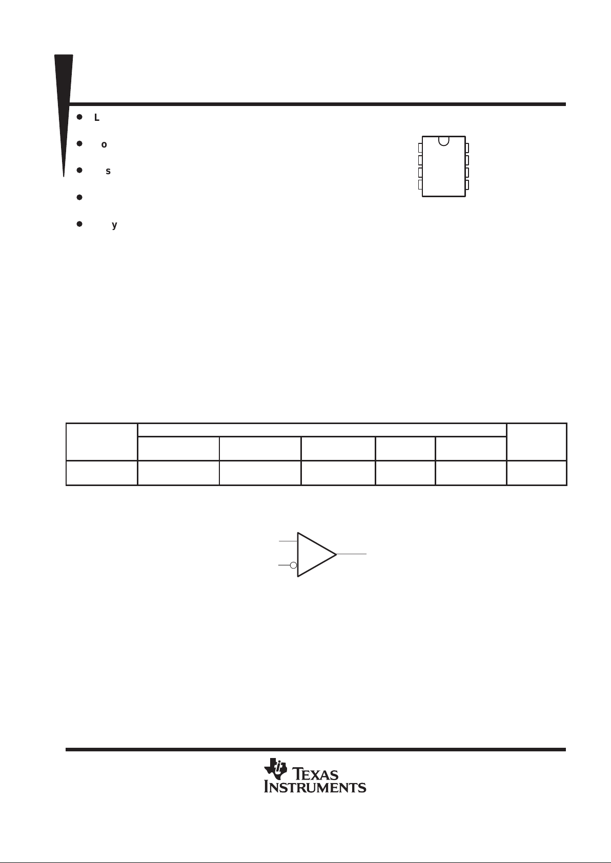
D, P, OR PW PACKAGE
(TOP VIEW)
TLV1393, TLV1393Y, TLV2393, TLV2393Y
DUAL DIFFERENTIAL COMPARATORS
SLCS121A – AUGUST 1993 – REVISED APRIL 1994
2
POST OFFICE BOX 655303 • DALLAS, TEXAS 75265
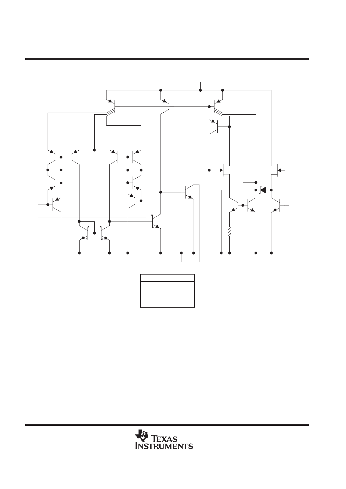
TLV1393, TLV1393Y equivalent schematic (each comparator)
V
CC
GND OUT
IN +
IN –
COMPONENT COUNT
Transistors 44
Resistors 1
Diodes
7
Epi-FET 2
TLV1393, TLV1393Y, TLV2393, TLV2393Y
DUAL DIFFERENTIAL COMPARATORS
SLCS121A – AUGUST 1993 – REVISED APRIL 1994
3
POST OFFICE BOX 655303 • DALLAS, TEXAS 75265
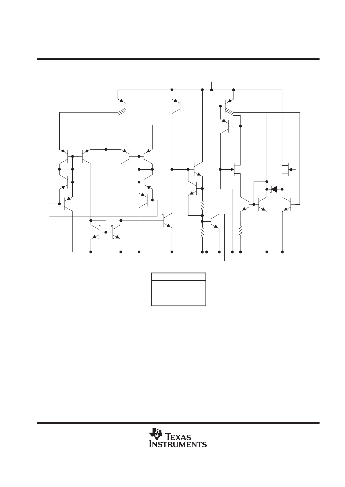
TLV2393, TLV2393Y equivalent schematic (each comparator)
V
CC
GND OUT
IN +
IN –
COMPONENT COUNT
Transistors 44
Resistors 1
Diodes
7
Epi-FET 2
TLV1393, TLV1393Y, TLV2393, TLV2393Y
DUAL DIFFERENTIAL COMPARATORS
SLCS121A – AUGUST 1993 – REVISED APRIL 1994
4
POST OFFICE BOX 655303 • DALLAS, TEXAS 75265
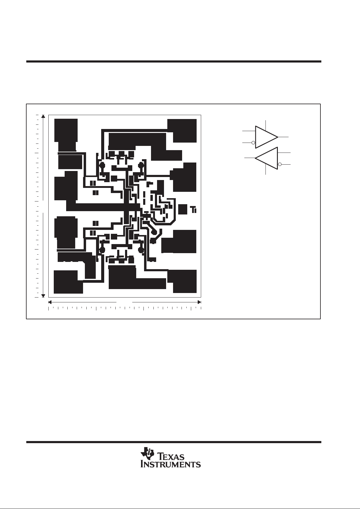
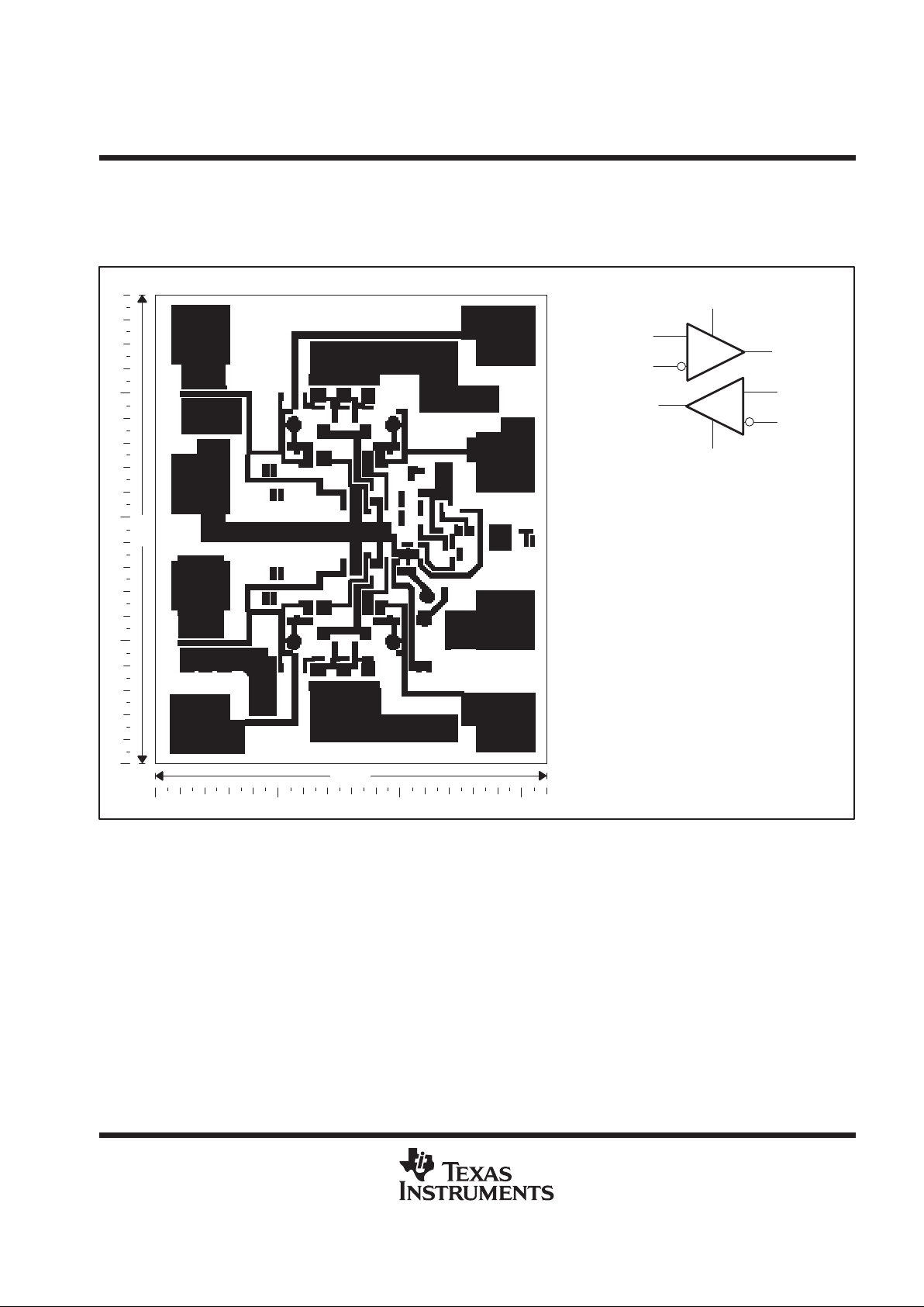
TLV1393Y chip information
This chip, when properly assembled, displays characteristics similar to the TL V1393. Thermal compression or
ultrasonic bonding may be used on the doped-aluminum bonding pads. Chips may be mounted with conductive
epoxy or a gold-silicon preform.
BONDING PAD ASSIGNMENTS
CHIP THICKNESS: 13 TYPICAL
BONDING PADS: 3.54 × 3.54 MINIMUM
TJmax = 150°C
TOLERANCES ARE ±10%.
ALL DIMENSIONS ARE IN MILS.
PIN (4) IS INTERNALLY CONNECTED
TO BACKSIDE OF CHIP.
+
–
1OUT
1IN+
1IN–
V
CC
(8)
(6)
(3)
(2)
(5)
(1)
–
+
(7)
2IN+
2IN–
2OUT
(4)
GND
32
38
(1)
(2)
(3)
(4)
(5)
(6)(7)
(8)
TLV1393, TLV1393Y, TLV2393, TLV2393Y
DUAL DIFFERENTIAL COMPARATORS
SLCS121A – AUGUST 1993 – REVISED APRIL 1994
5
POST OFFICE BOX 655303 • DALLAS, TEXAS 75265
TLV2393Y chip information
This chip, when properly assembled, displays characteristics similar to the TL V2393. Thermal compression or
ultrasonic bonding may be used on the doped-aluminum bonding pads. Chips may be mounted with conductive
epoxy or a gold-silicon preform.
BONDING PAD ASSIGNMENTS
CHIP THICKNESS: 15 TYPICAL
BONDING PADS: 3.6 × 3.6 MINIMUM
TJmax = 150°C
TOLERANCES ARE ±10%.
ALL DIMENSIONS ARE IN MILS.
PIN (4) IS INTERNALLY CONNECTED
TO BACKSIDE OF CHIP.
+
–
1OUT
1IN+
1IN–
V
CC
(8)
(6)
(3)
(2)
(5)
(1)
–
+
(7)
2IN+
2IN–
2OUT
(4)
GND
32
38
(1)
(2)
(3)
(4)
(5)
(6)(7)
(8)

TLV1393, TLV1393Y, TLV2393, TLV2393Y
DUAL DIFFERENTIAL COMPARATORS
SLCS121A – AUGUST 1993 – REVISED APRIL 1994
6
POST OFFICE BOX 655303 • DALLAS, TEXAS 75265
absolute maximum ratings over operating free-air temperature range (unless otherwise noted)
†
Supply voltage, V
CC
(see Note 1) 7 V. . . . . . . . . . . . . . . . . . . . . . . . . . . . . . . . . . . . . . . . . . . . . . . . . . . . . . . . . . . . .
Differential input voltage, V
ID
(see Note 2) 7 V. . . . . . . . . . . . . . . . . . . . . . . . . . . . . . . . . . . . . . . . . . . . . . . . . . . . .
Input voltage, V
I
(any input) 7 V. . . . . . . . . . . . . . . . . . . . . . . . . . . . . . . . . . . . . . . . . . . . . . . . . . . . . . . . . . . . . . . . . .
Output voltage, V
O
7 V. . . . . . . . . . . . . . . . . . . . . . . . . . . . . . . . . . . . . . . . . . . . . . . . . . . . . . . . . . . . . . . . . . . . . . . . . .
Output current, I
O
(each output) 20 mA. . . . . . . . . . . . . . . . . . . . . . . . . . . . . . . . . . . . . . . . . . . . . . . . . . . . . . . . . . .
Duration of short-circuit current to GND (see Note 3) unlimited. . . . . . . . . . . . . . . . . . . . . . . . . . . . . . . . . . . . . . .
Continuous total dissipation See Dissipation Rating Table. . . . . . . . . . . . . . . . . . . . . . . . . . . . . . . . . . . . . . . . . . .
Operating free-air temperature range, T
A
–40°C to 105°C. . . . . . . . . . . . . . . . . . . . . . . . . . . . . . . . . . . . . . . . . . .
Storage temperature range –65°C to 150°C. . . . . . . . . . . . . . . . . . . . . . . . . . . . . . . . . . . . . . . . . . . . . . . . . . . . . . . .
Lead temperature 1,6 mm (1/16 inch) from case for 10 seconds 260°C. . . . . . . . . . . . . . . . . . . . . . . . . . . . . . .
†
Stresses beyond those listed under “absolute maximum ratings” may cause permanent damage to the device. These are stress ratings only, and
functional operation of the device at these or any other conditions beyond those indicated under “recommended operating conditions” is not
implied. Exposure to absolute-maximum-rated conditions for extended periods may affect device reliability.
NOTES: 1. All voltage values, except differential voltages, are with respect to the network GND.
2. Differential voltages are at the noninverting input with respect to the inverting input.
3. Short circuits from the outputs to VCC can cause excessive heating and eventual destruction of the chip.
DISSIPATION RATING TABLE
PACKAGE
TA ≤ 25°C
POWER RATING
DERATING FACTOR
ABOVE TA = 25°C
TA = 70°C
POWER RATING
TA = 85°C
POWER RATING
D 725 mW 5.8 mW/°C 464 mW 377 mW
P 1000 mW 8.0 mW/°C 640 mW 520 mW
PW 525 mW 4.2 mW/°C 336 mW 273 mW
recommended operating conditions
MIN MAX
UNIT
Supply voltage, V
CC
2 7 V
Operating free-air temperature, T
A
–40 105 °C

TLV1393, TLV1393Y, TLV2393, TLV2393Y
DUAL DIFFERENTIAL COMPARATORS
SLCS121A – AUGUST 1993 – REVISED APRIL 1994
7
POST OFFICE BOX 655303 • DALLAS, TEXAS 75265
electrical characteristics, VCC = 3 V
TLV1393
PARAMETER
TEST CONDITIONS
T
A
†
MIN TYP MAX
UNIT
p
25°C 1.5 5
VIOInput offset voltage
V
O
= 1.4 V,
V
IC
=
V
ICR
min
Full range 120 9
mV
p
25°C
0 to
VCC – 1.5
0 to
VCC –1.2
V
ICR
Common-mode input voltage range
Full range
0 to
VCC –2
V
V
OL
Low-level output voltage VID = –1 V, IOL = 500 µA Full range 120 300 mV
p
25°C 5 50
IIOInput offset current
V
O
=
1.4 V
Full range 150
nA
p
25°C –40 –250
IIBInput bias current
V
O
= 1.4
V
Full range –400
nA
p
VID = 1 V, VOH = 3 V 25°C 0.1
IOHHigh-level output current
VID = 1 V, VOH = 5 V Full range 100
nA
I
OL
Low-level output current VID = –1 V, VOL = 1.5 V 25°C 500 µA
pp
25°C 160 250
I
CCH
High-level supply current
V
O
=
V
OH
Full range 300
pp
25°C 160 250
µ
A
I
CCL
Low-level supply current
V
O
=
V
OL
Full range 300
†
Full range is –40°C to 105°C.
switching characteristics, VCC = 3 V, CL = 15 pF, T
A
= 25°C
TLV1393
PARAMETER
TEST CONDITIONS
MIN TYP MAX
UNIT
Response time
100-mV input step with 5-mV overdrive, RL connected to 5 V through 5.1 kΩ
0.7 µs

TLV1393, TLV1393Y, TLV2393, TLV2393Y
DUAL DIFFERENTIAL COMPARATORS
SLCS121A – AUGUST 1993 – REVISED APRIL 1994
8
POST OFFICE BOX 655303 • DALLAS, TEXAS 75265
electrical characteristics, VCC = 5 V
TLV1393
PARAMETER
TEST CONDITIONS
T
A
†
MIN TYP MAX
UNIT
p
25°C 1.5 5
VIOInput offset voltage
V
O
= 1.4 V,
V
IC
=
V
ICR
min
Full range 9
mV
p
25°C
0 to
VCC – 1.5
0 to
VCC –1.2
V
ICR
Common-mode input voltage range
Full range
0 to
VCC –2
V
V
OL
Low-level output voltage VID = –1 V, IOL = 500 µA Full range 120 300 mV
p
25°C 5 50
IIOInput offset current
V
O
=
1.4 V
Full range 150
nA
p
25°C –40 –250
IIBInput bias current
V
O
= 1.4
V
Full range –400
nA
p
VID = 1 V, VOH = 3 V 25°C 0.1
IOHHigh-level output current
VID = 1 V, VOH = 5 V Full range 100
nA
I
OL
Low-level output current VID = –1 V, VOL = 1.5 V 25°C 600 µA
pp
25°C 200 300
I
CCH
High-level supply current
V
O
=
V
OH
Full range 350
pp
25°C 200 300
µ
A
I
CCL
Low-level supply current
V
O
=
V
OL
Full range 350
†
Full range is –40°C to 105°C.
switching characteristics, VCC = 5 V, CL = 15 pF, T
A
= 25°C
TLV1393
PARAMETER
TEST CONDITIONS
MIN TYP MAX
UNIT
p
100-mV input step with 5-mV overdrive, RL connected to 5 V through 5.1 kΩ 0.65
Response time
TTL-level input step, RL connected to 5 V through 5.1 kΩ
0.18
µ
s
electrical characteristics, VCC = 3 V, T
A
= 25°C
TLV1393Y
PARAMETER
TEST CONDITIONS
MIN TYP MAX
UNIT
V
IO
Input offset voltage VO = 1.4 V, VIC = V
ICR
min 1.5 5 mV
V
ICR
Common-mode input voltage range
0 to
VCC – 1.5
0 to
VCC –1.2
V
I
IO
Input offset current VO = 1.4 V 5 50 nA
I
IB
Input bias current VO = 1.4 V –40 –250 nA
I
OH
High-level output current VID = 1 V, VOH = 3 V 0.1 nA
I
OL
Low-level output current VID = –1 V, VOL = 1.5 V 500 µA
I
CCH
High-level supply current VO = V
OH
160 250
I
CCL
Low-level supply current
VO = V
OL
160 250
µ
A
switching characteristics, VCC = 3 V, CL = 15 pF, T
A
= 25°C
TLV1393Y
PARAMETER
TEST CONDITIONS
MIN TYP MAX
UNIT
Response time 100-mV input step with 5-mV overdrive, RL connected to 5 V through 5.1 kΩ 0.7 µs
TLV1393, TLV1393Y, TLV2393, TLV2393Y
DUAL DIFFERENTIAL COMPARATORS
SLCS121A – AUGUST 1993 – REVISED APRIL 1994
9
POST OFFICE BOX 655303 • DALLAS, TEXAS 75265
electrical characteristics, VCC = 5 V, T
A
= 25°C
TLV1393Y
PARAMETER
TEST CONDITIONS
MIN TYP MAX
UNIT
V
IO
Input offset voltage VO = 1.4 V, VIC = V
ICR
min 1.5 5 mV
V
ICR
Common-mode input voltage range
0 to
VCC – 1.5
0 to
VCC –1.2
V
I
IO
Input offset current VO = 1.4 V 5 50 nA
I
IB
Input bias current VO = 1.4 V –40 –250 nA
I
OH
High-level output current VID = 1 V, VOH = 3 V 0.1 nA
I
OL
Low-level output current VID = –1 V, VOL = 1.5 V 600 µA
I
CCH
High-level supply current VO = V
OH
200 300
I
CCL
Low-level supply current
VO = V
OL
200 300
µ
A
switching characteristics, VCC = 5 V, CL = 15 pF, T
A
= 25°C
TLV1393Y
PARAMETER
TEST CONDITIONS
MIN TYP MAX
UNIT
p
100-mV input step with 5-mV overdrive, RL connected to 5 V through 5.1 kΩ 0.65
Response time
TTL-level input step, RL connected to 5 V through 5.1 kΩ
0.18
µ
s

TLV1393, TLV1393Y, TLV2393, TLV2393Y
DUAL DIFFERENTIAL COMPARATORS
SLCS121A – AUGUST 1993 – REVISED APRIL 1994
10
POST OFFICE BOX 655303 • DALLAS, TEXAS 75265
electrical characteristics, VCC = 3 V
TLV2393
PARAMETER
TEST CONDITIONS
T
A
†
MIN TYP MAX
UNIT
p
25°C 1.5 5
VIOInput offset voltage
V
O
= 1.4 V,
V
IC
=
V
ICR
min
Full range 9
mV
p
25°C
0 to
VCC – 1.5
0 to
VCC –1.2
V
ICR
Common-mode input voltage range
Full range
0 to
VCC –2
V
p
VID = –1 V, IOL = 1 mA 25°C 80 300
VOLLow-level output voltage
VID = –1 V, IOL = 4 mA Full range 250 700
mV
p
25°C 5 50
IIOInput offset current
V
O
=
1.4 V
Full range 150
nA
p
25°C –100 –250
IIBInput bias current
V
O
= 1.4
V
Full range –400
nA
p
VID = 1 V, VOH = 3 V 25°C 0.1
IOHHigh-level output current
VID = 1 V, VOH = 5 V Full range 100
nA
I
OL
Low-level output current VID = –1 V, VOL = 1.5 V 25°C 4 mA
pp
25°C 450 600
I
CCH
High-level supply current
V
O
=
V
OH
Full range 700
µ
A
pp
25°C 1.1 1.3
I
CCL
Low-level supply current
V
O
=
V
OL
Full range 1.4
mA
†
Full range is –40°C to 105°C.
switching characteristics, VCC = 3 V, CL = 15 pF, T
A
= 25°C
TLV2393
PARAMETER
TEST CONDITIONS
MIN TYP MAX
UNIT
Response time
100-mV input step with 5-mV overdrive, RL connected to 5 V through 5.1 kΩ
0.45 1 µs

TLV1393, TLV1393Y, TLV2393, TLV2393Y
DUAL DIFFERENTIAL COMPARATORS
SLCS121A – AUGUST 1993 – REVISED APRIL 1994
11
POST OFFICE BOX 655303 • DALLAS, TEXAS 75265
electrical characteristics, VCC = 5 V
TLV2393
PARAMETER
TEST CONDITIONS
T
A
†
MIN TYP MAX
UNIT
p
25°C 1.5 5
VIOInput offset voltage
V
O
= 1.4 V,
V
IC
=
V
ICR
min
Full range 9
mV
p
25°C
0 to
VCC – 1.5
0 to
VCC –1.2
V
ICR
Common-mode input voltage range
Full range
0 to
VCC –2
V
p
VID = –1 V, IOL = 1 mA 25°C 70 300
VOLLow-level output voltage
VID = –1 V, IOL = 4 mA Full range 200 700
mV
p
25°C 5 50
IIOInput offset current
V
O
=
1.4 V
Full range 150
nA
p
25°C –100 –250
IIBInput bias current
V
O
= 1.4
V
Full range –400
nA
p
VID = 1 V, VOH = 3 V 25°C 0.1
IOHHigh-level output current
VID = 1 V, VOH = 5 V Full range 100
nA
I
OL
Low-level output current VID = –1 V, VOL = 1.5 V 25°C 6 mA
pp
25°C 550 700
I
CCH
High-level supply current
V
O
=
V
OH
Full range 800
µ
A
pp
25°C 1.2 1.5
I
CCL
Low-level supply current
V
O
=
V
OL
Full range 1.6
mA
†
Full range is –40°C to 105°C.
switching characteristics, VCC = 5 V, CL = 15 pF, T
A
= 25°C
TLV2393
PARAMETER
TEST CONDITIONS
MIN TYP MAX
UNIT
p
100-mV input step with 5-mV overdrive, RL connected to 5 V through 5.1 kΩ 0.4 0.8
Response time
TTL-level input step, RL connected to 5 V through 5.1 kΩ
0.15 0.3
µ
s

TLV1393, TLV1393Y, TLV2393, TLV2393Y
DUAL DIFFERENTIAL COMPARATORS
SLCS121A – AUGUST 1993 – REVISED APRIL 1994
12
POST OFFICE BOX 655303 • DALLAS, TEXAS 75265
electrical characteristics, VCC = 3 V, T
A
= 25°C
TLV2393Y
PARAMETER
TEST CONDITIONS
MIN TYP MAX
UNIT
V
IO
Input offset voltage VO = 1.4 V, VIC = V
ICR
min 1.5 5 mV
V
ICR
Common-mode input voltage range
0 to
VCC – 1.5
0 to
VCC –1.2
V
V
OL
Low-level output voltage VID = –1 V, IOL = 1 mA 80 300 mV
I
IO
Input offset current VO = 1.4 V 5 50 nA
I
IB
Input bias current VO = 1.4 V –100 –250 nA
I
OH
High-level output current VID = 1 V, VOH = 3 V 0.1 nA
I
OL
Low-level output current VID = –1 V, VOL = 1.5 V 4 mA
I
CCH
High-level supply current VO = V
OH
450 600 µA
I
CCL
Low-level supply current
VO = V
OL
1.1 1.3 mA
switching characteristics, VCC = 3 V, CL = 15 pF, T
A
= 25°C
TLV2393Y
PARAMETER
TEST CONDITIONS
MIN TYP MAX
UNIT
Response time
100-mV input step with 5-mV overdrive, RL connected to 5 V through 5.1 kΩ
0.45 1 µs
electrical characteristics, VCC = 5 V, T
A
= 25°C
TLV2393Y
PARAMETER
TEST CONDITIONS
MIN TYP MAX
UNIT
V
IO
Input offset voltage VO = 1.4 V, VIC = V
ICR
min 1.5 5 mV
V
ICR
Common-mode input voltage range
0 to
VCC – 1.5
0 to
VCC –1.2
V
V
OL
Low-level output voltage VID = –1 V, IOL = 1 mA 70 300 mV
I
IO
Input offset current VO = 1.4 V 5 50 nA
I
IB
Input bias current VO = 1.4 V –100 –250 nA
I
OH
High-level output current VID = 1 V, VOH = 3 V 0.1 nA
I
OL
Low-level output current VID = –1 V, VOL = 1.5 V 6 mA
I
CCH
High-level supply current VO = V
OH
550 700 µA
I
CCL
Low-level supply current
VO = V
OL
1.2 1.5 mA
switching characteristics, VCC = 5 V, CL = 15 pF, T
A
= 25°C
TLV2393Y
PARAMETER
TEST CONDITIONS
MIN TYP MAX
UNIT
p
100-mV input step with 5-mV overdrive, RL connected to 5 V through 5.1 kΩ 0.4 0.8
Response time
TTL-level input step, RL connected to 5 V through 5.1 kΩ
0.15 0.3
µ
s

TLV1393, TLV1393Y, TLV2393, TLV2393Y
DUAL DIFFERENTIAL COMPARATORS
SLCS121A – AUGUST 1993 – REVISED APRIL 1994
13
POST OFFICE BOX 655303 • DALLAS, TEXAS 75265
TYPICAL CHARACTERISTICS
Table of Graphs
FIGURE
p
vs Low-to-high-level output response time 1, 3
Input overdrives for TLV1393
vs High-to-low-level output response time 2, 4
p
vs Low-to-high-level output response time 5, 7
Input overdrives for TLV2393
vs High-to-low-level output response time 6, 8
Figure 1
0 0.5 1 1.5 2 2.5
TLV1393 LOW-TO HIGH-LEVEL OUTPUT
RESPONSE FOR VARIOUS INPUT OVERDRIVES
Low-to High-Level Output Response Time – µs
VCC = 3 V
TA = 25° C
3
0
100
0
40 mV
20 mV
10 mV
5 mV
2 mV
– Output Voltage – VV
O
V
ID
– Differential
Input Voltage – mV
Figure 2
40 mV
20 mV
10 mV
5 mV
2 mV
TLV1393 HIGH-TO LOW-LEVEL OUTPUT
RESPONSE FOR VARIOUS INPUT OVERDRIVES
High-to Low-Level Output Response Time – µs
3
0
100
0
0 0.2 0.4 0.6 0.8
VCC = 3 V
TA = 25° C
– Output Voltage – VV
O
V
ID
– Differential
Input Voltage – mV

TLV1393, TLV1393Y, TLV2393, TLV2393Y
DUAL DIFFERENTIAL COMPARATORS
SLCS121A – AUGUST 1993 – REVISED APRIL 1994
14
POST OFFICE BOX 655303 • DALLAS, TEXAS 75265
TYPICAL CHARACTERISTICS
Figure 3
0 0.5 1 1.5 2 2.5
TLV1393 LOW-TO HIGH-LEVEL OUTPUT
RESPONSE FOR VARIOUS INPUT OVERDRIVES
Low-to High-Level Output Response Time – µs
VCC = 5 V
TA = 25° C
5
0
100
0
40 mV
20 mV
10 mV
5 mV
2 mV
– Output Voltage – VV
O
V
ID
– Differential
Input Voltage – mV
Figure 4
40 mV
20 mV
10 mV
5 mV
2 mV
TLV1393 HIGH-TO LOW-LEVEL OUTPUT
RESPONSE FOR VARIOUS INPUT OVERDRIVES
High-to Low-Level Output Response Time – µs
5
0
100
0
0 0.2 0.4 0.6 0.8
VCC = 5 V
TA = 25° C
– Output Voltage – VV
O
V
ID
– Differential
Input Voltage – mV
Figure 5
0 0.2 0.4 0.6 0.8 1
TLV2393 LOW-TO HIGH-LEVEL OUTPUT
RESPONSE FOR VARIOUS INPUT OVERDRIVES
Low-to High-Level Output Response Time – µs
VCC = 3 V
TA = 25° C
3
0
100
0
40 mV
20 mV
10 mV
5 mV
2 mV
– Output Voltage – VV
O
V
ID
– Differential
Input Voltage – mV
Figure 6
40 mV
20 mV
10 mV
5 mV
2 mV
TLV2393 HIGH-TO LOW-LEVEL OUTPUT
RESPONSE FOR VARIOUS INPUT OVERDRIVES
High-to Low-Level Output Response Time – µs
3
0
100
0
0 0.1 0.2 0.3 0.4
VCC = 3 V
TA = 25° C
– Output Voltage – VV
O
V
ID
– Differential
Input Voltage – mV

TLV1393, TLV1393Y, TLV2393, TLV2393Y
DUAL DIFFERENTIAL COMPARATORS
SLCS121A – AUGUST 1993 – REVISED APRIL 1994
15
POST OFFICE BOX 655303 • DALLAS, TEXAS 75265
TYPICAL CHARACTERISTICS
Figure 7
0 0.2 0.4 0.6 0.8 1
TLV2393 LOW-TO HIGH-LEVEL OUTPUT
RESPONSE FOR VARIOUS INPUT OVERDRIVES
Low-to High-Level Output Response Time – µs
VCC = 5 V
TA = 25° C
5
0
100
0
40 mV
20 mV
10 mV
5 mV
2 mV
– Output Voltage – VV
O
V
ID
– Differential
Input Voltage – mV
Figure 8
40 mV
20 mV
10 mV
5 mV
2 mV
TLV2393 HIGH-TO LOW-LEVEL OUTPUT
RESPONSE FOR VARIOUS INPUT OVERDRIVES
High-to Low-Level Output Response Time – µs
5
0
100
0
0 0.1 0.2 0.3 0.4
VCC = 5 V
TA = 25° C
– Output Voltage – VV
O
V
ID
– Differential
Input Voltage – mV

IMPORTANT NOTICE
T exas Instruments and its subsidiaries (TI) reserve the right to make changes to their products or to discontinue
any product or service without notice, and advise customers to obtain the latest version of relevant information
to verify, before placing orders, that information being relied on is current and complete. All products are sold
subject to the terms and conditions of sale supplied at the time of order acknowledgement, including those
pertaining to warranty, patent infringement, and limitation of liability.
TI warrants performance of its semiconductor products to the specifications applicable at the time of sale in
accordance with TI’s standard warranty. Testing and other quality control techniques are utilized to the extent
TI deems necessary to support this warranty. Specific testing of all parameters of each device is not necessarily
performed, except those mandated by government requirements.
CERT AIN APPLICATIONS USING SEMICONDUCTOR PRODUCTS MAY INVOLVE POTENTIAL RISKS OF
DEATH, PERSONAL INJURY, OR SEVERE PROPERTY OR ENVIRONMENTAL DAMAGE (“CRITICAL
APPLICATIONS”). TI SEMICONDUCTOR PRODUCTS ARE NOT DESIGNED, AUTHORIZED, OR
WARRANTED TO BE SUITABLE FOR USE IN LIFE-SUPPORT DEVICES OR SYSTEMS OR OTHER
CRITICAL APPLICATIONS. INCLUSION OF TI PRODUCTS IN SUCH APPLICA TIONS IS UNDERST OOD TO
BE FULLY AT THE CUSTOMER’S RISK.
In order to minimize risks associated with the customer’s applications, adequate design and operating
safeguards must be provided by the customer to minimize inherent or procedural hazards.
TI assumes no liability for applications assistance or customer product design. TI does not warrant or represent
that any license, either express or implied, is granted under any patent right, copyright, mask work right, or other
intellectual property right of TI covering or relating to any combination, machine, or process in which such
semiconductor products or services might be or are used. TI’s publication of information regarding any third
party’s products or services does not constitute TI’s approval, warranty or endorsement thereof.
Copyright 1998, Texas Instruments Incorporated
 Loading...