

Texas Instruments TLV2352MUB, TLV2352MJGB, TLV2352MJG, TLV2352MFKB, TLV2352IPWR Datasheet
...
LinCMOS DUAL LOW-VOLTAGE DIFFERENTIAL COMPARATORS
CHIP
TLV2352Y
D
Wide Range of Supply Voltages
2 V to 8 V
D
Fully Characterized at 3 V and 5 V
D
Very-Low Supply-Current Drain
120 µA Typ at 3 V
D
Output Compatible With TTL, MOS, and
CMOS
D
Fast Response Time . . . 200 ns Typ for
TTL-Level Input Step
description
TLV2352, TLV2352Y
SLCS01 1B – MAY 1992 – REVISED MARCH 1999
D
High Input Impedance ...1012 Ω Typ
D
Extremely Low Input Bias Current
5 pA Typ
D
Common-Mode Input Voltage Range
Includes Ground
D
Built-In ESD Protection
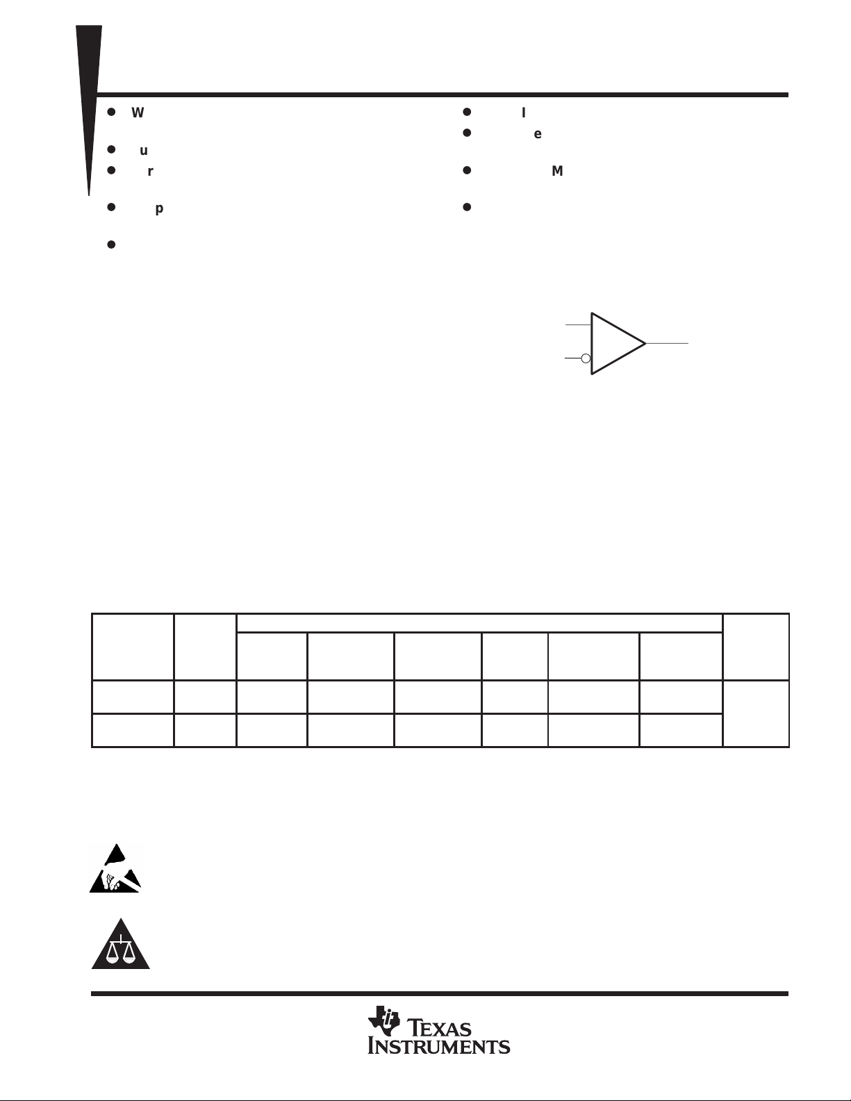
symbol (each comparator)
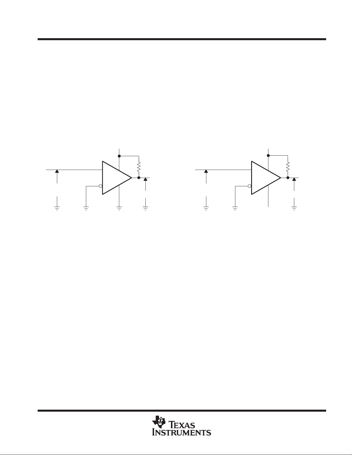
The TLV2352 consists of two independent,
low-power comparators specifically designed for
single power-supply applications and operates
IN+
OUT
IN–
with power-supply rails as low as 2 V. When
powered from a 3-V supply, the typical supply
current is only 120 µA.
The TLV2352 is designed using the Texas Instruments LinCMOS technology and therefore features an
extremely high input impedance (typically greater than 1012 Ω), which allows direct interfacing with
high-impedance sources. The outputs are N-channel open-drain configurations that require an external pullup
resistor to provide a positive output voltage swing, and they can be connected to achieve positive-logic
wired-AND relationships. The TL V2352I is fully characterized at 3 V and 5 V for operation from – 40°C to 85°C.
The TLV2352M is fully characterized at 3 V and 5 V for operation from – 55°C to 125°C.
The TLV2352 has internal electrostatic-discharge (ESD)-protection circuits and has been classified with a
1000-V ESD rating using Human Body Model testing. However, care should be exercised in handling this device
as exposure to ESD may result in degradation of the device parametric performance.
AVAILABLE OPTIONS
PACKAGED DEVICES
T
A
–40°C to
85°C
–55°C to
125°C
†
The D package is available taped and reeled. Add the suffix R to the device type (e.g., TL V2352IDR).
‡
The PW packages are only available left-ended taped and reeled (e.g., TLV2352IPWLE)
VIO max
at 25°C
5 mV TLV2352ID — — TLV2352IP TLV2352IPWLE —
5 mV — TLV2352MFK TLV2352MJG — — TLV2352MU
SMALL
OUTLINE
†
(D)
CHIP
CARRIER
(FK)
CERAMIC
DIP
(JG)
PLASTIC
DIP
(P)
TSSOP
(PW)
PLASTIC
‡
DIP
(U)
FORM
(Y)
These devices have limited built-in protection. The leads should be shorted together or the device placed in conductive foam during
storage or handling to prevent electrostatic damage to the MOS gates.
Please be aware that an important notice concerning availability, standard warranty, and use in critical applications of
Texas Instruments semiconductor products and disclaimers thereto appears at the end of this data sheet.
LinCMOS is a trademark of Texas Instruments Incorporated.
PRODUCTION DATA information is current as of publication date.
Products conform to specifications per the terms of Texas Instruments
standard warranty. Production processing does not necessarily include
testing of all parameters.
POST OFFICE BOX 655303 • DALLAS, TEXAS 75265
Copyright 1999, Texas Instruments Incorporated
On products compliant to MIL-PRF-38535, all parameters are tested
unless otherwise noted. On all other products, production
processing does not necessarily include testing of all parameters.
1
TLV2352, TLV2352Y
LinCMOS DUAL LOW-VOLTAGE DIFFERENTIAL COMPARATORS
SLCS01 1B – MAY 1992 – REVISED MARCH 1999
TLV2352I...D OR P PACKAGE
TLV2352M. . . JG PACKAGE
(TOP VIEW)
V
DD–
1OUT
1IN–
1IN+
/GND
1
2
3
4
8
7
6
5
V
DD+
2OUT
2IN–
2IN+
V
DD–
NC
1IN–
NC
1IN+
NC
TLV2254M
U PACKAGE
(TOP VIEW)
1
•
NC
1OUT
1IN–
1IN+
/GND
2
3
4
5
TLV2352M
FK PACKAGE
(TOP VIEW)
NC
1OUT
3212019
4
5
6
7
8
910111213
NC
10
9
8
7
6
DD+
V
NC
18
17
16
15
14
NC
V
DD+
2OUT
2IN–
2IN+
NC
2OUT
NC
2IN–
NC
TLV2352I. . . PW PACKAGE
(TOP VIEW)
1OUT
1IN–
1IN+
V
/GND
DD–
NC – No internal connection
1
2
3
4
8
7
6
5
V
DD+
2OUT
2IN–
2IN+
NC
NC
/GND
DD –
V
2IN+
NC
2
POST OFFICE BOX 655303 • DALLAS, TEXAS 75265
LinCMOS
OUT
TLV2352, TLV2352Y
DUAL LOW-VOLTAGE DIFFERENTIAL COMPARATORS
SLCS01 1B – MAY 1992 – REVISED MARCH 1999
Common to All Channels
IN–
IN+
DD
equivalent schematic
V
GND
POST OFFICE BOX 655303 DALLAS, TEXAS 75265
• 3
TLV2352, TLV2352Y
LinCMOS DUAL LOW-VOLTAGE DIFFERENTIAL COMPARATORS
SLCS01 1B – MAY 1992 – REVISED MARCH 1999
TLV2352Y chip information
These chips, when properly assembled, display characteristics similar to the TL V2352. Thermal compression
or ultrasonic bonding may be used on the doped-aluminum bonding pads. This chip can be mounted with
conductive epoxy or a gold-silicon preform.
BONDING PAD ASSIGNMENTS
57
(7)
(8)
57
(6)
(3)(2)(1)
(5)
(4)
V
DD
+
–
GND
(8)
(4)
(1)
(5)
+
(6)
–
(3)
IN+
(2)
IN–
(7)
OUT
CHIP THICKNESS: 15 MILS TYPICAL
BONDING PADS: 4 × 4 MILS MINIMUM
TJmax = 150°C
TOLERANCES ARE ±10%.
ALL DIMENSIONS ARE IN MILS.
PIN (4) INTERNALLY CONNECTED
TO BACKSIDE OF CHIP.
OUT
IN+
IN–
4
POST OFFICE BOX 655303 • DALLAS, TEXAS 75265
TLV2352, TLV2352Y
Common-mode input voltage, V
V
O erating free-air tem erature, T
A
°C
LinCMOS DUAL LOW-VOLTAGE DIFFERENTIAL COMPARATORS
SLCS01 1B – MAY 1992 – REVISED MARCH 1999
absolute maximum ratings over operating free-air temperature range (unless otherwise noted)
Supply voltage, VDD (see Note 1) 8 V. . . . . . . . . . . . . . . . . . . . . . . . . . . . . . . . . . . . . . . . . . . . . . . . . . . . . . . . . . . . .
Differential input voltage, VID (see Note 2) ±8 V. . . . . . . . . . . . . . . . . . . . . . . . . . . . . . . . . . . . . . . . . . . . . . . . . . . .
Input voltage range, V
Output voltage, VO 8 V. . . . . . . . . . . . . . . . . . . . . . . . . . . . . . . . . . . . . . . . . . . . . . . . . . . . . . . . . . . . . . . . . . . . . . . . . .
Input current, II ±5 mA. . . . . . . . . . . . . . . . . . . . . . . . . . . . . . . . . . . . . . . . . . . . . . . . . . . . . . . . . . . . . . . . . . . . . . . . . .
Output current, IO 20 mA. . . . . . . . . . . . . . . . . . . . . . . . . . . . . . . . . . . . . . . . . . . . . . . . . . . . . . . . . . . . . . . . . . . . . . .
Duration of output short-circuit current to GND (see Note 3) unlimited. . . . . . . . . . . . . . . . . . . . . . . . . . . . . . . . .
Continuous total power dissipation See Dissipation Rating Table. . . . . . . . . . . . . . . . . . . . . . . . . . . . . . . . . . . . .
Operating free-air temperature range, T
Storage temperature range, T
Lead temperature 1,6 mm (1/16 inch) from case for 10 seconds: D, P, and PW Packages 260°C. . . . . . . . .
Lead temperature 1,6 mm (1/16 inch) from case for 10 seconds: FK, JG, and U Packages 300°C. . . . . . . .
†
Stress beyond those listed under “absolute maximum ratings” may cause permanent damage to the device. These are stress ratings only, and
functional operation of the device at these or any other conditions beyond those indicated under “recommended operating conditions” is not
implied. Exposure to absolute-maximum-rated conditions for extended periods may affect device reliability.
NOTES: 1. All voltage values, except differential voltages, are with respect to network ground.
2. Differential voltages are at IN+ with respect to IN–.
3. Short circuits from outputs to VDD can cause excessive heating and eventual device destruction.
PACKAGE
–0.3 to 8 V. . . . . . . . . . . . . . . . . . . . . . . . . . . . . . . . . . . . . . . . . . . . . . . . . . . . . . . . . . . . . . . .
I
: TLV2352I –40°C to 85°C. . . . . . . . . . . . . . . . . . . . . . . . . . . . . . . . . . .
A
TLV2352M –55°C to 125°C. . . . . . . . . . . . . . . . . . . . . . . . . . . . . . . . .
–65°C to 150°C. . . . . . . . . . . . . . . . . . . . . . . . . . . . . . . . . . . . . . . . . . . . . . . . . . .
stg
DISSIPATION RATING TABLE
D
FK
JG
P
PW
U
TA ≤ 25°C
POWER RATING
725 mW
1375 mW
1050 mW
1000 mW
525 mW
700 mW
DERATING
FACTOR
5.8 mW/°C
11.0 mW/°C
8.4 mW/°C
8.0 mW/°C
4.2 mW/°C
5.5 mW/°C
TA = 85°C
POWER RATING
377 mW
715 mW
546 mW
520 mW
273 mW
370 mW
TA = 125°C
POWER RATING
275 mW
210 mW
150 mW
—
—
—
†
recommended operating conditions
Supply voltage, V
p
DD
p
IC
p
VDD = 3 V 0 1.75
VDD = 5 V 0 3.75
TLV2352I –40 85
TLV2352M –55 125
MIN MAX UNIT
2 8 V
°
POST OFFICE BOX 655303 • DALLAS, TEXAS 75265
5
TLV2352, TLV2352Y
VIOInput offset voltage
V
V
min
See Note 4
mV
IIOInput offset current
IIBInput bias current
Common-mode input
I
g
V
V
V
V
1 V
I
2 mA
mV
IDDSupply current
V
No load
A
PARAMETER
TEST CONDITIONS
UNIT
PARAMETER
TEST CONDITIONS
UNIT
Response time
R
C
F
§
See Note 5
ns
LinCMOS DUAL LOW-VOLTAGE DIFFERENTIAL COMPARATORS
SLCS01 1B – MAY 1992 – REVISED MARCH 1999
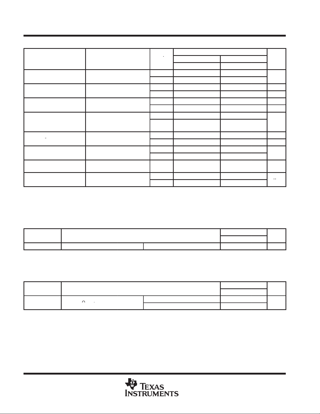
electrical characteristics at specified free-air temperature
PARAMETER TEST CONDITIONS
p
p
p
V
ICR
voltage range
High-level output
OH
current
Low-level output
OL
voltage
Low-level output
I
OL
current
pp
†
All characteristics are measured with zero common-mode input voltages unless otherwise noted.
‡
Full range is –40°C to 85°C. IMPORTANT: See
NOTE 4: The offset voltage limits given are the maximum values required to drive the output above 4 V with VDD = 5 V , 2 V with VDD = 3 V , or
below 400 mV with a 10-kΩ resistor between the output and VDD. They can be verified by applying the limit value to the input and
checking for the appropriate output state.
p
=
IC
= 1
ID
= –
ID
VID = –1 V, VOL = 1.5 V 25°C 6 16 6 16 mA
= 1 V,
ID
,
ICR
,
=
OL
Parameter Measurement Information
‡
T
A
25°C 1 5 1 5
Full range 7 7
25°C 1 1
85°C 1 1
25°C 5 5
85°C 2 2
25°C 0 to 2 0 to 4
Full range
25°C 0.1 0.1
Full range 1 1
25°C 115 300 150 400
Full range 600 700
25°C 120 250 140 300
Full range 350 400
†
TLV2352I
VDD = 3 V VDD = 5 V
MIN TYP MAX MIN TYP MAX
0 to
1.75
.
0 to
3.75
UNIT
pA
nA
pA
nA
V
nA
µA
µ
switching characteristics, V
Response time RL = 5.1 kΩ, CL = 15 pF§, See Note 5 100-mV input step with 5-mV overdrive 640 ns
§
CL includes probe and jig capacitance.
NOTE 5: The response time specified is the interval between the input step function and the instant when the output crosses VO = 1 V with
VDD = 3 V or VO = 1.4 V with VDD = 5 V.
= 3 V, T
DD
= 25°C
A
TLV2352I
MIN TYP MAX
switching characteristics, VDD = 5 V, TA = 25°C
TLV2352I
MIN TYP MAX
p
§
CL includes probe and jig capacitance.
NOTE 5: The response time specified is the interval between the input step function and the instant when the output crosses VO = 1 V with
VDD = 3 V or VO = 1.4 V with VDD = 5 V.
= 5.1 kΩ,
L
= 15 p
L
p
,
100-mV input step with 5-mV overdrive 650
TTL-level input step 200
6
POST OFFICE BOX 655303 • DALLAS, TEXAS 75265
TLV2352, TLV2352Y
VIOInput offset voltage
V
V
min
See Note 4
mV
IIOInput offset current
IIBInput bias current
Common-mode input
I
g
V
V
V
V
I
mA
mV
IDDSupply current
V
No load
A
PARAMETER
TEST CONDITIONS
UNIT
PARAMETER
TEST CONDITIONS
UNIT
Response time
R
C
100 pF
§
See Note 5
ns
LinCMOS DUAL LOW-VOLTAGE DIFFERENTIAL COMPARATORS
SLCS01 1B – MAY 1992 – REVISED MARCH 1999
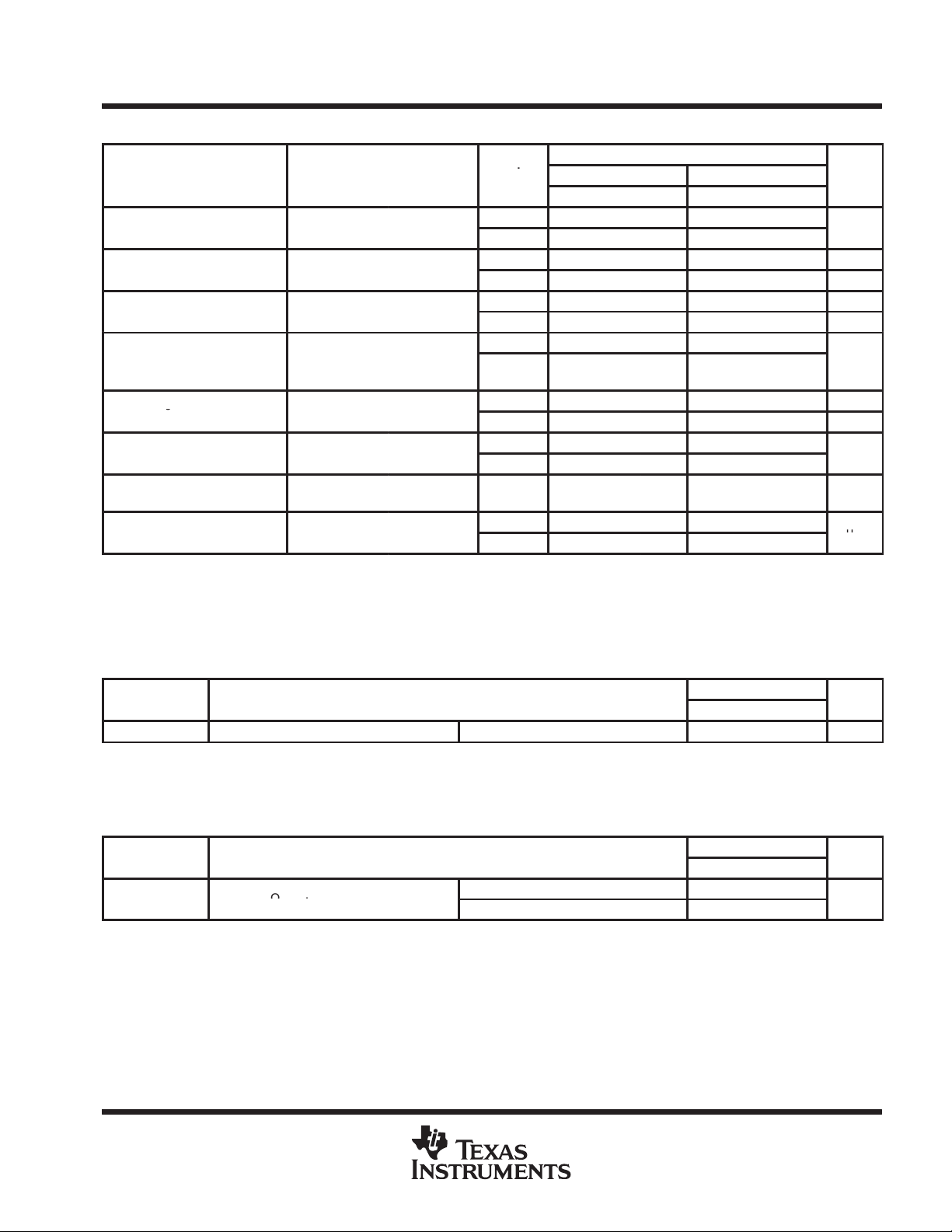
electrical characteristics at specified free-air temperature
PARAMETER TEST CONDITIONS
p
p
p
V
ICR
voltage range
High-level output
OH
current
Low-level output
OL
voltage
Low-level output
I
OL
current
pp
†
All characteristics are measured with zero common-mode input voltages unless otherwise noted.
‡
Full range is –55°C to 125°C. IMPORTANT: See
NOTE 4: The offset voltage limits given are the maximum values required to drive the output above 4 V with VDD = 5 V , 2 V with VDD = 3 V , or
below 400 mV with a 10-kΩ resistor between the output and VDD. They can be verified by applying the limit value to the input and
checking for the appropriate output state.
p
=
IC
= 1
ID
= –1 V,
ID
VID = –1 V, VOL = 1.5 V 25°C 6 16 6 16 mA
= 1 V,
ID
,
ICR
= 2
OL
Parameter Measurement Information
‡
T
A
25°C 1 5 1 5
Full range 10 10
25°C 1 1
125°C 10 10
25°C 5 5
125°C 20 20
25°C 0 to 2 0 to 4
Full range
25°C 0.1 0.1
Full range 1 1
25°C 115 300 150 400
Full range 600 700
25°C 120 250 140 300
Full range 350 400
†
TLV2352M
VDD = 3 V VDD = 5 V
MIN TYP MAX MIN TYP MAX
0 to
1.75
.
0 to
3.75
UNIT
pA
nA
pA
nA
V
nA
µA
µ
switching characteristics, V
Response time RL = 5.1 kΩ, CL = 100 pF§, See Note 5 100-mV input step with 5-mV overdrive 1400 ns
§
CL includes probe and jig capacitance.
NOTE 5: The response time specified is the interval between the input step function and the instant when the output crosses VO = 1 V with
VDD = 3 V or VO = 1.4 V with VDD = 5 V.
= 3 V, T
DD
= 25°C
A
TLV2352M
MIN TYP MAX
switching characteristics, VDD = 5 V, TA = 25°C
TLV2352M
MIN TYP MAX
p
§
CL includes probe and jig capacitance.
NOTE 5: The response time specified is the interval between the input step function and the instant when the output crosses VO = 1 V with
VDD = 3 V or VO = 1.4 V with VDD = 5 V.
= 5.1 kΩ,
L
p
=
L
,
100-mV input step with 5-mV overdrive 1300
TTL-level input step 900
POST OFFICE BOX 655303 • DALLAS, TEXAS 75265
7
TLV2352, TLV2352Y
LinCMOS DUAL LOW-VOLTAGE DIFFERENTIAL COMPARATORS
SLCS01 1B – MAY 1992 – REVISED MARCH 1999
electrical characteristics at specified free-air temperature, TA = 25°C
PARAMETER TEST CONDITIONS
V
I
I
V
I
V
I
I
†
NOTE 4: The offset voltage limits given are the maximum values required to drive the output above 4 V with VDD = 5 V , 2 V with VDD = 3 V , or
Input offset voltage VIC = V
IO
Input offset current 1 1 pA
IO
Input bias current 5 5 pA
IB
Common-mode input voltage range 0 to 2 0 to 4 V
ICR
High-level output current VID = 1 V 0.1 0.1 nA
OH
Low-level output voltage VID = –1 V, IOL = 2 mA 115 300 150 400 mV
OL
Low-level output current VID = –1 V, VOL = 1.5 V 6 16 6 16 mA
OL
Supply current VID = 1 V No load 120 250 140 300 µA
DD
All characteristics are measured with zero common-mode input voltages unless otherwise noted.
below 400 mV with a 10-kΩ resistor between the output and VDD. They can be verified by applying the limit value to the input and
checking for the appropriate output state.
min, See Note 4 1 5 1 5 mV
ICR
VDD = 3 V VDD = 5 V
MIN TYP MAX MIN TYP MAX
†
TLV2352Y
UNIT
8
POST OFFICE BOX 655303 • DALLAS, TEXAS 75265

TLV2352, TLV2352Y
LinCMOS DUAL LOW-VOLTAGE DIFFERENTIAL COMPARATORS
SLCS01 1B – MAY 1992 – REVISED MARCH 1999
TYPICAL CHARACTERISTICS
LOW-LEVEL OUTPUT VOLTAGE
vs
LOW-LEVEL OUTPUT CURRENT
1100
VDD = 3 V
990
TA = 25°C
880
770
660
550
440
330
– Low-Level Output Voltage – mV
220
OL
V
110
0
024681012
IOL – Low-Level Output Current – mA
Figure 1
COMMON-MODE INPUT VOLTAGE RANGE
vs
FREE-AIR TEMPERATURE
3
VDD = 3 V
2.5
2
1.5
Positive Limit
14 16
SUPPLY CURRENT
FREE-AIR TEMPERATURE
190
No Load
180
170
Aµ
160
150
140
VDD = 3 V
130
– Supply Current –
120
DD
I
110
100
90
–75 – 50 – 25 0 25 50 75
TA – Free-Air Temperature – °C
VDD = 5 V
Figure 2
OUTPUT FALL TIME
vs
CAPACITIVE LOAD
50
VDD = 3 V
45
Overdrive = 10 mV
RL = 5.1 kΩ (pullup to VDD)
40
TA = 25°C
35
30
vs
100 125
1
0.5
0
– Common-Mode Input Voltage Range – V
–0.5
ICR
V
–1
–75 –50 –25 0 25 50 75 100 125
TA – Free-Air Temperature – °C
Negative Limit
Figure 3
25
20
– Output Fall Time – ns
15
f
t
10
5
0
0 102030405060
POST OFFICE BOX 655303 • DALLAS, TEXAS 75265
70 80 90 100
CL – Capacitive Load – pF
Figure 4
9

TLV2352, TLV2352Y
LinCMOS DUAL LOW-VOLTAGE DIFFERENTIAL COMPARATORS
SLCS01 1B – MAY 1992 – REVISED MARCH 1999
TYPICAL CHARACTERISTICS
VDD = 3 V
CL = 15 pF
RL = 5.1 kΩ (pullup to VDD)
TA = 25°C
– Output
O
V
Voltage – V
0
100
0
– Differential
ID
V
Input Voltage – mV
HIGH-TO-LOW-LEVEL OUTPUT
PROPAGATION DELAY
FOR VARIOUS OVERDRIVE VOLTAGES
20 mV
0 100 200 300 400 500 6003700 800 900 1000
t
– High-to-Low-Level Output
PHL
Propagation Delay Time – ns
5 mV
10 mV
Figure 5
VDD = 3 V
Overdrive = 10 mV
RL = 5.1 kΩ (pullup to VDD)
TA = 25°C
– Output
O
V
Voltage – V
0
100
0
– Differential
ID
V
Input Voltage – mV
HIGH-TO-LOW-LEVEL OUTPUT
PROPAGATION DELAY
FOR VARIOUS CAPACITIVE LOADS
CL = 15 pF
0 100 200 300 400 500 6003700 800 900 1000
t
– High-to-Low-Level Output
PHL
Propagation Delay Time – ns
CL = 100 pF
CL = 50 pF
Figure 6
3
– Output
O
V
Voltage – V
0
100
0
– Differential
ID
V
Input Voltage – mV
LOW-TO-HIGH-LEVEL OUTPUT
PROPAGATION DELAY
FOR VARIOUS OVERDRIVE VOLTAGES
VDD = 3 V
CL = 15 pF
RL = 5.1 kΩ (pullup to VDD)
TA = 25°C
20 mV
5 mV
10 mV
0 100 200 300 400 500 600
t
– Low-to-High-Level Output
PLH
Propagation Delay Time – ns
700 800 900 1000
Figure 7
VDD = 3 V
Overdrive = 10 mV
RL = 5.1 kΩ (pullup to VDD)
TA = 25°C
– Output
O
V
Voltage – V
0
100
0
– Differential
ID
V
Input Voltage – mV
LOW-TO-HIGH-LEVEL OUTPUT
PROPAGATION DELAY
FOR VARIOUS CAPACITIVE LOADS
CL = 50 pF
CL = 15 pF
CL = 100 pF
0 100 200 300 400 500 6003700 800 900 1000
t
– Low-to-High-Level Output
PLH
Propagation Delay Time – ns
Figure 8
10
POST OFFICE BOX 655303 • DALLAS, TEXAS 75265
TLV2352, TLV2352Y
LinCMOS DUAL LOW-VOLTAGE DIFFERENTIAL COMPARATORS
SLCS01 1B – MAY 1992 – REVISED MARCH 1999
PARAMETER MEASUREMENT INFORMATION
The digital output stage of the TLV2352 can be damaged if it is held in the linear region of the transfer curve.
Conventional operational amplifier/comparator testing incorporates the use of a servo loop that is designed to force
the device output to a level within this linear region. Since the servo-loop method of testing cannot be used, the
following alternatives for measuring parameters such as input offset voltage, common-mode rejection, etc., are
offered.
To verify that the input offset voltage falls within the limits specified, the limit value is applied to the input as shown
in Figure 9(a). With the noninverting input positive with respect to the inverting input, the output should be high. With
the input polarity reversed, the output should be low.
A similar test can be made to verify the input offset voltage at the common-mode extremes. The supply voltages can
be slewed as shown in Figure 9(b) for the V
accuracy.
5 V
test, rather than changing the input voltages to provide greater
ICR
1 V
5.1 kΩ 5.1 kΩ
Applied V
V
O
Limit
IO
+
–
V
O
– 4 V
Applied V
Limit
+
IO
(a) VIO WITH VIC = 0 (b) VIO WITH VIC = 4 V
–
Figure 9. Method for Verifying That Input Offset Voltage Is Within Specified Limits
A close approximation of the input offset voltage can be obtained by using a binary search method to vary the
differential input voltage while monitoring the output state. When the applied input voltage differential is equal but
opposite in polarity to the input offset voltage, the output changes states.
POST OFFICE BOX 655303 • DALLAS, TEXAS 75265
11

TLV2352, TLV2352Y
LinCMOS DUAL LOW-VOLTAGE DIFFERENTIAL COMPARATORS
SLCS01 1B – MAY 1992 – REVISED MARCH 1999
PARAMETER MEASUREMENT INFORMATION
Figure 10 illustrates a practical circuit for direct dc measurement of input offset voltage that does not bias the
comparator in the linear region. The circuit consists of a switching-mode servo loop in which U1a generates a
triangular waveform of approximately 20-mV amplitude. U1b acts as a buffer with C2 and R4 removing any residual
dc offset. The signal is then applied to the inverting input of the comparator under test while the noninverting input
is driven by the output of the integrator formed by U1c through the voltage divider formed by R9 and R10. The loop
reaches a stable operating point when the output of the comparator under test has a duty cycle of exactly 50%, which
can only occur when the incoming triangle wave is sliced symmetrically or when the voltage at the noninverting input
exactly equals the input offset voltage.
Voltage dividers R9 and R10 provide a step up of the input offset voltage by a factor of 100 to make measurement
easier. The values of R5, R8, R9, and R10 can significantly influence the accuracy of the reading; therefore, it is
suggested that their tolerance level be 1% or lower.
Measuring the extremely low values of input current requires isolation from all other sources of leakage current and
compensation for the leakage of the test socket and board. With a good picoammeter, the socket and board leakage
can be measured with no device in the socket. Subsequently , this open-socket leakage value can be subtracted from
the measurement obtained with a device in the socket to obtain the actual input current of the device.
C1
0.1 µF
U1b 1/4
TLC2344
R3
100 Ω
V
DD
Buffer
+
–
R1
240 kΩ
U1a 1/4
TLC2344
–
+
Triangle
Generator
R2
10 kΩ
C2
1 µF
R4
47 kΩ
–
DUT
+
R10
100 Ω, 1%
R5
1.8 kΩ, 1%
R6
5.1 kΩ
1 MΩ
R8
1.8 kΩ, 1%
R9
10 kΩ, 1%
R7
C4
0.1 µF
C3
0.68 µF
U1c 1/4
TLC2344
–
+
Integrator
V
IO
(×100)
12
Figure 10. Circuit for Input Offset Voltage Measurement
POST OFFICE BOX 655303 • DALLAS, TEXAS 75265

TLV2352, TLV2352Y
LinCMOS DUAL LOW-VOLTAGE DIFFERENTIAL COMPARATORS
SLCS01 1B – MAY 1992 – REVISED MARCH 1999
PARAMETER MEASUREMENT INFORMATION
Propagation delay time is defined as the interval between the application of an input step function and the instant when
the output crosses VO = 1 V with VDD = 3 V or when the output crosses VO = 1.4 V with VDD = 5 V . Propagation delay
time, low-to-high-level output, is measured from the leading edge of the input pulse while propagation delay time,
high-to-low-level output, is measured from the trailing edge of the input pulse. Propagation-delay-time measurement
at low input signal levels can be greatly affected by the input offset voltage. The offset voltage should be balanced
by the adjustment at the inverting input (as shown in Figure 1 1) so that the circuit is just at the transition point. Then
a low signal, for example 105-mV or 5-mV overdrive, causes the output to change states.
V
DD
Input Offset Voltage
Compensation
Adjustment
Input
Low-to-High
Level Output
Pulse
Generator
1 V
– 1 V
Overdrive
10 Ω
10 Turn
10%
100 mV
90%
50 Ω
1 kΩ
TEST CIRCUIT
VO = 1.4 V With VDD = 5 V
t
r
+
DUT
–
0.1 µF
100 mVInput
VO = 1 V With VDD = 3 V
or
5.1 kΩ
Overdrive
C
(see Note A)
90%
1 µF
L
High-to-Low
Level Output
10%
t
f
t
PLH
NOTE A: CL includes probe and jig capacitance.
VOLTAGE WAVEFORMS
t
PHL
Figure 11. Propagation Delay, Rise, and Fall Times Test Circuit and Voltage Waveforms
POST OFFICE BOX 655303 • DALLAS, TEXAS 75265
13

TLV2352, TLV2352Y
LinCMOS DUAL LOW-VOLTAGE DIFFERENTIAL COMPARATORS
SLCS01 1B – MAY 1992 – REVISED MARCH 1999
MECHANICAL INFORMATION
D (R-PDSO-G**) PLASTIC SMALL-OUTLINE PACKAGE
14 PIN SHOWN
14
1
0.069 (1,75) MAX
0.050 (1,27)
A
0.020 (0,51)
0.014 (0,35)
0.010 (0,25)
0.004 (0,10)
8
7
0.010 (0,25)
0.157 (4,00)
0.150 (3,81)
M
0.244 (6,20)
0.228 (5,80)
Seating Plane
0.004 (0,10)
PINS **
DIM
A MAX
A MIN
0.008 (0,20) NOM
Gage Plane
0°–8°
8
0.197
(5,00)
0.189
(4,80)
14
0.344
(8,75)
0.337
(8,55)
0.010 (0,25)
0.044 (1,12)
0.016 (0,40)
4040047/B 03/95
16
0.394
(10,00)
0.386
(9,80)
NOTES: A. All linear dimensions are in inches (millimeters).
B. This drawing is subject to change without notice.
C. Body dimensions do not include mold flash or protrusion, not to exceed 0.006 (0,15).
D. Four center pins are connected to die mount pad.
E. Falls within JEDEC MS-012
14
POST OFFICE BOX 655303 • DALLAS, TEXAS 75265
TLV2352, TLV2352Y
LinCMOS DUAL LOW-VOLTAGE DIFFERENTIAL COMPARATORS
SLCS01 1B – MAY 1992 – REVISED MARCH 1999
MECHANICAL INFORMATION
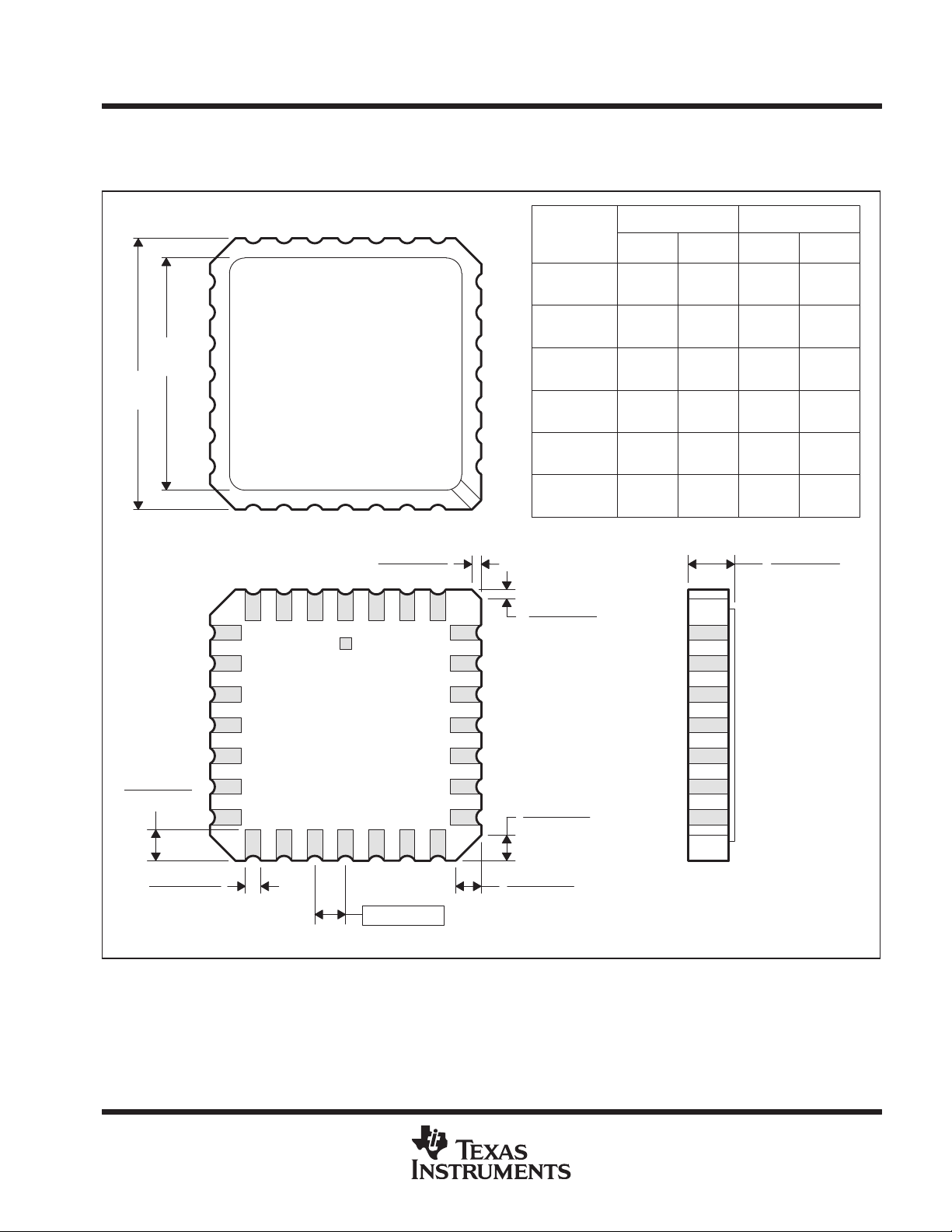
FK (S-CQCC-N**) LEADLESS CERAMIC CHIP CARRIER
28 TERMINAL SHOWN
A SQ
B SQ
19
20
21
22
23
24
25
12826 27
1314151618 17
12
0.020 (0,51)
0.010 (0,25)
MIN
0.342
(8,69)
0.442
0.640
0.740
0.938
1.141
A
(9,09)
(11,63)
(16,76)
(19,32)(18,78)
(24,43)
(29,59)
0.358
0.458
(10,31)
0.660
(12,58)
0.761
(12,58)
0.962
1.165
NO. OF
TERMINALS
**
11
10
9
8
7
6
5
432
20
28
44
52
68
84
0.020 (0,51)
0.010 (0,25)
(11,23)
(16,26)
(23,83)
(28,99)
MINMAX
0.307
(7,80)
0.406
0.495
0.495
0.850
(21,6)
1.047
(26,6)
0.080 (2,03)
0.064 (1,63)
B
MAX
0.358
(9,09)
0.458
(11,63)
0.560
(14,22)
0.560
(14,22)
0.858
(21,8)
1.063
(27,0)
0.055 (1,40)
0.045 (1,14)
0.028 (0,71)
0.022 (0,54)
0.050 (1,27)
NOTES: A. All linear dimensions are in inches (millimeters).
B. This drawing is subject to change without notice.
C. This package can be hermetically sealed with a metal lid.
D. The terminals are gold plated.
E. Falls within JEDEC MS-004
POST OFFICE BOX 655303 • DALLAS, TEXAS 75265
0.045 (1,14)
0.035 (0,89)
0.045 (1,14)
0.035 (0,89)
4040140/C 11/95
15

TLV2352, TLV2352Y
LinCMOS DUAL LOW-VOLTAGE DIFFERENTIAL COMPARATORS
SLCS01 1B – MAY 1992 – REVISED MARCH 1999
MECHANICAL INFORMATION
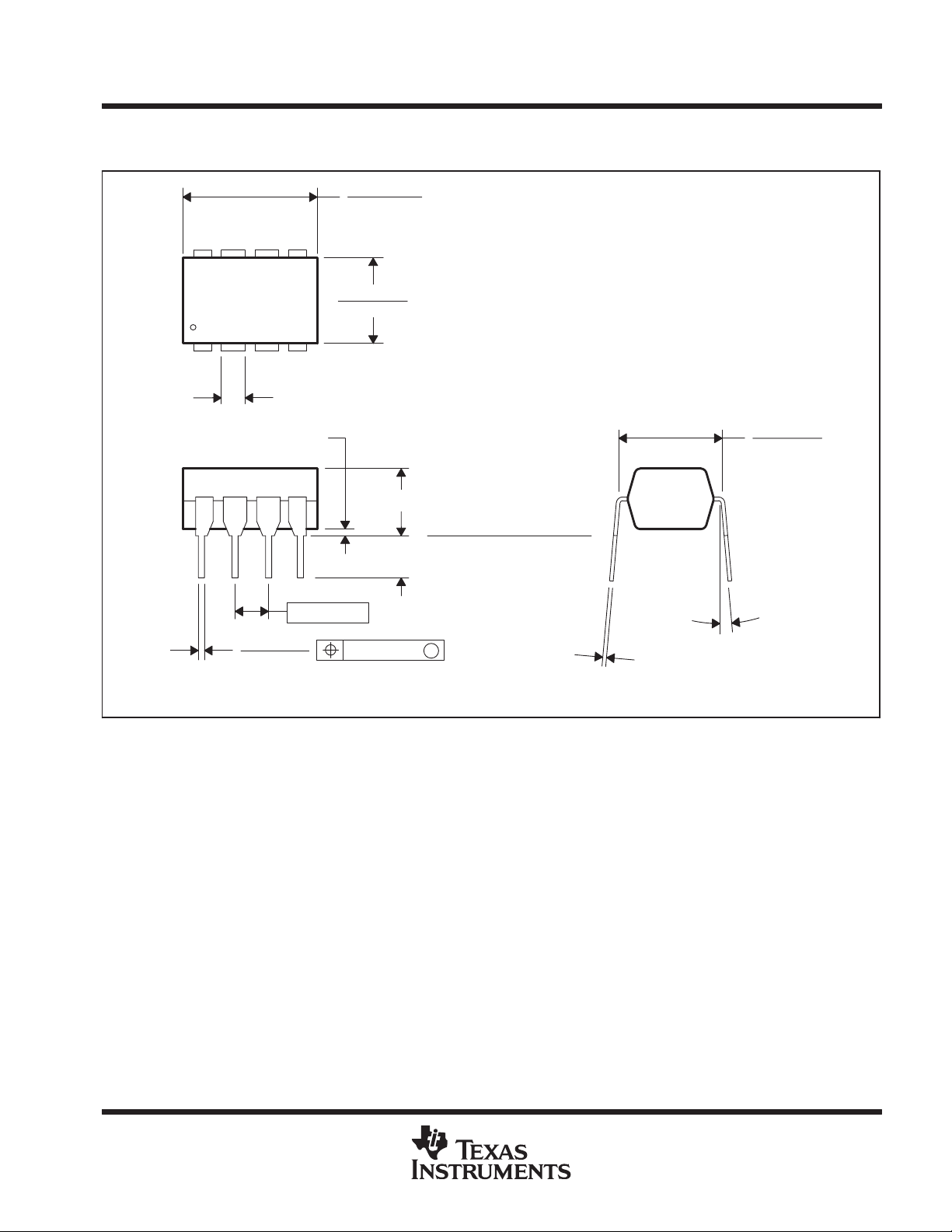
JG (R-GDIP-T8) CERAMIC DUAL-IN-LINE PACKAGE
0.400 (10,20)
0.355 (9,00)
58
0.280 (7,11)
0.245 (6,22)
14
0.065 (1,65)
0.045 (1,14)
0.310 (7,87)
0.020 (0,51) MIN
0.290 (7,37)
0.063 (1,60)
0.015 (0,38)
0.100 (2,54)
NOTES: A. All linear dimensions are in inches (millimeters).
B. This drawing is subject to change without notice.
C. This package can be hermetically sealed with a ceramic lid using glass frit.
D. Index point is provided on cap for terminal identification only on press ceramic glass frit seal only
E. Falls within MIL-STD-1835 GDIP1-T8
0.023 (0,58)
0.015 (0,38)
0.200 (5,08) MAX
Seating Plane
0.130 (3,30) MIN
0°–15°
0.015 (0,38)
0.008 (0,20)
4040107/B 04/95
16
POST OFFICE BOX 655303 • DALLAS, TEXAS 75265
TLV2352, TLV2352Y
LinCMOS DUAL LOW-VOLTAGE DIFFERENTIAL COMPARATORS
SLCS01 1B – MAY 1992 – REVISED MARCH 1999
MECHANICAL INFORMATION
P (R-PDIP-T8) PLASTIC DUAL-IN-LINE PACKAGE
0.400 (10,60)
0.355 (9,02)
58
0.260 (6,60)
0.240 (6,10)
41
0.070 (1,78) MAX
0.020 (0,51) MIN
0.200 (5,08) MAX
0.125 (3,18) MIN
0.100 (2,54)
0.021 (0,53)
0.015 (0,38)
NOTES: A. All linear dimensions are in inches (millimeters).
B. This drawing is subject to change without notice.
C. Falls within JEDEC MS-001
0.010 (0,25)
M
0.310 (7,87)
0.290 (7,37)
Seating Plane
0°–15°
0.010 (0,25) NOM
4040082/B 03/95
POST OFFICE BOX 655303 • DALLAS, TEXAS 75265
17
TLV2352, TLV2352Y
LinCMOS DUAL LOW-VOLTAGE DIFFERENTIAL COMPARATORS
SLCS01 1B – MAY 1992 – REVISED MARCH 1999
MECHANICAL INFORMATION
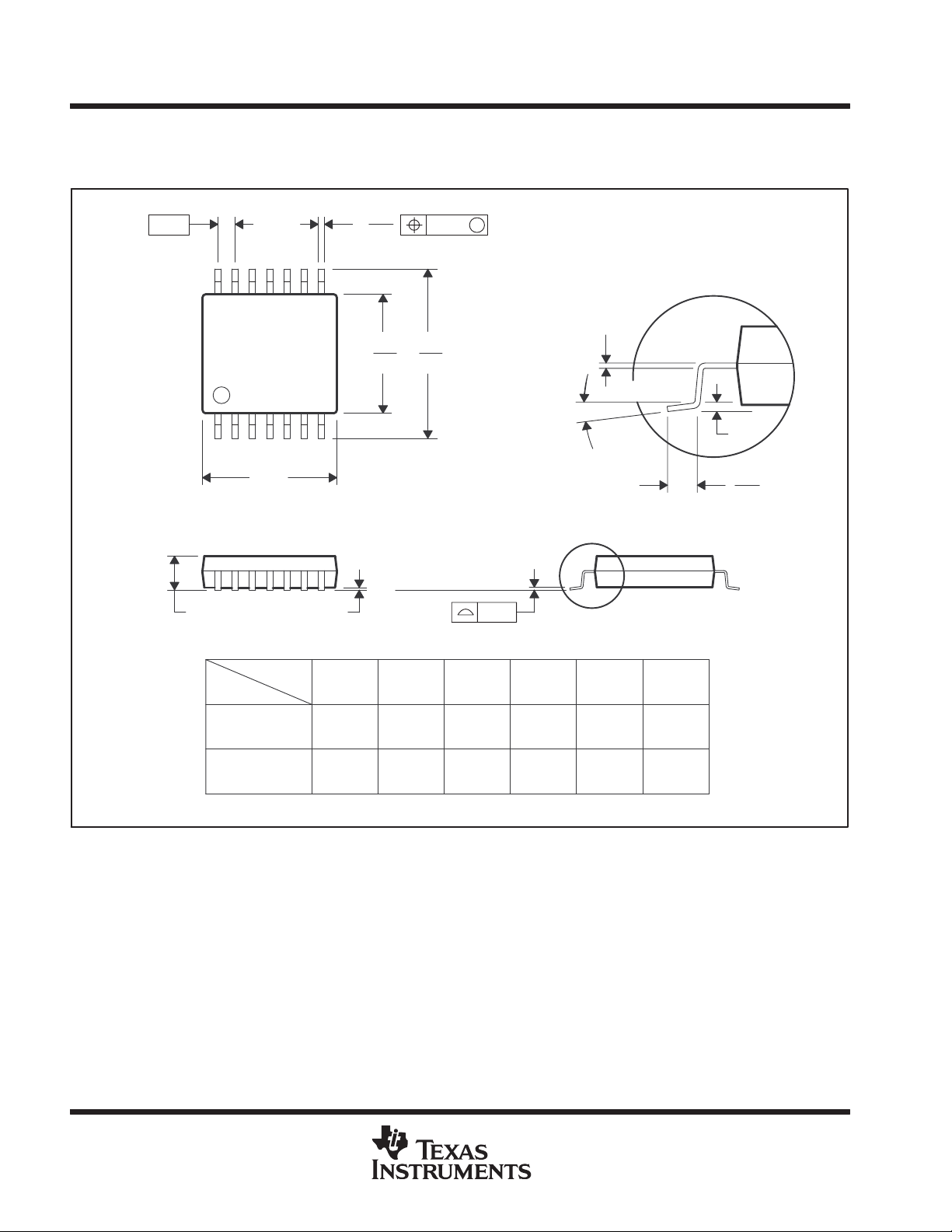
PW (R-PDSO-G**) PLASTIC SMALL-OUTLINE PACKAGE
14 PIN SHOWN
0,65
14
1
1,20 MAX
A
7
0,10 MIN
0,32
0,19
8
6,70
4,50
4,30
6,10
M
0,13
Seating Plane
0,10
0,15 NOM
Gage Plane
0,25
0°–8°
0,75
0,50
PINS **
DIM
A MAX
A MIN
NOTES: A. All linear dimensions are in millimeters.
B. This drawing is subject to change without notice.
C. Body dimensions do not include mold flash or protrusion not to exceed 0,15.
D. Falls within JEDEC MO-153
8
3,10
2,90
14
5,10
4,90
16
5,10
20
6,60
6,404,90
24
7,90
7,70
28
9,80
9,60
4040064/D 10/95
18
POST OFFICE BOX 655303 • DALLAS, TEXAS 75265

TLV2352, TLV2352Y
LinCMOS DUAL LOW-VOLTAGE DIFFERENTIAL COMPARATORS
SLCS01 1B – MAY 1992 – REVISED MARCH 1999
MECHANICAL INFORMATION
U (S-GDFP-F10) CERAMIC DUAL FLATPACK
0.250 (6,35)
0.246 (6,10)
0.006 (0,15)
0.080 (2,03)
0.050 (1,27)
0.004 (0,10)
0.045 (1,14)
0.026 (0,66)
0.250 (6,35)
1
0.250 (6,35)
5
NOTES: A. All linear dimensions are in inches (millimeters).
B. This drawing is subject to change without notice.
C. This package can be hermetically sealed with a ceramic lid using glass frit.
D. Index point is provided on cap for terminal identification only.
E. Falls within MIL STD 1835 GDFP1-F10 and JEDEC MO-092AA
0.300 (7,62)
1.000 (25,40)
0.750 (19,05)
10
0.350 (8,89)0.350 (8,89)
0.250 (6,35)
0.019 (0,48)
0.015 (0,38)
0.050 (1,27)
6
0.025 (0,64)
0.005 (0,13)
4040179/B 03/95
POST OFFICE BOX 655303 • DALLAS, TEXAS 75265
19

IMPORTANT NOTICE
T exas Instruments and its subsidiaries (TI) reserve the right to make changes to their products or to discontinue
any product or service without notice, and advise customers to obtain the latest version of relevant information
to verify, before placing orders, that information being relied on is current and complete. All products are sold
subject to the terms and conditions of sale supplied at the time of order acknowledgement, including those
pertaining to warranty, patent infringement, and limitation of liability.
TI warrants performance of its semiconductor products to the specifications applicable at the time of sale in
accordance with TI’s standard warranty. Testing and other quality control techniques are utilized to the extent
TI deems necessary to support this warranty . Specific testing of all parameters of each device is not necessarily
performed, except those mandated by government requirements.
CERTAIN APPLICATIONS USING SEMICONDUCTOR PRODUCTS MAY INVOLVE POTENTIAL RISKS OF
DEATH, PERSONAL INJURY, OR SEVERE PROPERTY OR ENVIRONMENTAL DAMAGE (“CRITICAL
APPLICATIONS”). TI SEMICONDUCTOR PRODUCTS ARE NOT DESIGNED, AUTHORIZED, OR
WARRANTED TO BE SUITABLE FOR USE IN LIFE-SUPPORT DEVICES OR SYSTEMS OR OTHER
CRITICAL APPLICA TIONS. INCLUSION OF TI PRODUCTS IN SUCH APPLICATIONS IS UNDERST OOD TO
BE FULLY AT THE CUSTOMER’S RISK.
In order to minimize risks associated with the customer’s applications, adequate design and operating
safeguards must be provided by the customer to minimize inherent or procedural hazards.
TI assumes no liability for applications assistance or customer product design. TI does not warrant or represent
that any license, either express or implied, is granted under any patent right, copyright, mask work right, or other
intellectual property right of TI covering or relating to any combination, machine, or process in which such
semiconductor products or services might be or are used. TI’s publication of information regarding any third
party’s products or services does not constitute TI’s approval, warranty or endorsement thereof.
Copyright 1999, Texas Instruments Incorporated
 Loading...