TLC5602C, TLC5602M
VIDEO 8-BIT DIGITAL-TO-ANALOG CONVERTERS
SLAS023C – FEBRUARY 1989 – REVISED MAY 1995
1
POST OFFICE BOX 655303 • DALLAS, TEXAS 75265
D
8-Bit Resolution
D
±0.2% Linearity
D
Maximum Conversion Rate
30 MHz Typ
20 MHz Min
D
Analog Output Voltage Range
V
DD
to VDD –1 V
D
TTL Digital Input Voltage
D
5-V Single Power-Supply Operation
D
Low Power Consumption...80 mW Typ
D
Interchangeable With Fujitsu MB40778
description
The TLC5602x devices are low-power, ultra-high-speed video, digital-to-analog converters that use the
LinEPIC 1-µm CMOS process. The TLC5602x converts digital signals to analog signals at a sampling rate
of dc to 20 MHz. Because of high-speed operation, the TLC5602x devices are suitable for digital video
applications such as digital television, video processing with a computer, and radar-signal processing.
The TLC5602C is characterized for operation from 0°C to 70°C. The TLC5602M is characterized over the full
military temperature range of –55°C to 125°C.
1
2
3
4
5
6
7
8
9
18
17
16
15
14
13
12
11
10
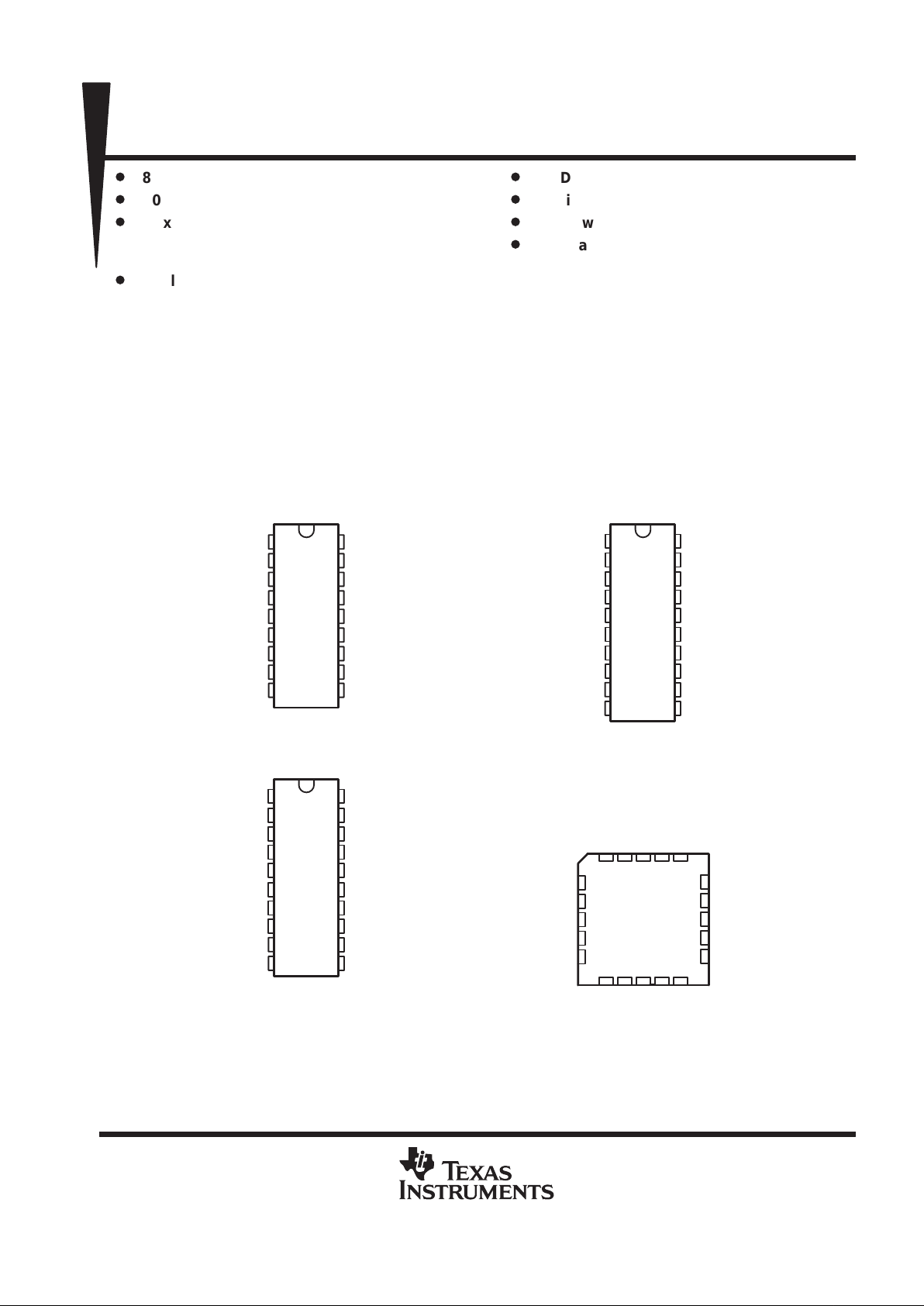
DGTL GND
DGTL V
DD
COMP
REF
ANLG V
DD1
A OUT
ANLG V
DD2
DGTL V
DD
ANLG GND
D0 (LSB)
D1
D2
D3
D4
D5
D6
D7 (MSB)
CLK
N PACKAGE
(TOP VIEW)
1
2
3
4
5
6
7
8
9
10
20
19
18
17
16
15
14
13
12
11
DGTL GND
DGTL V
DD
COMP
REF
ANLG V
DD1
A OUT
NC
ANLG V
DD2
DGTL V
DD
ANLG GND
NC
D0 (LSB)
D1
D2
D3
D4
D5
D6
D7 (MSB)
CLK
NC—No internal connection
DW PACKAGE
(TOP VIEW)
1
2
3
4
5
6
7
8
9
10
20
19
18
17
16
15
14
13
12
11
NC
DGTL GND
DGTL V
DD
COMP
REF
ANLG V
DD1
A OUT
ANLG V
DD2
DGTL V
DD
ANLG GND
NC
D0 (LSB)
D1
D2
D3
D4
D5
D6
D7 (MSB)
CLK
J PACKAGE
(TOP VIEW)
3212019
910111213
4
5
6
7
8
18
17
16
15
14
D1
D2
D3
D4
D5
COMP
REF
ANLG V
DD1
A OUT
ANLG V
DD2
FK PACKAGE
(TOP VIEW)
DGTL V
DGTL GND
NC
D7 (MSB)
D6
NC
D0 (LSB)
ANLG GND
CLK
DD
DGTL V
DD
Copyright 1995, Texas Instruments Incorporated
PRODUCTION DATA information is current as of publication date.
Products conform to specifications per the terms of Texas Instruments
standard warranty. Production processing does not necessarily include
testing of all parameters.
LinEPIC is a trademark of Texas Instruments Incorporated.

TLC5602C, TLC5602M
VIDEO 8-BIT DIGITAL-TO-ANALOG CONVERTERS
SLAS023C – FEBRUARY 1989 – REVISED MAY 1995
2
POST OFFICE BOX 655303 • DALLAS, TEXAS 75265
AVAILABLE OPTIONS
PACKAGE
T
A
WIDE-BODY SMALL OUTLINE
(DW)
CERAMIC CHIP CARRIER
(FK)
CERAMIC DIP
(J)
PLASTIC DIP
(N)
0°C to 70°C TLC5602CDW TLC5602CN
–55°C to 125°C TLC5602MFK TLC5602MJ
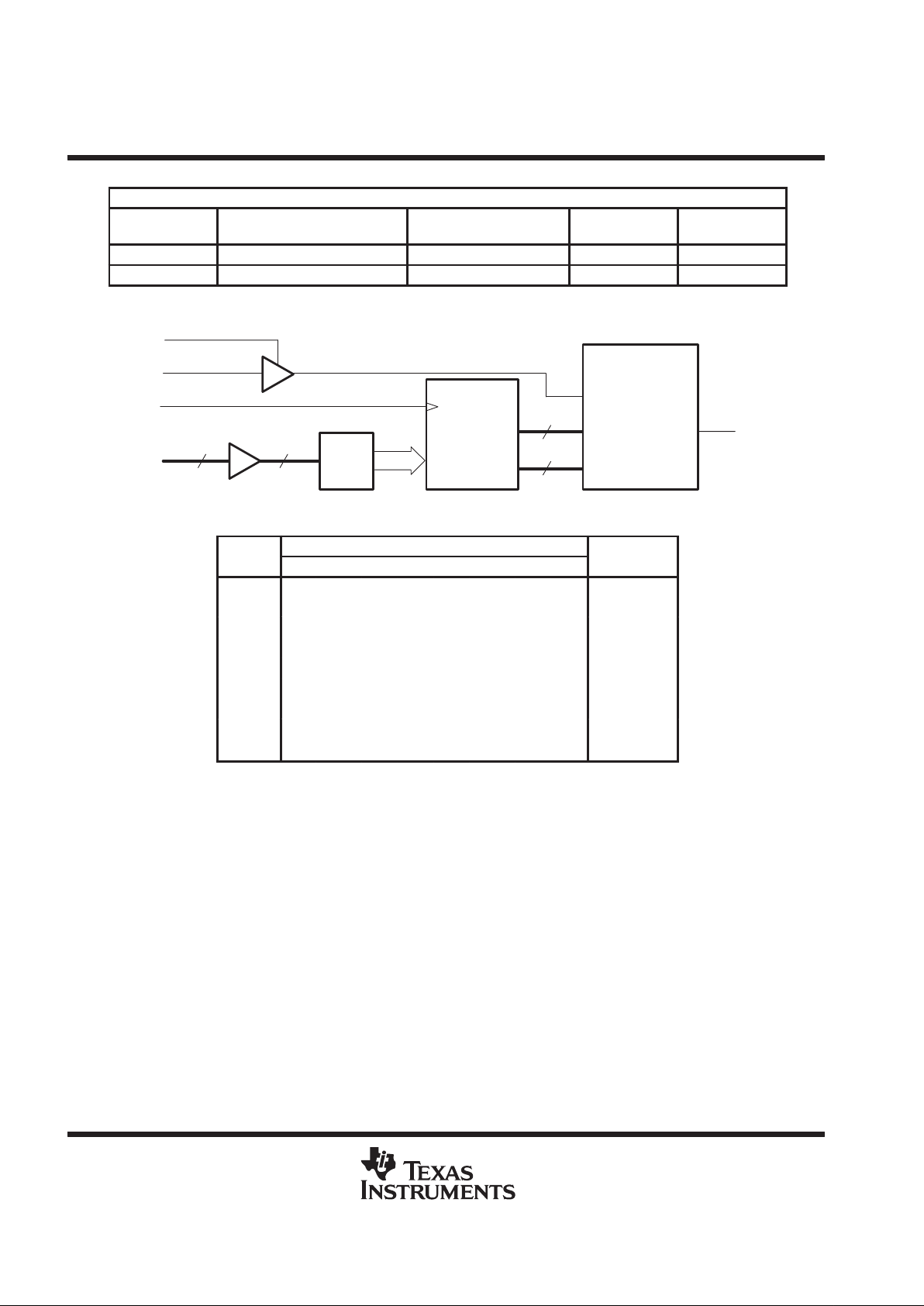
functional block diagram
Buffer
Driver With
Register
Current
Switches
With
Register
Decode
COMP
REF
CLK
D7–D0
A OUT
88
3
63
I x 4
I x 1
FUNCTION TABLE
DIGITAL INPUTS
OUTPUT
STEP
D7 D6 D5 D4 D3 D2 D1 D0
VOLTAGE
†
0 L L L L L L L L 3.980 V
1 L L L L L L L H 3.984 V
| ||
127 L H H H H H H H 4.488 V
128 H L L L L L L L 4.492 V
129 H L L L L L L H 4.496 V
| ||
254 H H H H H H H L 4.996 V
255 H H H H H H H H 5.000 V
†
VDD = 5 V and V
ref
= 4.02 V

TLC5602C, TLC5602M
VIDEO 8-BIT DIGITAL-TO-ANALOG CONVERTERS
SLAS023C – FEBRUARY 1989 – REVISED MAY 1995
3
POST OFFICE BOX 655303 • DALLAS, TEXAS 75265
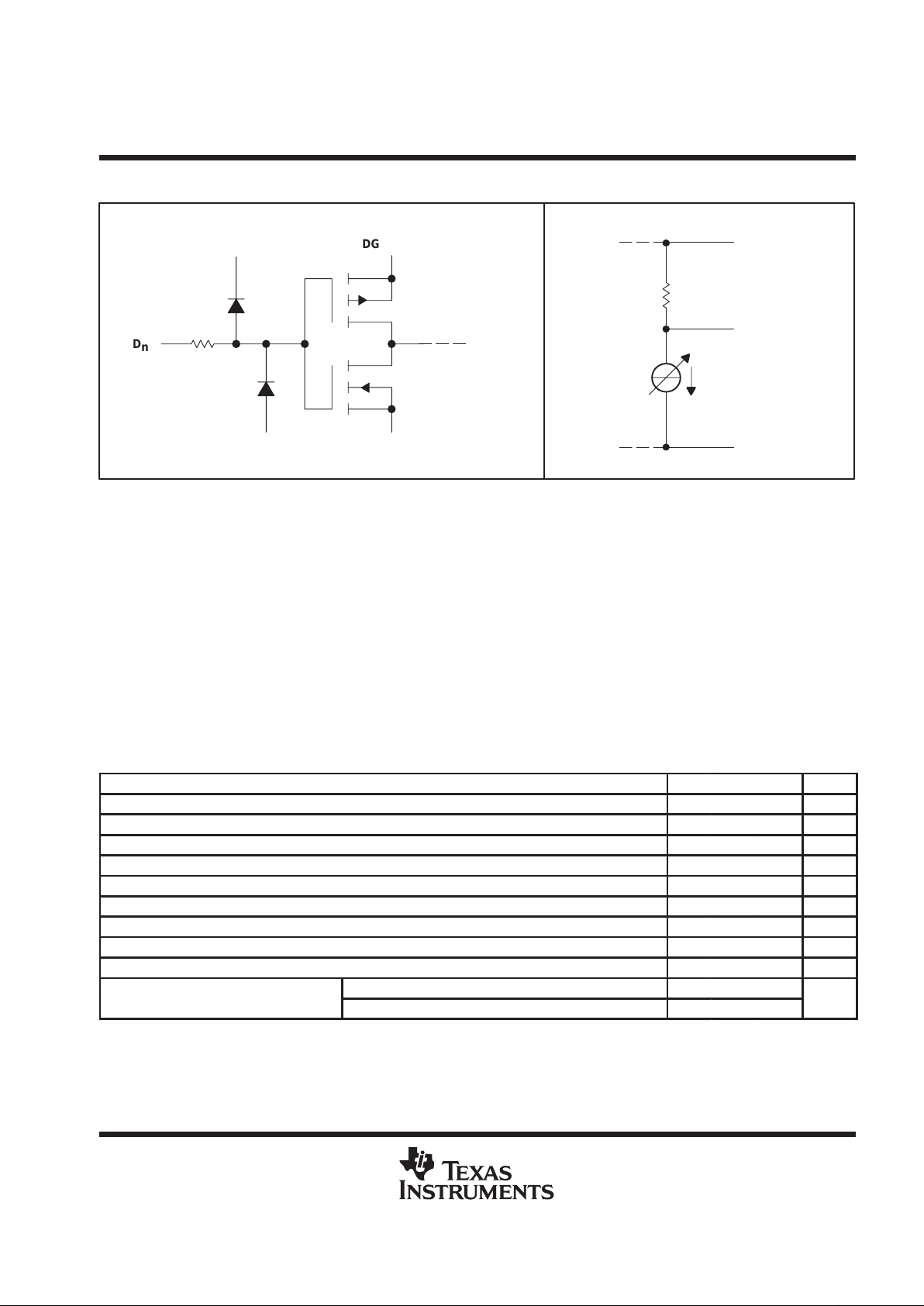
schematics of equivalent input and output
EQUIVALENT OF ANALOG OUTPUTEQUIVALENT OF EACH DIGITAL INPUT
ANLG
‡
GND
A OUT
80 Ω
ANLG V
DD1
D
n
DGTL V
DD
ANLG
‡
GND
DGTL
‡
GND
DGTL V
DD
‡
ANLG GND and DGTL GND do not connect internally and should be tied together as close to the device terminals as possible.
absolute maximum ratings over operating free-air temperature range (unless otherwise noted)
†
Supply voltage range, ANLG V
DD
, DGTL VDD –0.5 V to 7 V. . . . . . . . . . . . . . . . . . . . . . . . . . . . . . . . . . . . . . . . .
Digital input voltage range, V
I
–0.5 V to 7 V. . . . . . . . . . . . . . . . . . . . . . . . . . . . . . . . . . . . . . . . . . . . . . . . . . . . . . . .
Analog reference voltage range, V
ref
V
DD
– 1.7 V to VDD + 0.5 V. . . . . . . . . . . . . . . . . . . . . . . . . . . . . . . . . . .
Operating free-air temperature range, T
A
: TLC5602C 0°C to 70°C. . . . . . . . . . . . . . . . . . . . . . . . . . . . . . . . . . .
TLC5602M –55°C to 125°C. . . . . . . . . . . . . . . . . . . . . . . . . . . . . . .
Storage temperature range, T
stg
–65°C to 150°C. . . . . . . . . . . . . . . . . . . . . . . . . . . . . . . . . . . . . . . . . . . . . . . . . .
Lead temperature 1,6 mm (1/16 inch) from case for 10 seconds 260°C. . . . . . . . . . . . . . . . . . . . . . . . . . . . . . .
†
Stresses beyond those listed under “absolute maximum ratings” may cause permanent damage to the device. These are stress ratings only, and
functional operation of the device at these or any other conditions beyond those indicated under “recommended operating conditions” is not
implied. Exposure to absolute-maximum-rated conditions for extended periods may affect device reliability.
recommended operating conditions
MIN NOM MAX UNIT
Supply voltage, V
DD
4.75 5 5.25 V
Analog reference voltage, V
ref
3.8 4 4.2 V
High-level input voltage, V
IH
2 V
Low-level input voltage, V
IL
0.8 V
Pulse duration, CLK high or low, t
w
25 ns
Setup time, data before CLK↑, t
su
16.5 ns
Hold time, data after CLK↑, t
h
12.5 ns
Phase compensation capacitance, C
comp
(see Note 1) 1 µF
Load resistance, R
L
75k Ω
p
p
TLC5602C 0 70
°
Operating free-air temperature,T
A
TLC5602M –55 125
°C
NOTE 1: The phase compensation capacitor should be connected between COMP and ANLG GND.
 Loading...