

1
2
3
4
5
6
7
14
13
12
11
10
9
8
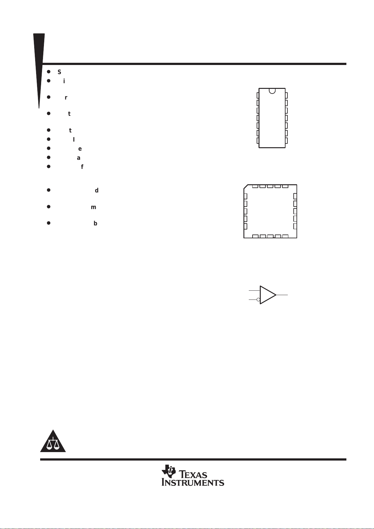
1OUT
2OUT
V
DD
2IN–
2IN+
1IN–
1IN+
3OUT
4OUT
GND
4IN+
4IN–
3IN+
3IN–
D, J, N, OR PW PACKAGE
(TOP VIEW)
3 2 1 20 19
910111213
4
5
6
7
8
18
17
16
15
14
GND
NC
4IN+
NC
4IN–
V
DD
NC
2IN–
NC
2IN+
FK PACKAGE
(TOP VIEW)
2OUT
1OUT
NC
3IN+
4OUT
1IN–
1IN+
NC
NC – No internal connection
3IN–
3OUT
symbol (each comparator)
IN+
IN–
OUT
TLC374, TLC374Q, TLC374Y
LinCMOS QUADRUPLE DIFFERENTIAL COMPARATORS
SLCS118C – NOVEMBER 1983 – REVISED MARCH 1999
1
POST OFFICE BOX 655303 • DALLAS, TEXAS 75265
D
Single- or Dual-Supply Operation
D
Wide Range of Supply Voltages
2 V to 18 V
D
Very Low Supply Current Drain 0.3 mA Typ
at 5 V
D
Fast Response Time . . . 200 ns Typ for
TTL-Level Input Step
D
Built-In ESD Protection
D
High Input Impedance . . . 1012 Ω Typ
D
Extremely Low Input Bias Current 5 pA Typ
D
Ultrastable Low Input Offset Voltage
D
Input Offset Voltage Change at Worst-Case
Input Conditions Typically 0.23 µV/Month,
Including the First 30 Days
D
Common-Mode Input Voltage Range
Includes Ground
D
Outputs Compatible With TTL, MOS, and
CMOS
D
Pin-Compatible With LM339
description
These quadruple differential comparators are
fabricated using LinCMOS technology and
consist of four independent voltage comparators
designed to operate from a single power supply.
Operation from dual supplies is also possible if the
difference between the two supplies is 2 V to 18 V .
Each device features extremely high input
impedance (typically greater than 10
12
Ω),
allowing direct interfacing with high-impedance
sources. The outputs are n-channel open-drain
configurations and can be connected to achieve
positive-logic wired-AND relationships.
The TLC374 has internal electrostatic discharge (ESD) protection circuits and has been classified with a 1000-V
ESD rating using human body model testing. However, care should be exercised in handling this device as
exposure to ESD may result in degradation of the device parametric performance.
The TLC374C is characterized for operation from 0°C to 70°C. The TLC374I is characterized for operation from
–40° to 85°C. The TLC374M is characterized for operation over full military temperature range of
–55°C to 125°C. The TLC374Q is characterized for operation from –40°C to 125°C.
Please be aware that an important notice concerning availability, standard warranty, and use in critical applications of
Texas Instruments semiconductor products and disclaimers thereto appears at the end of this data sheet.
Copyright 1999, Texas Instruments Incorporated
PRODUCTION DATA information is current as of publication date.
Products conform to specifications per the terms of Texas Instruments
standard warranty. Production processing does not necessarily include
testing of all parameters.
LinCMOS is a trademark of Texas Instruments Incorporated.
TLC374, TLC374Q, TLC374Y
LinCMOS QUADRUPLE DIFFERENTIAL COMPARATORS
SLCS118C – NOVEMBER 1983 – REVISED MARCH 1999
2
POST OFFICE BOX 655303 • DALLAS, TEXAS 75265
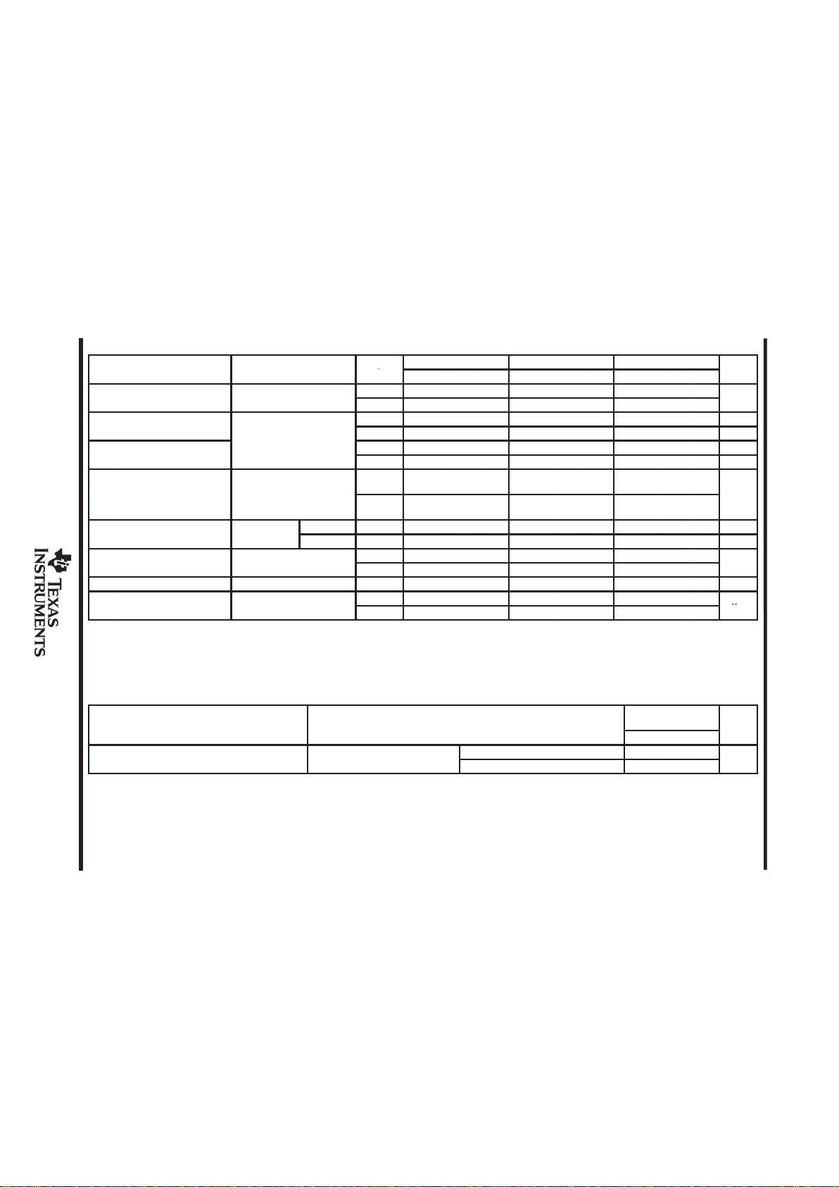
AVAILABLE OPTIONS
PACKAGED DEVICES
CHIP
T
A
V
IO
max
AT 25°C
SMALL OUTLINE
(D)
CHIP CARRIER
(FK)
CERAMIC DIP
(J)
PLASTIC DIP
(N)
TSSOP
(PW)
FORM
(Y)
0°C to 70°C 5 mV TLC374CD — — TLC374CN TLC374CPW TLC374Y
–40°C to 85°C 5 mV TLC374ID — — TLC374IN — —
–55°C to 125°C 5 mV TLC374MD TLC374MFK TLC374MJ TLC374MN — —
–40°C to 125°C 5 mV TLC374QD — — TLC374QN — —
The D packages are available taped and reeled. Add R suffix to device type (e.g., TLC374CDR).
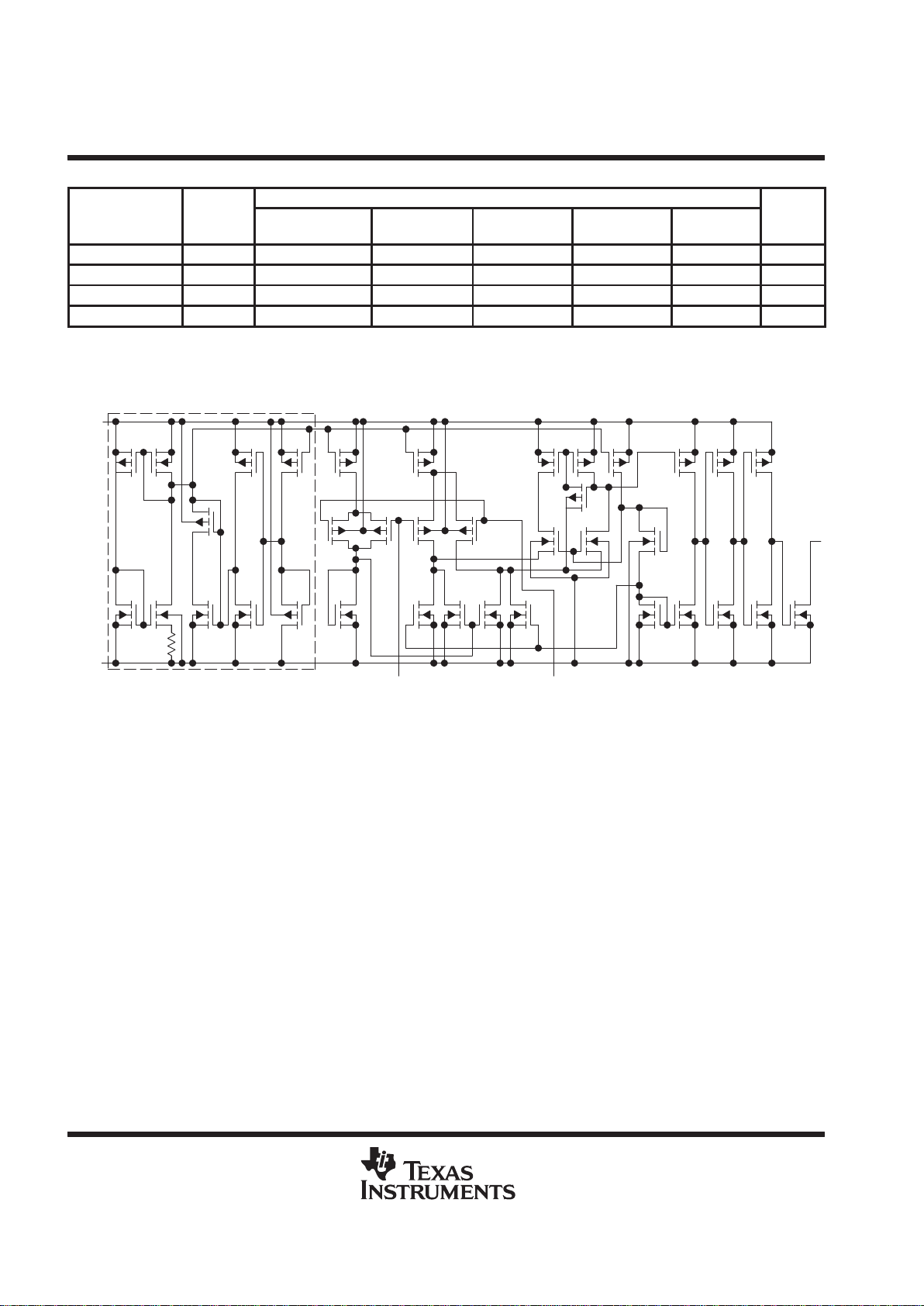
equivalent schematic (each comparator)
V
DD
GND
IN+ IN–
OU
T
Common to All Channels
TLC374, TLC374Q, TLC374Y
LinCMOS QUADRUPLE DIFFERENTIAL COMPARATORS
SLCS118C – NOVEMBER 1983 – REVISED MARCH 1999
3
POST OFFICE BOX 655303 • DALLAS, TEXAS 75265
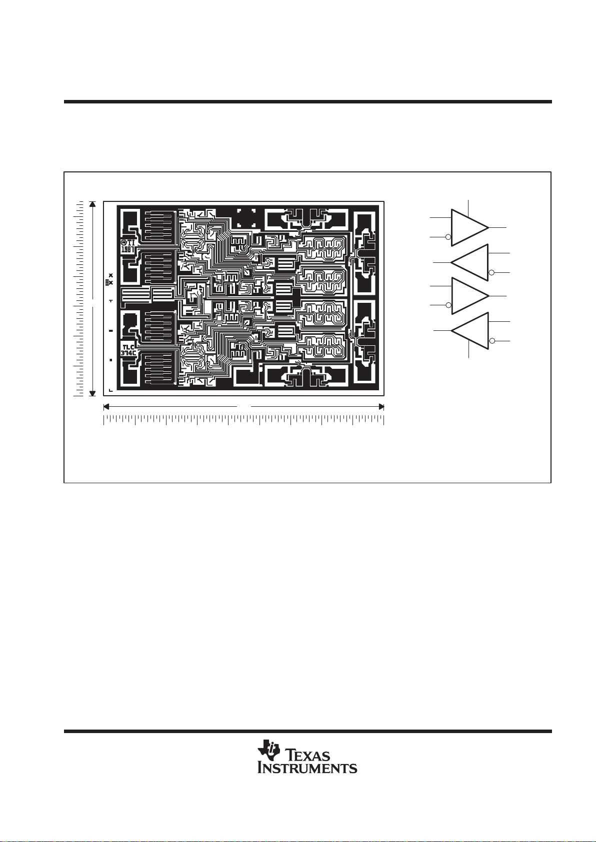
TLC374Y chip information
This chip, when properly assembled, displays characteristics similar to the TLC374C. Thermal compression or
ultrasonic bonding may be used on the doped-aluminum bonding pads. Chips may be mounted with conductive
epoxy or a gold-silicon preform.
BONDING PAD ASSIGNMENTS
CHIP THICKNESS: 15 TYPICAL
BONDING PADS: 4 × 4 MINIMUM
T
JMAX
= 150°C
TOLERANCES ARE ±10%
ALL DIMENSIONS ARE IN MILS.
PIN (4) IS INTERNALLY CONNECTED
TO BACKSIDE OF CHIP.
+
–
3OUT
3IN+
3IN–
GND
(10)
(9)
(8)
(11)
(14)
–
+
(13)
4IN+
4IN–
4OUT
(12)
+
–
V
DD
(3)
(4)
(7)
(6)
(5)
(1)
–
+
(2)
65
90
1IN+
1IN–
2OUT
1OUT
2IN+
2IN–
(13)
(14)
(1)
(2) (3)
(4) (5)
(6)
(7)
(8)
(9)(10)(11)
(12)
TLC374, TLC374Q, TLC374Y
LinCMOS QUADRUPLE DIFFERENTIAL COMPARATORS
SLCS118C – NOVEMBER 1983 – REVISED MARCH 1999
4
POST OFFICE BOX 655303 • DALLAS, TEXAS 75265
absolute maximum ratings over operating free-air temperature range (unless otherwise noted)
†
Supply voltage, V
DD
(see Note 1) 18 V. . . . . . . . . . . . . . . . . . . . . . . . . . . . . . . . . . . . . . . . . . . . . . . . . . . . . . . . . . . .
Differential input voltage, VID (see Note 2) ±18 V. . . . . . . . . . . . . . . . . . . . . . . . . . . . . . . . . . . . . . . . . . . . . . . . . . .
Input voltage, VI V
DD
. . . . . . . . . . . . . . . . . . . . . . . . . . . . . . . . . . . . . . . . . . . . . . . . . . . . . . . . . . . . . . . . . . . . . . . . . . .
Input voltage range, VI –0.3 V to 18 V. . . . . . . . . . . . . . . . . . . . . . . . . . . . . . . . . . . . . . . . . . . . . . . . . . . . . . . . . . . . .
Output voltage, VO 18 V. . . . . . . . . . . . . . . . . . . . . . . . . . . . . . . . . . . . . . . . . . . . . . . . . . . . . . . . . . . . . . . . . . . . . . . . .
Input current, I
I
±5 mA. . . . . . . . . . . . . . . . . . . . . . . . . . . . . . . . . . . . . . . . . . . . . . . . . . . . . . . . . . . . . . . . . . . . . . . . . .
Output current, IO 20 mA. . . . . . . . . . . . . . . . . . . . . . . . . . . . . . . . . . . . . . . . . . . . . . . . . . . . . . . . . . . . . . . . . . . . . . . .
Duration of output short circuit to ground (see Note 3) unlimited. . . . . . . . . . . . . . . . . . . . . . . . . . . . . . . . . . . . . .
Continuous total power dissipation See Dissipation Rating Table. . . . . . . . . . . . . . . . . . . . . . . . . . . . . . . . . . . . .
Operating free-air temperature range, TA: TLC374C 0°C to 70°C. . . . . . . . . . . . . . . . . . . . . . . . . . . . . . . . . . . . .
TLC374I –40°C to 85°C. . . . . . . . . . . . . . . . . . . . . . . . . . . . . . . . . . . .
TLC374M –55°C to 125°C. . . . . . . . . . . . . . . . . . . . . . . . . . . . . . . . . .
TLC374Q –40°C to 125°C. . . . . . . . . . . . . . . . . . . . . . . . . . . . . . . . . .
Storage temperature range, T
stg
–65°C to 150°C. . . . . . . . . . . . . . . . . . . . . . . . . . . . . . . . . . . . . . . . . . . . . . . . . . .
Case temperature range for 60 seconds: FK package 260°C. . . . . . . . . . . . . . . . . . . . . . . . . . . . . . . . . . . . . . . .
Lead temperature 1,6 mm (1/16 inch) from case for 60 seconds: D, N, or PW package 260°C. . . . . . . . . . . .
Lead temperature 1,6 mm (1/16 inch) from case for 10 seconds: J package 300°C. . . . . . . . . . . . . . . . . . . . .
†
Stresses beyond those listed under “absolute maximum ratings” may cause permanent damage to the device. These are stress ratings only, and
functional operation of the device at these or any other conditions beyond those indicated under “recommended operating conditions” is not
implied. Exposure to absolute-maximum-rated conditions for extended periods may affect device reliability.
NOTES: 1. All voltage values except differential voltages are with respect to network ground.
2. Differential voltages are at IN+ with respect to IN –.
3. Short circuits from outputs to VDD can cause excessive heating and eventual device destruction.
DISSIPATION RATING TABLE
T
≤ 25°C DERATING DERATE T
= 70°C T
= 85°C T
= 125°C
PACKAGE
A
POWER RATING FACTOR ABOVE T
A
A
POWER RATINGAPOWER RATINGAPOWER RATING
D 500 mW 7.6 mW/°C 84°C 500 mW 494 mW 190 mW
FK 500 mW 11.0 mW/°C 104°C 500 mW 500 mW 269 mW
J 500 mW 11.0 mW/°C 104°C 500 mW 500 mW 269 mW
N 500 mW 9.2 mW/°C95°C 500 mW 500 mW 224 mW
PW 700 mW 5.6 mW/°C — 448 mW — —
recommended operating conditions
TLC374C TLC374I TLC374M TLC374Q
MIN MAX MIN MAX MIN MAX MIN MAX
UNIT
Supply voltage, V
DD
3 16 3 16 4 16 3 16 V
p
VDD = 5 V 0 3.5 0 3.5 0 3.5 0 3.5
Common-mode input voltage, V
IC
VDD = 10 V 0 8.5 0 8.5 0 8.5 0 8.5
V
Operating free-air temperature, T
A
0 70 –40 85 –55 125 –40 125 °C
TLC374, TLC374Q, TLC374Y
SLCS118C – NOVEMBER 1983 – REVISED MARCH 1999
LinCMOS
QUADRUPLE DIFFERENTIAL COMP ARATORS
POST OFFICE BOX 655303 DALLAS, TEXAS 75265
• 5
electrical characteristics at specified free-air temperature, VDD = 5 V
TLC374C TLC374I TLC374M
PARAMETER
TEST CONDITIONS
T
A
†
MIN TYP MAX MIN TYP MAX MIN TYP MAX
UNIT
p
25°C 1 5 1 5 1 5
VIOInput offset voltage
V
IC
=
V
ICR
min
,
See Note 4
Full range 6.5 7 10
mV
p
25°C 1 1 1 pA
IIOInput offset current
MAX 0.3 1 10 nA
p
25°C 5 5 5 pA
IIBInput bias current
MAX 0.6 2 20 nA
Common-mode input
25°C
0 to
VDD–1
0 to
VDD–1
0 to
VDD–1
V
ICR
voltage range
Full range
0 to
VDD–1.5
0 to
VDD–1.5
0 to
VDD–1.5
V
p
VOH = 5 V 25°C 0.1 0.1 0.1 nA
IOHHigh-level output current
V
ID
= 1
V
VOH = 15 V Full range 1 1 1 µA
p
25°C 150 400 150 400 150 400
VOLLow-level output voltage
V
ID
= –1 V,
I
OL
= 4
mA
Full range 700 700 700
mV
IOLLow-level output current VID = –1 V, VOL = 1.5 V 25°C 6 16 6 16 6 16 mA
Supply current
25°C 300 600 300 600 300 600
I
DD
y
(four comparators)
V
ID
=
1 V
,
No load
Full range 800 800 800
µ
A
†
All characteristics are measured with zero common-mode input voltage unless otherwise noted. Full range is 0°C to 70°C for TLC374C, –40°C to 85°C for TLC374I, and –55°C to
125°C for the TLC374M, and –40°C to 125°C for TLC374Q. MAX is 70°C for TLC374C, 85°C TLC374I, and 125°C for the TLC374M, and 125°C for TLC374Q. IMPORTANT: See
Parameter Measurement Information.
NOTE 4: The offset voltage limits given are the maximum values required to drive the output above 4 V or below 400 mV with a 10-kΩ resistor between the output and VDD. They can
be verified by applying the limit value to the input and checking for the appropriate output state.
switching characteristics, VDD = 5 V, TA = 25°C
PARAMETER TEST CONDITIONS
TLC374C, TLC374I
TLC374M, TLC374Q
UNIT
MIN TYP MAX
p
RL connected to 5 V through 5.1 kΩ,
100-mV input step with 5-mV overdrive 650
Response time
L
g
CL = 15 pF‡, See Note 5
TTL-level input step 200
ns
‡
CL includes probe and jig capacitance.
NOTE 5: The response time specified is the interval between the input step function and the instant when the output crosses 1.4 V.
TLC374, TLC374Q, TLC374Y
LinCMOS QUADRUPLE DIFFERENTIAL COMPARATORS
SLCS118C – NOVEMBER 1983 – REVISED MARCH 1999
6
POST OFFICE BOX 655303 • DALLAS, TEXAS 75265
electrical characteristics at specified free-air temperature, VDD = 5 V , TA = 25°C (unless otherwise
noted)
TLC374Y
PARAMETER
TEST CONDITIONS
MIN TYP MAX
UNIT
V
IO
Input offset voltage VIC = V
ICR
min, See Note 4 1 5 mV
I
IO
Input offset current 1 pA
I
IB
Input bias current 5 pA
V
ICR
Common-mode input voltage range 0 to VDD–1 V
I
OH
High-level output current VID = 1 V, VOH = 5 V 0.1 nA
V
OL
Low-level output voltage VID = –1 V , IOL = 4 mA 150 400 mV
I
OL
Low-level output current VID = –1 V , VOL = 1.5 mV 6 16 mA
I
DD
Supply current (four comparators) VID =1 V, No load 300 600 µA
NOTE 4: The offset voltage limits given are the maximum values required to drive the output above 4 V or below 400 mV with a 10-kΩ resistor
between the output and VDD. They can be verified by applying the limit value to the input and checking for the appropriate output state.
switching characteristics, VDD = 5 V, TA = 25°C
TLC374Y
PARAMETER
TEST CONDITIONS
MIN TYP MAX
UNIT
p
RL connected to 5 V through 5.1 kΩ,
100-mV input step with 5-mV overdrive 650
Response time
L
g
CL = 15 pF†, See Note 5
TTL-level input step 200
ns
†
CL includes probe and jig capacitance.
NOTE 4: The response time specified is the interval between the input step function and the instant when the output crosses 1.4 V.

TLC374, TLC374Q, TLC374Y
LinCMOS QUADRUPLE DIFFERENTIAL COMPARATORS
SLCS118C – NOVEMBER 1983 – REVISED MARCH 1999
7
POST OFFICE BOX 655303 • DALLAS, TEXAS 75265
PARAMETER MEASUREMENT INFORMATION
The digital output stage of the TLC374 can be damaged if it is held in the linear region of the transfer curve.
Conventional operational amplifier/comparator testing incorporates the use of a servo loop that is designed to force
the device output to a level within this linear region. Since the servo-loop method of testing cannot be used, the
following alternative for measuring parameters such as input offset voltage, common-mode rejection, etc., are
offered.
To verify that the input offset voltage falls within the limits specified, the limit value is applied to the input as shown
in Figure 1(a). With the noninverting input positive with respect to the inverting input, the output should be high. With
the input polarity reversed, the output should be low.
A similar test can be made to verify the input offset voltage at the common-mode extremes. The supply voltages can
be slewed as shown in Figure 1(b) for the V
ICR
test, rather than changing the input voltages, to provide greater
accuracy.
A close approximation of the input offset voltage can be obtained by using a binary search method to vary the
differential input voltage while monitoring the output state. When the applied input voltage differential is equal, but
opposite in polarity to the input offset voltage, the output changes state.
5 V
5.1 kΩ
(a) VIO WITH VIC = 0
(b) VIO WITH VIC = 4 V
Applied V
IO
Limit
V
O
1 V
Applied V
IO
Limit
V
O
5.1 kΩ
–4 V
Figure 1. Method for Verifying That Input Offset Voltage is Within Specified Limits
TLC374, TLC374Q, TLC374Y
LinCMOS QUADRUPLE DIFFERENTIAL COMPARATORS
SLCS118C – NOVEMBER 1983 – REVISED MARCH 1999
8
POST OFFICE BOX 655303 • DALLAS, TEXAS 75265
PARAMETER MEASUREMENT INFORMATION
Figure 2 illustrates a practical circuit for direct dc measurement of input offset voltage that does not bias the
comparator into the linear region. The circuit consists of a switching-mode servo loop in which U1a generates a
triangular waveform of approximately 20-mV amplitude. U1b acts as a buffer with C2 and R4 removing any residual
dc offset. The signal is then applied to the inverting input of the comparator under test, while the noninverting input
is driven by the output of the integrator formed by U1c through the voltage divider formed by R9 and R10. The loop
reaches a stable operating point when the output of the comparator under test has a duty cycle of exactly 50%, which
can only occur when the incoming triangle wave is sliced symmetrically or when the voltage at the noninverting input
exactly equals the input offset voltage.
Voltage divider R9 and R10 provide a step up of the input offset voltage by a factor of 100 to make measurement
easier. The values of R5, R8, R9, and R10 can significantly influence the accuracy of the reading; therefore, it is
suggested that their tolerance level be 1% or lower.
Measuring the extremely low values of input current requires isolation from all other sources of leakage current and
compensation for the leakage of the test socket and board. With a good picoammeter, the socket and board leakage
can be measured with no device in the socket. Subsequently , this open-socket leakage value can be subtracted from
the measurement obtained with a device in the socket to obtain the actual input current of the device.
+
–
DUT
+
–
–
+
U1b
1/4 TLC274CN
Buffer
C2
1 µF
R1
240 kΩ
U1a
1/4 TLC274CN
Triangle
Generator
R2
10 kΩ
R3
100 kΩ
C1
0.1 µF
R10
100 Ω, 1%
R9
10 kΩ, 1%
R8
1.8 kΩ, 1%
R7
1 MΩ
R6
5.1 kΩ
R5
1.8 kΩ, 1%
C3
0.68 µF
U1c
1/4 TLC274CN
Integrator
C4
0.1 µF
R4
47 kΩ
V
DD
V
IO
(X100)
Figure 2. Test Circuit for Input Offset Voltage Measurement
TLC374, TLC374Q, TLC374Y
LinCMOS QUADRUPLE DIFFERENTIAL COMPARATORS
SLCS118C – NOVEMBER 1983 – REVISED MARCH 1999
9
POST OFFICE BOX 655303 • DALLAS, TEXAS 75265
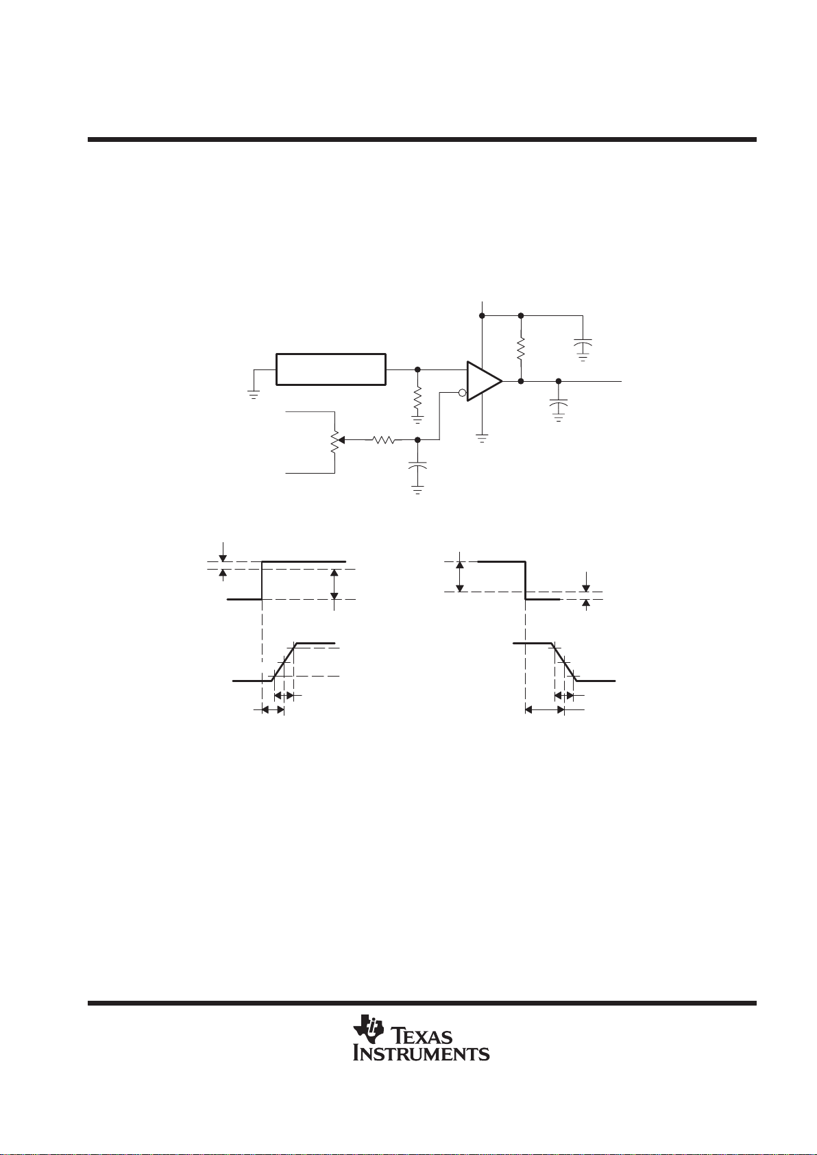
PARAMETER MEASUREMENT INFORMATION
Response time is defined as the interval between the application of an input step function and the instant when the
output reaches 50% of its maximum value. Response time, low-to-high-level output, is measured from the trailing
edge of the input pulse. Response-time measurement at low input signal levels can be greatly affected by the input
offset voltage. The offset voltage should be balanced by the adjustment at the inverting input (as shown in Figure 3)
so that the circuit is just at the transition point. Then a low signal, for example, 105-mV or 5-mV overdrive, causes
the output to change state.
50%
OUT
5.1 kΩ
1 µF
V
DD
Pulse Generator
C
L
(see Note A)
50 Ω
1 kΩ
0.1 µF
TEST CIRCUIT
10 Ω
10 Turn
1 V
–1 V
Input
Offset Voltage
Compensation
Adjustment
VOLTAGE WAVEFORMS
t
PLH
t
r
10%
90%
100 mV
Overdrive
Input
Low-to-HighLevel Output
50%
t
PLH
t
f
10%
90%
100 mV
Overdrive
Input
High-to-LowLevel Output
NOTE A: CL includes probe and jig capacitance.
Figure 3. Response, Rise, and Fall Times Test Circuit and Voltage Waveforms

TLC374, TLC374Q, TLC374Y
LinCMOS QUADRUPLE DIFFERENTIAL COMPARATORS
SLCS118C – NOVEMBER 1983 – REVISED MARCH 1999
10
POST OFFICE BOX 655303 • DALLAS, TEXAS 75265
PRINCIPLES OF OPERATION
LinCMOS process
LinCMOS process is a linear polysilicon-gate complimentary-MOS process. Primarily designed for singlesupply applications, LinCMOS products facilitate the design of a wide range of high-performance analog
functions from operational amplifiers to complex mixed-mode converters.
While digital designers are experienced with CMOS, MOS technologies are relatively new for analog designers.
This short guide is intended to answer the most frequently asked questions related to the quality and reliability
of LinCMOS products. Further questions should be directed to the nearest TI field sales office.
electrostatic discharge
CMOS circuits are prone to gate oxide breakdown when exposed to high voltages even if the exposure is only
for very short periods of time. Electrostatic discharge (ESD) is one of the most common causes of damage to
CMOS devices. It can occur when a device is handled without proper consideration for environmental
electrostatic charges, e.g. during board assembly. If a circuit in which one amplifier from a dual operational
amplifier is being used and the unused pins are left open, high voltages tends to develop. If there is no provision
for ESD protection, these voltages may eventually punch through the gate oxide and cause the device to fail.
To prevent voltage buildup, each pin is protected by internal circuitry.
Standard ESD-protection circuits safely shunt the ESD current by providing a mechanism whereby one or more
transistors break down at voltages higher than normal operating voltages but lower than the breakdown voltage
of the input gate. This type of protection scheme is limited by leakage currents which flow through the shunting
transistors during normal operation after an ESD voltage has occurred. Although these currents are small, on
the order of tens of nanoamps, CMOS amplifiers are often specified to draw input currents as low as tens of
picoamps.
To overcome this limitation, TI design engineers developed the patented ESD-protection circuit shown in
Figure 4. This circuit can withstand several successive 1-kV ESD pulses, while reducing or eliminating leakage
currents that may be drawn through the input pins. A more detailed discussion of the operation of TI’s
ESD-protection circuit is presented on the next page.
All input an output pins of LinCMOS and Advanced LinCMOS products have associated ESD-protection
circuitry that undergoes qualification testing to withstand 1000 V discharged from a 100-pF capacitor through
a 1500-Ω resistor (human body model) and 200 V from a 100-pF capacitor with no current-limiting resistor
(charged device model). These tests simulate both operator and machine handling of devices during normal
test and assembly operations.
D1 D2
Q2
R2
D3
Q1
R1
V
DD
To Protected CircuitInput
V
SS
Figure 4. LinCMOS ESD-Protection Schematic

TLC374, TLC374Q, TLC374Y
LinCMOS QUADRUPLE DIFFERENTIAL COMPARATORS
SLCS118C – NOVEMBER 1983 – REVISED MARCH 1999
11
POST OFFICE BOX 655303 • DALLAS, TEXAS 75265
PRINCIPLES OF OPERATION
Input protection circuit operation
Texas Instruments patented protection circuitry allows for both positive- and negative-going ESD transients.
These transients are characterized by extremely fast rise times and usually low energies, and can occur both
when the device has all pins open and when it is installed in a circuit.
positive ESD transients
Initial positive charged energy is shunted through Q1 to VSS. Q1 turns on when the voltage at the input rises
above the voltage on V
DD
by a value equal to the VEB of Q1. The base current increases through R2 with input
current as Q1 saturates. The base current through R2 as Q1 saturates forces the voltage at the drain and gate
of Q2 to exceed its threshold level (V
T
∼ 22 to 26 V) and turn on Q2. The shunted input current through Q1 to
VSS is now shunted through the n-channel enhancement-type MOSFET Q2 to VSS. If the voltage on the input
pin continues to rise, the breakdown voltage of d3 is exceeded and all remaining energy is dissipated in R1 and
D3. The breakdown voltage of D3 is designed to be 24 V to 27 V , which is well below the gate oxide voltage of
the circuit to be protected.
negative ESD transients
The negative charged ESD transients are shunted directly through D1. Additional energy is dissipated in R1
and D2 as D2 becomes forward-biased. The voltage seen by the protected circuit is –0.3 V to –1 V (the forward
voltage of D1 and D2).
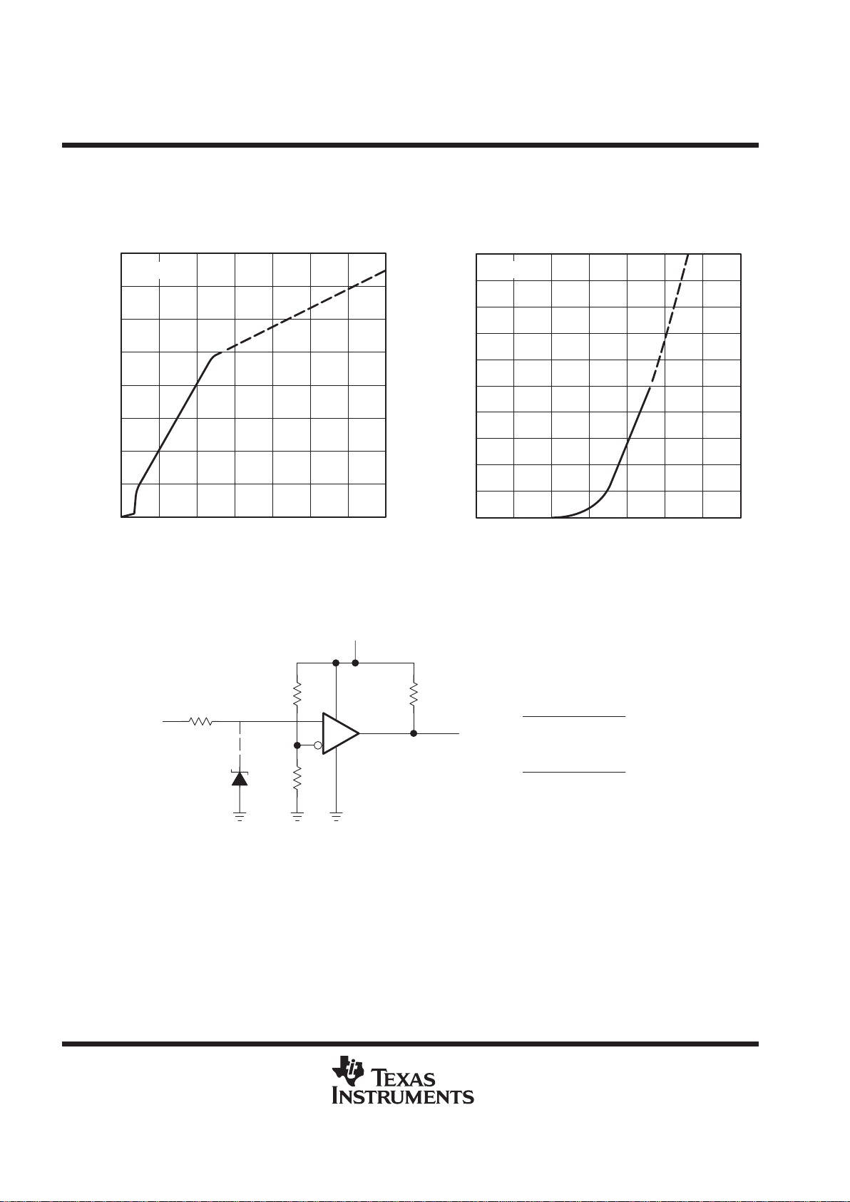
circuit-design considerations
LinCMOS products are being used in actual circuits environments that have input voltages that exceed the
recommended common-mode input voltage range and activate the input protection circuit. Even under normal
operation, these conditions occur during circuit power up or power down, and in many cases, when the device
is being used for a signal conditioning function. The input voltages can exceed V
ICR
and not damage the device
only if the inputs are current limited. The recommended current limit shown on most product data sheets is
±5 mA. Figures 5 and 6 show typical characteristics for input voltage vs input current.
Normal operation and correct output state can be expected even when the input voltage exceeds the positive
supply voltage. The input current should be externally limited even through internal positive current limiting is
achieved in the input protection circuit by the action of Q1. When Q1 is on, it saturates and limits the current
to approximately 5-mA collector current by design. When saturated, Q1 base current increases with input
current. This current is forced into the V
DD
pin and into the device IDD or the VDD supply through R2 producing
the current limiting effects shown in Figure 5. This internal limiting lasts only as long as the input voltage is below
the V
T
of Q2.
When the input voltage exceeds the negative supply voltage, normal operation is affected and output voltage
states may not be correct. Also, the isolation between channels of multiple devices (duals and quads) can be
severely affected. External current limiting must be used since this current is directly shunted by D1 and D2,
and no internal limiting is achieved. If normal output voltage states are required, an external input voltage clamp
is required (see Figure 7).
TLC374, TLC374Q, TLC374Y
LinCMOS QUADRUPLE DIFFERENTIAL COMPARATORS
SLCS118C – NOVEMBER 1983 – REVISED MARCH 1999
12
POST OFFICE BOX 655303 • DALLAS, TEXAS 75265
PRINCIPLES OF OPERATION
Figure 5
3
2
1
0
4
5
6
7
8
II – Input Current – mA
I
I
INPUT CURRENT
vs
INPUT VOLTAGE
†
VI – Input Voltage – V
V
DD
VDD +4 VDD +8 VDD +12
TA = 25°C
†
The dashed line identifies an area of operation where some
degradation of parametric performance may be experienced.
Figure 6
3
2
1
0
4
5
6
7
8
II – Input Current – mA
I
I
INPUT CURRENT
vs
INPUT VOLTAGE
†
VI – Input Voltage – V
VDD– 0.3 VDD – 0.5 VDD – 0.7 VDD – 0.9
TA = 25°C
9
10
†
The dashed line identifies an area of operation where some
degradation of parametric performance may be experienced.
See Note A
5 mA
+
–
R
L
V
DD
1/4
TLC374
R
L
V
REF
V
I
+VI – VDD – 0.3 V
RI =
Positive Voltage Input Current Limit:
5 mA
–VI – VDD – (0.3 V)
RI =
Negative Voltage Input Current Limit:
NOTE A: If the correct output state is required when the negative input exceeds VSS, a Schotty clamp is required.
Figure 7. Typical Input Current-Limiting Configuration for a LinCMOS Comparator
TLC374, TLC374Q, TLC374Y
LinCMOS QUADRUPLE DIFFERENTIAL COMPARATORS
SLCS118C – NOVEMBER 1983 – REVISED MARCH 1999
13
POST OFFICE BOX 655303 • DALLAS, TEXAS 75265
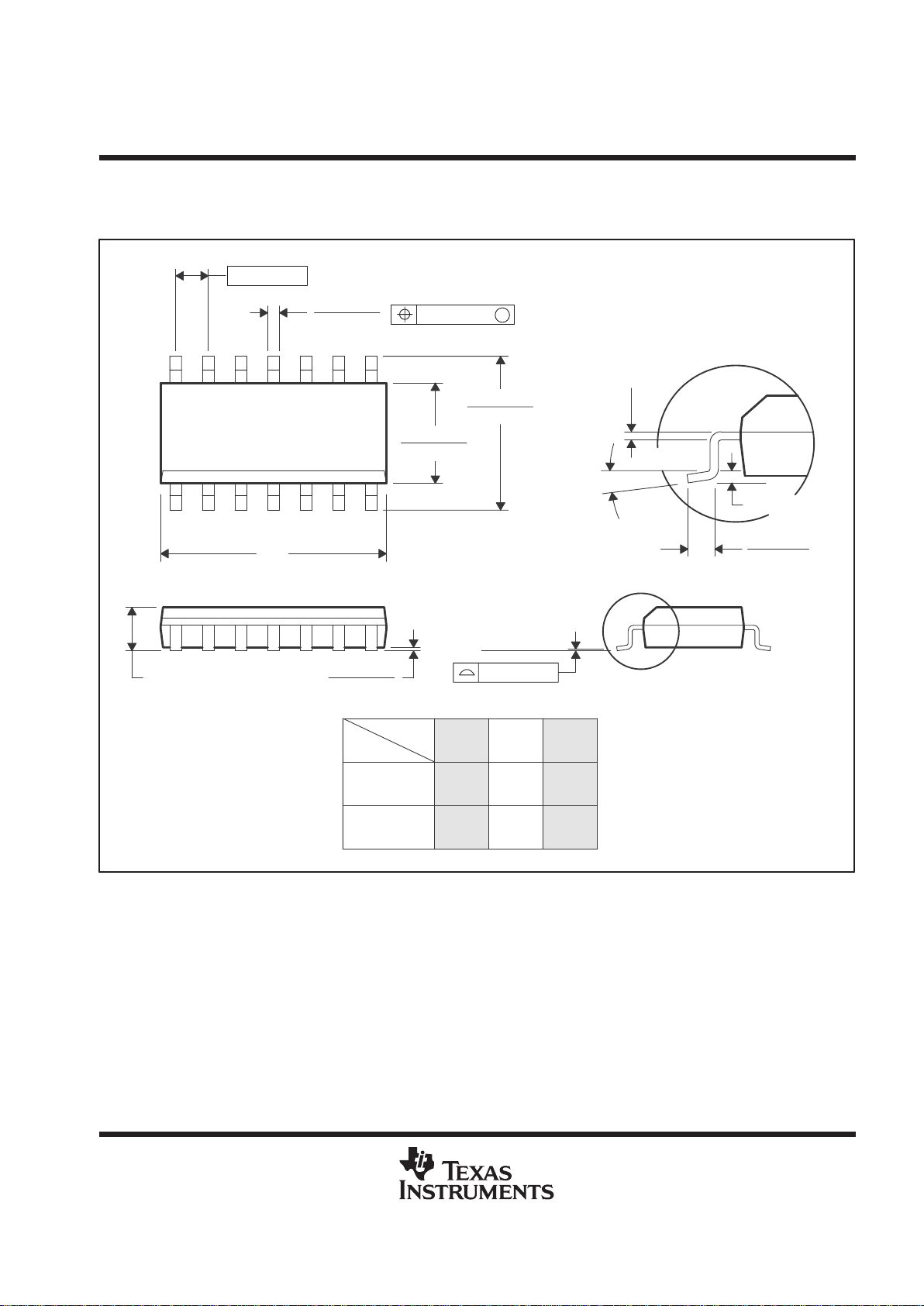
MECHANICAL INFORMATION
D (R-PDSO-G**) PLASTIC SMALL-OUTLINE PACKAGE
14 PIN SHOWN
4040047/D 10/96
0.228 (5,80)
0.244 (6,20)
0.069 (1,75) MAX
0.010 (0,25)
0.004 (0,10)
1
14
0.014 (0,35)
0.020 (0,51)
A
0.157 (4,00)
0.150 (3,81)
7
8
0.044 (1,12)
0.016 (0,40)
Seating Plane
0.010 (0,25)
PINS **
0.008 (0,20) NOM
A MIN
A MAX
DIM
Gage Plane
0.189
(4,80)
(5,00)
0.197
8
(8,55)
(8,75)
0.337
14
0.344
(9,80)
16
0.394
(10,00)
0.386
0.004 (0,10)
M
0.010 (0,25)
0.050 (1,27)
0°–8°
NOTES: A. All linear dimensions are in inches (millimeters).
B. This drawing is subject to change without notice.
C. Body dimensions do not include mold flash or protrusion, not to exceed 0.006 (0,15).
D. Falls within JEDEC MS-012

TLC374, TLC374Q, TLC374Y
LinCMOS QUADRUPLE DIFFERENTIAL COMPARATORS
SLCS118C – NOVEMBER 1983 – REVISED MARCH 1999
14
POST OFFICE BOX 655303 • DALLAS, TEXAS 75265
MECHANICAL INFORMATION
FK (S-CQCC-N**) LEADLESS CERAMIC CHIP CARRIER
4040140/D 10/96
28 TERMINAL SHOWN
B
0.358
(9,09)
MAX
(11,63)
0.560
(14,22)
0.560
0.458
0.858
(21,8)
1.063
(27,0)
(14,22)
A
NO. OF
MINMAX
0.358
0.660
0.761
0.458
0.342
(8,69)
MIN
(11,23)
(16,26)
0.640
0.739
0.442
(9,09)
(11,63)
(16,76)
0.962
1.165
(23,83)
0.938
(28,99)
1.141
(24,43)
(29,59)
(19,32)(18,78)
**
20
28
52
44
68
84
0.020 (0,51)
TERMINALS
0.080 (2,03)
0.064 (1,63)
(7,80)
0.307
(10,31)
0.406
(12,58)
0.495
(12,58)
0.495
(21,6)
0.850
(26,6)
1.047
0.045 (1,14)
0.045 (1,14)
0.035 (0,89)
0.035 (0,89)
0.010 (0,25)
12
1314151618 17
11
10
8
9
7
5
432
0.020 (0,51)
0.010 (0,25)
6
12826 27
19
21
B SQ
A SQ
22
23
24
25
20
0.055 (1,40)
0.045 (1,14)
0.028 (0,71)
0.022 (0,54)
0.050 (1,27)
NOTES: A. All linear dimensions are in inches (millimeters).
B. This drawing is subject to change without notice.
C. This package can be hermetically sealed with a metal lid.
D. The terminals are gold plated.
E. Falls within JEDEC MS-004

TLC374, TLC374Q, TLC374Y
LinCMOS QUADRUPLE DIFFERENTIAL COMPARATORS
SLCS118C – NOVEMBER 1983 – REVISED MARCH 1999
15
POST OFFICE BOX 655303 • DALLAS, TEXAS 75265
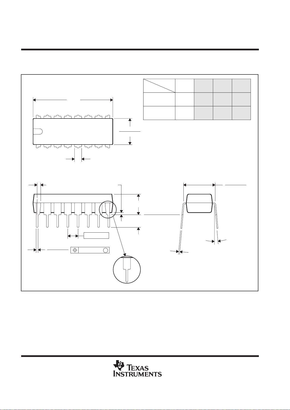
MECHANICAL INFORMATION
J (R-GDIP-T**) CERAMIC DUAL-IN-LINE PACKAGE
14 PIN SHOWN
20
0.290
(7,87)
0.310
0.975
(24,77)
(23,62)
0.930
(7,37)
0.245
(6,22)
(7,62)
0.300
181614
PINS **
0.290
(7,87)
0.310
0.785
(19,94)
(19,18)
0.755
(7,37)
0.310
(7,87)
(7,37)
0.290
0.755
(19,18)
(19,94)
0.785
0.245
(6,22)
(7,11)
0.280A0.300
(7,62)
(6,22)
0.245
A MIN
A MAX
B MAX
B MIN
C MIN
C MAX
DIM
0.310
(7,87)
(7,37)
0.290
(23,10)
0.910
0.300
(7,62)
(6,22)
0.245
Seating Plane
0.014 (0,36)
0.008 (0,20)
4040083/C 08/96
C
8
7
0.020 (0,51) MIN
B
0.070 (1,78)
0.100 (2,54)
0.065 (1,65)
0.045 (1,14)
14
1
0.015 (0,38)
0.023 (0,58)
0.200 (5,08) MAX
0.130 (3,30) MIN
0.100 (2,54)
0°–15°
NOTES: A. All linear dimensions are in inches (millimeters).
B. This drawing is subject to change without notice.
C. This package can be hermetically sealed with a ceramic lid using glass frit.
D. Index point is provided on cap for terminal identification only on press ceramic glass frit seal only.
E. Falls within MIL-STD-1835 GDIP1-T14, GDIP1-T16, GDIP1-T18, and GDIP1-T20
TLC374, TLC374Q, TLC374Y
LinCMOS QUADRUPLE DIFFERENTIAL COMPARATORS
SLCS118C – NOVEMBER 1983 – REVISED MARCH 1999
16
POST OFFICE BOX 655303 • DALLAS, TEXAS 75265
MECHANICAL INFORMATION
N (R-PDIP-T**) PLASTIC DUAL-IN-LINE PACKAGE
20
0.975
(24,77)
0.940
(23,88)
18
0.920
0.850
14
0.775
0.745
(19,69)
(18,92)
16
0.775
(19,69)
(18,92)
0.745
A MIN
DIM
A MAX
PINS **
0.310 (7,87)
0.290 (7,37)
(23.37)
(21.59)
Seating Plane
0.010 (0,25) NOM
14/18 PIN ONL Y
4040049/C 08/95
9
8
0.070 (1,78) MAX
A
0.035 (0,89) MAX
0.020 (0,51) MIN
16
1
0.015 (0,38)
0.021 (0,53)
0.200 (5,08) MAX
0.125 (3,18) MIN
0.240 (6,10)
0.260 (6,60)
M
0.010 (0,25)
0.100 (2,54)
0°–15°
16 PIN SHOWN
NOTES: A. All linear dimensions are in inches (millimeters).
B. This drawing is subject to change without notice.
C. Falls within JEDEC MS-001 (20 pin package is shorter then MS-001.)

TLC374, TLC374Q, TLC374Y
LinCMOS QUADRUPLE DIFFERENTIAL COMPARATORS
SLCS118C – NOVEMBER 1983 – REVISED MARCH 1999
17
POST OFFICE BOX 655303 • DALLAS, TEXAS 75265
MECHANICAL INFORMATION
PW (R-PDSO-G**) PLASTIC SMALL-OUTLINE PACKAGE
4040064/E 08/96
14 PIN SHOWN
Seating Plane
0,05 MIN
1,20 MAX
1
A
7
14
0,19
4,50
4,30
8
6,20
6,60
0,30
0,75
0,50
0,25
Gage Plane
0,15 NOM
0,65
M
0,10
0°–8°
0,10
PINS **
A MIN
A MAX
DIM
2,90
3,10
8
4,90
5,10
14
6,60
6,404,90
5,10
16
7,70
20
7,90
24
9,60
9,80
28
NOTES: A. All linear dimensions are in millimeters.
B. This drawing is subject to change without notice.
C. Body dimensions do not include mold flash or protrusion not to exceed 0,15.
D. Falls within JEDEC MO-153

IMPORTANT NOTICE
T exas Instruments and its subsidiaries (TI) reserve the right to make changes to their products or to discontinue
any product or service without notice, and advise customers to obtain the latest version of relevant information
to verify, before placing orders, that information being relied on is current and complete. All products are sold
subject to the terms and conditions of sale supplied at the time of order acknowledgement, including those
pertaining to warranty, patent infringement, and limitation of liability.
TI warrants performance of its semiconductor products to the specifications applicable at the time of sale in
accordance with TI’s standard warranty. Testing and other quality control techniques are utilized to the extent
TI deems necessary to support this warranty. Specific testing of all parameters of each device is not necessarily
performed, except those mandated by government requirements.
CERT AIN APPLICATIONS USING SEMICONDUCTOR PRODUCTS MAY INVOLVE POTENTIAL RISKS OF
DEATH, PERSONAL INJURY, OR SEVERE PROPERTY OR ENVIRONMENTAL DAMAGE (“CRITICAL
APPLICATIONS”). TI SEMICONDUCTOR PRODUCTS ARE NOT DESIGNED, AUTHORIZED, OR
WARRANTED TO BE SUITABLE FOR USE IN LIFE-SUPPORT DEVICES OR SYSTEMS OR OTHER
CRITICAL APPLICATIONS. INCLUSION OF TI PRODUCTS IN SUCH APPLICA TIONS IS UNDERSTOOD T O
BE FULLY AT THE CUSTOMER’S RISK.
In order to minimize risks associated with the customer’s applications, adequate design and operating
safeguards must be provided by the customer to minimize inherent or procedural hazards.
TI assumes no liability for applications assistance or customer product design. TI does not warrant or represent
that any license, either express or implied, is granted under any patent right, copyright, mask work right, or other
intellectual property right of TI covering or relating to any combination, machine, or process in which such
semiconductor products or services might be or are used. TI’s publication of information regarding any third
party’s products or services does not constitute TI’s approval, warranty or endorsement thereof.
Copyright 1999, Texas Instruments Incorporated
 Loading...