

Page 1
查询TLC3544CDWR供应商
5-V ANALOG, 3-/5-V DIGITAL, 14-BIT, 200-KSPS, 4-/8-CHANNELS SERIAL
ANALOG-TO-DIGITAL CONVERTERS WITH 0-5 V (PSEUDODIFFERENTIAL) INPUTS
TLC3544, TLC3548
SLAS266C – OCTOBER 2000 – REVISED MA Y 2003
D 14-Bit Resolution
D Maximum Throughput 200 KSPS
D Analog Input Range 0-V to Reference
Voltage
D Multiple Analog Inputs:
– 8 Channels for TLC3548
– 4 Channels for TLC3544
D Pseudodifferential Analog Inputs
D SPI/DSP-Compatible Serial Interfaces With
SCLK up to 25 MHz
D Single 5-V Analog Supply; 3-/5-V Digital
Supply
D Low Power:
– 4 mA (Internal Reference: 1.8 mA) for
Normal Operation
– 20 µA in Autopower-Down
D Built-In 4-V Reference, Conversion Clock
and 8x FIFO
D Hardware-Controlled and Programmable
Sampling Period
D Programmable Autochannel Sweep and
Repeat
D Hardware Default Configuration
D INL: ±1 LSB Max
D DNL: ±1 LSB Max
D SINAD: 80.8 dB
D THD: –95 dB
description
SCLK
FS
SDI
EOC/INT
SDO
DGND
DV
DD
CS
A0
A1
A2
A3
SCLK
FS
SDI
EOC/INT
SDO
DGND
DV
DD
CS
A0
A1
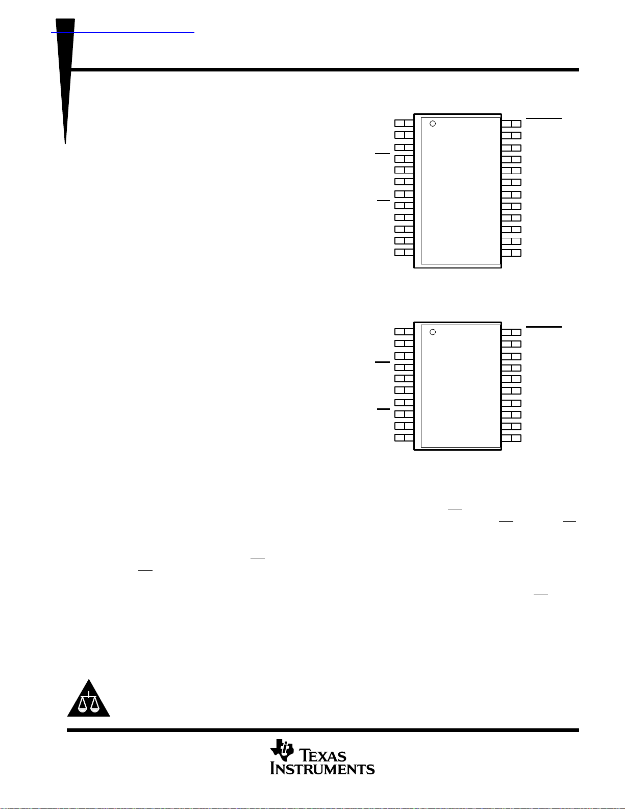
TLC3548
DW OR PW PACKAGE
(TOP VIEW)
1
2
3
4
5
6
7
8
9
10
11
12
TLC3544
DW OR PW PACKAGE
(TOP VIEW)
1
2
3
4
5
6
7
8
9
10
24
23
22
21
20
19
18
17
16
15
14
13
20
19
18
17
16
15
14
13
12
11
CSTART
AV
DD
AGND
BGAP
REFM
REFP
AGND
AV
DD
A7
A6
A5
A4
CSTART
AV
DD
AGND
BGAP
REFM
REFP
AGND
AV
DD
A3
A2
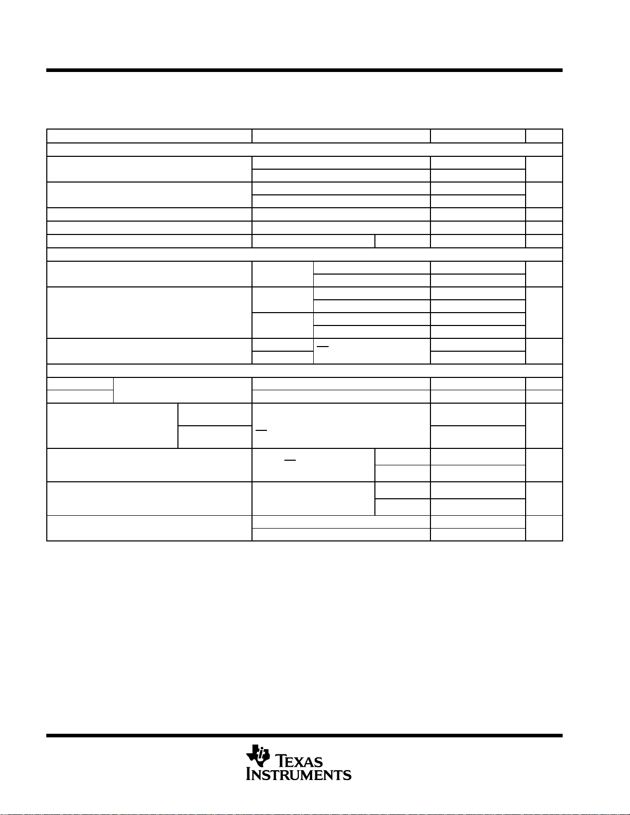
The TLC3544 and TLC3548 are a family of 14-bit resolution high-performance, low-power, CMOS
analog-to-digital converters (ADC). All devices operate from a single 5-V analog power supply and 3-V to 5-V
digital supply. The serial interface consists of four digital inputs [chip select (CS
input-output clock (SCLK), serial data input (SDI)], and a 3-state serial data output (SDO). CS
), frame sync (FS), serial
(works as SS,
slave select), SDI, SDO, and SCLK form an SPI interface. FS, SDI, SDO, and SCLK form a DSP interface. The
frame sync signal (FS) indicates the start of a serial data frame being transferred. When multiple converters
connect to one serial port of a DSP, CS
converter. CS
can be tied to ground if only one converter is used. FS must be tied to DVDD if it is not used (such
as in an SPI interface). When SDI is tied to DV
works as the chip select to allow the host DSP to access the individual
, the device is set in hardware default mode after power-on,
DD
and no software configuration is required. In the simplest case, only three wires (SDO, SCLK, and CS
are needed to interface with the host.
Please be aware that an important notice concerning availability, standard warranty, and use in critical applications of
Texas Instruments semiconductor products and disclaimers thereto appears at the end of this data sheet.
PRODUCTION DATA information is current as of publication date.
Products conform to specifications per the terms of Texas Instruments
standard warranty. Production processing does not necessarily include
testing of all parameters.
POST OFFICE BOX 655303 • DALLAS, TEXAS 75265
Copyright 2000 – 2003, Texas Instruments Incorporated
or FS)
1
Page 2
TLC3544, TLC3548
5-V ANALOG, 3-/5-V DIGITAL, 14-BIT, 200-KSPS, 4-/8-CHANNELS SERIAL
ANALOG-TO-DIGITAL CONVERTERS WITH 0-5 V (PSEUDODIFFERENTIAL) INPUTS
SLAS266C – OCTOBER 2000 – REVISED MAY 2003
description (continued)
In addition to being a high-speed ADC with versatile control capability , these devices have an on-chip analog
multiplexer (MUX) that can select any analog input or one of three self-test voltages. The sample-and-hold
function is automatically started after the fourth SCLK (normal sampling) or can be controlled by CSTART
extend the sampling period (extended sampling). The normal sampling period can also be programmed as short
sampling (12 SCLKs) or long sampling (44 SCLKs) to accommodate the faster SCLK operation popular among
high-performance signal processors. The TLC3544 and TLC3548 are designed to operate with low power
consumption. The power saving feature is further enhanced with software power-down/ autopower-down
modes and programmable conversion speeds. The conversion clock (internal OSC) is built in. The converter
can also use an external SCLK as the conversion clock for maximum flexibility. The TLC3544 and TLC3548
have a 4-V internal reference. The converters are specified with unipolar input range of 0-V to 5-V when a 5-V
external reference is used.
AVAILABLE OPTIONS
PACKAGED DEVICES
T
A
0°C to 70°C TLC3544CPW TLC3544CDW TLC3548CDW TLC3548CPW
–40°C to 85°C TLC3544IPW TLC3544IDW TLC3548IDW TLC3548IPW
20-TSSOP
(PW)
20-SOIC
(DW)
24-SOIC
(DW)
24-TSSOP
(PW)
to
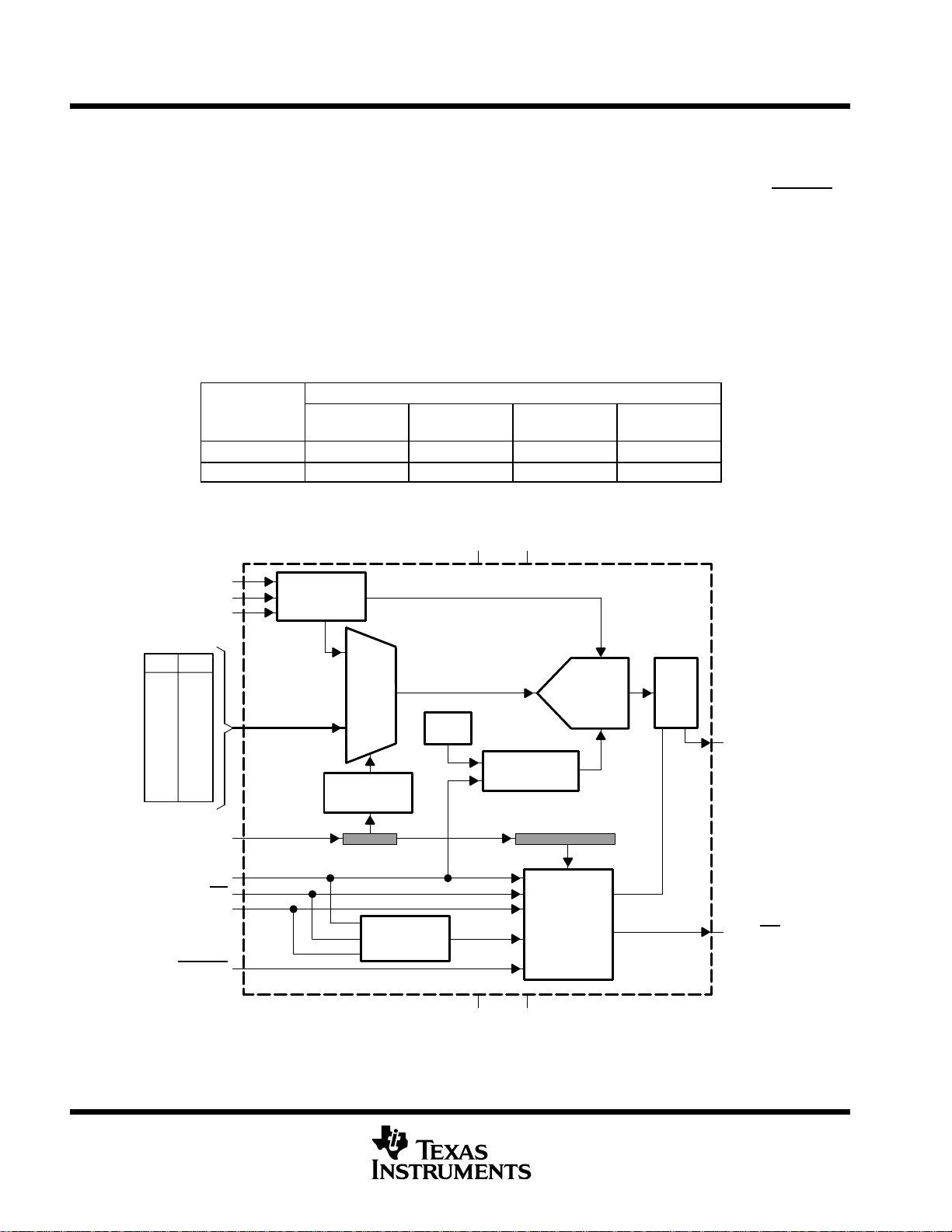
functional block diagram
REFP
BGAP
REFM
X4
X8
A0
A0
A1
A1
A2
A2
A3
A3
X
A4
X
A5
X
A6
X
A7
SDI
SCLK
CS
FS
CSTART
4-V
Reference
Command
CMR (4 MSBs)
Analog
MUX
Decode
4-Bit
Counter
OSC
DVDDAV
Conversion
DD
Clock
Control
Logic
SAR
ADC
CFR
FIFO
X8
SDO
EOC/INT
DGND AGND
2
POST OFFICE BOX 655303 • DALLAS, TEXAS 75265
Page 3
5-V ANALOG, 3-/5-V DIGITAL, 14-BIT, 200-KSPS, 4-/8-CHANNELS SERIAL
I/O
DESCRIPTION
ANALOG-TO-DIGITAL CONVERTERS WITH 0-5 V (PSEUDODIFFERENTIAL) INPUTS
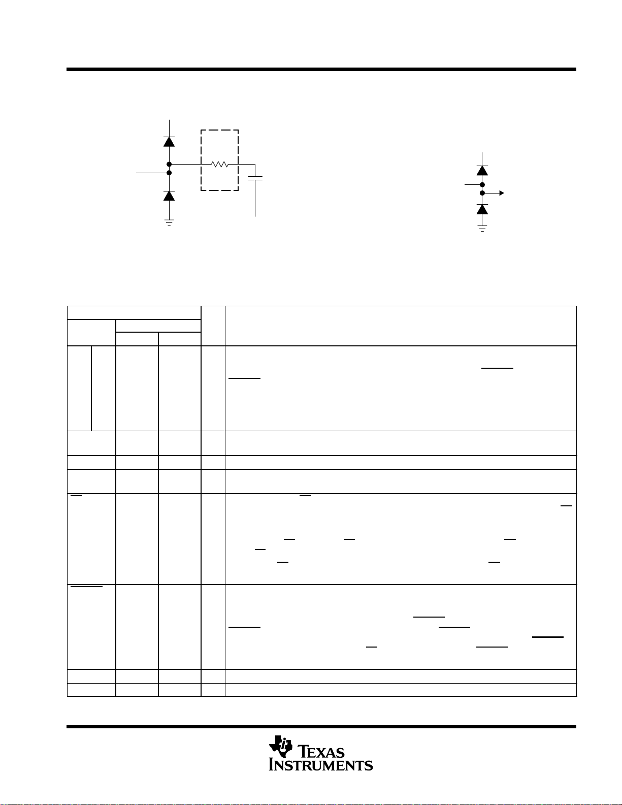
equivalent input circuit
V
DD
TLC3544, TLC3548
SLAS266C – OCTOBER 2000 – REVISED MAY 2003
MUX
1.1 kΩ
Max
Ain
Diode Turn on Voltage: 35 V
Equivalent Analog Input Circuit
R
on
REFM
C
(sample)
= 30 pF Max
Digital Input
Equivalent Digital Input Circuit
V
DD
Terminal Functions
TERMINAL
NAME
A0
A1
A2
A3
AGND 14, 18 18, 22 I Analog ground return for the internal circuitry. Unless otherwise noted, all analog voltage
AV
DD
BGAP 17 21 I Internal bandgap compensation pin. Install compensation capacitors between BGAP and AGND.
CS 8 8 I Chip select. When CS is high, SDO is in high-impedance state, SDI is ignored, and SCLK is
CSTART 20 24 I External sampling trigger signal, which initiates the sampling from a selected analog input channel
DGND 6 6 I Digital ground return for the internal circuitry
DV
DD
TLC3544 TLC3548
A0
A1
A2
A3
A4
A5
A6
A7
NO.
9
10
11
12
13, 19 17, 23 I Analog supply voltage
7 7 I Digital supply voltage
10
11
12
13
14
15
16
I/O DESCRIPTION
9
I Analog signal inputs. Analog input signals applied to these terminals are internally multiplexed. The
driving source impedance should be less than or equal to 1 kΩ for normal sampling. For larger
source impedance, use the external hardware conversion start signal CSTART (the low time of
CSTART
time.
measurements are with respect to AGND.
0.1 µF for external reference; 10 µF in parallel with 0.1 µF for internal reference.
disabled to clock data but works as conversion clock source if programmed. The falling edge of CS
input resets the internal 4-bit counter, enables SDI and SCLK, and removes SDO from
high-impedance state.
If FS is high at CS
select (SS
If FS is low at CS
select to allow the host to access the individual converter.
when the device works in extended sampling mode (asynchronous sampling). A high-to-low
transition starts the sampling of the analog input signal. A low-to-high transition puts the S/H in hold
mode and starts the conversion. The low time of the CST ART
CSTART
after the low-to-high transition for the conversion to finish maturely. The activation of CSTART
independent of SCLK and the level of CS
before the rising edge of the 1 1th SCLK. Tie this terminal to DVDD if not used.
controls the sampling period) or reduce the frequency of SCLK to increase the sampling
falling edge, CS falling edge initiates the operation cycle. CS works as slave
) to provide an SPI interface.
falling edge, FS rising edge initiates the operation cycle. CS can be used as chip
signal must be long enough for proper sampling. CSTART must stay high long enough
signal controls the sampling period.
is
and FS. However, the first CSTART cannot be issued
POST OFFICE BOX 655303 • DALLAS, TEXAS 75265
3
Page 4
TLC3544, TLC3548
I/O
DESCRIPTION
5-V ANALOG, 3-/5-V DIGITAL, 14-BIT, 200-KSPS, 4-/8-CHANNELS SERIAL
ANALOG-TO-DIGITAL CONVERTERS WITH 0-5 V (PSEUDODIFFERENTIAL) INPUTS
SLAS266C – OCTOBER 2000 – REVISED MAY 2003
Terminal Functions (Continued)
TERMINAL
NAME
EOC(INT) 4 4 O End of conversion (EOC) or interrupt to host processor (INT)
FS 2 2 I Frame sync input from DSP. The rising edge of FS indicates the start of a serial data frame being
REFM 16 20 I External low reference input. Connect REFM to AGND.
REFP 15 19 I External positive reference input. When an external reference is used, the range of maximum input
SCLK 1 1 I Serial clock input from the host processor to clock in the input from SDI and clock out the output
SDI 3 3 I Serial data input. The first 4 MSBs, ID[15:12], are decoded as one 4-bit command. All trailing bits,
SDO 5 5 O The 3-state serial output for the A/D conversion result. All data bits are shifted out through SDO.
TLC3544 TLC3548
NO.
I/O DESCRIPTION
EOC: used in conversion mode 00 only. EOC goes from high to low at the end of the sampling and
remains low until the conversion is complete and data is ready .
INT
: Interrupt to the host processor. The falling edge of INT indicates data is ready for output. INT
is cleared by the following CS↓, FS↑, or CSTART↓.
transferred (coming into or being sent out of the device). If FS is low at the falling edge of CS
rising edge of FS initiates the operation cycle, resets the internal 4-bit counter, and enables SDI,
SDO, and SCLK. Tie this pin to DVDD if FS is not used to initiate the operation cycle.
voltage is determined by the difference between the voltage applied to this terminal and to the
REFM terminal. Always install decoupling capacitors (10 µF in parallel with 0.1 µF) between REFP
and REFM.
via SDO. It can also be used as the conversion clock source when the external conversion clock
is selected (see Table 2). When CS is low, SCLK is enabled. When CS is high, SCLK is disabled
for the data transfer, but can still work as the conversion clock source.
except for the CONFIGURE WRITE command, are filled with zeros. The CONFIGURE WRITE
command requires additional 12-bit data. The MSB of input data, ID[15], is latched at the first falling
edge of SCLK following FS falling edge, if FS starts the operation, or latched at the falling edge of
first SCLK following CS
The remaining input data (if any) is shifted in on the rising edge of SCLK and latched on the falling
edge of SCLK. The input via SDI is ignored after the 4-bit counter counts to 16 (clock edges) or a
low-to-high transition of CS
requirements. Tie SDI to DVDD if using hardware default mode (refer to device initialization).
SDO is in the high-impedance state when CS
output format is MSB (OD[15]) first.
When FS initiates the operation, the MSB of output via SDO, OD[15], is valid before the first falling
edge of SCLK following the falling edge of FS.
When CS
following the CS
The remaining data bits are shifted out on the rising edge of SCLK and are valid before the falling
edge of SCLK. Refer to the timing specification for the details.
In a select/conversion operation, the first 14 bits are the results from the previous conversion (data).
In READ FIFO operation, the data is from FIFO. In both cases, the last two bits are don’t care.
In a WRITE operation, the output from SDO is ignored.
SDO goes into high-impedance state at the sixteenth falling edge of SCLK after the operation cycle
is initiated. SDO is in high-impedance state during conversions in modes 01, 10, and 11.
initiates the operation, the MSB, OD[15], is valid before the first falling edge of SCLK
falling edge when CS initiates the operation.
, whichever happens first. Refer to the timing specification for the timing
is high. SDO is released after a CS falling edge. The
falling edge.
, the
4
POST OFFICE BOX 655303 • DALLAS, TEXAS 75265
Page 5

TLC3544, TLC3548
5-V ANALOG, 3-/5-V DIGITAL, 14-BIT, 200-KSPS, 4-/8-CHANNELS SERIAL
ANALOG-TO-DIGITAL CONVERTERS WITH 0-5 V (PSEUDODIFFERENTIAL) INPUTS
SLAS266C – OCTOBER 2000 – REVISED MAY 2003
absolute maximum ratings over operating free-air temperature (unless otherwise noted)
Supply voltage, GND to AV
Analog input voltage range –0.2 V to AV
, DVDD –0.3 V to 6.5 V. . . . . . . . . . . . . . . . . . . . . . . . . . . . . . . . . . . . . . . . . . . . . . . .
DD
†
DD
+0.2 V. . . . . . . . . . . . . . . . . . . . . . . . . . . . . . . . . . . . . . . . . . . . . . . . . .
Analog input current 100 mA MAX. . . . . . . . . . . . . . . . . . . . . . . . . . . . . . . . . . . . . . . . . . . . . . . . . . . . . . . . . . . . . . . .
Reference input voltage AV
Digital input voltage range –0.3 V to DV
Operating virtual junction temperature range, T
Operating free-air industrial temperature range, T
–40°C to 150°C. . . . . . . . . . . . . . . . . . . . . . . . . . . . . . . . . . . .
J
:I suffix –40°C to 85°C. . . . . . . . . . . . . . . . . . . . . . . . . . . . .
A
DD
DD
+ 0.3 V. . . . . . . . . . . . . . . . . . . . . . . . . . . . . . . . . . . . . . . . . . . . . . . . . . . . . . . . . . . .
+ 0.3 V. . . . . . . . . . . . . . . . . . . . . . . . . . . . . . . . . . . . . . . . . . . . . . . . .
C suffix 0°C to 70°C. . . . . . . . . . . . . . . . . . . . . . . . . . . . . .
Storage temperature range, T
–65°C to 150°C. . . . . . . . . . . . . . . . . . . . . . . . . . . . . . . . . . . . . . . . . . . . . . . . . . .
stg
Lead temperature 1,6 mm (1.16 inch) from case for 10 seconds 260°C. . . . . . . . . . . . . . . . . . . . . . . . . . . . . . .
†
Stresses beyond those listed under “absolute maximum ratings” may cause permanent damage to the device. These are stress ratings only, and
functional operation of the device at these or any other conditions beyond those indicated under “recommended operating conditions” is not
implied. Exposure to absolute-maximum-rated conditions for extended periods may affect device reliability.
POST OFFICE BOX 655303 • DALLAS, TEXAS 75265
5
Page 6
TLC3544, TLC3548
VILLow level control in ut voltage
High level digital out ut
Low level digital out ut
OL
Off state out ut current
y
Power su ly
Autopower-down power supply
5-V ANALOG, 3-/5-V DIGITAL, 14-BIT, 200-KSPS, 4-/8-CHANNELS SERIAL
ANALOG-TO-DIGITAL CONVERTERS WITH 0-5 V (PSEUDODIFFERENTIAL) INPUTS
SLAS266C – OCTOBER 2000 – REVISED MAY 2003
general electrical characteristics over recommended operating free-air temperature range,
single-ended input, normal long sampling, 200 KSPS, AVDD = 5 V , external reference (V
V
= 0 V) or internal reference, SCLK frequency = 25 MHz, fixed channel at CONV mode 00,
REFM
analog input signal source resistance = 25 Ω (unless otherwise noted)
PARAMETER TEST CONDITIONS MIN TYP†MAX UNIT
Digital Input
V
IH
V
I
IH
I
IL
Digital output
V
OH
V
OL
I
OZ
Power Supply
AV
DD
DV
DD
I
CC
I
CC(SW)
I
CC(Autodown)
Operating temperature
†
All typical values are at TA = 25°C.
High-level control input voltage
Low-level control input voltage
High-level input current VI = DV
Low-level input current VI = DGND –2.5 0.005 µA
Input capacitance 20 25 pF
High-level digital output,
VOH at 30-pF load
Low-level digital output,
VOL at 30-pF load
Off-state output current
(high-impedance state)
pp
Supply voltage
Power suppl
current
Software power-down power supply current
p
current
-
p
,
,
AVDD currentAI
CC
DVDD currentDI
CC
p
pp
DVDD = 5 V 3.8
DVDD = 3 V
DVDD = 5 V 0.8
DVDD = 3 V 0.6
DD
IO = –0.2 mA
DVDD = 5 V
DVDD = 3 V
VO = DV
VO = DGND
Conversion clock is internal OSC,
EXT. reference, A VDD = 5.5 V to 4.5 V,
= DGND
CS
For all digital inputs DVDD or
DGND, CS = DVDD,
AVDD = 5.5 V
For all digital inputs DVDD or
DGND, AVDD = 5.5 V,
External reference
C suffix 0 70
I suffix –40 85
DVDD = 5 V 4.2
DVDD = 3 V 2.4
IO = 0.8 mA 0.4
IO = 50 µA 0.1
IO = 0.8 mA 0.4
IO = 50 µA 0.1
DD
CS = DV
DD
SCLK ON 175 240
SCLK OFF 20
SCLK ON 175 230
SCLK OFF 20
2.1
0.005 2.5 µA
0.02 1
–1 –0.02
4.5 5 5.5 V
2.7 5 5.5 V
2.8 3.6
1.2 2
REFP
= 4 V ,
V
V
V
V
µA
mA
µA
µA
°C
6
POST OFFICE BOX 655303 • DALLAS, TEXAS 75265
Page 7
TLC3544, TLC3548
5-V ANALOG, 3-/5-V DIGITAL, 14-BIT, 200-KSPS, 4-/8-CHANNELS SERIAL
ANALOG-TO-DIGITAL CONVERTERS WITH 0-5 V (PSEUDODIFFERENTIAL) INPUTS
SLAS266C – OCTOBER 2000 – REVISED MAY 2003
general electrical characteristics over recommended operating free-air temperature range,
single-ended input, normal long sampling, 200 KSPS, AVDD = 5 V , external reference (V
V
= 0 V) or internal reference, SCLK frequency = 25 MHz, fixed channel at CONV mode 00,
REFM
analog input signal source resistance = 25 Ω (unless otherwise noted) (continued)
PARAMETER TEST CONDITIONS MIN TYP
Resolution 14 bits
Analog Input
Voltage range 0 Reference V
Leakage current 0.01 0.05 µA
Capacitance 30 pF
Reference
Internal reference voltage 3.85 4 4.07 V
Internal reference temperature
coefficient
Internal reference source current 1.8 2.5 mA
Internal reference startup time 20 ms
V
REFP
V
REFM
Throughput Rate
f Internal oscillation frequency DVDD = 2.7 V to 5.5 V 6.5 MHz
t
(conv)
DC Accuracy—Normal Long Sampling
E
L
E
D
E
O
E
(g+)
†
All typical values are at TA = 25°C.
NOTES: 1. Conversion time t
External positive reference voltage 3 5 V
External negative reference voltage 0 AGND V
No conversion (AVDD = 5 V,
CS
= DVDD, SCLK = DGND)
External reference input impedance
External reference current
Conversion time
Acquisition time Normal short sampling 1.2 µs
Throughput rate (see Note 2)
Integral linearity error See Note 3 –1 ±0.5 1 LSB
Differential linearity error –1 ±0.5 1 LSB
Zero offset error See Note 4 –3 ±0.6 3 LSB
Gain error See Note 4 0 5 12 LSB
= (18x4 / SCLK) + 15 ns.
2. This is for a fixed channel in conversion mode 00 or 01. When switching the channels, additional multiplexer setting time is required
to overcome the memory effect of the charge redistribution DAC (refer to Figure 8).
3. Linear error is the maximum deviation from the best fit straight line through the A/D transfer characteristics.
4. Zero offset error is the difference between 0000000000000 and the converted output for zero input voltage; gain error is the
difference between 1 1111111111111 and the converted output for full-scale input voltage. The full-scale input voltage is equal to the
reference voltage being used.
(conv)
Normal long sampling (AVDD = 5 V,
= DGND, SCLK = 25 MHz,
CS
External conversion clock)
No conversion (V
V
= AGND, External reference,
REFM
CS = DVDD)
Normal long sampling (AVDD = 5 V,
CS
= DGND, SCLK = 25 MHz external
conversion clock at V
Internal OSC, 6.5 MHz minute 2.785
Conversion clock is external source,
SCLK = 25 MHz (see Note 1)
Normal long sampling, fixed channel in mode
00 or 01
= AVDD = 5 V,
REFP
REF
= 5 V)
100 MΩ
8.3 12.5 kΩ
200 KSPS
†
100 ppm/°C
1.5 µA
0.4 0.6 mA
2.895
= 4 V ,
REFP
MAX UNIT
µs
POST OFFICE BOX 655303 • DALLAS, TEXAS 75265
7
Page 8
TLC3544, TLC3548
5-V ANALOG, 3-/5-V DIGITAL, 14-BIT, 200-KSPS, 4-/8-CHANNELS SERIAL
ANALOG-TO-DIGITAL CONVERTERS WITH 0-5 V (PSEUDODIFFERENTIAL) INPUTS
SLAS266C – OCTOBER 2000 – REVISED MAY 2003
general electrical characteristics over recommended operating free-air temperature range,
single-ended input, normal long sampling, 200 KSPS, AVDD = 5 V , external reference (V
V
= 0 V) or internal reference, SCLK frequency = 25 MHz, fixed channel at CONV mode 00,
REFM
analog input signal source resistance = 25 Ω (unless otherwise noted) (continued)
PARAMETER TEST CONDITIONS MIN TYP†MAX UNIT
DC Accuracy—Normal Short Sampling
E
L
E
D
E
O
E
(g+)
AC Accuracy—Normal Long Sampling
SINAD Signal-to-noise ratio + distortion
THD Total harmonic distortion
SFDR Spurious free dynamic range
ENOB Effective number of bits
SNR Signal-to-noise ratio
AC Accuracy—Normal Short Sampling
SINAD Signal-to-noise ratio + distortion
THD Total harmonic distortion
SNR Signal-to-noise ratio
ENOB Effective number of bits
SFDR Spurious free dynamic range
†
All typical values are at TA = 25°C.
NOTES: 2. This is for a fixed channel in conversion mode 00 or 01. When switching the channels, additional multiplexer setting time is required
Integral linearity error See Note 3 ±0.8 LSB
Differential linearity error ±0.6 LSB
Zero offset error See Note 4 –3 ±0.6 3 LSB
Gain error See Note 4 0 5 12 LSB
fi = 20 kHz 78.6 80.8
fi = 100 kHz
fi = 20 kHz –95 –90
fi = 100 kHz
p
Channel-to-channel isolation (see
Notes 2 and 5)
Analog input bandwidth
Channel-to-channel isolation (see
Notes 2 and 5)
Analog input bandwidth
3. Linear error is the maximum deviation from the best fit straight line through the A/D transfer characteristics.
4. Zero offset error is the difference between 0000000000000 and the converted output for zero input voltage; gain error is the
5. It is measured by applying a full-scale of 35 kHz signal to other channels and determining how much the signal is attenuated in the
p
p
p
to overcome the memory effect of the charge redistribution DAC (refer to Figure 8).
difference between 1 1111111111111 and the converted output for full-scale input voltage. The full-scale input voltage is equal to the
reference voltage being used.
channel of interest. The converter samples this examined channel continuously . The channel-to-channel isolation is degraded if the
converter samples different channels alternately (refer to Figure 8).
fi = 20 kHz 90 97
fi = 100 kHz
fi = 20 kHz 12.8 13.1
fi = 100 kHz
fi = 20 kHz 79 81
fi = 100 kHz
Fixed channel in conversion mode 00, fi = 35 kHz 100 dB
Full power bandwidth, –1 dB 2
Full power bandwidth, –3 dB
fi = 20 kHz 78.9
fi = 100 kHz
fi = 20 kHz –95
fi = 100 kHz
fi = 20 kHz 79
fi = 100 kHz
fi = 20 kHz 12.8
fi = 100 kHz
fi = 20 kHz 97
fi = 100 kHz
Fixed channel in conversion mode 00, fi = 35 kHz 100 dB
Full power bandwidth, –1 dB 2
Full power bandwidth, –3 dB 2.5
77.6
–88
89
12.6
78
2.5
77.6
–88
78
12.6
89
REFP
= 4V ,
dB
dB
dB
Bits
dB
MHz
dB
dB
dB
Bits
dB
MHz
8
POST OFFICE BOX 655303 • DALLAS, TEXAS 75265
Page 9
TLC3544, TLC3548
g
Delay time, new SDO valid (reaches 90% of final level) after SCLK rising
5-V ANALOG, 3-/5-V DIGITAL, 14-BIT, 200-KSPS, 4-/8-CHANNELS SERIAL
ANALOG-TO-DIGITAL CONVERTERS WITH 0-5 V (PSEUDODIFFERENTIAL) INPUTS
SLAS266C – OCTOBER 2000 – REVISED MAY 2003
timing requirements over recommended operating free-air temperature range, A VDD = 5 V, DV
= 5 V, V
SCLK, SDI, SDO, EOC and INT
t
Cycle time of SCLK at 25-pF load
c(1)
t
Pulse width, SCLK high time at 25-pF load 40% 60% t
w(1)
t
Rise time for INT, EOC at 10-pF load
r(1)
t
Fall time for INT, EOC at 10-pF load
f(1)
Setup time, new SDI valid (reaches 90% final level) before falling edge of SCLK, at 25-pF
t
su(1)
load
Hold time, old SDI hold (reaches 10% of old data level) after falling edge of SCLK, at
t
h(1)
25-pF load
Delay time, new SDO valid (reaches 90% of final level) after SCLK risin
t
d(1)
edge, at 10-pF load
Hold time, old SDO hold (reaches 10% of old data level) after SCLK rising edge, at 10-pF
t
h(2)
load
Delay time, delay from sixteenth SCLK falling edge to EOC falling edge, normal sampling,
td(2)
at 10-pF load
Delay time, delay from the sixteenth falling edge of SCLK to INT falling edge, at 10-pF
t
d(3)
load [see the (‡) double dagger note and Note 6]
†
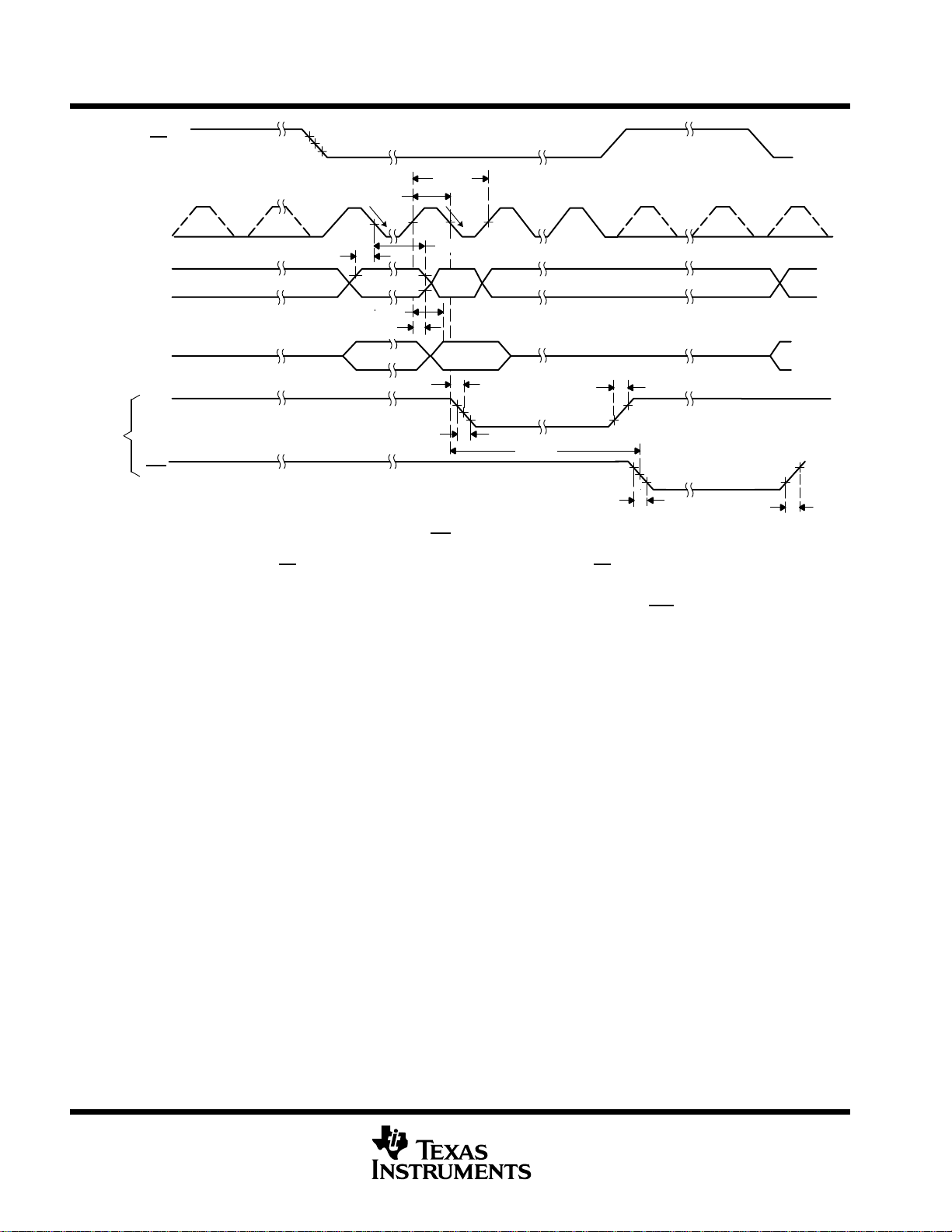
The minimum pulse width of SCLK high is 12.5 ns. The minimum pulse width of SCLK low is 12.5 ns.
‡
Specified by design
NOTE 6: For normal short sampling, t
= 5 V, V
REFP
For normal long sampling, t
Conversion time, t
SCLK is conversion clock source.
(conv)
= 0 V, SCLK frequency = 25 MHz (unless otherwise noted)
REFM
p
d(3)
d(3)
is equal to 18 × OSC + 15 ns when using internal OSC as conversion clock, or 72 × t
PARAMETERS MIN TYP MAX UNIT
DVDD = 2.7 V 100
DVDD = 5 V
DVDD = 5 V 6
DVDD = 2.7 V
DVDD = 5 V 6
DVDD = 2.7 V
DVDD= 5 V 0 10
DVDD = 2.7 V
is the delay from 16th falling edge of SCLK to INT
is the delay from 48th falling edge of SCLK to the falling edge of INT
falling edge.
†
40
6 – ns
0 – ns
0 23
0 – ns
0 6 ns
t
(conv)
.
t
(conv)
+ 15 ns when external
c(1)
c(1)
10
10
‡
+ 6 µs
DD
ns
ns
ns
ns
POST OFFICE BOX 655303 • DALLAS, TEXAS 75265
9
Page 10
TLC3544, TLC3548
5-V ANALOG, 3-/5-V DIGITAL, 14-BIT, 200-KSPS, 4-/8-CHANNELS SERIAL
ANALOG-TO-DIGITAL CONVERTERS WITH 0-5 V (PSEUDODIFFERENTIAL) INPUTS
SLAS266C – OCTOBER 2000 – REVISED MAY 2003
90%
t
su(1)
50%
10%
t
w(1)
ID15
t
t
h(2)
OD15
1
d(1)
ID1
OD1
t
f(1)
t
c(1)
t
h(1)
16
OD0
t
d(2)
See Note A
t
See Note B
d(3)
Don’t Care
t
r(1)
Hi-Z
OR
CS
SCLK
SDI
SDO
EOC
INT
Don’t Care ID0
Hi-Z
V
IH
V
IL
NOTES: A. For normal long sampling, t
B. For normal long sampling, t
– – – – The dotted line means signal may or may not exist, depending on application. It must be ignored.
Normal sampling mode, CS
SDI) are inactive and are ignored.
Figure 1. Critical Timing for SCLK, SDI, SDO, EOC and INT
t
f(1)
is the delay time of EOC low after the falling edge of 48th SCLK.
d(2)
is the delay time of INT
d(3)
initiates the conversion, FS must be tied to high. When CS is high, SDO is in Hi-Z; all inputs (FS, SCLK,
low after the falling edge of 48th SCLK.
t
r(1)
10
POST OFFICE BOX 655303 • DALLAS, TEXAS 75265
Page 11
TLC3544, TLC3548
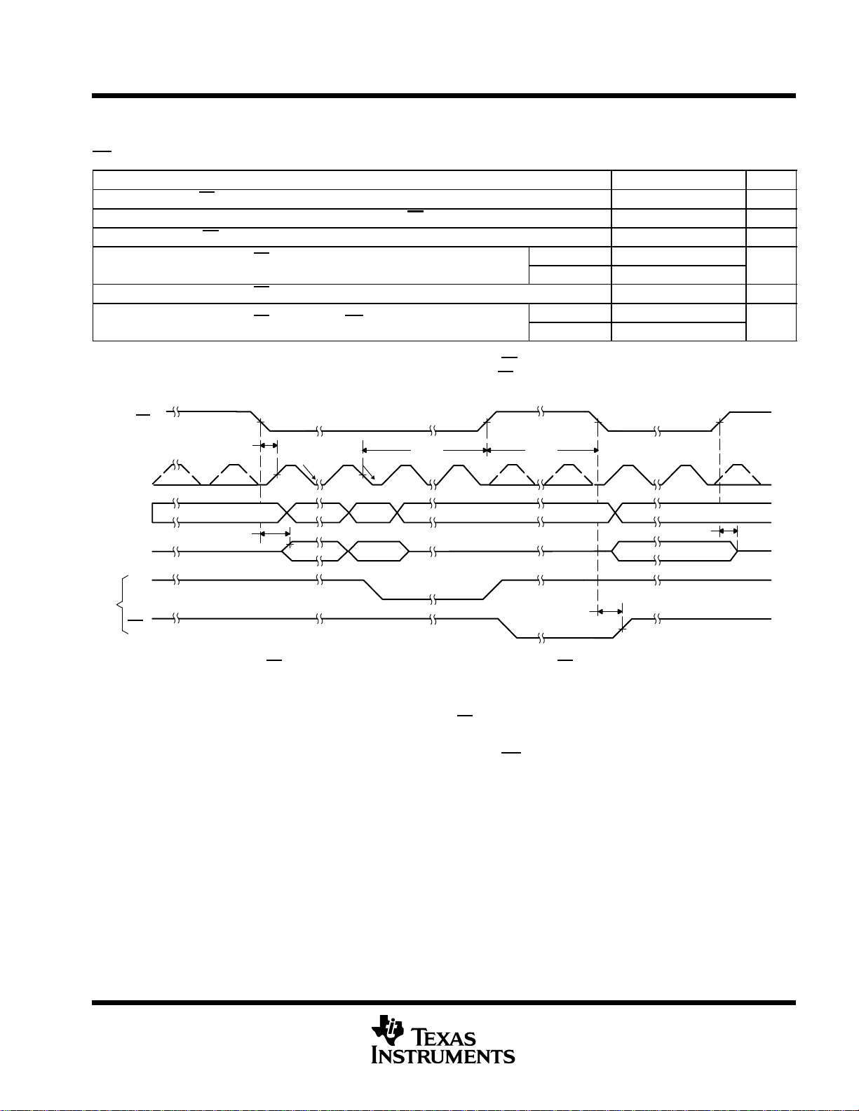
Delay time, delay from CS falling edge to MSB of SDO valid (reaches 90%
5-V ANALOG, 3-/5-V DIGITAL, 14-BIT, 200-KSPS, 4-/8-CHANNELS SERIAL
ANALOG-TO-DIGITAL CONVERTERS WITH 0-5 V (PSEUDODIFFERENTIAL) INPUTS
SLAS266C – OCTOBER 2000 – REVISED MAY 2003
timing requirements over recommended operating free-air temperature range, AVDD = 5 V,
DVDD = 5 V , V
CS trigger
t
Setup time, CS falling edge before SCLK rising edge, at 25-pF load 12 ns
su(2)
t
Delay time, delay time from 16th SCLK falling edge to CS rising edge, at 25-pF load
d(4)
t
Pulse width, CS high time at 25-pF load 1 t
w(2)
Delay time, delay from CS falling edge to MSB of SDO valid (reaches 90%
t
d(5)
final level), at 10-pF load
t
Delay time, delay from CS rising edge to SDO 3-state, at 10-pF load 0 6 ns
d(6)
t
Delay time, delay from CS falling edge to INT rising edge, at 10-pF load
d(7)
†
Specified by design
‡
For normal short sampling, td(4) is the delay time from 16th SCLK falling edge to CS
For normal long sampling, td(4) is the delay time from 48th SCLK falling edge to CS
CS
SCLK
REFP
= 5 V , V
t
su(2)
= 0 V , SCLK frequency = 25 MHz (unless otherwise noted) (continued)
REFM
PARAMETERS MIN TYP MAX UNIT
t
116
d(4)
‡
DVDD = 5 V 0 12
DVDD = 2.7 V
p
DVDD = 5 V 0 6
DVDD = 2.7 V 0 16
rising edge.
rising edge.
t
w(2)
5 ns
0 30
†
†
c(1)
ns
ns
V
IH
V
IL
SDI
SDO
EOC
OR
INT
NOTE A: – – – – The dotted line means signal may or may not exist, depending on application. It must be ignored.
Normal sampling mode, CS
SDI) are inactive and are ignored. Parts with date code earlier than 13XXXXX have these discrepancies:
(Date code is a 7 digit code next to the TI where the first digit indicates the year and the second digit is the month of production. 13,
in this case, is 2001 and the month of March.)
FS is not ignored even if the device is in microcontroller mode (CS
FS must be tied to DVDD.
Don’t Care ID0
t
d(5)
Hi-Z Hi-Z
ID15
ID1
OD1
OD15
initiates the conversion, FS must be tied to high. When CS is high, SDO is in Hi-Z, all inputs (FS, SCLK,
OD0
Don’t Care
triggered).
t
Don’t Care
d(7)
Figure 2. Critical Timing for CS Trigger
t
d(6)
Hi-Z
OD7OD15
POST OFFICE BOX 655303 • DALLAS, TEXAS 75265
11
Page 12
TLC3544, TLC3548
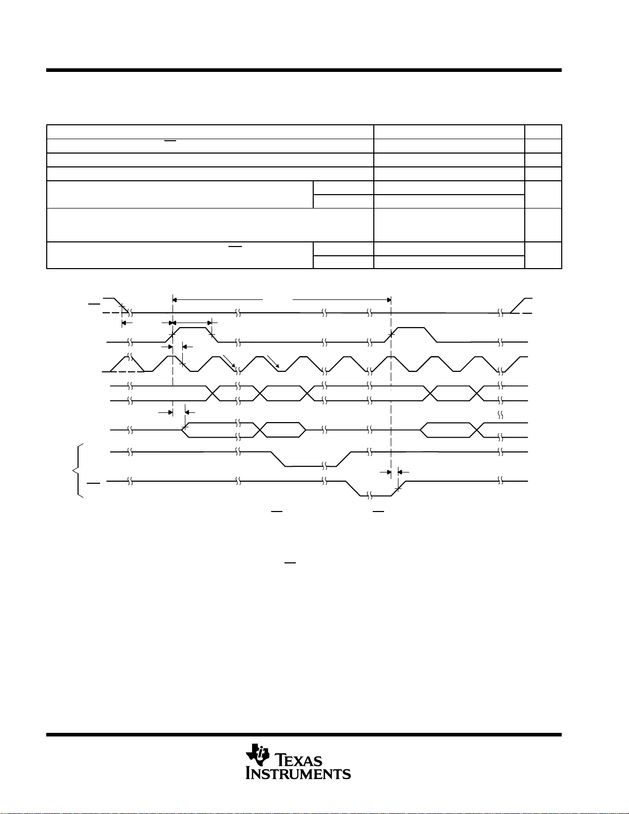
Delay time, delay from FS rising edge to MSB of SDO valid
Delay time, delay from FS rising edge to INT rising edge at
5-V ANALOG, 3-/5-V DIGITAL, 14-BIT, 200-KSPS, 4-/8-CHANNELS SERIAL
ANALOG-TO-DIGITAL CONVERTERS WITH 0-5 V (PSEUDODIFFERENTIAL) INPUTS
SLAS266C – OCTOBER 2000 – REVISED MAY 2003
timing requirements over recommended operating free-air temperature range, AVDD = 5 V,
DVDD = 5 V , V
FS trigger
t
Delay time, delay from CS falling edge to FS rising edge, at 25-pF load 0.5 t
d(8)
t
Setup time, FS rising edge before SCLK falling edge, at 25-pF load 0.25×t
su(3)
t
Pulse width, FS high at 25-pF load 0.75×t
w(3)
Delay time, delay from FS rising edge to MSB of SDO valid
t
d(9)
(reaches 90% final level) at 10-pF load
t
Delay time, delay from FS rising edge to next FS rising edge at 25-pF load
d(10)
Delay time, delay from FS rising edge to INT rising edge at
t
d(11)
10-pF load
†
Specified by design
REFP
= 5 V , V
= 0 V , SCLK frequency = 25 MHz (unless otherwise noted) (continued)
REFM
PARAMETERS MIN TYP MAX UNIT
t
c(1)
0.5×t
c(1)
c(1)
DVDD = 5 V 26
DVDD = 2.7 V
Required
sampling time +
conversion time
DVDD = 5 V 0 6
DVDD = 2.7 V 16
c(1)
1.25×t
+5 ns
c(1)
†
†
30
†
†
c(1)
ns
ns
µs
ns
t
ID1
OD1
d(10)
16
ID0Don’t Care ID15
OD0
can be tied to low. When CS is high, SDO is in Hi-Z, all inputs (FS, SCLK, SDI)
instead of FS rising edge in DSP mode (FS triggered).
Don’t Care Don’t Care
Hi-Z
t
d(11)
OD15
CS
t
su(3)
OD15
t
w(3)
1
ID15
t
d(8)
FS
SCLK
SDI
t
d(9)
SDO
EOC
OR
INT
NOTE A: – – – – The dotted line means signal may or may not exist, depending on application. It must be ignored.
Normal sampling mode, FS initiates the conversion, CS
are inactive and are ignored.
Parts with date code earlier than 13XXXXX have these discrepancies:
(Date code is a 7 digit code next to the TI where the first digit indicates the year and the second digit is the month of production. 13,
in this case, is 2001 and the month of March.)
SDO MSB (OD[15]) comes out from the falling edge of CS
Hi-Z
V
OH
V
OH
Figure 3. Critical Timing for FS Trigger
Don’t Care
V
IH
V
IL
12
POST OFFICE BOX 655303 • DALLAS, TEXAS 75265
Page 13

TLC3544, TLC3548
5-V ANALOG, 3-/5-V DIGITAL, 14-BIT, 200-KSPS, 4-/8-CHANNELS SERIAL
ANALOG-TO-DIGITAL CONVERTERS WITH 0-5 V (PSEUDODIFFERENTIAL) INPUTS
SLAS266C – OCTOBER 2000 – REVISED MAY 2003
timing requirements over recommended operating free-air temperature range, AVDD = 5 V,
DVDD = 5 V , V
CSTART trigger
t
d(12)
t
w(4)
t
d(13)
t
d(14)
t
d(15)
NOTES: 7. The pulse width of CSTART must be not less than the required sampling time. The delay from CSTART rising edge to following
Delay time, delay from CSTAR T rising edge to EOC falling
edge, at 10-pF load
Pulse width CSTAR T low time: t
Delay time, delay from CSTAR T rising edge to CSTART falling
edge, at 25-pF load
Delay time, delay from CSTAR T rising edge to INT falling edge,
at 10-pF load
Delay time, delay from CSTAR T falling edge to INT rising edge,
at 10-pF load
CSTART
is equal to the conversion time.
8. The maximum rate of SCLK is 25 MHz for normal long sampling and 10 MHz for normal short sampling.
= 5 V , V
REFP
PARAMETERS MIN TYP MAX UNIT
falling edge must not be less than the required conversion time. The delay from CSTAR T rising edge to the INT falling edge
= 0 V , SCLK frequency = 25 MHz (unless otherwise noted) (continued)
REFM
0 15 21 ns
(CSTART), at 25-pF load
W(L)
t
(sample – ref)
t
(conv)
t
(conv)
+0.4 Note 7 µs
+15 Notes 7 and 8 ns
+15 Notes 7 and 8 t
0 6 µs
(conv)
+21 ns
CSTART
OR
EOC
INT
t
w(4)
t
d(12)
Extended Sampling
t
d(14)
t
d(13)
t
(conv)
t
d(15)
Figure 4. Critical Timing for Extended Sampling (CSTART Trigger)
detailed description
converter
The converters are a successive-approximation ADC utilizing a charge redistribution DAC. Figure 5 shows a
simplified block diagram of the ADC. The sampling capacitor acquires the signal on Ain during the sampling
period. When the conversion process starts, the control logic directs the charge redistribution DAC to add and
subtract fixed amounts of charge from the sampling capacitor to bring the comparator into a balanced condition.
When balanced, the conversion is complete and the ADC output code is generated.
POST OFFICE BOX 655303 • DALLAS, TEXAS 75265
13
Page 14

TLC3544, TLC3548
5-V ANALOG, 3-/5-V DIGITAL, 14-BIT, 200-KSPS, 4-/8-CHANNELS SERIAL
ANALOG-TO-DIGITAL CONVERTERS WITH 0-5 V (PSEUDODIFFERENTIAL) INPUTS
SLAS266C – OCTOBER 2000 – REVISED MAY 2003
detailed description (continued)
Charge
Redistribution
DAC
REFM
_
+
Control
Logic
ADC Code
Ain
Figure 5. Simplified Block Diagram of the Successive-Approximation System
analog input range and internal test voltages
TLC3548 has eight analog inputs (TLC3544 has four) and three test voltages. The inputs are selected by the
analog multiplexer according to the command entered (see Table 1). The input multiplexer is a breakbefore-make type to reduce input-to-input noise injection resulting from channel switching.
The TLC3544 and TLC3548 are specified for a unipolar input range of 0-V to 4-V when the internal reference
is selected, and 0-V to 5-V when an external 5-V reference is used.
analog input mode
Two input signal modes can be selected: single-ended input and pseudodifferential input.
Charge
Redistribution
DAC
S1
Ain(+)
Ain(–)
_
+
Control
Logic
ADC Code
REFM
When sampling, S1 is closed and S2 connects to Ain(–).
During conversion, S1 is open and S2 connects to REFM.
Figure 6. Simplified Pseudodifferential Input Circuit
Pseudodifferential input refers to the negative input, Ain(–); its voltage is limited in magnitude to ±0.2 V . The input
frequency limit of Ain(–) is the same as the positive input Ain(+). This mode is normally used for ground noise
rejection or dc bias offset.
When pseudodifferential mode is selected, only two analog input channel pairs are available for the TLC3544
and four channel pairs for the TLC3548, because half the inputs are used as the negative input (see Figure 7).
14
POST OFFICE BOX 655303 • DALLAS, TEXAS 75265
Page 15

TLC3544, TLC3548
5-V ANALOG, 3-/5-V DIGITAL, 14-BIT, 200-KSPS, 4-/8-CHANNELS SERIAL
ANALOG-TO-DIGITAL CONVERTERS WITH 0-5 V (PSEUDODIFFERENTIAL) INPUTS
SLAS266C – OCTOBER 2000 – REVISED MAY 2003
analog input mode (continued)
Single Ended Pseudodifferential
‡
†
X4
X8
A0
A0
A1
A1
A2
A2
A3
A4
A5
A6
A7
†
TLC3548
‡
TLC3544
A3
X
X
X
X
Analog
MUX
SAR
ADC
Figure 7. Pin Assignment of Single-Ended Input vs Pseudodifferential Input
reference voltage
There is a built-in 4-V reference. If the internal reference is used, REFP is internally set to 4-V and REFM is set
to 0-V . The external reference can be applied to the reference-input pins (REFP and REFM) if programmed (see
T able 2). The REFM pin should connect to analog ground. REFP can be 3-V to 5-V . Install decoupling capacitors
(10 µF in parallel with 0.1 µF) between REFP and REFM. Install compensation capacitors (10 µF in parallel with
0.1 µF for internal reference, 0.1 µF only for external reference) between BGAP and AGND.
†
X8
A0(+) Pair A
A1(–)
A2(+) Pair B
A3(–)
A4(+) Pair C
A5(–)
A6(+) Pair D
A7(–)
X4‡
A0(+) Pair A
A1(–)
A2(+) Pair B
A3(–)
Analog
MUX
SAR
ADC
POST OFFICE BOX 655303 • DALLAS, TEXAS 75265
15
Page 16

TLC3544, TLC3548
5-V ANALOG, 3-/5-V DIGITAL, 14-BIT, 200-KSPS, 4-/8-CHANNELS SERIAL
ANALOG-TO-DIGITAL CONVERTERS WITH 0-5 V (PSEUDODIFFERENTIAL) INPUTS
SLAS266C – OCTOBER 2000 – REVISED MAY 2003
detailed description (continued)
ideal conversion characteristics
2s Complement
BTC
01111111111111
01111111111110
01111111111101
Binary
USB
11111111111111
11111111111110
11111111111101
16383
16382
16381
00000000000001
00000000000000
11111111111111
Digital Output Code
10000000000010
10000000000001
10000000000000
10000000000001
10000000000000
01111111111111
00000000000010
00000000000001
00000000000000
V
= VZS = 0 V
REFM
122 µV
244 µV
488 µV
1.999878 V 2.000122 V
VMS = (VFS + VZS)/2 = 2 V
Unipolar Analog Input Voltage
data format
INPUT DATA FORMAT (BINARY) OUTPUT DATA FORMAT READ CONVERSION/FIFO
MSB LSB MSB LSB
ID[15:12] ID[11:0] OD[15:2] OD[1:0]
Command Configuration data field or filled with zeros Conversion result Don’t Care
8193
8192
8191
2
1
0
V
REFP
VFS – 1 LSB = 3.999756 V
3.999512 V
Step
= VFS = 4 V
1 LSB = 244 µV
16
14-BIT
Unipolar Straight Binary Output: (USB)
Zero-scale code = VZS = 0000h, V
Mid-scale code = V
Full-scale code = V
UnIpolar Input, Binary 2’s Complement Output: (BTC)
Zero-scale code = V
Mid-scale code = V
Full-scale code = V
POST OFFICE BOX 655303 • DALLAS, TEXAS 75265
= 2000h, V
MS
= 3FFFh, V
FS
= 2000 h, V
ZS
= 0000h, V
MS
= 1FFFh, V
FS
code
code
code
code
code
code
= V
= V
= V
= V
= (V
= V
REFM
REFP
REFT
REFM
REFP
REFP
/2
– 1 LSB
– V
REFM
– 1 LSB
)/2
Page 17

TLC3544, TLC3548
5-V ANALOG, 3-/5-V DIGITAL, 14-BIT, 200-KSPS, 4-/8-CHANNELS SERIAL
ANALOG-TO-DIGITAL CONVERTERS WITH 0-5 V (PSEUDODIFFERENTIAL) INPUTS
SLAS266C – OCTOBER 2000 – REVISED MAY 2003
detailed description (continued)
operation description
The converter samples the selected analog input signal, then converts the sample into digital output, according
to the selected output format. The converter has four digital input pins (SDI, SCLK, CS
output pin (SDO) to communicate with the host device. SDI is a serial data input pin, SDO is a serial data output
pin, and SCLK is a serial clock from the host device. This clock is used to clock the serial data transfer. It can
also be used as the conversion clock source (see Table 2). CS
converter has a CSTART
for interrupt purposes.
device initialization
After power on, the status of EOC/INT
must be initialized before starting the conversion. The initialization procedure depends on the working mode.
The first conversion result is ignored after power on.
Hardware Default Mode: Nonprogrammed Mode, Default. After power on, two consecutive active cycles
initiated by CS
last 16 SCLKs at least. These cycles initialize the converter and load the CFR register with 800h (external
reference, unipolar straight binary output code, normal long sampling, internal OSC, single-ended input,
one-shot conversion mode, and EOC/INT
or FS put the device into hardware default mode if SDI is tied to DVDD. Each of these cycles must
pin for an external hardware sampling and conversion trigger, and an INT/EOC pin
is initially high, and the input data register is set to all zeros. The device
pin as INT). No additional software configuration is required.
and FS are used to start the operation. The
, and FS) and one digital
Software Programmed Mode: Programmed. When the converter has to be configured, the host must write
A000h into the converter first after power on, then perform the WRITE CFR operation to configure the device.
start of operation cycle
Each operation consists of several actions that the converter takes according to the command from the host.
The operation cycle includes three periods: command period, sampling period, and conversion period. In the
command period, the device decodes the command from the host. In the sampling period, the device samples
the selected analog signal according to the command. In the conversion period, the sample of the analog signal
is converted to digital format. The operation cycle starts from the command period, which is followed by one
or several sampling and conversion periods (depending on the setting) and finishes at the end of the last
conversion period.
The operation cycle is initiated by the falling edge of CS
Initiates The Operation: If FS is high at the falling edge of CS, the falling edge of CS initiates the operation.
CS
When CS
disabled to clock the serial data. The falling edge of CS
and SCLK. The MSB of the input data via SDI, ID[15], is latched at the first falling edge of SCLK following the
falling edge of CS
works as an SPI interface when CS
interface if CS
FS Initiates The Operation: If FS is low at the falling edge of CS
resets the internal 4-bit counter, and enables SDI, SDO, and SCLK. The ID[15] is latched at the first falling edge
of SCLK following the falling edge of FS. OD[15] is valid before this falling edge of SCLK. This mode is used
to interface the converter with a serial port of the host DSP . The FS of the device is connected to the frame sync
of the host DSP . When several devices are connected to one DSP serial port, CS
the host DSP to access each device individually. If only one converter is used, CS
is high, SDO is in the high-impedance state, the signals on SDI, and SDO are ignored, and SCLK is
. The MSB of output data from SDO, OD[15], is valid before this SCLK falling edge. This mode
is used as the slave select (SS). It also can be used as a normal DSP
connects to the frame sync output of the host DSP. FS must be tied high in this mode.
or the rising edge of FS.
resets the internal 4-bit counter and enables SDO, SDI,
, the rising edge of FS initiates the operation,
is used as chip select to allow
can be tied low.
After the initiation, the remaining SDI data bits (if any) are shifted in and the remaining bits of SDO (if any) are
shifted out at the rising edge of SCLK. The input data are latched at the falling edge of SCLK, and the output
data are valid before this falling edge of SCLK. After the 4-bit counter reaches 16, the SDO goes to a
high-impedance state. The output data from SDO is the previous conversion result in one shot conversion
mode, or the contents in the top of the FIFO when the FIFO is used (refer to Figure 21).
POST OFFICE BOX 655303 • DALLAS, TEXAS 75265
17
Page 18

TLC3544, TLC3548
5-V ANALOG, 3-/5-V DIGITAL, 14-BIT, 200-KSPS, 4-/8-CHANNELS SERIAL
ANALOG-TO-DIGITAL CONVERTERS WITH 0-5 V (PSEUDODIFFERENTIAL) INPUTS
SLAS266C – OCTOBER 2000 – REVISED MAY 2003
detailed description (continued)
command period
After the rising edge of FS (FS triggers the operation) or the falling edge of CS
(CS triggers the operation), SDI,
SDO, and SCLK are enabled. The first four SCLK clocks form the command period. The four MSBs of input data,
ID[15:12], are shifted in and decoded. These bits represent one of the 4-bit commands from the host, which
defines the required operation (see Table 1, Command Set). The four MSBs of output, OD[15:12], are also
shifted out via SDO during this period.
The commands are SELECT/CONVERSION, WRITE CFR, FIFO READ, SW POWER DOWN, and
HARDWARE DEFAULT mode. The SELECT/CONVERSION command includes SELECT ANALOG INPUT
and SELECT TEST commands. All cause a select/conversion operation. They select the analog signal being
converted, and start the sampling/conversion process after the selection. WRITE CFR causes the configuration
operation, which writes the device configuration information into the CFR register. FIFO READ reads the
contents in the FIFO. SW POWER DOWN puts the device into software power-down mode to save power.
Hardware default mode sets the device into the hardware default mode.
After the command period, the remaining 12 bits of SDI are written into the CFR register to configure the device
if the command is WRITE CFR. Otherwise, these bits are ignored. The configuration is retained in the
autopower-down and software power-down state. If SCLK stops (while CS
remains low) after the first eight bits
are entered, the next eight bits can be entered after SCLK resumes. The data on SDI are ignored after the 4-bit
counter counts to 16 (falling edge of SCLK) or the low-to-high transition of CS
, whichever happens first.
The remaining 12 bits of output data are shifted out from SDO if the command is SELECT/CONVERSION or
FIFO READ. Otherwise, the data on SDO are ignored. In any case, SDO goes into a high-impedance state after
the 4-bit counter counts to 16 (falling edge of SCLK) or the low-to-high transition of CS
, whichever happens first.
Table 1. Command Set (CMR)
SDI Bit D[15:12]
BINARY HEX
0000b 0h SELECT analog input channel 0 SELECT analog input channel 0
0001b 1h SELECT analog input channel 1 SELECT analog input channel 1
0010b 2h SELECT analog input channel 2 SELECT analog input channel 2
0011b 3h SELECT analog input channel 3 SELECT analog input channel 3
0100b 4h SELECT analog input channel 4 SELECT analog input channel 0
0101b 5h SELECT analog input channel 5 SELECT analog input channel 1
0110b 6h SELECT analog input channel 6 SELECT analog input channel 2
0111b 7h SELECT analog input channel 7 SELECT analog input channel 3
1000b 8h SW POWER DOWN
1001b 9h Reserved (test)
1010b Ah WRITE CFR, the last 12 bits of SDI are written into CFR. This command resets FIFO.
1011b Bh SELECT TEST, voltage = (REFP+REFM)/2 (see Notes 9 and 10)
1100b Ch SELECT TEST, voltage = REFM (see Note 11)
1101b Dh SELECT TEST, voltage = REFP (see Note 12)
1110b Eh FIFO READ, FIFO contents is shown on SDO; OD[15:2] = result, OD[1:0] = xx
1111b Fh Hardware default mode, CFR is loaded with 800h
NOTES: 9. REFP is external reference if external reference is selected, or internal reference if internal reference
is programmed.
10. The output code = mid-scale code + zero offset error + gain error.
11. The output code = zero scale code + zero offset error.
12. The output code = full-scale code + gain error.
TLC3548 COMMAND TLC3544 COMMAND
18
POST OFFICE BOX 655303 • DALLAS, TEXAS 75265
Page 19

5-V ANALOG, 3-/5-V DIGITAL, 14-BIT, 200-KSPS, 4-/8-CHANNELS SERIAL
[]
ANALOG-TO-DIGITAL CONVERTERS WITH 0-5 V (PSEUDODIFFERENTIAL) INPUTS
detailed description (continued)
Table 2. Configuration Register (CFR) Bit Definition
SDI BIT DEFINITION
D11 Reference select:
D10 Conversion output code format select:
D9 Sample period select for normal sampling
D8 Conversion clock source select:
D7
D[6:5] Conversion mode select:
D[4:3]
D2 EOC/INT pin function select:
D[1:0] FIFO trigger level (sweep sequence length). Don’t care in one shot mode.
0: Internal (4 V)
0: USB (unipolar straight binary)
0: Long sampling (4X) 44 SCLKs
0: Conversion clock = Internal OSC
Input mode select:
0: Single-ended
Pin Configuration of TLC3548 Pin Configuration of TLC3544
Pin No. Single-ended Pseudodifferential polarity Pin No. Single-ended Pseudodifferential polarity
9
10
11
12
13
14
15
16
00: One shot mode
01: Repeat mode
10: Sweep mode
11: Repeat sweep mode
Sweep auto sequence select (Note: These bits only take effect in conversion mode 10 and 1 1.)
Single ended(by ch) Pseudodifferential (by pair) Single ended (by ch) Pseudodifferential (by pair)
00: 0–1–2–3–4–5–6–7
01: 0–2–4–6–0–2–4–6
10: 0–0–2–2–4–4–6–6
11: 0–2–0–2–0–2–0–2
0: Pin used as INT
00: Full (INT
01: 3/4 (INT
10: 1/2 (INT
11: 1/4 (INT
A0
A1
A2
A3
A4
A5
A6
A7
generated after FIFO level 7 filled)
generated after FIFO level 5 filled)
generated after FIFO level 3 filled)
generated after FIFO level 1 filled)
PLUS
MINUS
PLUS
MINUS
PLUS
MINUS
PLUS
MINUS
TLC3548 TLC3544
00: N/A
01: A–B–C–D–A–B–C–D
10: A–A–B–B–C–C–D–D
11: A–B–A–B–A–B–A–B
1: External
1: Binary 2s complement
Don’t care in extended sampling.
1: Short sampling (1X) 12 SCLKs
1: Conversion clock = SCLK/4
1: Pseudodifferential. Pin configuration shown below.
Pair A 9
Pair B 11
Pair C
Pair D
1: Pin used as EOC ( for mode 00 only)
SLAS266C – OCTOBER 2000 – REVISED MAY 2003
10
12
00: 0–1–2–3–0–1–2–3
01: 0–2–0–2–0–2–0–2
10: 0–0–1–1–2–2–3–3
11: 0–0–0–0–2–2–2–2
A0
A1
A2
A3
TLC3544, TLC3548
PLUS
MINUS
PLUS
MINUS
00: N/A
01: A–B–A–B–A–B–A–B
10: N/A
11: A–A–A–A–B–B–B–B
Pair A
Pair B
sampling period
The sampling period follows the command period. The selected signal is sampled during this time. The device
has three different sampling modes: normal short mode, normal long mode, and extended mode.
Normal Short Sampling Mode: Sampling time is controlled by SCLK. It takes 12 SCLK periods. At the end of
sampling, the converter automatically starts the conversion period. After configuration, normal sampling, except
FIFO READ and WRITE CFR commands, starts automatically after the fourth falling edge of SCLK that follows
the falling edge of CS
if CS triggers the operation, or follows the rising edge of FS if FS initiates the operation.
POST OFFICE BOX 655303 • DALLAS, TEXAS 75265
19
Page 20

TLC3544, TLC3548
5-V ANALOG, 3-/5-V DIGITAL, 14-BIT, 200-KSPS, 4-/8-CHANNELS SERIAL
ANALOG-TO-DIGITAL CONVERTERS WITH 0-5 V (PSEUDODIFFERENTIAL) INPUTS
SLAS266C – OCTOBER 2000 – REVISED MAY 2003
sampling period (continued)
Normal Long Sampling Mode: This mode is the same as normal short sampling, except that it lasts 44 SCLK
periods.
Extended Sampling Mode: The external trigger signal, CST AR T
not used for sampling. SCLK is also not needed for conversion if the internal conversion clock is selected. The
falling edge of CSTART
CSTART
internal delay). The occurrence of CST AR T
CSTART
CSTART
sampling mode at the falling edge of CST ART
consecutive falling edges of CS
by a write CFR). The first CS
not suitable for sampling, or when an extended sampling period is needed to accommodate different input signal
source impedance.
conversion period
The conversion period is the third
for normal short sampling mode, or after the falling edge of the 48th SCLK for normal long sampling, or on the
rising edge of CSTART
is low. The rising edge of CSTART ends the sampling and starts the conversion (with about 15 ns
cannot occur before the rising edge of the 11th SCLK. In other words, the falling edge of the first
can happen at or after the rising edge of the 1 1th SCLK, but not before. The device enters the extended
begins the sampling of the selected analog input. The sampling continues while
is independent of the SCLK clock, CS, and FS. However, the first
and exits this mode once CST ART goes to high followed by two
or two consecutive rising edges of FS (such as one read data operation followed
or FS does not cause conversion. Extended mode is used when a fast SCLK is
portion of the operation cycle. It begins after the falling edge of the 16th SCLK
(with 15 ns internal delay) for extended sampling mode.
, triggers sampling and conversion. SCLK is
The conversion takes 18 conversion clocks plus 15 ns. The conversion clock source can be an internal oscillator,
OSC, or an external clock, SCLK. The conversion clock is equal to the internal OSC if the internal clock is used,
or equal to SCLK/4 when the external clock is programmed. T o avoid premature termination of the conversion,
enough time for the conversion must be allowed between consecutive triggers. EOC
of the conversion period and goes high at the end of the conversion period. INT
conversion mode
Four different conversion modes (mode 00, 01, 10, 11) are available. The operation of each mode is slightly
different, depending on how the converter samples and what host interface is used. Do not mix different types
of triggers throughout the repeat or sweep operations.
One Shot Mode (Mode 00): Each operation cycle performs one sampling and one conversion for the selected
channel. The FIFO is not used. When EOC
Otherwise, INT
next select/conversion operation.
Repeat Mode (Mode 01): Each operation cycle performs multiple samplings and conversions for a fixed
channel selected according to the 4-bit command. The results are stored in the FIFO. The number of samples
to be taken is equal to the FIFO threshold programmed via D[1:0] in the CFR register. Once the threshold is
reached, INT
replaced in the next operation. The operation of this mode starts with the WRITE CFR command to set
conversion mode 01, then the SELECT/CONVERSION command, followed by a number of samplings and
conversions of the fixed channel (triggered by CS
triggers the sampling, the data on SDI must be any one of the SELECT CHANNEL commands. This data is a
dummy code for setting the converter in the conversion state. It does not change the existing channel selection
set at the start of the operation until the FIFO is full. After the operation finishes, the host can read the FIFO,
then reselect the channel and start the next REPEA T operation again; or immediately reselect the channel and
start the next REPEAT operation (by issuing CS,
a new operation according to the new setting. If CST ART
start the next REPEA T (on the current channel) after the FIFO is full. Besides, if FS initiates the operation and
CSTART
the host to set up the converter, continue monitoring a fixed input, and to get a set of samples as needed.
is generated after the conversion is done. The result is output through the SDO pin during the
is generated, and the operation ends. If the FIFO is not read after the conversions, the data are
triggers the sampling and conversions, CS must not toggle during the conversion. This mode allows
is selected, it is generated while the conversion period is in progress.
, FS, or CST AR T) until the FIFO threshold is hit. If CS or FS
FS, or CSTAR), or reconfigure the converter and then start
triggers the sampling, the host can also immediately
goes low at the end of this period.
goes low at the beginning
20
POST OFFICE BOX 655303 • DALLAS, TEXAS 75265
Page 21

TLC3544, TLC3548
5-V ANALOG, 3-/5-V DIGITAL, 14-BIT, 200-KSPS, 4-/8-CHANNELS SERIAL
ANALOG-TO-DIGITAL CONVERTERS WITH 0-5 V (PSEUDODIFFERENTIAL) INPUTS
SLAS266C – OCTOBER 2000 – REVISED MAY 2003
conversion mode (continued)
Sweep Mode (Mode 10): During each operation, all of the channels listed in the sweep sequence (D[4:3] of
the CFR register) are sampled and converted at one time according to the programmed sequence. The results
are stored in the FIFO. When the FIFO threshold is reached, an interrupt (INT
ends. If the FIFO threshold is reached before all of the listed channels are visited, the remaining channels are
ignored. This allows the host to change the sweep sequence length. The mode 10 operation starts with the
WRITE CFR command to set the sweep sequence. The following triggers (CS
the interface) start the samplings and conversions of the listed channels in sequence until the FIFO threshold
is hit. If CS
or FS starts the sampling, the SDI data must be any one of the SELECT commands to set the
converter in the conversion state. However, this command is a dummy code. It does not change the existing
conversion sequence. After the FIFO is full, the converter waits for the FIFO READ. It does nothing before the
FIFO READ or the WRITE CFR command is issued. The host must read the FIFO completely or write the CFR.
If CST ART
channel) via CS
triggers the samplings, the host must issue an extra SELECT/CONVERSION command (select any
or FS after the FIFO READ or WRITE CFR. This extra period is named the arm period and is
used to set the converter into the conversion state, but does not affect the existing conversion sequence.
Besides, if FS initiates the operation and CST AR T
triggers the sampling and conversions, CS must not toggle
during the conversion.
Repeat Sweep Mode (Mode 11): This mode works in the same way as mode 10, except that it is not necessary
to read the FIFO before the next operation after the FIFO threshold is hit. The next SWEEP can repeat
immediately, but the contents in the FIFO are replaced by the new results. The host can read the FIFO
completely , then issue the next SWEEP or repeat the SWEEP immediately (with the existing sweep sequence)
by issuing sampling/conversion triggers (CS
, FS or CST ART) or change the device setting with the WRITE CFR.
The memory effect of charge redistribution DAC exists when the mux switches from one channel to another.
This degrades the channel-to-channel isolation if the channel changes after each conversion. For example, in
mode 10 and 1 1, the isolation is about 70 dB for the sweep sequence 0-1-2-3-4 (refer to Figure 8). The memory
effect can be reduced by increasing the sampling time or using the sweep sequence 0-0-2-2-4-4-6-6 and
ignoring the first sample of each channel. Figure 8 shows the typical isolation vs throughput rate when applying
a sine signal (35 kHz, 3.5 V
) on CH0 and dc on CH1 converting both channels alternately and measuring the
p-p
attenuation of the sine wave in CH1.
CHANNEL-TO-CHANNEL ISOLATION
vs
100
THROUGHPUT
) is generated, and the operation
, FS, or CST ART, depending on
90
80
70
Channel-to-Channel Isoltaion – dB
60
0 50 100 150 200
Throughput – KSPS
Figure 8
POST OFFICE BOX 655303 • DALLAS, TEXAS 75265
21
Page 22

TLC3544, TLC3548
5-V ANALOG, 3-/5-V DIGITAL, 14-BIT, 200-KSPS, 4-/8-CHANNELS SERIAL
ANALOG-TO-DIGITAL CONVERTERS WITH 0-5 V (PSEUDODIFFERENTIAL) INPUTS
SLAS266C – OCTOBER 2000 – REVISED MAY 2003
operation cycle timing
CS
Initiates
Operation
4 SCLKs
†
t
(setup)
SDI
4-bit Command 12-bit CFR Data (Optional)
44 SCLKs for Long
12 SCLKs for Short
t
(sample)
18 OSC for Internal OSC
72 SCLK for External Clock
t
(convert)
†
15 ns
t
(overhead)
SDO
Active CS
(FS Is Tied to High)
2-bit Don’t Care14-bit Data (Previous Conversion)
CSTAR (For Extended Sampling) occurs at
or after the rising edge of eleventh SCLK
FS Initiates
Operation
†
Non JEDEC terms used.
t
(delay)
4 SCLKs
†
4-bit Command 12-bit CFR Data (Optional)
SDI
SDO
14-bit Data (Previous Conversion)
Active FS
t
(setup)
Active CS
†
(CS Can Be Tied to Low)
CSTAR
44 SCLKs for Longt–CSL to FSL
(For Extended Sampling) occurs at
or after the rising edge of eleventh SCLK
12 SCLKs for Short
t
(sample)
2-bit Don’t Care
18 OSC for Internal OSC
72 SCLK for External Clock
t
(convert)
15 nS
t
(overhead)
After the operation is finished, the host has several choices. Table 3 summarizes operation options.
22
POST OFFICE BOX 655303 • DALLAS, TEXAS 75265
Page 23

5-V ANALOG, 3-/5-V DIGITAL, 14-BIT, 200-KSPS, 4-/8-CHANNELS SERIAL
ANALOG-TO-DIGITAL CONVERTERS WITH 0-5 V (PSEUDODIFFERENTIAL) INPUTS
operation cycle timing (continued)
TLC3544, TLC3548
SLAS266C – OCTOBER 2000 – REVISED MAY 2003
Table 3. Operation Options
MODE
00 1. Issue new Select/Read operation to
read data and start new conversion.
2. Reconfigure the device.
01 1. Read FIFO—Select Channel—Start
new conversion. Channel must be
selected after FIFO READ.
2. Select Channel—Start new
conversion (old data lost)
3. Configure device again.
10 1. Read FIFO—Start new conversion
with existing setting.
2. Configure device—New conversion
(old data lost)
11 1. Read FIFO—Start new conversion
with existing setting.
2. Start new conversion with the existing
setting.
3. Configure device—Start new
conversion with new setting.
CS FS CSTART
CONVERSION IS INITIATED BY
1. Issue new Select/Read operation to
read data and start new conversion.
2. Reconfigure the device.
1. Read FIFO—Select Channel—Start
new conversion. Channel must be
selected after FIFO READ.
2. Select Channel—Start new
conversion (old data lost)
3. Configure device again.
1. Read FIFO—Start new conversion
with existing setting.
2. Configure device—New conversion
(old data lost)
1. Read FIFO—Start new conversion
with existing setting
2. Start new conversion with the existing
setting.
3. Configure Device—Start new
conversion with new setting.
1. Issue new CSTART to start next
conversion; old data lost.
2. Issue new Select/Read operation to
read data—Issue new CSTAR T
start new conversion.
3. Reconfigure the device.
1. Read FIFO—Select channel—Start
new conversion. Channel must be
selected after FIFO READ.
2. Start new conversion (old data lost)
with existing setting.
3. Configure device again.
1. Read FIFO—Arm Period—Start new
conversion with existing setting
2. Configure device—Arm Period—New
conversion (old data lost)
1. Read FIFO—Arm Period—Start new
Conversion with existing setting
2. Start new conversion with existing
setting. (old data lost)
3. Configure device—Arm Period—New
conversion with new setting.
operation timing diagrams
The FIFO read and write CFR are nonconversion operations. The conversion operation performs one of four
types of conversion: mode 00, 01, 10, and 11
to
Write Cycle (WRITE CFR Command): Write cycle does not generate EOC or INT
conversion.
OR
CS
FS
SDI
INT
EOC
SDO
1
ID15 1D14 ID13 1D12
354
2
Note: Signal May Not Exist.
ID11 ID10 ID9 ID4 ID3 ID2 ID1 ID0
Don’t Care
7
6
12
13 14 15 16
Figure 9. Write Cycle, FS Initiates Operation
, nor does it carry out any
1
ID15
Hi-Z
POST OFFICE BOX 655303 • DALLAS, TEXAS 75265
23
Page 24

TLC3544, TLC3548
5-V ANALOG, 3-/5-V DIGITAL, 14-BIT, 200-KSPS, 4-/8-CHANNELS SERIAL
ANALOG-TO-DIGITAL CONVERTERS WITH 0-5 V (PSEUDODIFFERENTIAL) INPUTS
SLAS266C – OCTOBER 2000 – REVISED MAY 2003
operation timing diagrams (continued)
FS = High
OR
EOC
SDO
CS
SDI
INT
123 546
ID15 1D14 ID13 1D12
Note: Signal May Not Exist.
7
Don’t Care
13
12
14
15 16
Hi-Z
1
ID15
ID14ID11 ID10 ID9 ID4 ID3 ID2 ID1 ID0
Figure 10. Write Cycle, CS Initiates Operation, FS = 1
FIFO Read Operation: When the FIFO is used, the first command after INT
is generated is assumed to be the
FIFO read. The first FIFO content is sent out immediately before the command is decoded. If this command is
not a FIFO read, the output is terminated. Using more layers of the FIFO reduces the time taken to read multiple
conversion results, because the read cycle does not generate an EOC or INT
, nor does it make a data
conversion. Once the FIFO is read, the entire contents in the FIFO must be read out. Otherwise, the remaining
data is lost.
SCLK
1235467 13
12
14 15
16
1
FS = High
OR
EOC
SDO
CS
SDI
INT
ID15 1D14 ID13 1D12
OD15 OD14 OD13 OD12 OD15
Notes: Signal May Not Exist.
OD11 OD10 OD9 OD4 OD3 OD2
OD[15:2] is FIFO Contents.
Don’t Care
Hi-Z
ID15 ID14
Figure 11. FIFO Read Cycle, CS Initiates Operation, FS = 1
OD14
24
POST OFFICE BOX 655303 • DALLAS, TEXAS 75265
Page 25

ANALOG-TO-DIGITAL CONVERTERS WITH 0-5 V (PSEUDODIFFERENTIAL) INPUTS
conversion operation
123 5467 131415
CS
TLC3544, TLC3548
5-V ANALOG, 3-/5-V DIGITAL, 14-BIT, 200-KSPS, 4-/8-CHANNELS SERIAL
SLAS266C – OCTOBER 2000 – REVISED MAY 2003
48 SCLKs for Long Sampling
16 SCLKs for Short Sampling
12
16
1
FS in High
OR
SCLK
OR
SDI
INT
EOC
SDO
CS
FS
SDI
INT
EOC
SDO
Select Channel
ID15 ID14 ID13 1D12
t
(SAMPLE)
Previous Conversion Result
OD15 OD14 OD13 OD12 OD11 OD10 OD9 OD4
The dotted line means signal may or may not exist.
OD[15:2] is the result of previous conversion.
Don’t Care
OD3
Figure 12. Mode 00, CS Initiates Operation
48 SCLKs for Long Sampling
16 SCLKs for Short Sampling
123 5467 131415
Select Channel
ID15 1D14 ID13 1D12
Previous Conversion Result
OD14 OD13 OD12 OD11 OD10 OD9 OD4OD15 OD15OD2OD3
The dotted line means signal may or may not exist.
OD[15:2] is the result of previous conversion.
Don’t Care
SDO Goes Through Hi-Z After 16 SCLK
t
(SAMPLE)
12
ID15
t(conv)
OD2 OD15
SDO goes to Hi-Z After 16th SCLK
16
t
(conv)
Hi-Z
Hi-Z
1
ID15
Figure 13. Mode 00, FS Initiates Operation
POST OFFICE BOX 655303 • DALLAS, TEXAS 75265
25
Page 26

TLC3544, TLC3548
ÌÌ
5-V ANALOG, 3-/5-V DIGITAL, 14-BIT, 200-KSPS, 4-/8-CHANNELS SERIAL
ANALOG-TO-DIGITAL CONVERTERS WITH 0-5 V (PSEUDODIFFERENTIAL) INPUTS
SLAS266C – OCTOBER 2000 – REVISED MAY 2003
conversion operation (continued)
CS Tied to Low
Select Channel
16 SCLK
t
(sample)
Select Channel
16 SCLK
CSTART
OR
SDI
SDO
INT
FS
SDI
INT
EOC
Hi-Z
SDO
Possible Signal
** Select Channel
Don’t Care
Figure 14. Mode 00, CSTART Triggers Sampling/Conversion, FS Initiates Select
CS
FS
*** –– WRITE CFR
** –– Select Channel
* –– FIFO Read
Possible
Signal
**
***
Previous Conversion Result
Select CH1
*** *
Don’t Care
Possible Signal
**
Select Any
Channel
**
Hi-Z
1/4 FIFO FULL 1/4 FIFO FULL
DATA1 of CH1 DATA2 of CH1
MODE 01, FS Activates Conversion, FIFO Threshold = 1/4 Full
t
(convert)
Hi-Z
Data Lost
*
Read FIFO After Threshold Is Hit
Select CH2
**
Select Any
Channel
**
**
Conversion Result
*
DATA1 of CH2 DATA2 of CH2
Hi-Z
*
26
CS
FS
CSTART
SDI
SDO
INT
Select CH1 Select CH2
***
Don’t Care
Possible Signal
*** –– WRITE CFR
** –– Select Channel
* –– FIFO Read
Figure 16. Mode 01, CSTART Triggers Samplings/Conversions
Figure 15. Mode 01, FS Initiates Operations
**
Hi-Z
1/4 FIFO FULL
MODE 01, FS Initiates Select Period, CSTART
POST OFFICE BOX 655303 • DALLAS, TEXAS 75265
*
DATA1 of CH1 DATA2 of CH1 DATA1 of CH2 DATA2 of CH2
*
Read FIFO After Threshold Is Hit
**
1/4 FIFO FULL
Activates Conversion, FIFO Threshold = 1/4 Full,
*
*
Page 27

5-V ANALOG, 3-/5-V DIGITAL, 14-BIT, 200-KSPS, 4-/8-CHANNELS SERIAL
ANALOG-TO-DIGITAL CONVERTERS WITH 0-5 V (PSEUDODIFFERENTIAL) INPUTS
conversion operation (continued)
Configure
CS
FS
Conversion
From CH0
Conversion
From CH3
TLC3544, TLC3548
SLAS266C – OCTOBER 2000 – REVISED MAY 2003
Conversion
From CH0
Conversion
From CH3
SDI
***
** ** ** **
INT
SDO
Don’t Care
*** Command = Configure Write for Mode 10, FIFO
Threshold = 1/2 Full, Sweep Sequence: 0–1–2–3
** COMMAND = Select Any Channel
* COMMAND = Read FIFO
Hi-Z
1st Sweep
Figure 17. Mode 10, FS Initiates Operations
CS Tied
to Low
Configure
Conversion
From CH0
FS
CSTART
***
SDI
INT
SDO
Don’t Care
*** Command = Configure Write for Mode 10, FIFO
Threshold = 1/2 Full, Sweep Sequence: 0–0–2–2
** COMMAND = Select Any Channel
* COMMAND = Read FIFO
1st Sweep
Hi-Z
Conversion
From CH2
*
*
*
CH0 CH1 CH2 CH3
1st FIFO Read
Read FIFO After FIFO Threshold Is Hit
*
*
*
CH0 CH0 CH2 CH2
1st FIFO Read
Read FIFO After FIFO Threshold Is Hit, FS Initiates Select Period
** ** ** **
*
Using Existing
Configuration
Conversion
From CH0
*
**
Using Existing
Configuration
2nd Sweep
2nd Sweep
Conversion
From CH2
2nd FIFO Read
*
CH0
2nd FIFO Read
***
CH0
Figure 18. Mode 10, CSTART Initiates Operations
Configure
Conversion
From CH0
CS
FS=High
SDI
***
**** ** ** ** ** ** ** * * * * **
INT
SDO
Don’t Care
*** Command = Configure Write for Mode 11, FIFO
Threshold = 1/2 Full, Sweep Sequence: 0–1–2–3
** COMMAND = Select Any Channel
* COMMAND = Read FIFO
Conversion
From CH3
Figure 19. Mode 11, CS Initiates Operations
Conversion
From CH0
START 2nd Round SWEEP CONVERSION,
the DATA of the 1st Round Are Lost
START 2nd Sweep conversion immediately (NO FIFO READ) after the 1st SWEEP completed.
Conversion
From CH3
CH1 CH3CH2CH0
READ the DATA of 2nd
Sweep From FIFO
Conversion
From CH0
POST OFFICE BOX 655303 • DALLAS, TEXAS 75265
27
Page 28

TLC3544, TLC3548
TLC3544/48
()
5-V ANALOG, 3-/5-V DIGITAL, 14-BIT, 200-KSPS, 4-/8-CHANNELS SERIAL
ANALOG-TO-DIGITAL CONVERTERS WITH 0-5 V (PSEUDODIFFERENTIAL) INPUTS
SLAS266C – OCTOBER 2000 – REVISED MAY 2003
conversion operation (continued)
CS
FS
CSTART
Configure
Conversion
From CH0
Conversion
From CH2
Conversion
From CH0
Conversion
From CH2
*** ** ****** *
SDI
INT
SDO
Don’t Care
*** Command = Configure Write for Mode 11, FIFO
Threshold = 1/2 Full, Sweep Sequence: 0–0–2–2
** COMMAND = Select Any Channel
* COMMAND = Read FIFO
Possible Signal
1st SWEEP
*
CH0 CH0 CH2 CH2 CH0
1st FIFO Read
Read FIFO After 1st SWEEP Completed
REPEAT
2nd FIFO Read
Figure 20. Mode 11, CSTART Triggers Samplings/Conversions
conversion clock and conversion speed
The conversion clock source can be the internal OSC, or the external clock SCLK. When the external clock is
used, the conversion clock is equal to SCLK/4. It takes 18 conversion clocks plus 15 ns to finish the conversion.
If the external clock is selected, the conversion time (not including sampling time) is 18X(4/f
)+15 ns. T able 4
SCLK
shows the maximum conversion rate (including sampling time) when the analog input source resistor is 1 kΩ.
Table 4. Maximum Conversion Rate
DEVICE SAMPLING MODE CONVERSION CLK
Short (16 SCLK) External SCLK/4 10 8.815 113.4
TLC3544/48
(Rs = 1000)
Long (48 SCLK) External SCLK/4 25 4.815 207.7
Short (16 SCLK) Internal 6.5 MHz 10 4.385 228
Long (48 SCLK) Internal 6.5 MHz 25 4.705 212.5
MAX SCLK
(MHz)
CONVERSION
TIME (us)
RATE
(KSPS)
FIFO operation
28
×8
FIFO
76543210ADC
FIFO Full
FIFO 3/4 Full
FIFO 1/2 Full
FIFO Threshold Pointer
Figure 21. FIFO Structure
POST OFFICE BOX 655303 • DALLAS, TEXAS 75265
FIFO 1/4 Full
Serial
SOD
Page 29

TLC3544, TLC3548
5-V ANALOG, 3-/5-V DIGITAL, 14-BIT, 200-KSPS, 4-/8-CHANNELS SERIAL
ANALOG-TO-DIGITAL CONVERTERS WITH 0-5 V (PSEUDODIFFERENTIAL) INPUTS
SLAS266C – OCTOBER 2000 – REVISED MAY 2003
FIFO operation (continued)
The device has an 8-level FIFO that can be programmed for different thresholds. An interrupt is sent to the host
after the preprogrammed threshold is reached. The FIFO is used to store conversion results in mode 01, 10,
and 11, from either a fixed channel or a series of channels according to a preprogrammed sweep sequence.
For example, an application may require eight measurements from channel 3. In this case, if the threshold is
set to full, the FIFO is filled with 8 data conversions sequentially taken from channel 3. Another application may
require data from channel 0, 2, 4, and 6 in that order. The threshold is set to 1/2 full and sweep sequence is
selected as 0–2–4–6–0–2–4–6. An interrupt is sent to the host as soon as all four data conversions are in the
FIFO. The FIFO is reset after a power on and a WRITE CFR operation. The contents of the FIFO are retained
during autopower down and software power down.
Powerdown: The device has two power-down modes.
AutoPower-Down Mode: The device enters the autopower-down state at the end of a conversion.
In autopower-down, the power consumption reduces to about 1.8 mA when an internal reference is selected.
The built-in reference is still on to allow the device to resume quickly. The resumption is fast enough for use
between cycles. An active CS
is 20 µA when an external reference is programmed and SCLK stops.
Software Power-Down Mode: Writing 8000h to the device puts the device into the software power-down state,
and the entire chip (including the built-in reference) is powered down. The power current is reduced to about
20 µA if SCLK stops.
CS
, FS, or CSTART restores the device. There is no time delay when an external reference is selected.
However, if an internal reference is used, it takes about 20 ms to warm up.
Deselect CS to save power once the device is in the software power-down mode. An active
, FS, or CST ART resumes the device from power-down state. The power current
The configuration register is not affected by any of the power-down modes but the sweep operation sequence
must be started over again. All FIFO contents are retained in both power-down modes.
POST OFFICE BOX 655303 • DALLAS, TEXAS 75265
29
Page 30

TLC3544, TLC3548
5-V ANALOG, 3-/5-V DIGITAL, 14-BIT, 200-KSPS, 4-/8-CHANNELS SERIAL
ANALOG-TO-DIGITAL CONVERTERS WITH 0-5 V (PSEUDODIFFERENTIAL) INPUTS
SLAS266C – OCTOBER 2000 – REVISED MAY 2003
TYPICAL CHARACTERISTICS
INTEGRAL NONLINEARITY
vs
DIGITAL OUTPUT CODE
1.0
Internal Reference = 4 V
AVDD = 5 V, TA = 25°C
0.5
0.0
–0.5
–1.0
INL – Integral Nonlinearity – LSB
0 2000 4000 6000 8000 10000 12000 14000 16000
Digital Output Code
Figure 22
DIFFERENTIAL NONLINEARITY
vs
DIGITAL OUTPUT CODE
1.0
Internal Reference = 4 V
AVDD = 5 V, TA = 25°C
0.5
0.0
–0.5
–1.0
0 2000 4000 6000 8000 10000 12000 14000 16000
DNL – Differential Nonlinearity – LSB
Digital Output Code
Figure 23
30
POST OFFICE BOX 655303 • DALLAS, TEXAS 75265
Page 31

TLC3544, TLC3548
5-V ANALOG, 3-/5-V DIGITAL, 14-BIT, 200-KSPS, 4-/8-CHANNELS SERIAL
ANALOG-TO-DIGITAL CONVERTERS WITH 0-5 V (PSEUDODIFFERENTIAL) INPUTS
SLAS266C – OCTOBER 2000 – REVISED MAY 2003
TYPICAL CHARACTERISTICS
INL AND DNL
vs
FREE-AIR TEMPERATURE
1.0
Internal Reference = 4 V
AVDD = 5 V
0.9
0.8
0.7
0.6
INL and DNL – LSB
0.5
0.4
–65 –35 –5255585
TA – Free-Air Temperature – °C
INL (LSB)
DNL (LSB)
Figure 24
ZERO OFFSET AND GAIN ERROR (LSB)
vs
FREE-AIR TEMPERATURE
4
2
0
–2
–4
–6
–8
–10
–12
Zero Offset and Gain Error – LSB
External Reference = 4 V
–14
AVDD = 5 V
–16
–65 –35 –5255585
TA – Free-Air Temperature – °C
Zero Offset (LSB)
Gain Error (LSB)
Figure 25
FFT OF SNR
vs
FREQUENCY
20
External Reference = 4 V
–20
–60
–100
FFT of SNR – dB
–140
–180
0 102030405060708090100
f – Frequency – kHz
AVDD = 5 V
TA = 25°C
200 KSPS
Input Signal: 20 kHz, 0 dB
Figure 26
POST OFFICE BOX 655303 • DALLAS, TEXAS 75265
31
Page 32

TLC3544, TLC3548
5-V ANALOG, 3-/5-V DIGITAL, 14-BIT, 200-KSPS, 4-/8-CHANNELS SERIAL
ANALOG-TO-DIGITAL CONVERTERS WITH 0-5 V (PSEUDODIFFERENTIAL) INPUTS
SLAS266C – OCTOBER 2000 – REVISED MAY 2003
TYPICAL CHARACTERISTICS
SINAD
vs
INPUT SIGNAL FREQUENCY
90
External Reference = 4 V
AVDD = 5 V
TA = 25°C
85
80
SINAD – dB
75
70
0 20000 40000 60000 80000 100000
f – Input Signal Frequency – Hz
Figure 27
ENOB
vs
INPUT SIGNAL FREQUENCY
14.0
External Reference = 4 V
AVDD = 5 V
TA = 25°C
13.5
13.0
ENOB – Bits
12.5
12.0
100k80k60k40k20k0
0 20000 40000 60000 80000 100000
f – Input Signal Frequency – Hz
100k80k60k40k20k0
Figure 28
THD – dB
–80
–85
–90
–95
–100
THD
vs
INPUT SIGNAL FREQUENCY
External Reference = 4 V
AVDD = 5 V
TA = 25°C
f – Input Signal Frequency – kHz
Figure 29
70603020101909840 50 80
SFDR
vs
INPUT SIGNAL FREQUENCY
105
External Reference = 4 V
AVDD = 5 V
TA = 25°C
100
95
SFDR – dB
90
85
0 20000 40000 60000 80000 100000
f – Input Signal Frequency – Hz
Figure 30
100k80k60k40k20k0
32
POST OFFICE BOX 655303 • DALLAS, TEXAS 75265
Page 33

TLC3544, TLC3548
5-V ANALOG, 3-/5-V DIGITAL, 14-BIT, 200-KSPS, 4-/8-CHANNELS SERIAL
ANALOG-TO-DIGITAL CONVERTERS WITH 0-5 V (PSEUDODIFFERENTIAL) INPUTS
SLAS266C – OCTOBER 2000 – REVISED MAY 2003
TYPICAL CHARACTERISTICS
SUPPLY CURRENT AT
SOFTWARE POWER-DOWN
vs
FREE-AIR TEMPERATURE
Internal Reference = 4 V
AVDD = 5 V
SCLK = OFF
All Digital Input = DGND
or DV
DD
FREE-AIR TEMPERATURE
4.5
External Reference = 4 V
AVDD = 5 V
CS
4.4
4.3
= DGND
Internal OSC
SUPPLY CURRENT
vs
30
25
20
4.2
4.1
– Supply Current – mA
CC
I
4.0
3.9
–65 –35 –5255585
TA – Free-Air Temperature – °C
Figure 31
SUPPLY CURRENT AT
FREE-AIR TEMPERATURE
4.0
External Reference = 4 V
AVDD = 5 V
SCLK = OFF
3.5
All Digital Input = DGND
or DV
DD
3.0
15
10
– Supply Current at Software Power Down– µA
CC
I
AUTOPOWER-DOWN
vs
5
0
–65 –35 –5255585
TA – Free-Air Temperature – °C
Figure 32
2.5
2.0
– Supply Current at Autopower-Down – µA
CC
I
1.5
–65 –35 –5255585
TA – Free-Air Temperature – °C
Figure 33
POST OFFICE BOX 655303 • DALLAS, TEXAS 75265
33
Page 34

TLC3544, TLC3548
5-V ANALOG, 3-/5-V DIGITAL, 14-BIT, 200-KSPS, 4-/8-CHANNELS SERIAL
ANALOG-TO-DIGITAL CONVERTERS WITH 0-5 V (PSEUDODIFFERENTIAL) INPUTS
SLAS266C – OCTOBER 2000 – REVISED MAY 2003
APPLICATION INFORMATION
interface with host
Figure 34 shows examples of the interface between a single converter and a host DSP (TMS320C54x DSP)
or microprocessor. The C54x is set as FWID = 1 (active pulse width = 1CLK), (R/X) DA TDL Y = 1 (1 bit data delay),
CLK(X/R)P = 0 (transmit data are clocked out at rising edge of CLK, receive data are sampled on falling edge
of CLK), and FS(X/R)P = 1 (FS is active high). If multiple converters connect to the same C54x, use CS
chip select.
The host microprocessor is set as the SPI master with CPOL = 0 (active high clock), and CPHA = 1 (transmit
data is clock out at rising edge of CLK, receive data are sampled at falling edge of CLK). 16 bits (or more) per
transfer is required.
V
DD
V
DD
as the
TMS320C54X
FSR
FSX
DX
DR
CLKR
CLKX
IRQ
Single Converter Connects to DSP
10 kΩ
Converter
CS
FS
SDI
SDO
SCLK
INT
/EOC
10 kΩ
Host
Microprocessor
SS
Ain
MOSI
MISO
SCK
IRQ
Converter Connects to Microprocessor
10 kΩ
Converter
CS
FS
SDI
SDO
SCLK
INT
/EOC
Figure 34. Typical Interface to Host DSP and Microprocessor
sampling time analysis
Figure 35 shows the equivalent analog input circuit of the converter. During the sampling, the input capacitor,
C
, has to be charged to VC, (V
i
= Rt × Ci × In (65532) where Rt = Rs+ri, t
t
(s)
= Vs ± voltage of 1/4 LSB = Vs ± [Vs/65532] for 14 bit converter).
C
= Sampling time
(s)
Data ConverterDriving Source
Ain
V
S
R
S
Figure 35. Equivalent Input Circuit Including the Driving Source
TMS320C54x is a trademark of Texas Instruments.
34
V
POST OFFICE BOX 655303 • DALLAS, TEXAS 75265
r
i
I
V
C
C
VI = Input Voltage at AIN
VS = External Driving Source Voltage
RS = Source Resistance
ri = Equivalent Resistor of Mux., 1.5 kΩ
I
CI = Input Capacitance, 30 pF Max.
VC = Capacitance Charging Voltage
Page 35

PACKAGE OPTION ADDENDUM
www.ti.com
PACKAGING INFORMATION
Orderable Device Status
TLC3544CDW ACTIVE SOIC DW 20 25 Green (RoHS &
TLC3544CDWR ACTIVE SOIC DW 20 2000 Green (RoHS &
TLC3544CDWRG4 ACTIVE SOIC DW 20 2000 Green (RoHS &
TLC3544CPW ACTIVE TSSOP PW 20 70 Green (RoHS &
TLC3544CPWR ACTIVE TSSOP PW 20 2000 Green (RoHS &
TLC3544CPWRG4 ACTIVE TSSOP PW 20 2000 Green (RoHS &
TLC3544IDW ACTIVE SOIC DW 20 25 Green (RoHS &
TLC3544IDWR ACTIVE SOIC DW 20 2000 Green (RoHS &
TLC3544IDWRG4 ACTIVE SOIC DW 20 2000 Green (RoHS &
TLC3544IPW ACTIVE TSSOP PW 20 70 Green(RoHS &
TLC3544IPWR ACTIVE TSSOP PW 20 2000 Green (RoHS &
TLC3544IPWRG4 ACTIVE TSSOP PW 20 2000 Green (RoHS &
TLC3548CDW ACTIVE SOIC DW 24 25 Green (RoHS &
TLC3548CDWG4 ACTIVE SOIC DW 24 25 Green(RoHS &
TLC3548CDWR ACTIVE SOIC DW 24 2000 Green (RoHS &
TLC3548CDWRG4 ACTIVE SOIC DW 24 2000 Green (RoHS &
TLC3548CPW ACTIVE TSSOP PW 24 60 Green (RoHS &
TLC3548CPWG4 ACTIVE TSSOP PW 24 60 Green (RoHS &
TLC3548CPWR ACTIVE TSSOP PW 24 2000 Green (RoHS &
TLC3548CPWRG4 ACTIVE TSSOP PW 24 2000 Green (RoHS &
TLC3548IDW ACTIVE SOIC DW 24 25 Green (RoHS &
TLC3548IDWG4 ACTIVE SOIC DW 24 25 Green (RoHS &
TLC3548IDWR ACTIVE SOIC DW 24 2000 Green (RoHS &
TLC3548IDWRG4 ACTIVE SOIC DW 24 2000 Green (RoHS &
TLC3548IPW ACTIVE TSSOP PW 24 60 Green (RoHS &
(1)
Package
Type
Package
Drawing
Pins Package
Qty
Eco Plan
no Sb/Br)
no Sb/Br)
no Sb/Br)
no Sb/Br)
no Sb/Br)
no Sb/Br)
no Sb/Br)
no Sb/Br)
no Sb/Br)
no Sb/Br)
no Sb/Br)
no Sb/Br)
no Sb/Br)
no Sb/Br)
no Sb/Br)
no Sb/Br)
no Sb/Br)
no Sb/Br)
no Sb/Br)
no Sb/Br)
no Sb/Br)
no Sb/Br)
no Sb/Br)
no Sb/Br)
no Sb/Br)
(2)
Lead/Ball Finish MSL Peak Temp
CU NIPDAU Level-1-260C-UNLIM
CU NIPDAU Level-1-260C-UNLIM
CU NIPDAU Level-1-260C-UNLIM
CU NIPDAU Level-1-260C-UNLIM
CU NIPDAU Level-1-260C-UNLIM
CU NIPDAU Level-1-260C-UNLIM
CU NIPDAU Level-1-260C-UNLIM
CU NIPDAU Level-1-260C-UNLIM
CU NIPDAU Level-1-260C-UNLIM
CU NIPDAU Level-1-260C-UNLIM
CU NIPDAU Level-1-260C-UNLIM
CU NIPDAU Level-1-260C-UNLIM
CU NIPDAU Level-1-260C-UNLIM
CU NIPDAU Level-1-260C-UNLIM
CU NIPDAU Level-1-260C-UNLIM
CU NIPDAU Level-1-260C-UNLIM
CU NIPDAU Level-2-260C-1 YEAR
CU NIPDAU Level-2-260C-1 YEAR
CU NIPDAU Level-2-260C-1 YEAR
CU NIPDAU Level-2-260C-1 YEAR
CU NIPDAU Level-1-260C-UNLIM
CU NIPDAU Level-1-260C-UNLIM
CU NIPDAU Level-1-260C-UNLIM
CU NIPDAU Level-1-260C-UNLIM
CU NIPDAU Level-2-260C-1 YEAR
10-Oct-2005
(3)
Addendum-Page 1
Page 36

PACKAGE OPTION ADDENDUM
www.ti.com
Orderable Device Status
(1)
Package
Type
Package
Drawing
Pins Package
Qty
Eco Plan
TLC3548IPWR ACTIVE TSSOP PW 24 2000 Green (RoHS &
(2)
Lead/Ball Finish MSL Peak Temp
CU NIPDAU Level-2-260C-1 YEAR
10-Oct-2005
(3)
no Sb/Br)
TLC3548IPWRG4 ACTIVE TSSOP PW 24 2000 Green (RoHS &
CU NIPDAU Level-2-260C-1 YEAR
no Sb/Br)
(1)
The marketing status values are defined as follows:
ACTIVE: Product device recommended for new designs.
LIFEBUY: TI has announced that the device will be discontinued, and a lifetime-buy period is in effect.
NRND: Not recommended for new designs. Device is in production to support existing customers, but TI does not recommend using this part in
a new design.
PREVIEW: Device has been announced but is not in production. Samples may or may not be available.
OBSOLETE: TI has discontinued the production of the device.
(2)
Eco Plan - The planned eco-friendly classification: Pb-Free (RoHS) or Green (RoHS & no Sb/Br) - please check
http://www.ti.com/productcontent for the latest availability information and additional product content details.
TBD: The Pb-Free/Green conversion plan has not been defined.
Pb-Free (RoHS): TI's terms "Lead-Free" or "Pb-Free" mean semiconductor products that are compatible with the current RoHS requirements
for all 6 substances, including the requirement that lead not exceed 0.1% by weight in homogeneous materials. Where designed to be soldered
at high temperatures, TI Pb-Free products are suitable for use in specified lead-free processes.
Green (RoHS & no Sb/Br): TI defines "Green" to mean Pb-Free (RoHS compatible), and free of Bromine (Br) and Antimony (Sb) based flame
retardants (Br or Sb do not exceed 0.1% by weight in homogeneous material)
(3)
MSL, Peak Temp. -- The Moisture Sensitivity Level rating according to the JEDEC industry standard classifications, and peak solder
temperature.
Important Information and Disclaimer:The information provided on this page represents TI's knowledge and belief as of the date that it is
provided. TI bases its knowledge and belief on information provided by third parties, and makes no representation or warranty as to the
accuracy of such information. Efforts are underway to better integrate information from third parties. TI has taken and continues to take
reasonable steps to provide representative and accurate information but may not have conducted destructive testing or chemical analysis on
incoming materials and chemicals. TI and TI suppliers consider certain information to be proprietary, and thus CAS numbers and other limited
information may not be available for release.
In no event shall TI's liability arising out of such information exceed the total purchase price of the TI part(s) at issue in this document sold by TI
to Customer on an annual basis.
Addendum-Page 2
Page 37

Page 38

Page 39

MECHANICAL DATA
MTSS001C – JANUARY 1995 – REVISED FEBRUARY 1999
PW (R-PDSO-G**) PLASTIC SMALL-OUTLINE PACKAGE
14 PINS SHOWN
0,65
1,20 MAX
14
0,30
0,19
8
4,50
4,30
PINS **
7
Seating Plane
0,15
0,05
8
1
A
DIM
6,60
6,20
14
0,10
0,10
M
0,15 NOM
Gage Plane
0,25
0°–8°
2016
24
28
0,75
0,50
A MAX
A MIN
NOTES: A. All linear dimensions are in millimeters.
B. This drawing is subject to change without notice.
C. Body dimensions do not include mold flash or protrusion not to exceed 0,15.
D. Falls within JEDEC MO-153
3,10
2,90
5,10
4,90
5,10
4,90
6,60
6,40
7,90
7,70
9,80
9,60
4040064/F 01/97
POST OFFICE BOX 655303 • DALLAS, TEXAS 75265
Page 40

IMPORTANT NOTICE
Texas Instruments Incorporated and its subsidiaries (TI) reserve the right to make corrections, modifications,
enhancements, improvements, and other changes to its products and services at any time and to discontinue
any product or service without notice. Customers should obtain the latest relevant information before placing
orders and should verify that such information is current and complete. All products are sold subject to TI’s terms
and conditions of sale supplied at the time of order acknowledgment.
TI warrants performance of its hardware products to the specifications applicable at the time of sale in
accordance with TI’s standard warranty. Testing and other quality control techniques are used to the extent TI
deems necessary to support this warranty . Except where mandated by government requirements, testing of all
parameters of each product is not necessarily performed.
TI assumes no liability for applications assistance or customer product design. Customers are responsible for
their products and applications using TI components. To minimize the risks associated with customer products
and applications, customers should provide adequate design and operating safeguards.
TI does not warrant or represent that any license, either express or implied, is granted under any TI patent right,
copyright, mask work right, or other TI intellectual property right relating to any combination, machine, or process
in which TI products or services are used. Information published by TI regarding third-party products or services
does not constitute a license from TI to use such products or services or a warranty or endorsement thereof.
Use of such information may require a license from a third party under the patents or other intellectual property
of the third party, or a license from TI under the patents or other intellectual property of TI.
Reproduction of information in TI data books or data sheets is permissible only if reproduction is without
alteration and is accompanied by all associated warranties, conditions, limitations, and notices. Reproduction
of this information with alteration is an unfair and deceptive business practice. TI is not responsible or liable for
such altered documentation.
Resale of TI products or services with statements different from or beyond the parameters stated by TI for that
product or service voids all express and any implied warranties for the associated TI product or service and
is an unfair and deceptive business practice. TI is not responsible or liable for any such statements.
Following are URLs where you can obtain information on other Texas Instruments products and application
solutions:
Products Applications
Amplifiers amplifier.ti.com Audio www.ti.com/audio
Data Converters dataconverter.ti.com Automotive www.ti.com/automotive
DSP dsp.ti.com Broadband www.ti.com/broadband
Interface interface.ti.com Digital Control www.ti.com/digitalcontrol
Logic logic.ti.com Military www.ti.com/military
Power Mgmt power.ti.com Optical Networking www.ti.com/opticalnetwork
Microcontrollers microcontroller.ti.com Security www.ti.com/security
Telephony www.ti.com/telephony
Video & Imaging www.ti.com/video
Wireless www.ti.com/wireless
Mailing Address: Texas Instruments
Post Office Box 655303 Dallas, Texas 75265
Copyright 2005, Texas Instruments Incorporated
 Loading...