


TLC320AD75C
Data Manual
20-Bit Sigma-Delta Stereo ADA Circuit
SLAS144
February 1997
Printed on Recycled Paper

IMPORTANT NOTICE
T exas Instruments (TI) reserves the right to make changes to its products or to discontinue any
semiconductor product or service without notice, and advises its customers to obtain the latest
version of relevant information to verify , before placing orders, that the information being relied
on is current.
TI warrants performance of its semiconductor products and related software to the specifications
applicable at the time of sale in accordance with TI’s standard warranty . T esting and other quality
control techniques are utilized to the extent TI deems necessary to support this warranty.
Specific testing of all parameters of each device is not necessarily performed, except those
mandated by government requirements.
Certain applications using semiconductor products may involve potential risks of death,
personal injury , or severe property or environmental damage (“Critical Applications”).
TI SEMICONDUCTOR PRODUCTS ARE NOT DESIGNED, INTENDED, AUTHORIZED, OR
WARRANTED TO BE SUITABLE FOR USE IN LIFE-SUPPORT APPLICATIONS, DEVICES
OR SYSTEMS OR OTHER CRITICAL APPLICATIONS.
Inclusion of TI products in such applications is understood to be fully at the risk of the customer.
Use of TI products in such applications requires the written approval of an appropriate TI officer .
Questions concerning potential risk applications should be directed to TI through a local SC
sales office.
In order to minimize risks associated with the customer’s applications, adequate design and
operating safeguards should be provided by the customer to minimize inherent or procedural
hazards.
TI assumes no liability for applications assistance, customer product design, software
performance, or infringement of patents or services described herein. Nor does TI warrant or
represent that any license, either express or implied, is granted under any patent right, copyright,
mask work right, or other intellectual property right of TI covering or relating to any combination,
machine, or process in which such semiconductor products or services might be or are used.
Copyright 1997, Texas Instruments Incorporated

Contents
Section Title Page
1 Introduction 1–1. . . . . . . . . . . . . . . . . . . . . . . . . . . . . . . . . . . . . . . . . . . . . . . . . . . . . . . . . . . . . . .
1.1 Features 1–1. . . . . . . . . . . . . . . . . . . . . . . . . . . . . . . . . . . . . . . . . . . . . . . . . . . . . . . . . . . . . .
1.2 Functional Block Diagram 1–2. . . . . . . . . . . . . . . . . . . . . . . . . . . . . . . . . . . . . . . . . . . . . . .
1.3 System Block Diagram 1–3. . . . . . . . . . . . . . . . . . . . . . . . . . . . . . . . . . . . . . . . . . . . . . . . .
1.4 Terminal Assignments 1–4. . . . . . . . . . . . . . . . . . . . . . . . . . . . . . . . . . . . . . . . . . . . . . . . . .
1.5 Ordering Information 1–4. . . . . . . . . . . . . . . . . . . . . . . . . . . . . . . . . . . . . . . . . . . . . . . . . . .
1.6 Terminal Functions 1–5. . . . . . . . . . . . . . . . . . . . . . . . . . . . . . . . . . . . . . . . . . . . . . . . . . . . .
2 Detailed Description 2–1. . . . . . . . . . . . . . . . . . . . . . . . . . . . . . . . . . . . . . . . . . . . . . . . . . . . . . .
2.1 Power-Down and Reset Functions 2–1. . . . . . . . . . . . . . . . . . . . . . . . . . . . . . . . . . . . . . .
2.1.1 ADC Power Down 2–1. . . . . . . . . . . . . . . . . . . . . . . . . . . . . . . . . . . . . . . . . . . . .
2.1.2 Reset Function for ADC 2–1. . . . . . . . . . . . . . . . . . . . . . . . . . . . . . . . . . . . . . . .
2.1.3 Reset/Initialization for DAC 2–2. . . . . . . . . . . . . . . . . . . . . . . . . . . . . . . . . . . . .
2.2 Differential Input to the ADC 2–3. . . . . . . . . . . . . . . . . . . . . . . . . . . . . . . . . . . . . . . . . . . . .
2.3 Sigma-Delta Modulator for the ADC 2–3. . . . . . . . . . . . . . . . . . . . . . . . . . . . . . . . . . . . . .
2.4 Decimation Filter 2–3. . . . . . . . . . . . . . . . . . . . . . . . . . . . . . . . . . . . . . . . . . . . . . . . . . . . . . .
2.5 High-Pass Filter 2–3. . . . . . . . . . . . . . . . . . . . . . . . . . . . . . . . . . . . . . . . . . . . . . . . . . . . . . .
2.6 Master Clock 2–4. . . . . . . . . . . . . . . . . . . . . . . . . . . . . . . . . . . . . . . . . . . . . . . . . . . . . . . . . .
2.6.1 Master-Clock Circuit for ADC 2–4. . . . . . . . . . . . . . . . . . . . . . . . . . . . . . . . . . . .
2.6.2 Master-Clock Circuit for DAC 2–4. . . . . . . . . . . . . . . . . . . . . . . . . . . . . . . . . . . .
2.7 T est 2–5. . . . . . . . . . . . . . . . . . . . . . . . . . . . . . . . . . . . . . . . . . . . . . . . . . . . . . . . . . . . . . . . . .
2.8 Master Mode for ADC 2–5. . . . . . . . . . . . . . . . . . . . . . . . . . . . . . . . . . . . . . . . . . . . . . . . . .
2.9 Slave Mode for ADC 2–5. . . . . . . . . . . . . . . . . . . . . . . . . . . . . . . . . . . . . . . . . . . . . . . . . . .
2.10 Digital-Audio-Data Interface for DAC 2–5. . . . . . . . . . . . . . . . . . . . . . . . . . . . . . . . . . . . .
2.11 Serial-Control Interface for DAC 2–7. . . . . . . . . . . . . . . . . . . . . . . . . . . . . . . . . . . . . . . . .
2.11.1 Serial-Control-Data Input 2–7. . . . . . . . . . . . . . . . . . . . . . . . . . . . . . . . . . . . . . .
2.12 DAC De-emphasis Filter 2–7. . . . . . . . . . . . . . . . . . . . . . . . . . . . . . . . . . . . . . . . . . . . . . . .
2.13 Digital Filter Mute for DAC 2–7. . . . . . . . . . . . . . . . . . . . . . . . . . . . . . . . . . . . . . . . . . . . . .
2.14 DAC Digital Attenuation/Soft Mute 2–8. . . . . . . . . . . . . . . . . . . . . . . . . . . . . . . . . . . . . . .
2.15 Sigma-Delta DAC Modulator 2–9. . . . . . . . . . . . . . . . . . . . . . . . . . . . . . . . . . . . . . . . . . . .
2.16 DAC Interpolation Filter 2–9. . . . . . . . . . . . . . . . . . . . . . . . . . . . . . . . . . . . . . . . . . . . . . . . .
2.17 DAC PWM Output (L2–L1 and R2–R1) 2–9. . . . . . . . . . . . . . . . . . . . . . . . . . . . . . . . . .
2.18 DAC Control Register Set 2–10. . . . . . . . . . . . . . . . . . . . . . . . . . . . . . . . . . . . . . . . . . . . . .
2.19 Auto-Resynchronization Functionality 2–11. . . . . . . . . . . . . . . . . . . . . . . . . . . . . . . . . . . .
3 Specifications 3–1. . . . . . . . . . . . . . . . . . . . . . . . . . . . . . . . . . . . . . . . . . . . . . . . . . . . . . . . . . . . .
3.1 Absolute Maximum Ratings Over Operating Free-Air Temperature Range 3–1. . . . .
3.2 Recommended Operating Conditions 3–1. . . . . . . . . . . . . . . . . . . . . . . . . . . . . . . . . . . . .
3.3 Electrical Characteristics, AV
PV
= XVDD = 5 V, V
DDR
= LVDD = V
DD
= V
35A
= V
DD1
= 3.3 V, TA = 25°C 3–2. . . . . . . . . . . . . . . . . .
35D
DD2
= PV
DDL
=
3.3.1 Digital Interface 3–2. . . . . . . . . . . . . . . . . . . . . . . . . . . . . . . . . . . . . . . . . . . . . . .
3.3.2 Analog Interface 3–2. . . . . . . . . . . . . . . . . . . . . . . . . . . . . . . . . . . . . . . . . . . . . . .
3.3.3 ADC Performance, f
3.3.4 DAC Performance, 20-Bit Mode, f
= 44.1 kHz, Bandwidth = 22.05 kHz 3–3. . . . . . . . . .
s
= 44.1 kHz,
s
Bandwidth = 22.05 kHz 3–3. . . . . . . . . . . . . . . . . . . . . . . . . . . . . . . . . . . . .
iii

Contents (Continued)
Section Title Page
3.3.5 ADC Inputs 3–3. . . . . . . . . . . . . . . . . . . . . . . . . . . . . . . . . . . . . . . . . . . . . . . . . . .
3.3.6 ADC High-Pass Filter, f
3.3.7 ADC Decimation Filter, f
3.3.8 DAC Filter Characteristics, f
3.3.9 Power Supply Current, f
3.4 ADC Switching Characteristics 3–4. . . . . . . . . . . . . . . . . . . . . . . . . . . . . . . . . . . . . . . . . .
3.5 DAC Timing Requirements 3–5. . . . . . . . . . . . . . . . . . . . . . . . . . . . . . . . . . . . . . . . . . . . . .
4 Parameter Measurement Information 4–1. . . . . . . . . . . . . . . . . . . . . . . . . . . . . . . . . . . . . . . .
5 Application Information 5–1. . . . . . . . . . . . . . . . . . . . . . . . . . . . . . . . . . . . . . . . . . . . . . . . . . . .
5.1 Circuit And Layout Considerations 5–7. . . . . . . . . . . . . . . . . . . . . . . . . . . . . . . . . . . . . . .
5.2 PCB Footprint 5–7. . . . . . . . . . . . . . . . . . . . . . . . . . . . . . . . . . . . . . . . . . . . . . . . . . . . . . . . .
Appendix A Mechanical Data A–1. . . . . . . . . . . . . . . . . . . . . . . . . . . . . . . . . . . . . . . . . . . . . . . . . .
= 44.1 kHz 3–3. . . . . . . . . . . . . . . . . . . . . . . . . . . . . .
s
= 44.1 kHz 3–3. . . . . . . . . . . . . . . . . . . . . . . . . . . . .
s
= 44.1 kHz 3–4. . . . . . . . . . . . . . . . . . . . . . . . .
s
= 44.1 kHz 3–4. . . . . . . . . . . . . . . . . . . . . . . . . . . . .
s
iv

List of Illustrations
Figure Title Page
Figure 2–1 ADC Start-Up Timing 2–2. . . . . . . . . . . . . . . . . . . . . . . . . . . . . . . . . . . . . . . . . . . . . . . . .
Figure 2–2 DAC-Reset Timing Relationships 2–2. . . . . . . . . . . . . . . . . . . . . . . . . . . . . . . . . . . . . .
Figure 2–3 Differential Analog-Input Configuration 2–3. . . . . . . . . . . . . . . . . . . . . . . . . . . . . . . . .
Figure 2–4 ADC Audio-Data Serial Timing – Master Mode 2–5. . . . . . . . . . . . . . . . . . . . . . . . . . .
Figure 2–5 ADC Audio-Data Serial Timing – Slave Mode 2–5. . . . . . . . . . . . . . . . . . . . . . . . . . . .
Figure 2–6 Audio Data Serial Timing – ADC and All DAC Modes 2–6. . . . . . . . . . . . . . . . . . . . .
Figure 2–7 Control-Data Input Timing 2–7. . . . . . . . . . . . . . . . . . . . . . . . . . . . . . . . . . . . . . . . . . . . .
Figure 2–8 De-emphasis Filter Characteristics 2–7. . . . . . . . . . . . . . . . . . . . . . . . . . . . . . . . . . . . .
Figure 2–9 Digital Attenuation Characteristics 2–8. . . . . . . . . . . . . . . . . . . . . . . . . . . . . . . . . . . . .
Figure 2–10 DAC Digital Attenuation Operation With T apered Gain Response 2–8. . . . . . . . .
Figure 2–11 Oversampling Noise Power With and Without Noise Shaping 2–9. . . . . . . . . . . . .
Figure 4–1 ADC Audio-Data Serial Timing 4–1. . . . . . . . . . . . . . . . . . . . . . . . . . . . . . . . . . . . . . . .
Figure 4–2 DAC Control-Data Serial Timing 4–1. . . . . . . . . . . . . . . . . . . . . . . . . . . . . . . . . . . . . . .
Figure 5–1 TLC320AD75C Application Schematic 5–4. . . . . . . . . . . . . . . . . . . . . . . . . . . . . . . . . .
Figure 5–2 A-Weighted Function 5–6. . . . . . . . . . . . . . . . . . . . . . . . . . . . . . . . . . . . . . . . . . . . . . . . .
Figure 5–3 Land Pattern for PCB Layout 5–7. . . . . . . . . . . . . . . . . . . . . . . . . . . . . . . . . . . . . . . . . .
List of Tables
Table Title Page
Table 2–1 ADC Master Clock to Sample-Rate Comparison 2–4. . . . . . . . . . . . . . . . . . . . . . . . . .
Table 2–2 DAC Master Clock to Sample-Rate Comparison 2–4. . . . . . . . . . . . . . . . . . . . . . . . . .
Table 2–3 Attenuation Mode Register 2–10. . . . . . . . . . . . . . . . . . . . . . . . . . . . . . . . . . . . . . . . . . . .
Table 2–4 System Mode Register 2–11. . . . . . . . . . . . . . . . . . . . . . . . . . . . . . . . . . . . . . . . . . . . . . .
Table 5–1 TLC320AD75C Schematic Components 5–1. . . . . . . . . . . . . . . . . . . . . . . . . . . . . . . . .
Table 5–2 A-Weighted Data 5–6. . . . . . . . . . . . . . . . . . . . . . . . . . . . . . . . . . . . . . . . . . . . . . . . . . . . .
v

vi

1 Introduction
The TLC320AD75C is a high-performance stereo 20-bit analog-to-digital and digital-to-analog converter
(ADA) using sigma-delta technology to provide four concurrent 20-bit resolution conversions from both
analog-to-digital (A/D) and digital-to-analog (D/A) signal paths. Additional functions provided are digital
attenuation, digital de-emphasis filtering, soft mute, and on-chip timing and control. Control words from a
host controller or processor are used to implement these functions.
The TLC320AD75C is characterized for operation from 0°C to 70°C.
1.1 Features
• Single 5-V (Analog/Digital) Power Level and 3.3-V to 5-V Digital Interface Level
• Sample Rates up to 48 kHz
• 20-Bit Resolution Conversions
• Signal-to-Noise Ratio (EIAJ) of 100 dB for the ADC
• Total Harmonic Distortion + Noise of 0.0017% for the ADC
• Signal-to-Noise Ratio (EIAJ) of 104 dB for the DAC
• Total Harmonic Distortion + Noise of 0.0013% for the DAC
• Internal Voltage Reference (V
• Serial Port Interface
• Differential Architecture
• DAC Provides PWM Output
ref
)
• Digital De-emphasis Filtering for 32-, 44.1-, and 48-kHz Sample Rates for the DAC
• Digital Attenuation/Soft Mute Function for the DAC
• Small 56-Pin DL Plastic Small-Outline Package
1–1
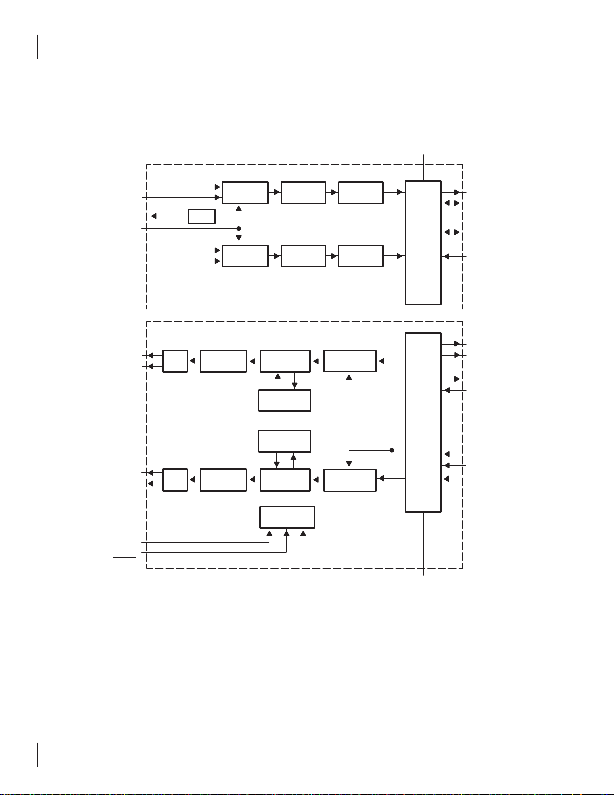
1.2 Functional Block Diagram
INLP
INLM
REFO
REFI
INRP
INRM
L1
L2
R1
R2
VREF
PWM
PWM
Sigma-Delta
Modulator
Sigma-Delta
Modulator
Digital
Modulator
Digital
Modulator
Stereo ADC
Decimation
Filter
Decimation
Filter
Stereo DAC
Interpolation
Filter
De-emphasis
Filter
De-emphasis
Filter
Interpolation
Filter
High-Pass
Filter
High-Pass
Filter
Digital
Attenuator
Digital
Attenuator
3 V or 5 V
V
Serial
Interface
Serial
Interface
35A
ADOUT
SCLKA
LRCKA
MCLKI
256CK
512CK
XOUT
XIN
LRCKD
SCLKD
DDATA
1–2
CDIN
SHIFT
LATCH
CPU
Interface
V
3 V or 5 V
35D
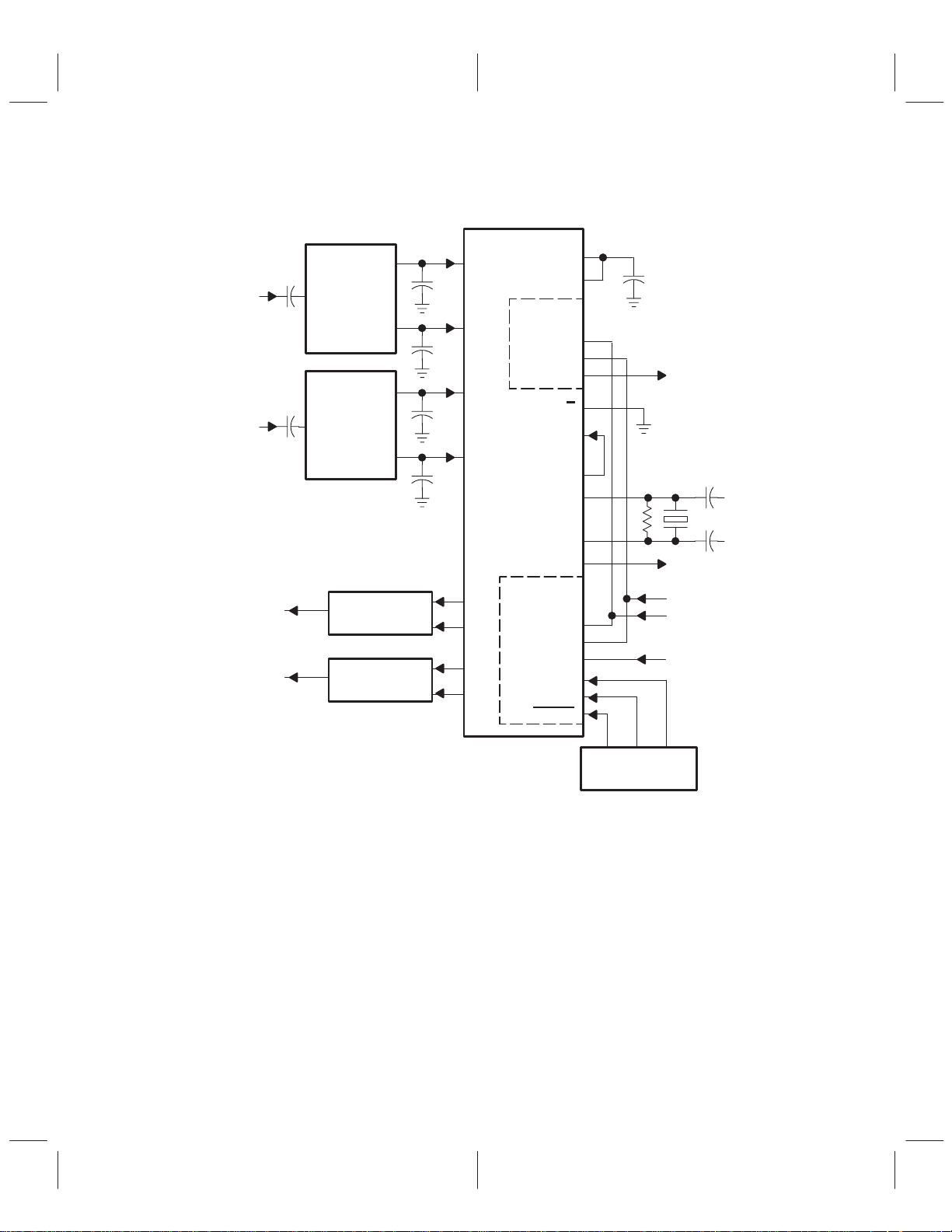
1.3 System Block Diagram
Right
Audio Input
Left
Audio Input
Single to
Differential
Single to
Differential
TLC320AD75C
INRP
ADC
Serial Port
INRM
INLP
INRM
LRCKA
SCLKA
ADOUT
REFI
REFO
M_S
MCLKI
256CK
XIN
AV
SS
ADC Data Out
V
SS1
XV
SS
Audio Output
Right
Left
Audio Output
Analog
Low-Pass Filter
Analog
Low-Pass Filter
R1
R2
L1
L2
XOUT
512CK
DAC
Serial Ports
LRCKD
SCLKD
DDATA
CDIN
SHIFT
LATCH
Microcontroller/
Microprocessor
XV
SCLK
LRCK
DAC Data In
DAC
Control Data
SS
1–3
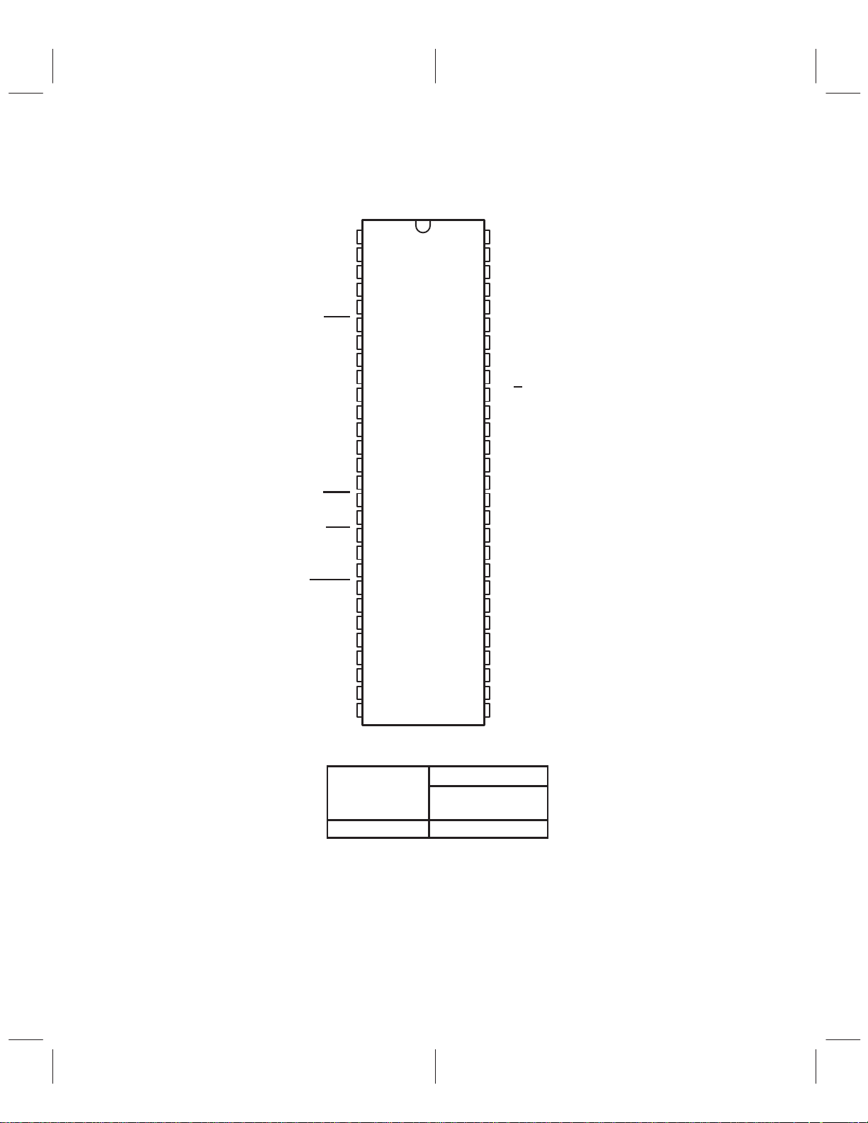
1.4 Terminal Assignments
DL PACKAGE
(TOP VIEW)
INRP
INRM
REFI
AV
DD
AV
SS
APD
NU
NU
TEST1
LRCKA
SCLKA
ADOUT
V
35A
V
SS1B
MCLKI
DPD
V
SS2B
INIT
CDIN
SHIFT
LATCH
256CK
V
35D
V
SS2
512CK
SCLKD
DDATA
LRCKD
1
2
3
4
5
6
7
8
9
10
11
12
13
14
15
16
17
18
19
20
21
22
23
24
25
26
27
28
56
55
54
53
52
51
50
49
48
47
46
45
44
43
42
41
40
39
38
37
36
35
34
33
32
31
30
29
INLP
INLM
REFO
LV
SS
LV
DD
AV
SSB
NU
NU
V
SS1B
M_S
TEST2
V
SS1
V
DD1
V
DD1
V
DD2
L1
PV
DDL
L2
PV
SSL
XV
SS
XIN
XOUT
XV
DD
PV
SSR
R2
PV
DDR
R1
V
DD2
1.5 Ordering Information
1–4
PACKAGE
T
A SMALL OUTLINE
0°C to 70°C TLC320AD75CDL
(DL)
1.6 Terminal Functions
I/O
DESCRIPTION
TERMINAL
NAME NO.
20-bit ADC data output. ADOUT provides the MSB first in 2’s-complement data format
ADOUT 12 O
APD 6 I
AV
DD
AV
SS
AV
SSB
CDIN 19 I
DDATA 27 I
DPD 16 I
INIT 18 I
INLM 55 I Inverting input for the left channel analog modulator
INLP 56 I Noninverting input for the left channel analog modulator
INRM 2 I Inverting input for the right channel analog modulator
INRP 1 I Noninverting input for the right channel analog modulator
LATCH 21 I
LRCKA 10 I/O
LRCKD 28 I
LV
DD
LV
SS
L1 41 O Left channel DAC PWM output 1
L2 39 O Left channel DAC PWM output 2
MCLKI 15 I
4 Analog power supply voltage for ADC modulators
5 Analog ground for ADC modulators
51 Analog substrate ground for ADC modulators
52
53
and is left justified within the 32-bit packet for each channel. The output level is 3.3 V
for V
Analog power-down mode. APD disables the ADC analog modulators. The ADC
single-bit modulator outputs become invalid, rendering the outputs of the digital filters
invalid. When APD
Attenuation mode and system control mode input for DAC. CDIN is a 24-bit stream
with a 16-bit data word followed by an 8-bit device address. This stream is configured
with the MSB first (see Section 2.15,
DAC input data in 2’s-complement data format. MSB/LSB first and 20-bit/16-bit input
formats are selectable by using the DAC control registers (see Section 2.15,
Sigma-Delta DAC Modulator
Digital power-down mode. The DPD shuts down the ADC digital decimation filters and
clock generators, and provides a digital reset. All digital outputs of the ADC function,
are brought to unasserted states. When DPD
device is resumed. When in slave mode operation, after the rising edge of DPD
ADC system is synchronized.
Initial DAC reset signal. The DAC device is activated on the rising edge of INIT . When
INIT
Latch signal for the DAC control serial data. Attenuation/system-control data loads
into the internal registers when LATCH
Left/right clock for ADC. LRCKA signifies whether the serial data is associated with
the left channel ADC (when LRCKA is high) or the right channel ADC (when LRCKA
is low). LRCKA is normally connected to LRCKD. LRCKA is output when configured
in master mode.
Left/right clock for DAC. LRCKD signifies whether the serial data is associated with
the left channel DAC (when LRCKD is high) or the right channel DAC (when LRCKD
is low). LRCKD is normally connected to LRCKA.
Digital power supply for analog modulators. LVDD is normally connected to AV
through a 50-Ω resistor.
Digital ground for analog modulators. L VSS is normally connected to AVSS through a
50-Ω resistor.
Master clock input for ADC. MCLKI operates at 256 times the sample rate (i.e. 256
times LRCKA). MCLKI is normally connected to 256CK through a 50-Ω resistor.
= 3.3 V (see Figure 2–6).
35A
is pulled high, normal operation of the device is resumed.
Sigma-Delta DAC Modulator
).
is pulled high, normal operation of the
is brought low, the DAC is reset when LRCKD is present.
is brought low.
).
, the
DD
1–5
Terminal Functions (Continued)
I/O
DESCRIPTION
TERMINAL
NAME NO.
M_S
NU
PV
DDL
PV
DDR
PV
SSL
PV
SSR
REFI 3 I
REFO 54 O Internal ADC reference voltage (normally connected to REFI).
R1 30 O Right channel DAC PWM output 1
R2 32 O Right channel DAC PWM output 2
SCLKA 11 I/O
SCLKD 26 I
SHIFT 20 I
TEST1 9 I Factory test terminal1. TEST1 should be connected to V
TEST2 46 I Factory test terminal2. TEST2 should be connected to V
XIN 36 I
XOUT 35 O Oscillator output terminal for 512 times the DAC sample rate
V
DD1
V
DD2
V
SS1
V
SS1B
V
SS2
V
SS2B
V
35A
V
35D
XV
DD
XV
SS
256CK 22 O
512CK 25 O
47
7, 8,
49, 50
40 PWM power supply for left channel DAC
31 PWM power supply for right channel DAC
38 PWM ground for left channel DAC
33 PWM ground for right channel DAC
43, 44 Digital power supply for ADC
29, 42 Digital power supply voltage for DAC
45 Digital ground for ADC digital flters
14, 48 Digital substrate ground for ADC
24 Digital ground for the DAC
17 Digital sustrate ground for DAC
13 Digital power supply for ADC interface logic. V
23 Digital power supply for DAC interface logic. V
34 Oscillator power-supply voltage for DAC
37 Oscillator circuit ground for DAC
Master/slave selection. The ADC serial port is configured as master mode when M_S
I
is pulled high. M_S is connected to V
– Not used
Input reference voltage. REFI provides reference voltage for the ADC modulator
(normally connected to REFO).
Shift clock for the ADC. The shift clock clocks serial data out of the ADC, and operates
at 64 times the sample rate (i.e. 64 times LRCKA). SCLKA is normally connected to
SCLKD. SCLKA is output when configured in master mode.
Shift clock for the DAC. The shift clock clocks serial audio data into the DAC, and
operates at 64 times the sample rate (i.e. 64 times LRCKD). SCLKD is normally
connected to SCLKA.
Shift data. SHIFT clocks the control data (CDIN) into the internal control registers for
the DAC.
Oscillator input terminal for 512 times the DAC sample rate. XIN derives all of the key
logic signals of the DAC device. (XIN can also be driven by an external oscillator.)
256 times sample rate clock output. 256CK is normally connected to MCLKI through
a 50-Ω resistor. 256CK is the XIN frequency divided by two.
512 times sample rate clock output (output level is 3.3 V for V
a buffered version of XIN (master clock input).
for slave mode.
SS1
35A
35D
SS1
SS1
is connected to 3 V or 5 V.
is connected to 3 V or 5 V.
for normal operation.
for normal operation.
= 3.3 V). 512CK is
35D
1–6

2 Detailed Description
The sigma-delta ADC converter consists of an oversampling analog modulator and digital decimation filter.
The sigma-delta DAC incorporates an interpolation finite impulse-response (FIR) filter and oversampled
modulator. The pulse-width-modulation (PWM) digital output feeds an external low-pass filter to recover the
analog audio signal.
Two control registers configure the DAC. The attenuation register controls the attenuation range,
de-emphasis enable, and mute selection. The system register controls the data format and de-emphasis
filter-sample rate.
2.1 Power-Down and Reset Functions
2.1.1 ADC Power Down
The power-down state is comprised of a separate digital and analog power down for the ADC. The power
consumption of each is detailed in the electrical characteristics section.
The digital power-down mode shuts down the digital filters and clock generators. When the digital
power-down terminal is pulled high, normal operation of the device is initiated. In slave mode, the conversion
process must synchronize to an input on LRCKA as well as SCLKA. Therefore, the conversion process is
not initiated until the first rising edges of both SCLKA and LRCKA are detected after DPD is pulled high. This
synchronizes the conversion cycle; all conversions are performed at a fixed LRCKA rate after the initial
synchronization. After DPD
cycles which consists of group delays of the decimation and high-pass filter.
The analog power-down mode disables the analog modulators. The single-bit modulator outputs become
invalid, which renders the outputs of the digital filters invalid. When the APD
modulators are brought back online; however, the settling time of the modulator stage is normally 100 ms.
is brought high, the output of the digital filters remains invalid for 26 LRCKA
terminal is brought high, the
2.1.2 Reset Function for ADC
The conversion process is not initiated until the first rising edges of both SCLKA and LRCKA are detected
after DPD
LRCKA rate after the initial synchronization.
is pulled high. This synchronizes the conversion cycle; all conversions are performed at a fixed
2–1
During general operation of the ADC, APD is recommended to be pulled high (APD is not needed for a reset).
When using the analog power-down mode (APD low), the following timing procedure is required to start all
of the ADC since the analog modulator portion which includes the external portion needs to be settled after
is high.
APD
APD
> 100 msec
DPD
LRCKA
> 26 f
ADOUT
s
Figure 2–1. ADC Start-Up Timing
2.1.3 Reset/Initialization for DAC
When INIT is brought low, an internal reset signal becomes active approximately 120 cycles of the sampling
frequency (fs) after the falling edge of INIT. Under this condition, all internal circuits are initialized and the
PWM output is held at zero data (50% duty cycle). When INIT
inactive for a maximum of five LRCKD periods after the rising edge of INIT . At this point, internal clocks are
synchronous with LRCKD and the PWM output is valid (see Figure 2–2). LRCKD must be applied for proper
initialization.
INIT
120 Cycles of f
s
is brought high, the internal reset signal goes
5 periods max
Internal
Reset
LRCKD
2–2
Figure 2–2. DAC-Reset Timing Relationships

2.2 Differential Input to the ADC
The input to the ADC is differential in order to provide common-mode noise rejection and increase the input
dynamic range. Figure 2–3 shows the analog input signals used in a differential configuration to achieve a
6.4 V
differential swing with a 3.2 V
I(PP)
4.1 V
swing per input line.
I(PP)
TLC320AD75C
2.5 V
0.9 V
4.1 V
2.5 V
0.9 V
INLP, INRP
INLM, INRM
Figure 2–3. Differential Analog-Input Configuration
2.3 Sigma-Delta Modulator for the ADC
The modulator is a fourth-order sigma-delta modulator with 64 times oversampling. The ADC provides
high-resolution, low-noise performance from a 1-bit converter using oversampling techniques.
2.4 Decimation Filter
The decimation filter after the sigma-delta ADC modulator reduces the digital data rate to the sampling rate
of LRCKA. This is accomplished by decimating with a ratio of 1:64.
2.5 High-Pass Filter
The high-pass filter removes dc from the input of the ADC. The output of this filter is a 2’s-complement data
word of 20 bits serially clocked out. If the input value exceeds the full range of the converter, the output of
the high-pass filter is held at the appropriate extreme until the input returns to the analog input range of the
TLC320AD75C.
2–3

2.6 Master Clock
2.6.1 Master-Clock Circuit for ADC
The master-clock circuit generates and distributes necessary clocks throughout the device. MCLKI is the
external master-clock input. The sample rate of the data paths is set as LRCKA = MCLKI/256. With a fixed
oversampling ratio of 64 × f
When the TLC320AD75C is in master mode (M_S is pulled high) SCLKA is derived from MCLKI in order
to provide clocking of the serial communications between the sigma-delta audio ADC and a digital signal
processor (DSP) or control logic. This is equivalent to a clock running at 64 × LRCKA.
, the effect of changing MCLKI is shown in Table 2–1.
s
Table 2–1. ADC Master Clock to Sample-Rate Comparison
MCLKI
(MHz)
12.2880 3.0720 48
11.2896 2.8224 44.1
8.1920 2.0480 32
SCLKA
(MHz)
LRCKA
(kHz)
When the TLC320AD75C is in slave mode (M_S
is connected to V
), SCLKA is externally derived. For
SS1
SCLKA use of a clock running at 64 times LRCKA is recommended.
2.6.2 Master-Clock Circuit for DAC
The timing and control circuit generates and distributes necessary clocks throughout the TLC320AD75C.
XIN is the oscillator input terminal or can receive an external master-clock input. The sample rate of the data
paths is set as LRCKD = XIN/512. With a fixed oversampling ratio of 32× and each PWM output value
requiring 16 XIN cycles, the effect of changing XIN is shown in Table 2–2.
Table 2–2. DAC Master Clock to Sample-Rate Comparison
XIN
(MHz)
24.5760 12.2880 48.0
22.5792 11.2896 44.1
16.3840 8.1920 32.0
The DAC can be operated at any conversion rate between 48 kHz and 32 kHz by choosing the appropriate
master-clock frequency. Some of the functions of the converter , such as the deemphasis filter , operate only
at the frequencies shown in Table 2–2.
256CK
(MHz)
LRCKD
(kHz)
2–4

2.7 Test
TEST1 and TEST2 are reserved for factory test and are tied to digital ground (V
SS1
).
2.8 Master Mode for ADC
Configured as the master device (M_S is connected to V
SCLKA from MCLKI. These signals are provided for synchronizing the serial port of a digital signal processor
(DSP) or other control devices.
LRCKA is generated internally from MCLKI. The frequency of LRCKA is fixed at the sampling frequency,
(MCLKI/256). During the high period of LRCKA, the left channel data is serially shifted to the output; during
f
s
the low period, the right channel data is shifted to the output (ADOUT). The conversion cycle is synchronized
with the rising edge of LRCKA.
Figure 2–4 (master mode) shows 20-bit data, MSB first, ADOUT data shifted out of the TLC320AD75 during
the first 20 SCLKA periods of the 32 SCLKA periods for both left and right channel data.
20-BIT MASTER MODE
LSB
SCLKA
ADOUT
LRCKA
Output
Output
Output
MSB
19 18 . . . 1 0 19 18 . . . 1 0
Left
Figure 2–4. ADC Audio-Data Serial Timing – Master Mode
), the TLC320AD75C generates LRCKA and
DD1
MSB
64 SCLKs
Right
LSB
MSB
19
18
2.9 Slave Mode for ADC
Configured as a slave device (M_S is connected to V
as inputs. The conversion cycle is synchronized to the rising edge of LRCKA, and the data is synchronized
to the falling edge of SCLKA. SCLKA must meet the setup requirements specified in the recommended
operating conditions section. Synchronization of the slave mode is accomplished with the rising edge of
.
DPD
), the TLC320AD75C receives LRCKA and SCLKA
SS1
The slave mode is shown in Figure 2–5. SCLKA and LRCKA are externally generated and sourced. The
first rising edges of SCLKA and LRCKA after the rising edge of DPD
Section 2.8,
Master Mode for ADC
for signal functions).
initiate the conversion cycle (see
Figure 2–5 (slave mode) shows 20-bit data, MSB first, and ADOUT data shifted out of the TLC320AD75
during the first 20 SCLKA periods of the 32 SCLKA periods for both left and right channel data.
20-BIT SLAVE MODE
. . .
LSB
10
64 SCLKs
MSB
19 18
Right
. . .
LSB
10
SCLKA
ADOUT
LRCKA
input
output
input
MSB
19 18
Left
Figure 2–5. ADC Audio-Data Serial Timing – Slave Mode
2.10 Digital-Audio Data Interface for DAC
The conversion cycle is synchronized to the rising edge of LRCKD, and the data must meet the setup
requirements specified in the timing requirements table. The input data is 16 or 20 bits with the MSB or LSB
first as selected in the system register. The recommended SCLKD frequency is 64 × f
illustrates the input timing.
. Figure 2–6
s
2–5

2–6
LRCKA and LRCKD
SCLKA and SCLKD
ADOUT
DDOUT
(20-Bit, MSB First)
DDOUT
(16-Bit, MSB First)
DDOUT
(20-Bit, LSB First)
DDOUT
(16-Bit, LSB First)
LEFT RIGHT
1 32 64
MSB LSB MSB LSB
MSB LSB MSB LSB
MSB LSB MSB LSB
LSB MSB LSB MSB
LSB MSB LSB MSB
Figure 2–6. Audio-Data Serial Timing – ADC and All DAC Modes

2.11 Serial-Control Interface for DAC
The TLC320AD75C uses the most-significant-bit-first format. Therefore, for a 16-bit data word, D16 is the
most significant bit (MSB) and D1 is the least significant bit (LSB).
2.11.1 Serial-Control-Data Input
The 16-bit control-data input implements the device-control functions. The TLC320AD75C has two registers
for this data: the system register and the attenuation register. The system register contains most of the
system configuration information, and the attenuation register controls the audio output level and
deemphasis. Figure 2–7 illustrates the input timing for CDIN, SHIFT , and LATCH
during the low level of LA TCH. The shift clock must be high or low for the LA TCH setup time before LA TCH
goes low.
As shown in Figure 2–7, CDIN is a 24-bit data stream consisting of 16 bits of control data D16 through D1
followed by 8 bits of device, address A8 through A1. When the TLC320AD75C receives address >E7h, the
control data is latched into the device by LA TCH. For all other addresses, the data is ignored.
Control Data Control-Device Address
. The data loads internally
CDIN
SHIFT
LATCH
D16 D15
D13 D12 D11 D10 D9 D8 D7
D14
D6 D5 D4 D3 D2 D1 A8 A7 A6 A5 A4 A3 A2 A1
Figure 2–7. Control-Data Input Timing
2.12 DAC De-emphasis Filter
Three sets of de-emphasis-filter coefficients support the three sampling rates (fs): 32 kHz, 44.1 kHz, and
48 kHz. Internal system-register values select the filter coefficients. The internal register values enable or
disable the filter. Figure 2–8 illustrates the de-emphasis filtering characteristics.
Many audio sources have been recorded with pre-emphasis characteristics that are the inverse of the
characteristics shown in Figure 2–8. This device provides reconstruction of the original frequency response.
10
0
Response – dB
De-emphasis
–10
3.18
(50 µs)
f – Frequency – kHz
10.6
(15 µs)
Figure 2–8. De-emphasis Filter Characteristics
2.13 Digital Filter Mute for DAC
When the mute bit in the attenuation register is set to 1, the DAC digital filter mute is active. The output of
the digital filter is 0 + dc offset. Operation of the digital filter is normal during mute.
2–7

2.14 DAC Digital Attenuation/Soft Mute
A value selected in the internal attenuation register determines the attenuation of the digital-audio data input.
The attenuation value is 12 bits long with a valid range of hex values from 400h to 000h. A data value of 001h
corresponds to an attenuation value of – 60 dB and a data value of 400h corresponds to 0 dB. The
attenuation function is nonlinear. Figure 2–9 illustrates the attenuation function in dB. The default
attenuation value is 400h (refer to the attenuator mode register for more detailed description).
attenuation data
Attenuation+20 log
0
–10
–20
–30
Attenuation – dB
–40
–50
ǒ
1024
Ǔ
–60
1024 896 768 640 512 384 256 128 0
Attenuation Data (decimal values)
Figure 2–9. Digital Attenuation Characteristics
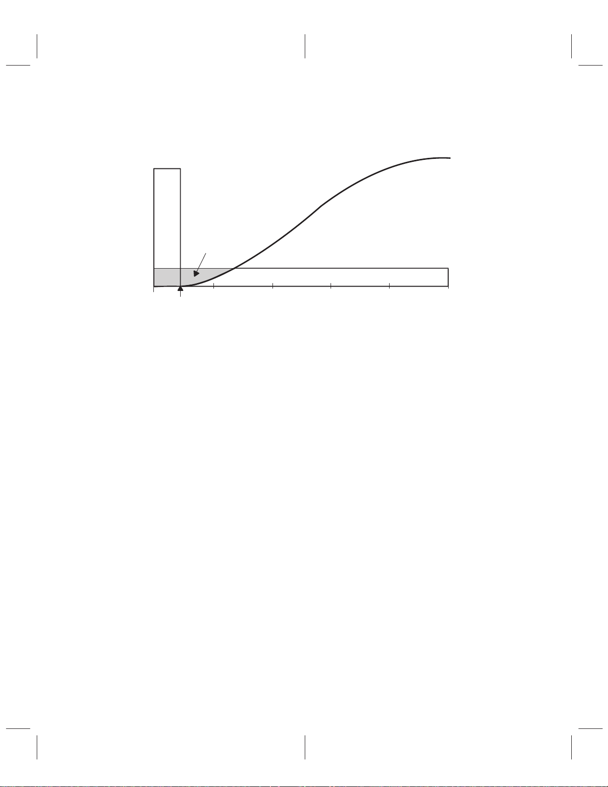
The attenuation operation of the DAC has a tapered gain response. It takes time T = 1024/f
(sec) to reach
s
the actual 000H data output after an A TT = 000H data transfer from 400H data as shown in Figure 2–10.
400H
200H
Output Level (ATT)
000H
T T
ATT = 000H
Transfer
ATT = 400H
Transfer
T = 1024/fs (sec)(Soft Mute)
Figure 2–10. DAC Digital Attenuation Operation with Tapered Gain Response
2–8
2.15 Sigma-Delta DAC Modulator
The DAC uses a third-order modulator with 32 times oversampling. The DAC provides high-resolution,
low-noise performance using a 15-value PWM output as shown in Figure 2–1 1.
A
†
PB(max)
Audio
Signal
Noise Excluded by
Noise Power – dB
0
0 0.1 0.2 0.3 0.4 0.5
†
A
PB(max)
‡
fB is the highest frequency of interest within the baseband.
§
fO is the output frequency at the external low-pass filter output.
Low-Pass Filter
Quantization Noise Power Without Noise Shaping
‡
f
B
is the passband maximum amplitude.
Normalized Analog-Output Frequency (fO/f
Quantization Noise Power With Noise Shaping
§
)
s
Figure 2–11. Oversampling Noise Power With and Without Noise Shaping
2.16 DAC Interpolation Filter
The interpolation filter used prior to the DAC increases the digital-data rate from the LRCKD speed to the
oversampled rate by interpolating with a ratio of 1:32. The oversampling modulator receives the output of
this filter with de-emphasis as an option.
2.17 DAC PWM Output (L2–L1 and R2–R1)
The L2 – L1 and the R2– R1 output pairs are PWM signals with the L2 – L1 differential pulse duration
determining the left-channel analog voltage and the R2 – R1 differential pulse duration determining the
right-channel analog voltage.
Each DAC left and right output consists of 15 levels of PWM and provides a differential signal as the input
to two external differential amplifiers configured as a low-pass filter to produce the left and right audio
outputs.
2–9

2.18 DAC Control Register Set
(D5 = MSB
D16 = LSB)
D/F mute
De-emphasis enable
DAC register select
DAC mode
Tables 2–3 and 2–4 list the bit functions.
T able 2–3. Attenuation Mode Register
D16–D5
0h - - - - Muted
1h - - - - Digital attenuation, –60.2 dB
2h - - - - Digital attenuation, –54.2 dB
3h - - - - Digital attenuation, –50.7 dB
D4 D3 D2 D1 DESCRIPTION
†
1FFh - - - 200h - - - 201h - - - - Digital attenuation, –6.02 dB
3FFh - - - - Digital attenuation, –0.01 dB
400h - - - - Digital attenuation, 0 dB
- 0 - - -
- 1 - - -
- - 0 - -
- - 1 - -
- - - 0 -
- - - 1 -
- - - - 0
- - - - 1
†
The initialization value is 0400h.
DAC attenuation
,
=
p
=
Digital attenuation, –6.04 dB
Digital attenuation, –6.02 dB
Unmuted
Muted
No de-emphasis
De-emphasis selected
Attenuator-mode register
System-mode register
Normal
Factory test only
2–10

T able 2–4. System Mode Register
Resynchronize
d
Input-data word width
Input D-data protocol
DAC register select
DAC mode
D16
D15 D14 D13 D12–D5 D4 D3 D2 D1 DESCRIPTION
0 - - - - - - - - Reserved
- 0 - - - - - - -
- 1 - - - - - - -
- - 0 0 - - - - - 44.1 kHz
- - 0 1 - - - - -
- - 1 0 - - - - -
- - 1 1 - - - - - 32 kHz
- - - - 0 - - - - Reserved
- - - - - 0 - - -
- - - - - 1 - - -
- - - - - - 0 - -
- - - - - - 1 - -
- - - - - - - 0 -
- - - - - - 1 -
- - - - - - - - 0
- - - - - - - - 1
†
The initialization value is 0000h.
Sample rate/
e-emphasis
selection
p
p
DAC register select
†
Off
On
p
p
Reserved
48 kHz
20 bits audio data
16 bits audio data
MSB first
LSB first
Attenuator-mode
register
System-mode register
Normal
Factory test only
2.19 Auto-Resynchronization Functionality
The TLC320AD75C has an auto-resynchronization function to keep the entire coversion cycle for the ADC
portion and DAC portion respectively checking the LRCK cycle of the fs rate. When the ADC is in slave mode,
the ADC portion has a window of "4 clocks of the internal 64 f
rate detecting the rising edge of LRCK within this window. When an error is detected on the LRCK cycle,
the ADC conversion cycle is resynchronized with an external LRCK cycle at the next rising edge of LRCK.
This resynchronization occurrs automatically and the ADC portion continues processing based on the new
conversion cycle timing.
The DAC portion has a window of "2 clocks of the internal 128 fs clock to check the LRCK cycle detecting
the rising edge of the LRCK clock. When an error is detected, the conversion cycle of the DAC is
resynchronized with an external LRCK cycle automatically and the DAC portion continues processing based
on the new conversion cycle timing. (The external LRCK rate should be the same as the fs rate. This
functionality is to ensure the TLC320AD75C conversion operation even if LRCK has a timing problem due
to noise injection for example.)
clock to check the LRCK cycle with the f
s
s
2–11

2–12

3 Specifications
3.1 Absolute Maximum Ratings Over Operating Free-Air Temperature Range
(unless otherwise noted)
†
Supply voltage range, AV
Supply voltage range, V
Supply voltage range, PV
Analog input voltage range, INLP, INLM, INRP, INRM –0.3 V to A V
Digital input voltage range –0.3 V to V
Output voltage range, V
Operating free-air temperature range, T
Storage temperature range, T
, LVDD (see Note 1) –0.3 V to 6.5 V. . . . . . . . . . . . . . . . . . .
DD
, V
DD1
DD(L/R)
: L1, L2, R1, R2 –0.3 V to A VDD + 0.3 V. . . . . . . . . . . . . . . . .
O
(see Note 2) –0.3 V to 6.5 V. . . . . . . . . . . . . . . . . . . .
35A
, V
, V
DD2
, XVDD(see Note 3) –0.3 V to 6.5 V. . . .
35D
A
stg
–65°C to 150°C. . . . . . . . . . . . . . . . . . . . . . . . . . . . . . . .
DD
DD1/2
–0°C to 70°C. . . . . . . . . . . . . . . . . . . . . . . . . . .
+ 0.3 V. . . . . . .
+ 0.3 V. . . . . . . . . . . . . . . . . . . . . . . . . . . . .
Case temperature for 10 seconds 260°C. . . . . . . . . . . . . . . . . . . . . . . . . . . . . . . . . . . . . . . .
Lead temperature 1,6 mm (1/16 inch) from case for 10 seconds 260°C. . . . . . . . . . . . . .
†
Stresses beyond those listed under “absolute maximum ratings” may cause permanent damage to the device. These
are stress ratings only, and functional operation of the device at these or any other conditions beyond those indicated
under “recommended operating conditions” is not implied. Exposure to absolute-maximum-rated conditions for
extended periods may affect device reliability.
NOTES: 1. Voltage values for maximum ratings are with respect to AVSS.
2. Voltage values for maximum ratings are with respect to V
3. Voltage values for maximum ratings are with respect to V
SS1
SS2
.
.
3.2 Recommended Operating Conditions
MIN NOM MAX UNIT
Analog supply voltage, A VDD (see Note 4) 4.75 5 5.25 V
Digital supply voltage, V
Analog logic supply voltage, LV
Reference voltage at REFI 3.2 V
Digital supply voltage, V
Digital supply voltage, V
Digital supply voltage, PV
Clock supply voltage, XV
Setup time, SCLKA/SCLKD↑ before LRCKA/LRCKD valid, t
Setup time, LRCKA/LRCKD valid before SCLKA/SCLKD↑, t
Load resistance at ADOUT, R
Operating free-air temperature, T
NOTE 4: Voltages at analog inputs and outputs and A VDD are with respect to AVSS.
DD1
35A
DD2
DDL
DD
, V
DD
35D
, PV
L
A
DDR
(see Figure 4–2) 50 ns
su1
(see Figure 4–2) 50 ns
su2
4.75 5 5.25 V
4.75 5 5.25 V
3 3.3 5.25 V
4.75 5 5.25 V
4.75 5 5.25 V
4.75 5 5.25 V
8 kΩ
0 70 °C
3–1

3.3 Electrical Characteristics, AVDD = LVDD = V
V
Analog input voltage, ADC
= XV
3.3.1 Digital Interface
DD
= 5 V, V
35A
= V
= 3.3 V, TA = 25°C
35D
DD1
= V
DD2
= PV
DDL
= PV
DDR
PARAMETER TEST CONDITIONS MIN TYP MAX
V
High-level input voltage 2 3.3 V
IH
V
High-level input voltage XIN 4.5 5 V
IH
V
Low-level input voltage 0.2 0.8 V
IL
V
Low-level input voltage XIN 0.2 0.8 V
IL
V
High-level output voltage
OH
V
Low-level output voltage
OL
I
High-level input current, any digital input 0.1 µA
IH
I
Low-level input current, any digital input 0.1 µA
IL
C
Input capacitance 5 pF
i
C
Output capacitance 5 pF
o
3.3.2 Analog Interface
PARAMETER TEST CONDITIONS MIN TYP MAX
I(analog)
Z
i
Input impedance, ADC 200 kΩ
p
ADOUT IOH = 0.4 mA 2.6 3.2
512CK
256CK
L1, L2, R1, R2 IOH = 0.4 mA 4.5 4.9
XOUT IOH = 1.2 mA 4.5 4.9
ADOUT IOL = 2 mA 0.2 0.4
512CK IOL = 2 mA 0.2 0.4
256CK
L1, L2, R1, R2 IOL = 2 mA 0.2 0.5
XOUT IOL = 1.2 mA 0.2 0.5
IOH = 0.4 mA 2.6 3.2
IOH = 0.4 mA 4.5 4.9
IOL = 2 mA 0.2 0.4
Differential 6.4 V
0 to peak 3.2 V
UNIT
V
V
UNIT
3–2

3.3.3 ADC Performance, fs = 44.1 kHz, Bandwidth = 22.05 kHz
input
Absolute gain error
De-emphasis
Input voltage range
V
PARAMETER TEST CONDITIONS MIN TYP MAX
Resolution 20 Bits
DYNAMIC PERFORMANCE
Signal to noise (EIAJ)
Dynamic range – 60 dB input 100 dB
Signal to noise + distortion (THD + N)
Total harmonic distortion (THD)
Interchannel isolation 120 dB
DC ACCURACY
Interchannel gain mismatch ±0.2 dB
Offset drift 0 LSB/°C
INLP = INRP = 2.5 V dc
INLM = INRM = 2.5 V dc
– 0.5 dB
– 0.5 dB IN ±0.2 ±0.5 dB
p
96 100 dB
0.0017% 0.003%
0.001%
±0.2 dB
UNIT
3.3.4 DAC Performance, 20-Bit Mode, fs = 44.1 kHz, Bandwidth = 22.05 kHz
PARAMETER TEST CONDITIONS MIN TYP MAX UNIT
Resolution See Note 5 20 bits
Signal-to-noise ratio
Signal-to-noise + distortion
(THD + N)
NOTE 5: These specifications are measured at the output (VO) of the external low-pass filter.
See Note 5
See Note 5
p
not selected
100 104 dB
0.0013% 0.0025%
3.3.5 ADC Inputs
PARAMETER TEST CONDITIONS MIN TYP MAX
ANALOG INPUT
p
Input impedance 200 kΩ
Differential 6.4
0 to peak 3.2
3.3.6 ADC High-Pass Filter, fs = 44.1 kHz
PARAMETER TEST CONDITIONS MIN TYP MAX UNIT
Passband (–3 dB) 0.86 Hz
Passband 5 Hz –0.12 dB
Group delay 1/f
s
3.3.7 ADC Decimation Filter, fs = 44.1 kHz
PARAMETER TEST CONDITIONS MIN TYP MAX
Passband ripple 20.03 kHz ±0.01 dB
Stopband attenuation 24.07 kHz 80 dB
Group delay 25/f
s
UNIT
s
UNIT
s
3–3

3.3.8 DAC Filter Characteristics, fs = 44.1 kHz
PSRR
Power-supply rejection ratio
PARAMETER TEST CONDITIONS MIN TYP MAX UNIT
Pass-band ripple fs = 20 kHz ±0.002 dB
Stop-band attenuation fs = 24.1 kHz 75 dB
Group delay 29/f
s
3.3.9 Power Supply Current, fs = 44.1 kHz
s
I
DD(A)
I
DD(AD)
I
DD(DA1)
I
DD(DA2)
I
DD(AST)
I
DD(DST)
P
D
PARAMETER
Power-supply current,
analog (ADC)
Power-supply current,
digital (ADC)
Power-supply current,
digital (DAC)
Power-supply current,
PWM/OSC (DAC)
Power-down current,
analog (ADC)
Power-down current,
digital (ADC)
Power dissipation 400 mW
pp
AVDD and LV
VDD1 and V35A 22 30 mA
VDD2 and V35D 20 25 mA
PVDDL, PVDDR,
and XVDD
AVDD and LVDD 250 µA
VDD1 and V35A 150 µA
TEST CONDITIONS MIN TYP MAX UNIT
DD
0 to 24 kHz 75 dB
24 kHz to 2.798 MHz 85 dB
3.4 ADC Switching Characteristics (see Figures 2–1 and 4–1)
PARAMETER MIN TYP MAX
f
MCKI
t
d(MDD)
t
d(MIRD)
t
d(SDD1)
t
d(SDD2)
Input clock frequency , MCKI 11.3 12.8 MHz
Delay time, SCLKA↓ to ADOUT, master mode 0 50 ns
Delay time, SCLKA↓ to LRCKA, master mode –20 20 ns
Delay time, LRCKA to ADOUT, slave mode 50 ns
Delay time, SCLKA↓ to ADOUT, slave mode 50 ns
29 40 mA
17 25 mA
UNIT
3–4

3.5 DAC Timing Requirements (see Figures 4–1 and 4–2, and Note 6)
MIN TYP MAX UNIT
f
t
t
t
t
t
t
t
t
t
NOTE 6: All timing measurements were taken at the VDD/2 voltage level.
Input frequency, XIN clock 22.6 25.6 MHz
XIN
Pulse duration, SCLKD 155 177 ns
w1
Pulse duration, SHIFT 100 ns
w2
Pulse duration, LATCH 100 ns
w3
Setup time, DDATA valid before SCLKD↑ 20 ns
su3
Hold time, DDATA valid after SCLKD↑ 20 ns
h1
Setup time, CDIN valid before SHIFT↑ 20 ns
su4
Hold time, CDIN valid after SHIFT↑ 20 ns
h2
Setup time, LATCH↑ before SHIFT↑ 100 ns
su5
Hold time, LATCH↓ after SHIFT↑ 80 ns
h3
3–5

3–6

4 Parameter Measurement Information
SRCKA/
SRCKD
LRCKA/
LRCKD
ADOUT
DDATA
SHIFT
CDIN
t
su3
t
su1
t
d(sdd1)
t
h1
t
su2
t
d(MIRD)
Figure 4–1. ADC Audio-Data Serial Timing
t
w2
t
su4
t
w2
t
h2
t
w1
t
d(sdd2), td(MDD)
t
h3
t
su5
t
w1
LATCH
t
w3
Figure 4–2. DAC Control-Data Serial Timing
4–1

4–2

5 Application Information
T able 5–1. TLC320AD75C Schematic Components
SYMBOL DESCRIPTION
C1 220-µF capacitor
C2 4700-pF capacitor
C3 4700-pF capacitor
C4 220-µF capacitor
C5 47-µF capacitor
C6 22-µF capacitor
C7 0.1-µF capacitor
C8 100-µF capacitor
C9 0.1-µF capacitor
C10 220-µF capacitor
C12 220-µF capacitor
C13 18-pF capacitor
C14 12-pF capacitor
C15 220-µF capacitor
C16 47-µF capacitor
C17 0.1-µF capacitor
C18 4700-µF capacitor
C19 4700-µF capacitor
C20 200-pF capacitor
C21 100-µF capacitor
C22 0.1-µF capacitor
C23 200-pF capacitor
C24 100-pF capacitor
C25 47-µF capacitor
C26 22-µF capacitor
C27 220-µF capacitor
C28 220-µF capacitor
C29 47-µF capacitor
C30 100-pF capacitor
C31 47-µF capacitor
C32 30-pF capacitor
C33 120-pF capacitor
C34 30-pF capacitor
C35 30-pF capacitor
C36 120-pF capacitor
5–1

T able 5–1. TLC320AD75C Schematic Components (Continued)
SYMBOL DESCRIPTION
C37 30-pF capacitor
C38 100-µF capacitor
C39 100-µF capacitor
C40 4700-pF capacitor
C41 1200-pF capacitor
C42 1200-pF capacitor
C43 4700-pF capacitor
C44 47-µF capacitor
C45 47-µF capacitor
C46 100-µF capacitor
C47 100-µF capacitor
C48 47-µF capacitor
C49 47-µF capacitor
C50 0.1-µF capacitor
C51 0.1-µF capacitor
C52 0.1-µF capacitor
C53 47-µF capacitor
C54 220-µF capacitor
C55 0.1-µF capacitor
R1 50-Ω resistor
R2 50-Ω resistor
R3 50-Ω resistor
R4 50-Ω resistor
R5 50-Ω resistor
R6 50-Ω resistor
R7 50-Ω resistor
R8 50-Ω resistor
R9 50-Ω resistor
R10 50-Ω resistor
R11 50-Ω resistor
R12 50-Ω resistor
R13 50-Ω resistor
R14 1-MΩ resistor
R15 50-Ω resistor
R16 50-Ω resistor
R17 50-Ω resistor
R18 5-kΩ resistor
R19 620-Ω resistor
R20 10-kΩ resistor
R21 5-kΩ resistor
5–2

T able 5–1. TLC320AD75C Schematic Components (Continued)
SYMBOL DESCRIPTION
R22 4.7-kΩ resistor
R23 5-kΩ resistor
R24 620-Ω resistor
R25 68-kΩ resistor
R26 33-kΩ resistor
R27 18-kΩ resistor
R28 33-kΩ resistor
R29 18-kΩ resistor
R30 68-kΩ resistor
R31 68-kΩ resistor
R32 33-kΩ resistor
R33 18-kΩ resistor
R34 33-kΩ resistor
R35 18-kΩ resistor
R36 68-kΩ resistor
R37 1.5-kΩ resistor
R38 1.5-kΩ resistor
R39 1.5-kΩ resistor
R40 1.5-kΩ resistor
R41 100-Ω resistor
R42 100-Ω resistor
R43 100-Ω resistor
R44 100-Ω resistor
R45 330-kΩ resistor
R46 330-kΩ resistor
R47 10-kΩ resistor
R48 10-kΩ resistor
R49 10-kΩ resistor
R50 10-kΩ resistor
5–3

LRCK
SCLK
ADOUT
DPD
CDIN
SHIFT
LATCH
512CK
DDAT
AV
V
C53
AV
V35A
SS1B
V35D
V
SS2
DD
SS
DV
DV
DD
SS
INRM
INRP
INLP
INLM
L1
L2
PV
R2
R1
SSR
C2
C1
C5C4
R48
AV
DD
SS
R49
R1
R2
C7C6
R3
AV
SS
R4
R5
R6
R7
R8
C9C8
R9
R10
R11
AV
10
11
12
13
14
15
16
17
18
19
20
21
22
23
24
25
26
27
28
1
2
3
4
5
6
7
8
9
C3
INRP
INRM
REFI
AV
DD
AV
SS
APD
NU
NU
TEST1
LRCKA
SCLKA
ADOUT
V
35A
V
SS1B
MCLKI
DPD
V
SS2B
INIT
CDIN
SHIFT
LATCH
256CK
V
35D
V
SS2
512CK
SCLKD
DDATA
LRCKD
56
INLP
55
INLM
54
REFO
53
LV
SS
52
LV
DD
51
AV
SSB
50
NU
49
NU
48
V
SS1B
47
M_S
46
TEST2
45
V
SS1
44
V
DD1
43
V
DD1
42
V
DD2
PV
PV
PV
PV
DDL
SSL
XV
XIN
XOUT
XV
DD
SSR
DDR
V
DD2
SS
R2
R1
41
L1
40
39
L2
38
37
36
35
34
33
32
31
30
29
TLC320AD75C
R17
R16
C18
R50
C16
C15
C12
C19
C10
R15
AV
C13
R14
C11
SS
AV
AV
C17
R12
SS
DD
V
SS1B
R13
V
V
XTL
SS1
DD1
C14
5–4
C54
C55
AV
Figure 5–1. TLC320AD75C Application Schematic
SS

INRM
INRP
INLP
INLM
C21
C26
R18
C24
R 47
C25
C29
C20
+
AV
DD
C23
R20
TL32088
C27
12345678910
20191817161514131211
C28
R19
R21
R22
AV
AINR
DD
PV
SSR
R2
R1
C30
R23
C31
R24
C32
R30
R31
R25
–
+
C39
+
+
+
–
R36
C37
L1
L2
R26 R27
C33
R28 R29
C34
C35
R32 R33
C36
R34 R35
–15 V
C38
R37
C40
R40R39
C41
C22
+
+
C50
R38
C43
–
+
+
C42
+
–
C47
+
R41
C46
R43
15 V
+
C48 C49
++
C51
C52
+
GND
C44 C45
++
R42
R46
R45
R44
AINL
AOUTL
AOUTR
Figure 5–1. TLC320AD75C Application Schematic (Continued)
5–5

T able 5–2. A-Weighted Data
FREQUENCY A WEIGHTING (dB) FREQUENCY A WEIGHTING (dB)
25 –44.6 ±2 800 –0.1 ±1
31.5 –39.2 ±2 1000 0 ±0
40 –34.5 ±2 1250 0.6 ±1
50 –30.2 ±2 1600 1.0 ±1
63 –26.1 ±2 2000 1.2 ±1
80 –22.3 ±2 2500 1.2 ±1
100 –19.1 ±1 3150 1.2 ±1
125 –16.1 ±1 4000 1.0 ±1
160 –13.2 ±1 5000 0.5 ±1
200 –10.8 ±1 6300 –0.1 ±1
250 –8.6 ±1 8000 –1.1 ±1
315 –6.5 ±1 10000 –2.4 ±1
400 –4.8 ±1 12500 –4.2 ±2
500 –3.2 ±1 16000 –6.5 ±2
630 –1.9 ±1
10
0
–10
–20
Attenuation – dB
–30
–40
–50
20 100 1 k 10 k 20 k
f – Signal Frequency – Hz
Figure 5–2. A-Weighted Function
5–6

5.1 Circuit And Layout Considerations
The designer should follow these guidelines for the best device performance.
• Separate digital and analog ground planes should be used. All digital device functions should be
over the digital ground plane, and all analog device functions should be over the analog ground
plane. The ground planes should be connected at only one point to the direct power supply , and
this is usually at the connector edge of the board.
• A single crystal-controlled clock should synchronously generate all digital signals.
• All power supply lines should include a 0.1-µF and a 1-µF capacitor. When clock noise is
excessive, a toroidal inductance of 10 µH should be placed in series with XV
DD
.
to DV
• The digital input control signals should be buffered when they are generated off of the card.
• Clock jitter should be minimized, and precautions taken to prevent clock overshoot. This
minimizes any high-frequency coupling to the analog output.
before connecting
DD
5.2 PCB Footprint
Figure 5–3 shows the printed-circuit-board (PCB) land pattern for the TLC320AD75C small-outline
package.
W
L1
L
P
L2
L2
L
L1
P
1.27S9.53W0.76L1.55L10.64L20.91
NOTE A: All linear dimensions are in millimeters.
Figure 5–3. Land Pattern for PCB Layout
S
5–7

5–8

Appendix A
Mechanical Data
DL (R-PDSO-G**) PLASTIC SMALL-OUTLINE PACKAGE
48 PIN SHOWN
48
1
0.110 (2,79) MAX
0.025 (0,635)
0.012 (0,305)
0.008 (0,203)
A
0.008 (0,20) MIN
0.005 (0,13)
25
0.299 (7,59)
0.291 (7,39)
24
DIM
M
0.420 (10,67)
0.395 (10,03)
Seating Plane
0.004 (0,10)
PINS **
A MAX
A MIN
0.006 (0,15) NOM
0.380
(9,65)
0.370
(9,40)
Gage Plane
0°–8°
4828
0.630
(16,00)
0.620
(15,75)
56
0.730
(18,54)
0.720
(18,29)
0.010 (0,25)
0.040 (1,02)
0.020 (0,51)
NOTES: A. All linear dimensions are in inches (millimeters).
B. This drawing is subject to change without notice.
C. Body dimensions do not include mold flash or protrusion not to exceed 0.006 (0,15).
4040048/B 02/95
A–1

A–2

IMPORTANT NOTICE
T exas Instruments and its subsidiaries (TI) reserve the right to make changes to their products or to discontinue
any product or service without notice, and advise customers to obtain the latest version of relevant information
to verify, before placing orders, that information being relied on is current and complete. All products are sold
subject to the terms and conditions of sale supplied at the time of order acknowledgement, including those
pertaining to warranty, patent infringement, and limitation of liability.
TI warrants performance of its semiconductor products to the specifications applicable at the time of sale in
accordance with TI’s standard warranty. Testing and other quality control techniques are utilized to the extent
TI deems necessary to support this warranty . Specific testing of all parameters of each device is not necessarily
performed, except those mandated by government requirements.
CERT AIN APPLICATIONS USING SEMICONDUCTOR PRODUCTS MA Y INVOLVE POTENTIAL RISKS OF
DEATH, PERSONAL INJURY, OR SEVERE PROPERTY OR ENVIRONMENTAL DAMAGE (“CRITICAL
APPLICATIONS”). TI SEMICONDUCTOR PRODUCTS ARE NOT DESIGNED, AUTHORIZED, OR
WARRANTED TO BE SUITABLE FOR USE IN LIFE-SUPPORT DEVICES OR SYSTEMS OR OTHER
CRITICAL APPLICA TIONS. INCLUSION OF TI PRODUCTS IN SUCH APPLICATIONS IS UNDERST OOD TO
BE FULLY AT THE CUSTOMER’S RISK.
In order to minimize risks associated with the customer’s applications, adequate design and operating
safeguards must be provided by the customer to minimize inherent or procedural hazards.
TI assumes no liability for applications assistance or customer product design. TI does not warrant or represent
that any license, either express or implied, is granted under any patent right, copyright, mask work right, or other
intellectual property right of TI covering or relating to any combination, machine, or process in which such
semiconductor products or services might be or are used. TI’s publication of information regarding any third
party’s products or services does not constitute TI’s approval, warranty or endorsement thereof.
Copyright 1998, Texas Instruments Incorporated
 Loading...