

查询TL5002供应商
TL5002
PULSE-WIDTH-MODULATION CONTROL CIRCUIT
SLVS304A – SEPTEMBER 2000 – REVISED AUGUST 2002
CC
D PACKAGE
(TOP VIEW)
1
2
3
4
8
7
6
5
GND
RT
DTC
NI
D Complete PWM Power Control
D 3.6-V to 40-V Operation
D Internal Undervoltage-Lockout Circuit
D Oscillator Frequency . . . 20 kHz to 500 kHz
D Variable Dead Time Provides Control Over
Total Range
OUT
V
COMP
INV
D Ideal Controller for DDR Memory
Application
D Uncommitted Error Amplifier Inputs
description
The TL5002 incorporates on a single monolithic chip all the functions required for a pulse-width-modulation
(PWM) control circuit. Designed primarily for power-supply control, the TL5002 contains an error amplifier, a
regulator, an oscillator, a PWM comparator with a dead-time-control input, undervoltage lockout (UVLO), and
an open-collector output transistor.
The error-amplifier input common-mode voltage ranges from 0.9 V to 1.5 V. Dead-time control (DTC) can be
set to provide 0% to 100% dead time by connecting an external resistor between DTC and GND. The oscillator
frequency is set by terminating RT with an external resistor to GND. During low V
turns the output off until V
recovers to its normal operating range.
CC
The TL5002 is characterized for operation from –40°C to 85°C.
AVAILABLE OPTIONS
T
A
–20°C to 85°C TL5002CD
–40°C to 85°C TL5002ID
The D package is available taped and reeled. Add the suffix R
to the device type (e.g., TL5002CDR).
SMALL OUTLINE
(D)
conditions, the UVLO circuit
CC
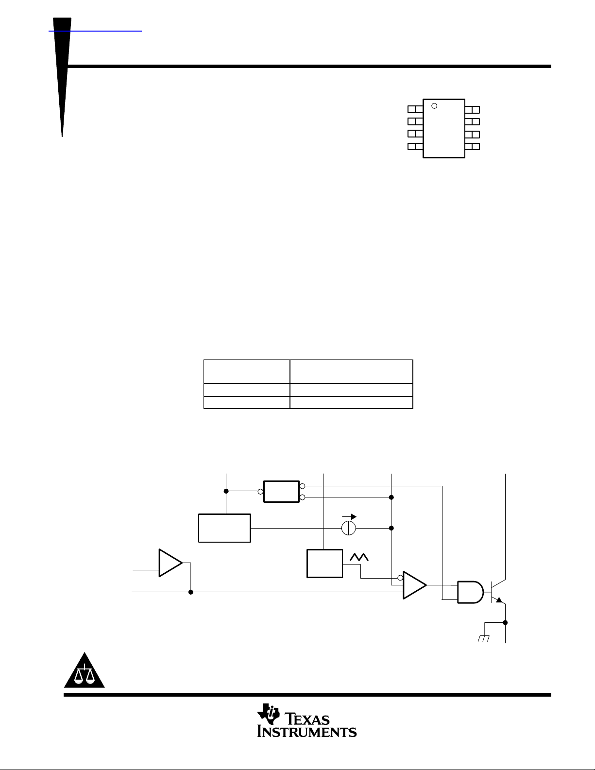
functional block diagram
V
Reference
Error
Amplifier
5
NI
INV
COMP
Please be aware that an important notice concerning availability, standard warranty, and use in critical applications of
Texas Instruments semiconductor products and disclaimers thereto appears at the end of this data sheet.
PRODUCTION DATA information is current as of publication date.
Products conform to specifications per the terms of Texas Instruments
standard warranty. Production processing does not necessarily include
testing of all parameters.
+
4
–
3
Voltage
CC
2
UVLO
2.5 V
RT
OSC
I
DT
DTC
67
PWM/DTC
Comparator
Copyright 2002, Texas Instruments Incorporated
OUT
GND
1
8
POST OFFICE BOX 655303 • DALLAS, TEXAS 75265
1
TL5002
PULSE-WIDTH-MODULATION CONTROL CIRCUIT
SLVS304A – SEPTEMBER 2000 – REVISED AUGUST 2002
detailed description
voltage reference
A 2.5-V regulator operating from V
is used to power the internal circuitry of the TL5002.
CC
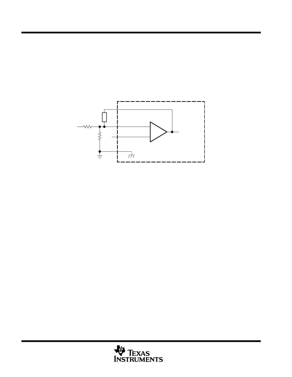
error amplifier
The error amplifier compares a sample of the dc-to-dc converter output voltage to an external reference voltage
and generates an error signal for the PWM comparator. The dc-to-dc converter output voltage is set by selecting
the error-amplifier gain (see Figure 1), using the following expression:
= (1 + R1/R2) (1 V)
V
O
TL5002
–
+
To PWM
Comparator
Compensation
V
I(FB)
Network
R1
R2
3
COMP
4
INV
5
ref
NI
GND8
V
Figure 1. Error-Amplifier Gain Setting
The error-amplifier output is brought out as COMP for use in compensating the dc-to-dc converter control loop
for stability . Because the amplifier can only source 45 µA, the total dc load resistance should be 100 kΩ or more.
oscillator/PWM
The oscillator frequency (f
) can be set between 20 kHz and 500 kHz by connecting a resistor between RT
osc
and GND. Acceptable resistor values range from 15 kΩ to 250 kΩ. The oscillator frequency can be determined
by using the graph shown in Figure 5.
The oscillator output is a triangular wave with a minimum value of approximately 0.7 V and a maximum value
of approximately 1.3 V. The PWM comparator compares the error-amplifier output voltage and the DTC input
voltage to the triangular wave and turns the output transistor off whenever the triangular wave is greater than
the lesser of the two inputs.
dead-time control (DTC)
DTC provides a means of limiting the output-switch duty cycle to a value less than 100%, which is critical for
boost and flyback converters. A current source generates a reference current (I
) at DTC that is nominally
DT
equal to the current at the oscillator timing terminal, RT . Connecting a resistor between DTC and GND generates
a dead-time reference voltage (V
as described in the previous section. Nominally , the maximum duty cycle is 0% when V
100% when V
is 1.3 V or greater. Because the triangle wave amplitude is a function of frequency and the
DT
source impedance of RT is relatively high (1250 Ω), choosing R
), which the PWM/DTC comparator compares to the oscillator triangle wave
DT
for a specific maximum duty cycle, D, is
DT
is 0.7 V or less and
DT
accomplished using the following equation and the voltage limits for the frequency in question as found in
Figure 11 (V
max and V
osc
min are the maximum and minimum oscillator levels):
osc
2
POST OFFICE BOX 655303 • DALLAS, TEXAS 75265
dead-time control (DTC) (continued)
TL5002
PULSE-WIDTH-MODULATION CONTROL CIRCUIT
SLVS304A – SEPTEMBER 2000 – REVISED AUGUST 2002
ǒ
Ǔ
–e
1
ƪ
DǒV
ǒ
–tńRDTC
C
max – V
osc
DT
DT
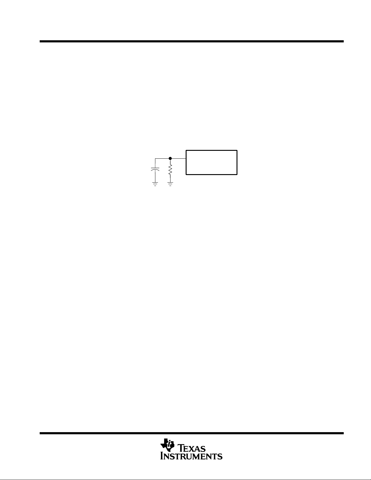
Figure 2. Soft-Start Circuit
osc
Ǔ
Ǔ
R
6
DT
minǓ) V
DTC
osc
TL5002
R
Where
R
DT
Soft start can be implemented by paralleling the DTC resistor with a capacitor (C
soft start, the voltage at DTC is derived by the following equation:
VDT[ IDTR
If the dc-to-dc converter must be in regulation within a specified period of time, the time constant, R
should be t
every time UVLO becomes active.
undervoltage-lockout (UVLO) protection
ǒ
+
DT
Rt) 1250
and Rt are in ohms, D in decimal
DT
/3 to t0/5. The TL5002 remains off until VDT ≈ 0.7 V, the minimum ramp value. CDT is discharged
0
min
ƫ
) as shown in Figure 2. During
DT
DTCDT
,
The undervoltage-lockout circuit turns the output transistor off whenever the supply voltage drops too low
(approximately 3 V at 25°C) for proper operation. A hysteresis voltage of 200 mV eliminates false triggering on
noise and chattering.
output transistor
The output of the TL5002 is an open-collector transistor with a maximum collector current rating of 21 mA and
a voltage rating of 51 V. The output is turned on under the following conditions: the oscillator triangle wave is
lower than both the DTC voltage and the error-amplifier output voltage, and the UVLO circuit is inactive.
POST OFFICE BOX 655303 • DALLAS, TEXAS 75265
3
TL5002
PULSE-WIDTH-MODULATION CONTROL CIRCUIT
SLVS304A – SEPTEMBER 2000 – REVISED AUGUST 2002
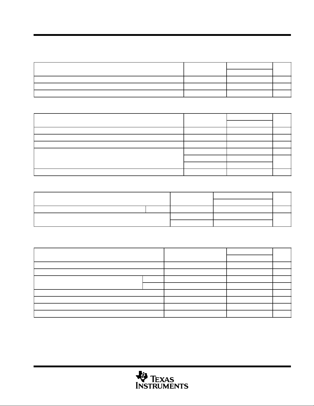
absolute maximum ratings over operating free-air temperature range (unless otherwise noted)
Supply voltage, V
Amplifier input voltage, V
Output voltage, V
Output current, I
Output peak current, I
Continuous total power dissipation See Dissipation Rating Table. . . . . . . . . . . . . . . . . . . . . . . . . . . . . . . . . . . . .
Operating ambient temperature range, T
Storage temperature range, T
Lead temperature 1,6 mm (1/16 inch) from case for 10 seconds 260°C. . . . . . . . . . . . . . . . . . . . . . . . . . . . . . .
†
Stresses beyond those listed under “absolute maximum ratings” may cause permanent damage to the device. These are stress ratings only, and
functional operation of the device at these or any other conditions beyond those indicated under “recommended operating conditions” is not
implied. Exposure to absolute-maximum-rated conditions for extended periods may affect device reliability.
NOTE 1: All voltage values are with respect to network ground terminal.
PACKAGE
D 725 mW 5.8 mW/°C 464 mW 377 mW 145 mW
(see Note 1) 41 V. . . . . . . . . . . . . . . . . . . . . . . . . . . . . . . . . . . . . . . . . . . . . . . . . . . . . . . . . . . .
CC
, OUT 51 V. . . . . . . . . . . . . . . . . . . . . . . . . . . . . . . . . . . . . . . . . . . . . . . . . . . . . . . . . . . . . . . . . . .
O
, OUT 21 mA. . . . . . . . . . . . . . . . . . . . . . . . . . . . . . . . . . . . . . . . . . . . . . . . . . . . . . . . . . . . . . . . . .
O
O(peak)
TA ≤ 25°C
POWER RATING
V
I(INV),
20 V. . . . . . . . . . . . . . . . . . . . . . . . . . . . . . . . . . . . . . . . . . . . . . . . . . . . . . . . .
I(NI)
, OUT 100 mA. . . . . . . . . . . . . . . . . . . . . . . . . . . . . . . . . . . . . . . . . . . . . . . . . . . . . . .
–40°C to 85°C. . . . . . . . . . . . . . . . . . . . . . . . . . . . . . . . . . . . . . . . . . . .
–65°C to 150°C. . . . . . . . . . . . . . . . . . . . . . . . . . . . . . . . . . . . . . . . . . . . . . . . . . .
stg
A
DISSIPATION RATING TABLE
DERATING FACTOR
ABOVE TA = 25°C
TA = 70°C
POWER RATING
TA = 85°C
POWER RATING
TA = 125°C
POWER RATING
recommended operating conditions
MIN MAX UNIT
Supply voltage, V
Amplifier input voltage, V
Output voltage, VO, OUT 50 V
Output current, IO, OUT 20 mA
COMP source current 45 µA
COMP dc load resistance 100 kΩ
Oscillator timing resistor, R
Oscillator frequency, f
Operating ambient temperature, T
CC
I(INV), VI(NI)
t
osc
A
3.6 40 V
0.9 1.5 V
15 250 kΩ
20 500 kHz
–40 85 °C
†
4
POST OFFICE BOX 655303 • DALLAS, TEXAS 75265
TL5002
Frequency change with tem erature
PULSE-WIDTH-MODULATION CONTROL CIRCUIT
SLVS304A – SEPTEMBER 2000 – REVISED AUGUST 2002
electrical characteristics over recommended operating free-air temperature range, VCC = 6 V,
f
= 100 kHz (unless otherwise noted)
osc
undervoltage lockout
PARAMETER TEST CONDITIONS
Upper threshold voltage TA = 25°C 3 V
Lower threshold voltage TA = 25°C 2.8 V
Hysteresis TA = 25°C 100 200 mV
†
All typical values are at TA = 25°C.
oscillator
PARAMETER TEST CONDITIONS
Frequency Rt = 100 kΩ 100 kHz
Standard deviation of frequency 15 kHz
Frequency change with voltage VCC = 3.6 V to 40 V 1 kHz
TA = –40°C to 25°C –4 –0.4 4 kHz
Frequency change with temperature
Voltage at RT 1 V
†
All typical values are at TA = 25°C.
TA = –20°C to 25°C –4 –0.4 4 kHz
TA = 25°C to 85°C –4 –0.2 4 kHz
TL5002C
MIN TYP†MAX
TL5002C
MIN TYP†MAX
UNIT
UNIT
dead-time control
PARAMETER TEST CONDITIONS
Output (source) current TL5002 V
p
Input threshold voltage
†
All typical values are at TA = 25°C.
‡
Output source current at RT
= 1.5 V 0.9 × I
(DT)
Duty cycle = 0% 0.5 0.7
Duty cycle = 100% 1.3 1.5
TL5002C
MIN TYP†MAX
RT
‡
1.2 × I
UNIT
RT
error amplifier
PARAMETER TEST CONDITIONS
Input voltage VCC = 3.6 V to 40 V 0.3 1.5 V
Input bias current –160 –500 nA
Output voltage swing
Open-loop voltage amplification 80 dB
Unity-gain bandwidth 1.5 MHz
Output (sink) current V
Output (source) current V
†
All typical values are at TA = 25°C.
Positive 1.5 2.3 V
Negative 0.3 0.4 V
= 1.2 V , COMP = 1 V 100 600 µA
I(INV)
= 0.8 V , COMP = 1 V –45 –70 µA
I(INV)
TL5002C
MIN TYP†MAX
UNIT
µA
V
POST OFFICE BOX 655303 • DALLAS, TEXAS 75265
5

TL5002
PULSE-WIDTH-MODULATION CONTROL CIRCUIT
SLVS304A – SEPTEMBER 2000 – REVISED AUGUST 2002
electrical characteristics over recommended operating free-air temperature range, VCC = 6 V,
f
= 100 kHz (unless otherwise noted) (continued)
osc
output
PARAMETER TEST CONDITIONS
Output saturation voltage IO = 10 mA 1.5 2 V
Off-state current
Short-circuit output current VO = 6 V 40 mA
†
All typical values are at TA = 25°C.
VO = 50 V, VCC = 0 10
VO = 50 V 10
total device
PARAMETER TEST CONDITIONS
Standby supply current Off state 1 1.5 mA
Average supply current Rt = 100 kΩ 1.4 2.1 mA
†
All typical values are at TA = 25°C.
TL5002C
MIN TYP†MAX
TL5002C
MIN TYP†MAX
UNIT
UNIT
µA
DTC
OSC
PWM/DTC
Comparator
OUT
V
CC
PARAMETER MEASUREMENT INFORMATION
COMP
3 V
Figure 3. PWM Timing Diagram
6
POST OFFICE BOX 655303 • DALLAS, TEXAS 75265

PULSE-WIDTH-MODULATION CONTROL CIRCUIT
SLVS304A – SEPTEMBER 2000 – REVISED AUGUST 2002
TYPICAL CHARACTERISTICS
TL5002
OSCILLATOR FREQUENCY
vs
TIMING RESISTANCE
1 M
VCC = 6 V
DT Resistance = R
TA = 25°C
100 k
– Oscillator Frequency – Hz
osc
f
10 k
10 k 100 k 1 M
Rt – Timing Resistance – Ω
t
Figure 4
100
98
96
94
92
90
osc
f – Oscillation Frequency – kHz
88
– 50 – 25 0
OSCILLATION FREQUENCY
vs
AMBIENT TEMPERATURE
VCC = 6 V
Rt = 100 kΩ
DT Resistance = 100 kΩ
25 50 75 100
TA – Ambient Temperature – °C
Figure 5
AVERAGE SUPPLY CURRENT
vs
POWER-SUPPLY VOLTAGE
2
Rt = 100 kΩ
TA = 25 °C
1.5
1
0.5
– Average Supply Current – mA
CC
I
0
010203040
VCC – Power-Supply Voltage – V
Figure 6
1.3
1.2
1.1
1
0.9
– Average Supply Current – mA
0.8
CC
I
0
– 50 – 25 0
AVERAGE SUPPLY CURRENT
vs
AMBIENT TEMPERATURE
VCC = 6 V
Rt = 100 kΩ
DT Resistance = 100 kΩ
25 50 75
TA – Ambient Temperature – °C
Figure 7
100
POST OFFICE BOX 655303 • DALLAS, TEXAS 75265
7

TL5002
PULSE-WIDTH-MODULATION CONTROL CIRCUIT
SLVS304A – SEPTEMBER 2000 – REVISED AUGUST 2002
TYPICAL CHARACTERISTICS
PWM TRIANGLE WAVE AMPLITUDE VOLTAGE
vs
OSCILLATOR FREQUENCY
1.8
VCC = 6 V
TA = 25 °C
1.5
V
max (100% duty cycle)
1.2
0.9
0.6
0.3
PWM Triangle Wave Amplitude Voltage – V
0
10 k 100 k 1 M 10 M
f
osc
osc
V
min (zero duty cycle)
osc
– Oscillator Frequency – Hz
Figure 8
ERROR AMPLIFIER OUTPUT VOLTAGE
OUTPUT (SINK) CURRENT
3
VCC = 6 V
V
= 1.2 V
I(INV)
V
= 1 V
I(NI)
2.5
TA = 25
2
1.5
1
– Error Amplifier Output Voltage – V
0.5
O
V
0
0 0.2 0.4
°C
IO – Output (Sink) Current – mA
vs
0.6
Figure 9
ERROR AMPLIFIER OUTPUT VOLTAGE
3
2.5
2
1.5
1
VCC = 6 V
V
I(INV)
0.5
– Error Amplifier Output Voltage – V
O
V
V
I(NI)
TA = 25 °C
0
02040
vs
OUTPUT (SOURCE) CURRENT
= 0.8 V
= 1 V
60 80 100
IO – Output (Source) Current – µA
Figure 10
120
2.46
VCC = 6 V
V
V
2.45
No Load
2.44
2.43
2.42
2.41
– Error Amplifier Output Voltage – V
O
V
2.40
– 50 – 25 0
ERROR AMPLIFIER OUTPUT VOLTAGE
vs
AMBIENT TEMPERATURE
= 0.8 V
I(INV)
= 1 V
I(NI)
25 50 75
TA – Ambient Temperature – °C
Figure 11
100
8
POST OFFICE BOX 655303 • DALLAS, TEXAS 75265

PULSE-WIDTH-MODULATION CONTROL CIRCUIT
SLVS304A – SEPTEMBER 2000 – REVISED AUGUST 2002
TYPICAL CHARACTERISTICS
TL5002
ERROR AMPLIFIER OUTPUT VOLTAGE
240
VCC = 6 V
V
V
220
No Load
200
180
160
– Error Amplifier Output Voltage – mV
140
O
V
120
– 50 – 25 0
vs
AMBIENT TEMPERATURE
= 1.2 V
I(INV)
= 1 V
I(NI)
25 50 75
TA – Ambient Temperature – °C
Figure 12
120
VCC = 6 V
Rt = 100 kΩ
TA = 25 °C
100
80
60
40
Output Duty Cycle – %
20
0
100
0 0.5 1
ERROR AMPLIFIER CLOSED-LOOP GAIN AND
PHASE SHIFT
vs
FREQUENCY
40
VCC = 6 V
TA = 25 °C
30
OUTPUT DUTY CYCLE
vs
DTC VOLTAGE
1.5 2
DTC Voltage – V
Figure 13
–180°
–210°
20
A
V
10
0
– 10
– 20
– Error Amplifier Closed-Loop Gain and Phase Shift – dB
10 k 100 k 1 M 10 M
V
A
f – Frequency – Hz
φ
Figure 14
POST OFFICE BOX 655303 • DALLAS, TEXAS 75265
–240°
–270°
– Phase Shift φ
–300°
–330°
–360°
9

TL5002
PULSE-WIDTH-MODULATION CONTROL CIRCUIT
SLVS304A – SEPTEMBER 2000 – REVISED AUGUST 2002
TYPICAL CHARACTERISTICS
– 60
– 50
AµI
– 40
– 30
– 20
– DTC Output Current –
O(DT)
– 10
0
0 – 10 – 20
DTC OUTPUT CURRENT
RT OUTPUT CURRENT
DT Voltage = 1.3 V
TA = 25 °C
IO – RT Output Current – µA
Figure 15
vs
– 30 – 40 – 50
– 60
OUTPUT SATURATION VOLTAGE
vs
OUTPUT (SINK) CURRENT
2
VCC = 6 V
TA = 25 °C
1.5
1
0.5
– Output Saturation Voltage – V
CE
V
0
0 5 10 15 20
IO – Output (Sink) Current – mA
Figure 16
10
POST OFFICE BOX 655303 • DALLAS, TEXAS 75265

PULSE-WIDTH-MODULATION CONTROL CIRCUIT
SLVS304A – SEPTEMBER 2000 – REVISED AUGUST 2002
APPLICATION INFORMATION
VTT
GND
+ +
TL5002
2
6
VCC
6
7
8
4
+
JP1
BOOT
VCC
3
HIGHDR
BOOTLO
DT
5
LOWDR
IN2PGND
1
3
DTC
COMP
OUT5NI
1
7
4
8
RT
INV
GND
Figure 17. DDRI Application
POST OFFICE BOX 655303 • DALLAS, TEXAS 75265
11

TL5002
PULSE-WIDTH-MODULATION CONTROL CIRCUIT
SLVS304A – SEPTEMBER 2000 – REVISED AUGUST 2002
APPLICATION INFORMATION
PARTIAL BILL OF MATERIALS
QUANTITY
1 C1 UUD1C471MNR1GS Capacitor, aluminum Nichicon 0.327 x 0.327
6 C2 – C6, C13 EMK325BJ106MN–B Capacitor, ceramic Taiyo Yuden 1210
3 C7, C8, C20 GRM40X7R105K16PT Capacitor, ceramic, jumper Murata 805
2 C9, C10 EEF–CD0D101R Capacitor, aluminum Panasonic 7343
1 C14 08055A102JAT2A Capacitor, ceramic AVX 805
1 C15 GRM39X7R104K016D Capacitor, ceramic Murata 603
1 C16 NMC0805X7R224K16TR Capacitor , ceramic NIP 603
1 C17 VJ0603Y222KXANT Capacitor, ceramic Murata 603
1 C18 C0603C223J3RACTU Capacitor, ceramic Kemet 603
1 C19 GRM39X7R223K16 Capacitor, ceramic Murata 603
1 D1 1SMB5919BT3 Diode, zener, 5.6 V On Semi SMB
2 J1, J2 ED1609 Terminal block, 2-pin OST
1 J3 PTC36SAAN Header, 4-pin Sullins
1 JP1 PTC36SAAN Header , 2-pin Sullins
1 L1 UP2B–1R0 Inductor, SMT Coiltronics 0.55 x 0.41
1 L2 UP4B–2R2 Inductor, SMT Coiltronics
4 Q1 – Q4 IRF7811 MOSFET, N–ch, 30 V IR SO8
3 R1, R2, R4 Std Resistor, chip, 4.7 Ω Std 603
1 R3 Std Resistor, chip, 2.49 KΩ Std 603
2 R5, R6 Std Resistor, chip, 0 Ω Std 603
1 R7 Std Resistor, chip, 20 KΩ Std 603
1 R8 Std Resistor, chip, 162 KΩ Std 603
1 R9 Std Resistor, chip, 1.74 KΩ Std 603
1 R10 Std Resistor, chip, 7.32 KΩ Std 603
1 R11 Std Open Std 603
1 R12 Std Resistor, chip, 15 KΩ Std 603
1 R13 Std Resistor, chip, 10 Ω Std 603
1 R14 Std Resistor, chip, 10 KΩ Std 603
4 TP1 – TP3, TP5 240-345 Test point, red, 1 mm Farnell 0.038
1 TP4 131-4244-00 or 131-5031-00 Adaptor, 3.5 mm probe Tektronix 0.200
1 TP6 1045-3-17-15-30-14-02-0 Post, wirewrap Mill-Max 0.043
1 U1 TPS2837D IC, MOSFET driver Texas Instruments SO8
1 U2 TL5002D IC, low-cost PMW Texas Instruments SO8
REF DES PART NUMBER DESCRIPTION MANUFACTURER SIZE
12
POST OFFICE BOX 655303 • DALLAS, TEXAS 75265

TL5002
PULSE-WIDTH-MODULATION CONTROL CIRCUIT
SLVS304A – SEPTEMBER 2000 – REVISED AUGUST 2002
MECHANICAL DATA
D (R-PDSO-G**) PLASTIC SMALL-OUTLINE PACKAGE
14 PIN SHOWN
0.050 (1,27)
14
1
0.069 (1,75) MAX
0.020 (0,51)
0.014 (0,35)
8
7
A
0.010 (0,25)
0.004 (0,10)
DIM
0.157 (4,00)
0.150 (3,81)
PINS **
0.010 (0,25)
0.244 (6,20)
0.228 (5,80)
8
M
Seating Plane
0.004 (0,10)
14
0.008 (0,20) NOM
0°–ā8°
16
Gage Plane
0.010 (0,25)
0.044 (1,12)
0.016 (0,40)
A MAX
A MIN
NOTES: A. All linear dimensions are in inches (millimeters).
B. This drawing is subject to change without notice.
C. Body dimensions do not include mold flash or protrusion, not to exceed 0.006 (0,15).
D. Falls within JEDEC MS-012
POST OFFICE BOX 655303 • DALLAS, TEXAS 75265
0.197
(5,00)
0.189
(4,80)
0.344
(8,75)
0.337
(8,55)
0.394
(10,00)
0.386
(9,80)
4040047/D 10/96
13

IMPORTANT NOTICE
Texas Instruments Incorporated and its subsidiaries (TI) reserve the right to make corrections, modifications,
enhancements, improvements, and other changes to its products and services at any time and to discontinue
any product or service without notice. Customers should obtain the latest relevant information before placing
orders and should verify that such information is current and complete. All products are sold subject to TI’s terms
and conditions of sale supplied at the time of order acknowledgment.
TI warrants performance of its hardware products to the specifications applicable at the time of sale in
accordance with TI’s standard warranty . Testing and other quality control techniques are used to the extent TI
deems necessary to support this warranty . Except where mandated by government requirements, testing of all
parameters of each product is not necessarily performed.
TI assumes no liability for applications assistance or customer product design. Customers are responsible for
their products and applications using TI components. T o minimize the risks associated with customer products
and applications, customers should provide adequate design and operating safeguards.
TI does not warrant or represent that any license, either express or implied, is granted under any TI patent right,
copyright, mask work right, or other TI intellectual property right relating to any combination, machine, or process
in which TI products or services are used. Information published by TI regarding third–party products or services
does not constitute a license from TI to use such products or services or a warranty or endorsement thereof.
Use of such information may require a license from a third party under the patents or other intellectual property
of the third party , or a license from TI under the patents or other intellectual property of TI.
Reproduction of information in TI data books or data sheets is permissible only if reproduction is without
alteration and is accompanied by all associated warranties, conditions, limitations, and notices. Reproduction
of this information with alteration is an unfair and deceptive business practice. TI is not responsible or liable for
such altered documentation.
Resale of TI products or services with statements different from or beyond the parameters stated by TI for that
product or service voids all express and any implied warranties for the associated TI product or service and
is an unfair and deceptive business practice. TI is not responsible or liable for any such statements.
Mailing Address:
Texas Instruments
Post Office Box 655303
Dallas, Texas 75265
Copyright 2002, Texas Instruments Incorporated
 Loading...