

Page 1
www.DataSheet4U.com
www.ti.com
2.5-V to 5-V DUAL UART WITH 16-BYTE FIFOS
TL16C2550
SLWS161 – JUNE 2005
FEATURES
• Internal Diagnostic Capabilities:
• Programmable Auto-RTS and Auto-CTS – Loopback Controls for Communications
• In Auto-CTS Mode, CTS Controls Transmitter
• In Auto-RTS Mode, RCV FIFO Contents and
Threshold Control RTS
• Serial and Modem Control Outputs Drive a
Link Fault Isolation
– Break, Parity, Overrun, and Framing Error
Simulation
• Fully Prioritized Interrupt System Controls
RJ11 Cable Directly When Equipment Is on • Modem Control Functions ( CTS, RTS, DSR,
the Same Power Drop DTR, RI, and DCD)
• Capable of Running With All Existing • Available in 48-Pin TQFP (PFB), 44-Pin PLCC
TL16C450 Software (FN), or 32-Pin QFN (RHB) Packages
• After Reset, All Registers Are Identical to the • Pin Compatible with TL16C752B (48-Pin
TL16C450 Register Set Package)
• Up to 24-MHz Clock Rate for up to 1.5-Mbaud
Operation With V
= 5 V
CC
• Up to 20-MHz Clock Rate for up to 1.25-Mbaud
Operation With V
= 3.3 V
CC
• Up to 16-MHz Clock Rate for up to 1-Mbaud
Operation With V
= 2.5 V
CC
• In the TL16C450 Mode, Hold and Shift
Registers Eliminate the Need for Precise
APPLICATIONS
• Point-of-Sale Terminals
• Gaming Terminals
• Portable Applications
• Router Control
• Cellular Data
• Factory Automation
Synchronization Between the CPU and Serial
Data
• Programmable Baud Rate Generator Allows
Division of Any Input Reference Clock by 1 to
16
(2
- 1) and Generates an Internal 16 × Clock
• Standard Asynchronous Communication Bits
(Start, Stop, and Parity) Added to or Deleted
From the Serial Data Stream
• 5-V, 3.3-V, and 2.5-V Operation
• Independent Receiver Clock Input
• Transmit, Receive, Line Status, and Data Set
Interrupts Independently Controlled
DESCRIPTION
The TL16C2550 is a dual universal asynchronous
receiver and transmitter (UART). It incorporates the
functionality of two TL16C550D UARTs, each UART
having its own register set and FIFOs. The two
UARTs share only the data bus interface and clock
source, otherwise they operate independently.
Another name for the uart function is Asynchronous
Communications Element (ACE), and these terms will
be used interchangeably. The bulk of this document
will describe the behavior of each ACE, with the
understanding that two such devices are incorporated
into the TL16C2550.
• Fully Programmable Serial Interface
Characteristics:
– 5-, 6-, 7-, or 8-Bit Characters
– Even-, Odd-, or No-Parity Bit Generation and
Detection
– 1-, 1 1/2-, or 2-Stop Bit Generation
– Baud Generation (dc to 1 Mbit/s)
• False-Start Bit Detection
• Complete Status Reporting Capabilities
• 3-State Output TTL Drive Capabilities for
Bidirectional Data Bus and Control Bus
• Line Break Generation and Detection
Please be aware that an important notice concerning availability, standard warranty, and use in critical applications of Texas
Instruments semiconductor products and disclaimers thereto appears at the end of this data sheet.
PRODUCT PREVIEW information concerns products in the formative or design phase of development. Characteristic data and other
specifications are design goals. Texas Instruments reserves the
right to change or discontinue these products without notice.
Copyright © 2005, Texas Instruments Incorporated
Page 2
www.ti.com
PRODUCT PREVIEW
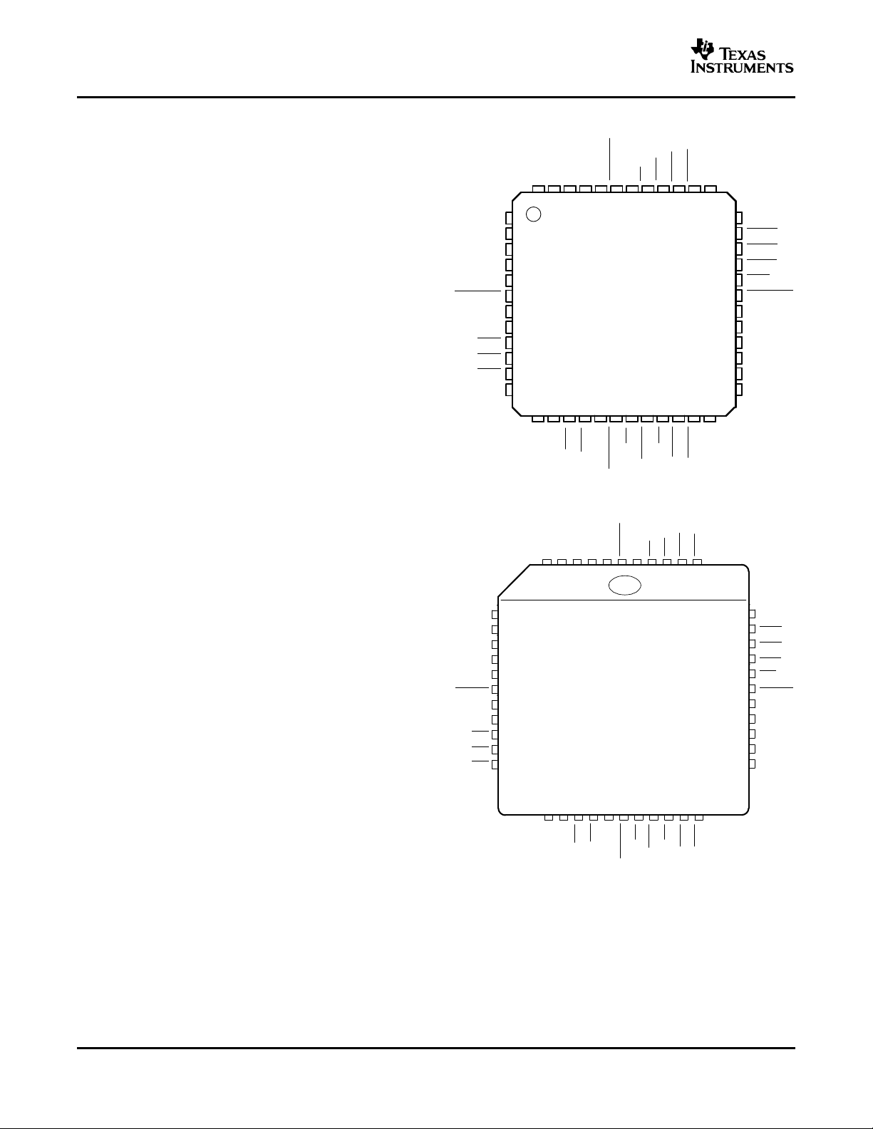
NC−No internal connection
14 15
RESET
DTRB
DTRA
RTSA
OPA
RXRDYA
INTA
INTB
A0
A1
A2
NC
36
35
34
33
32
31
30
29
28
27
26
25
16
1
2
3
4
5
6
7
8
9
10
11
12
D5
D6
D7
RXB
RXA
TXRDYB
TXA
TXB
OPB
CSA
CSB
NC
17 18 19 20
PFB PACKAGE
(TOP VIEW)
RA
CDA
DSRA
CTSA
47 46 45 44 4348 42
D4D3D2D1D0
TXRDYA
RTSB
CTSB
NC
IOW
CDB
GND
IOR
DSRB
RIB
40 39 3841
21
22 23 24
37
13
XTAL1
NC
V
CC
XTAL2
RXRDYB
TL16C2550PFB
RESET
OPA
D5
D6
A0
A2
A1
INTB
INTA
RXRDYA
RTSA
DTRA
DTRB
39
35
31
29
30
32
33
34
36
37
38
246 1 42 4041434435
7
8
9
10
11
12
13
14
15
16
17
1918 26 2820 21 22 23 24 25 27
RXB
RXA
TXRDYB
TXA
TXB
OPB
CSA
CSB
D7
IOW
XTAL1
XTAL2
CDB
GND
RXRDYB
IOR
DSRB
RIB
RTSB
CTSB
D4
D0
CDA
CTSA
DSRA
RIA
V
CC
TXRDYA
D1
D2
D3
TL16C2550FN
FN PACKAGE
(TOP VIEW)
TL16C2550
SLWS161 – JUNE 2005
Each ACE is a speed and voltage range upgrade of
the TL16C550C, which in turn is a functional upgrade
of the TL16C450. Functionally equivalent to the
TL16C450 on power up or reset (single character or
TL16C450 mode), each ACE can be placed in an
alternate FIFO mode. This relieves the CPU of
excessive software overhead by buffering received
and to be transmitted characters. Each receiver and
transmitter store up to 16 bytes in their respective
FIFOs, with the receive FIFO including three additional bits per byte for error status. In the FIFO
mode, a selectable autoflow control feature can
significantly reduce software overload and increase
system efficiency by automatically controlling serial
data flow using handshakes between the RTS#
output and CTS# input, thus eliminating overruns in
the receive FIFO.
Each ACE performs serial-to-parallel conversions on
data received from a peripheral device or modem and
stores the parallel data in its receive buffer or FIFO,
and each ACE performs parallel-to-serial conversions
on data sent from its CPU after storing the parallel
data in its transmit buffer or FIFO. The CPU can read
the status of either ACE at any time. Each ACE
includes complete modem control capability and a
processor interrupt system that can be tailored to the
application.
Each ACE includes a programmable baud rate generator capable of dividing a reference clock with divisors of from 1 to 65535, thus producing a 16×
internal reference clock for the transmitter and receiver logic. Each ACE accommodates up to a
1.5-Mbaud serial data rate (24-MHz input clock). As a
reference point, that speed would generate a 667-ns
bit time and a 6.7-µs character time (for 8,N,1 serial
data), with the internal clock running at 24 MHz.
Each ACE has a TXRDY# and RXRDY# output that
can be used to interface to a DMA controller.
2
Page 3
www.ti.com
1
2
3
4
5
6
7
8
9
10
11
12
13
14
15
16
24
23
22
21
20
19
18
17
D6
D7
RXB
RXA
TXA
TXB
CSA
CSB
RESET
RTSA
INTA
INTB
A0
A1
A2
NC
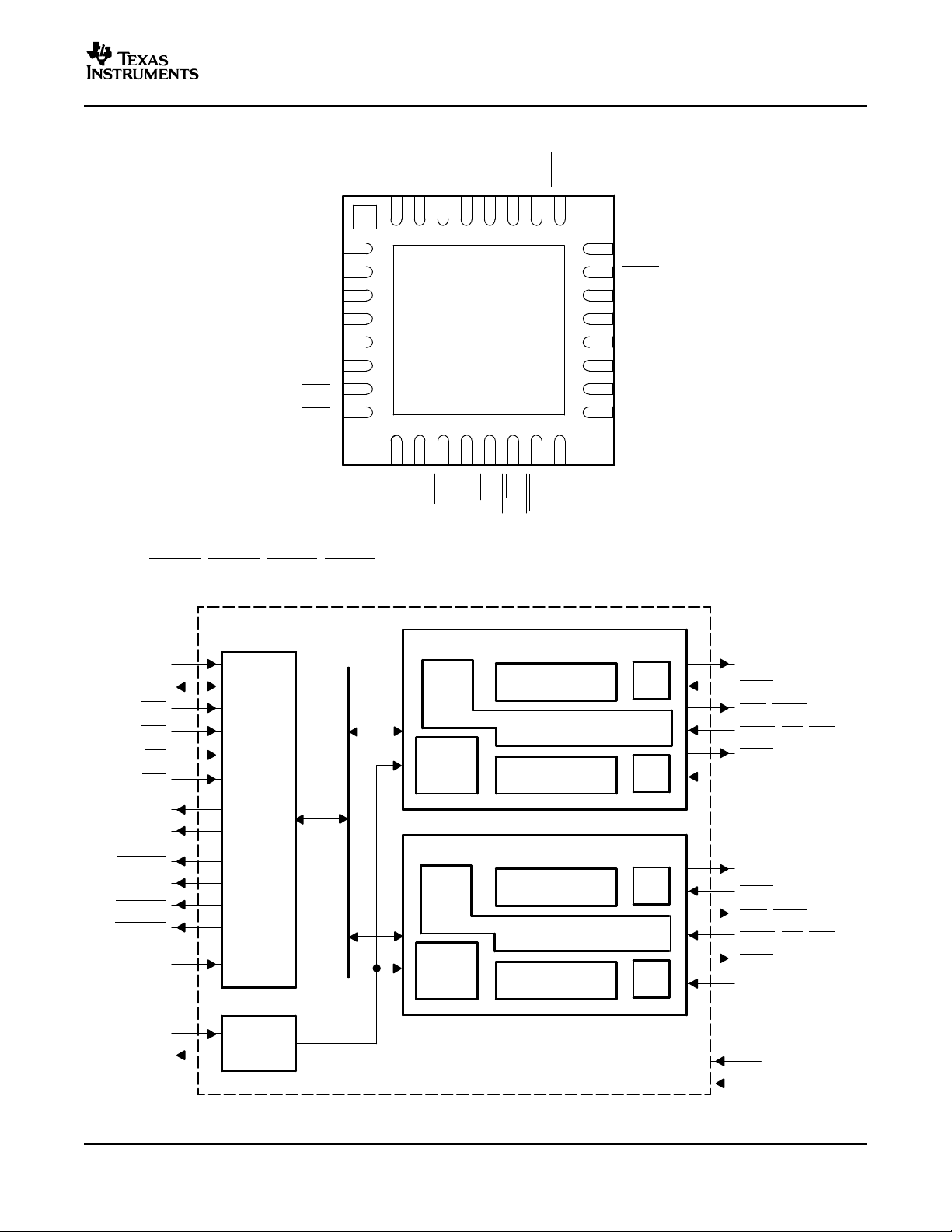
32
31
30
29
28
27
26
25
D5D4D3D2D1D0VCCCTSA
NC
XTAL1
XTAL2
IOW
GND
IOR
RTSB
CTSB
RHB PACKAGE
(TOP VIEW)
NC − No internal connection
TL16C2550RHB
Crystal
OSC
Buffer
Data Bus
Interface
A2 − A0
D7 − D0
CSA
CSB
IOR
IOW
INTA
INTB
TXRDYA
TXRDYB
RXRDYA
RXRDYB
RESET
XTAL1
XTAL2
BAUD
Rate
Gen
16 Byte Tx FIFO
16 Byte Rx FIFO
Tx
Rx
UART Channel A
BAUD
Rate
Gen
16 Byte Tx FIFO
16 Byte Rx FIFO
Tx
Rx
UART Channel B
CTSA
OPA, DTRA
DSRA, RIA, CDA
RTSA
CTSB
OPB, DTRB
DSRB, RIB, CDB
RTSB
V
CC
GND
TXA
RXA
TXB
RXB
UART Regs
UART Regs
TL16C2550
SLWS161 – JUNE 2005
NOTE: The 32-pin RHB package does not provide access to DSRA, DRRB, RIA, RIB, CDA, CDB inputs, and OPA, OPB,
RXRDYA, RXRDYB, TXRDYA, TXRDYB outputs.
Figure 1. TL16C2550 Block Diagram
3
Page 4
www.ti.com
PRODUCT PREVIEW
TL16C2550
SLWS161 – JUNE 2005
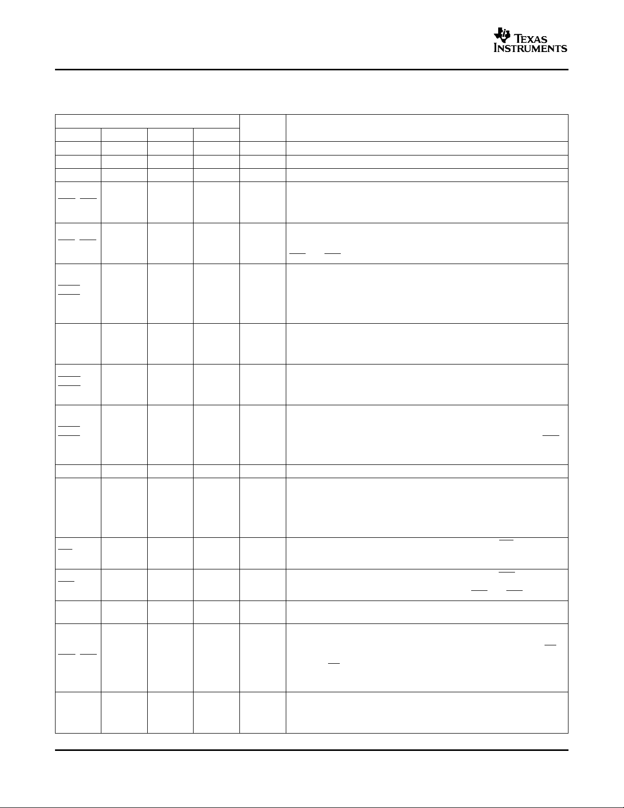
TERMINAL
NAME PFB NO. FN NO. RHB NO.
A0 28 31 20 I Address 0 select bit. Internal registers address selection
A1 27 30 19 I Address 1 select bit. Internal registers address selection
A2 26 29 18 I Address 2 select bit. Internal registers address selection
CDA, CDB 40, 16 42, 21 – I
CSA, CSB 10, 11 16, 17 7, 8 I
CTSA, or data set is ready to accept transmit data from the 2550. Status can be
CTSB tested by reading MSR bit 4. These pins only affect the transmit and receive
D0-D4 44 - 48 2 - 6 27 - 31 Data bus (bidirectional). These pins are the eight bit, 3-state data bus for
D5-D7 1 - 3 7 - 9 32, 1, 2
DSRA, UART channels A and B. A logic low on these pins indicates the modem or
DSRB data set is powered on and is ready for data exchange with the UART. The
DTRA, theTLl16C2550 is powered on and ready. These pins can be controlled
DTRB through the modem control register. Writing a 1 to MCR bit 0 sets the DTR
GND 17 22 13 Signal and power ground.
INTA, a logic 1, interrupt sources are enabled in the interrupt enable register
INTB (IER). Interrupt conditions include: receiver errors, available receiver buffer
IOR 19 24 14 I contents of an internal register defined by address bits A0-A2 onto the
IOW 15 20 12 I the contents of the data bus (D0-D7) from the external CPU to an internal
NC – 9, 17 No internal connection
OPA, OPB 32, 9 35, 15 – O a logic 0 when the MCR-3 is set to a logic 1. INTA-B are set to the 3-state
RESET 36 39 24 I
38, 23 40, 28 25, 16 I
39, 20 41, 25 – I
34, 35 37, 38 – O
30, 29 33, 32 22, 21 O
12, 24, 25,
37
DEVICE INFORMATION
TERMINAL FUNCTIONS
I/O DESCRIPTION
Carrier detect (active low). These inputs are associated with individual
UART channels A and B. A low on these pins indicates that a carrier has
been detected by the modem for that channel. The state of these inputs is
reflected in the modem status register (MSR).
Chip select A and B (active low). These pins enable data transfers between
the user CPU and the TL16C2550 for the channel(s) addressed. Individual
UART sections (A, B) are addressed by providing a low on the respective
CSA and CSB pins.
Clear to send (active low). These inputs are associated with individual
UART channels A and B. A logic low on the CTS pins indicates the modem
operations when auto CTS function is enabled through the enhanced
feature register (EFR) bit 7, for hardware flow control operation.
I/O
transferring information to or from the controlling CPU. D0 is the least
significant bit and the first data bit in a transmit or receive serial data
stream.
Data set ready (active low). These inputs are associated with individual
state of these inputs is reflected in the modem status register (MSR).
Data terminal ready (active low). These outputs are associated with
individual UART channels A and B. A logic low on these pins indicates that
output to low, enabling the modem. The output of these pins is high after
writing a 0 to MCR bit 0, or after a reset.
Interrupt A and B (active high). These pins provide individual channel
interrupts, INT A and B. INT A and B are enabled when MCR bit 3 is set to
data, available transmit buffer space or when a modem status flag is
detected. INTA-B are in the high-impedance state after reset.
Read input (active low strobe). A high to low transition on IOR will load the
TL16C2550 data bus (D0-D7) for access by an external CPU.
Write input (active low strobe). A low to high transition on IOW will transfer
register that is defined by address bits A0-A2 and CSA and CSB
User defined outputs. This function is associated with individual channels A
and B. The state of these pins is defined by the user through the software
settings of the MCR register, bit 3. INTA-B are set to active mode and OP to
mode and OP to a logic 1 when MCR-3 is set to a logic 0. See bit 3,
modem control register (MCR bit 3). The output of these two pins is high
after reset.
Reset. RESET will reset the internal registers and all the outputs. The
UART transmitter output and the receiver input will be disabled during reset
time. See TL16C2550 external reset conditions for initialization details.
RESET is an active-high input.
4
Page 5
www.ti.com
SLWS161 – JUNE 2005
DEVICE INFORMATION (continued)
TERMINAL FUNCTIONS (continued)
TERMINAL
NAME PFB NO. FN NO. RHB NO.
RIA, RIB 41, 21 43, 26 – I
RTSA,
RTSB
RXA, RXB 5, 4 11, 10 4, 3 I
RXRDYA,
RXRDYB
TXA, TXB 7, 8 13, 14 5, 6 O channel data from the 2550. During the local loopback mode, the TX input
TXRDYA,
TXRDYB
V
CC
XTAL1 13 18 10 I
XTAL2 14 19 11 O
33, 22 36, 27 23, 15 O (MCR bit 1) sets these pins to low, indicating data is available. After a reset,
31, 18 34, 23 – O level has been reached or a timeout interrupt occurs. They go high when
43, 6 11, 12 – O a trigger level numbers of spaces available. They go high when the TX
42 44 26 I Power supply inputs.
I/O DESCRIPTION
Ring indicator (active low). These inputs are associated with individual
UART channels A and B. A logic low on these pins indicates the modem
has received a ringing signal from the telephone line. A low to high
transition on these input pins generates a modem status interrupt, if
enabled. The state of these inputs is reflected in the modem status register
(MSR)
Request to send (active low). These outputs are associated with individual
UART channels A and B. A low on the RTS pin indicates the transmitter has
data ready and waiting to send. Writing a 1 in the modem control register
these pins are set to high. These pins only affects the transmit and receive
operation when auto RTS function is enabled through the enhanced feature
register (EFR) bit 6, for hardware flow control operation.
Receive data input. These inputs are associated with individual serial
channel data to the 2550. During the local loopback mode, these RX input
pins are disabled and TX data is internally connected to the UART RX input
internally.
Receive ready (active low). RXRDY A and B goes low when the trigger
the RX FIFO is empty or there is an error in RX FIFO.
Transmit data. These outputs are associated with individual serial transmit
pin is disabled and TX data is internally connected to the UART RX input.
Transmit ready (active low). TXRDY A and B go low when there are at least
buffer is full.
Crystal or external clock input. XTAL1 functions as a crystal input or as an
external clock input. A crystal can be connected between XTAL1 and
XTAL2 to form an internal oscillator circuit (see Figure 10). Alternatively, an
external clock can be connected to XTAL1 to provide custom data rates.
Output of the crystal oscillator or buffered clock. See also XTAL1. XTAL2 is
used as a crystal oscillator output or buffered a clock output.
TL16C2550
Detailed Description
Autoflow Control (see Figure 2)
Autoflow control is comprised of auto- CTS and auto- RTS. With auto- CTS, the CTS input must be active before
the transmitter FIFO can emit data. With auto- RTS, RTS becomes active when the receiver needs more data and
notifies the sending serial device. When RTS is connected to CTS, data transmission does not occur unless the
receiver FIFO has space for the data; thus, overrun errors are eliminated using ACE1 and ACE2 from a
TLC16C2550 with the autoflow control enabled. If not, overrun errors occur when the transmit data rate exceeds
the receiver FIFO read latency.
5
Page 6
www.ti.com
PRODUCT PREVIEW
RCV
FIFO
Serial to
Parallel
Flow
Control
XMT
FIFO
Parallel
to Serial
Flow
Control
Parallel
to Serial
Flow
Control
Serial to
Parallel
Flow
Control
XMT
FIFO
RCV
FIFO
ACE1 ACE2
D7−D0
SIN SOUT
RTS CTS
SOUT SIN
CTS RTS
D7−D0
Start Bits 0−7 Start Bits 0−7 Start Bits 0−7
Stop Stop Stop
SOUT
CTS
TL16C2550
SLWS161 – JUNE 2005
Figure 2. Autoflow Control (Auto- RTS and Auto- CTS) Example
Auto- RTS (see Figure 2)
Auto- RTS data flow control originates in the receiver timing and control block (see functional block diagram) and
is linked to the programmed receiver FIFO trigger level. When the receiver FIFO level reaches a trigger level of
1, 4, or 8 (see Figure 3), RTS is deasserted. With trigger levels of 1, 4, and 8, the sending ACE may send an
additional byte after the trigger level is reached (assuming the sending ACE has another byte to send) because it
may not recognize the deassertion of RTS until after it has begun sending the additional byte. RTS is
automatically reasserted once the RCV FIFO is emptied by reading the receiver buffer register.
When the trigger level is 14 (see Figure 4), RTS is deasserted after the first data bit of the 16th character is
present on the RX line. RTS is reasserted when the RCV FIFO has at least one available byte space.
Auto- CTS (see Figure 2)
The transmitter circuitry checks CTS before sending the next data byte. When CTS is active, it sends the next
byte. To stop the transmitter from sending the following byte, CTS must be released before the middle of the last
stop bit that is currently being sent (see Figure 2). The auto- CTS function reduces interrupts to the host system.
When flow control is enabled, CTS level changes do not trigger host interrupts because the device automatically
controls its own transmitter. Without auto- CTS, the transmitter sends any data present in the transmit FIFO and a
receiver overrun error may result.
Enabling Autoflow Control and Auto- CTS
Autoflow control is enabled by setting modem control register bits 5 (autoflow enable or AFE) and 1 ( RTS) to a 1.
Autoflow incorporates both auto- RTS and auto- CTS. When only auto- CTS is desired, bit 1 in the modem control
register should be cleared (this assumes that a control signal is driving CTS).
Auto- CTS and Auto- RTS Functional Timing
6
Figure 3. CTS Functional Timing Waveforms
Page 7
www.ti.com
Start Byte N Start Byte N+1 Start Byte
Stop Stop Stop
SIN
RTS
RD
(RD RBR)
1 2
N N+1
Byte 14 Byte 15
SIN
RTS
RD
(RD RBR)
Start Byte 18 StopStart Byte 16 Stop
RTS Released After the
First Data Bit of Byte 16
Figure 4. RTS Functional Timing Waveforms, RCV FIFO Trigger Level = 1, 4, or 8 Bytes
TL16C2550
SLWS161 – JUNE 2005
Figure 5. RTS Functional Timing Waveforms, RCV FIFO Trigger Level = 14 Bytes
7
Page 8
www.ti.com
PRODUCT PREVIEW
Receiver
Buffer
Register
Divisor
Latch (LS)
Divisor
Latch (MS)
Baud
Generator
Receiver
FIFO
Line
Status
Register
Transmitter
Holding
Register
Modem
Control
Register
Modem
Status
Register
Line
Control
Register
Transmitter
FIFO
Interrupt
Enable
Register
Interrupt
Identification
Register
FIFO
Control
Register
Select
and
Control
Logic
Interrupt
Control
Logic
S
e
l
e
c
t
Data
Bus
Buffer
RXA, B
TXA, B
CTSA, B
DTRA, B
DSRA, b
CDA,B
RIA, B
OPA, B
INTA, B
38, 23
34, 35
39, 20
40, 16
41, 21
32, 9
30, 29
7, 8
5,4
A0
28
D(7−0)
3 −1
48−44
Internal
Data Bus
27
26
10
11
14
36
19
15
13
43
31
A1
A2
CSA
CSB
XTAL2
RESET
IOR
IOW
XTAL1
TXRDYA
RXRDYA
S
e
l
e
c
t
Receiver
Shift
Register
Receiver
Timing and
Control
Transmitter
Timing and
Control
Transmitter
Shift
Register
Modem
Control
Logic
8
42
17
V
CC
GND
Power
Supply
RTSA, B
33, 22
Autoflow
Control
(AFE)
8
8
8
8
8
8
8
6
18
TXRDYB
RXRDYB
Crystal
OSC
Buffer
TL16C2550
SLWS161 – JUNE 2005
A. Pin numbers shown are for 48-pin TQFP PFB package.
8
Figure 6. Functional Block Diagram
Page 9
www.ti.com
SLWS161 – JUNE 2005
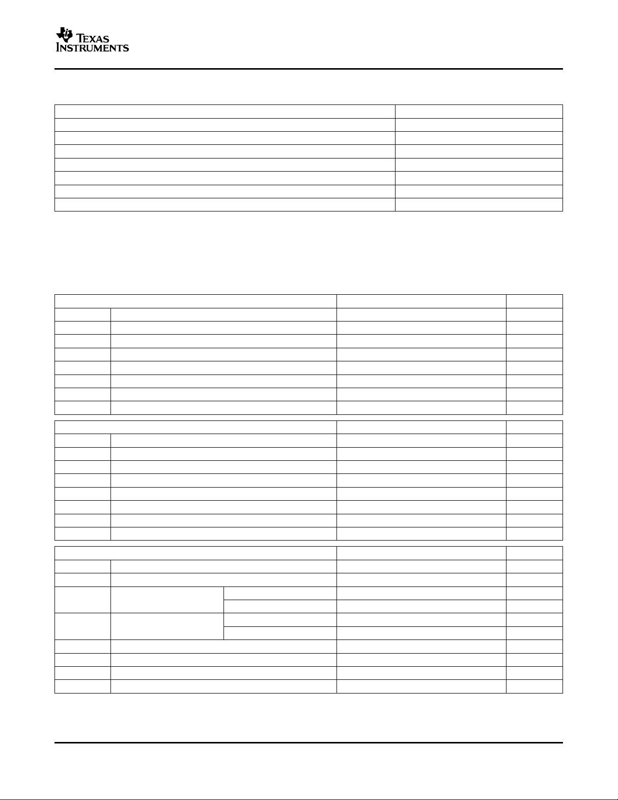
ABSOLUTE MAXIMUM RATINGS
(1)
over operating free-air temperature range (unless otherwise noted)
UNIT
Supply voltage range, V
Input voltage range at any input, V
Output voltage range, V
O
(2)
(see
CC
) -0.5 V to 7 V
I
-0.5 V to 7 V
-0.5 V to 7 V
Operating free-air temperature, TA, TL16C2550 0°C to 70°C
Operating free-air temperature, TA, TL16C2550I -40°C to 85°C
Storage temperature range, T
stg
-65°C to 150°C
Lead temperature 1,6 mm (1/16 inch) from case for 10 seconds 260°C
(1) Stresses beyond those listed under "absolute maximum ratings" may cause permanent damage to the device. These are stress ratings
only, and functional operation of the device at these or any other conditions beyond those indicated under "recommended operating
conditions" is not implied. Exposure to absolute-maximum-rated conditions for extended periods may affect device reliability.
(2) All voltage values are with respect to VSS.
RECOMMENDED OPERATING CONDITIONS
over operating free-air temperature range (unless otherwise noted)
2.5 V ±10% MIN NOM MAX UNIT
V
CC
V
I
V
IH
V
IL
V
O
I
OH
I
OL
Supply voltage 2.25 2.5 2.75 V
Input voltage 0 V
CC
High-level input voltage 1.8 2.75 V
Low-level input voltage -0.3 0.6 V
Output voltage 0 V
CC
High-level output current (all outputs) 1 mA
Low-level output current (all outputs) 2 mA
Oscillator/clock speed 16 MHz
TL16C2550
V
V
3.3 V ±10% MIN NOM MAX UNIT
V
CC
V
I
V
IH
V
IL
V
O
I
OH
I
OL
Supply voltage 3 3.3 3.6 V
Input voltage 0 V
High-level input voltage 0.7V
CC
Low-level input voltage 0.3V
Output voltage 0 V
CC
CC
CC
High-level output current (all outputs) 1.8 mA
Low-level output current (all outputs) 3.2 mA
Oscillator/clock speed 20 MHz
5 V ±10% MIN NOM MAX UNIT
V
CC
V
I
V
IH
V
IL
V
O
I
OH
I
OL
Supply voltage 4.5 5 5.5 V
Input voltage 0 V
CC
High-level input voltage All except XTAL1, XTAL2 2 V
XTAL1, XTAL2 0.7V
CC
Low-level input voltage All except XTAL1, XTAL2 0.8 V
XTAL1, XTAL2 0.3V
Output voltage 0 V
CC
CC
High-level output current (all outputs) 4 mA
Low-level output current (all outputs) 4 mA
Oscillator/clock speed 24 MHz
V
V
V
V
V
V
9
Page 10
www.ti.com
PRODUCT PREVIEW
TL16C2550
SLWS161 – JUNE 2005
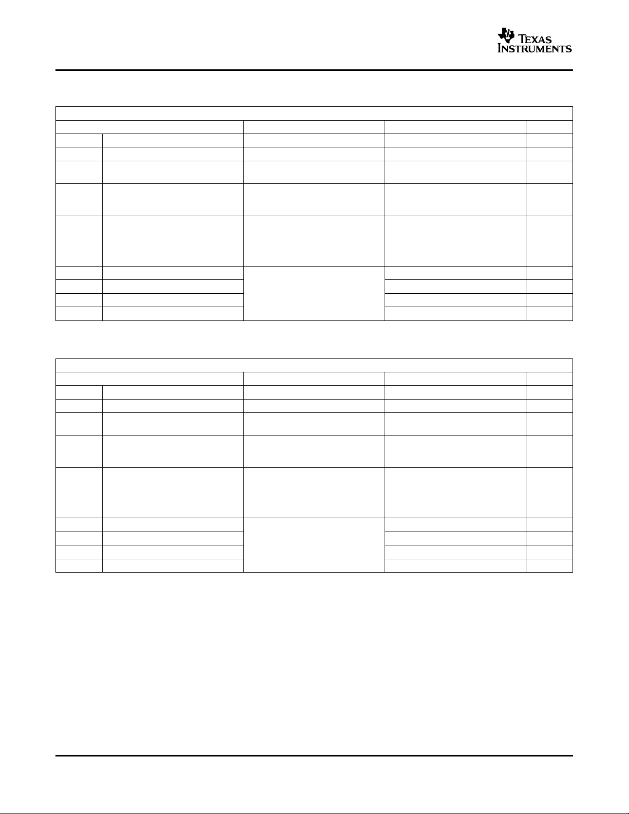
ELECTRICAL CHARACTERISTICS
over recommended ranges of supply voltage and operating free-air temperature (unless otherwise noted)
2.5 V Nominal
PARAMETER TEST CONDITIONS MIN TYP
V
OH
V
OL
I
I
I
OZ
I
CC
C
i(CLK)
C
O(CLK)
C
I
C
O
High-level output voltage
Low-level output voltage
Input current V
High-impedance-state output current V
Supply current V
Clock input impedance V
Clock output impedance 20 30 pF
Input impedance 6 10 pF
Output impedance 10 20 pF
(1) All typical values are at V
(2) These parameters apply for all outputs except XTAL2.
ADDED SPACE
3.3V Nominal
PARAMETER TEST CONDITIONS MIN TYP
V
OH
V
OL
I
I
I
OZ
I
CC
C
i(CLK)
C
O(CLK)
C
I
C
O
High-level output voltage
Low-level output voltage
Input current V
High-impedance-state output current V
Supply current V
Clock input impedance V
Clock output impedance 20 30 pF
Input impedance 6 10 pF
Output impedance 10 20 pF
(1) All typical values are at V
(2) These parameters apply for all outputs except XTAL2.
(2)
(2)
= 2.5 V and TA= 25°C.
CC
(2)
(2)
= 3.3 V and TA= 25°C.
CC
IOH= -1 mA 1.8 V
IOL= 2 mA 0.5 V
= 3.6 V, V
CC
V, All other terminals floating
= 3.6 V, V
CC
V, Chip slected in write mode or chip
= 0, VI= 0 to 3.6 10 µA
SS
= 0, VI= 0 to 3.6 ±20 µA
SS
deselcted
= 3.6 V, TA= 25°C, RXA, RXB, 16 mA
CC
DSRA, DSRB, CDA, CDB, CTSA,
CTSB, RIA, and RIB at 2 V, All other
inputs at 0.8 V, XTAL1 at 4 MHz, No
load on outputs,
= 0, V
CC
25°C, All other terminals grounded
= 0, f = 1 MHz, TA= 15 20 pF
SS
IOH= -1.8 mA 2.4 V
IOL= 3.2 mA 0.5 V
= 3.6 V, V
CC
V, All other terminals floating
= 3.6 V, V
CC
V, Chip slected in write mode or chip
= 0, VI= 0 to 3.6 10 µA
SS
= 0, VI= 0 to 3.6 ±20 µA
SS
deselcted
= 3.6 V, TA= 25°C, RXA, RXB, 20 mA
CC
DSRA, DSRB, CDA, CDB, CTSA,
CTSB, RIA, and RIB at 2 V, All other
inputs at 0.8 V, XTAL1 at 4 MHz, No
load on outputs,
= 0, V
CC
25°C, All other terminals grounded
= 0, f = 1 MHz, TA= 15 20 pF
SS
(1)
(1)
MAX UNIT
MAX UNIT
10
Page 11
www.ti.com
5 V Nomial
PARAMETER TEST CONDITIONS MIN TYP
V
OH
V
OL
I
I
I
OZ
High-level output voltage
Low-level output voltage
Input current V
High-impedance-state output current V
(2)
(2)
IOH= -4 mA 4 V
IOL= 4 mA 0.4 V
= 5.25 V, V
CC
V, All other terminals floating
= 5.25 V, V
CC
V, Chip slected in write mode or chip
= 0, VI= 0 to 5.25 10 µA
SS
= 0, VI= 0 to 5.25 ±20 µA
SS
(1)
deselcted
I
CC
Supply current V
= 5.25 V, TA= 25°C, RXA, 24 mA
CC
RXB, DSRA, DSRB, CDA, CDB,
CTSA, CTSB, RIA, and RIB at 2 V,
All other inputs at 0.8 V, XTAL1 at 4
MHz, No load on outputs,
C
i(CLK)
C
O(CLK)
C
I
C
O
(1) All typical values are at V
(2) These parameters apply for all outputs except XTAL2.
Clock input impedance V
Clock output impedance 20 30 pF
= 0, V
CC
25°C, All other terminals grounded
SS
= 0, f = 1 MHz, TA= 15 20 pF
Input impedance 6 10 pF
Output impedance 10 20 pF
= 5 V and TA= 25°C.
CC
TIMING REQUIREMENTS
over recommended ranges of supply voltage and operating free-air temperature (unless otherwise noted)
PARAMETER 2.5 V 3.3 V 5 V UNIT
ALT. SYM- FIG- TEST
BOL URE CONDITIONS
MIN MAX MIN MAX MIN MAX
t
Cycle time, read (tw7+ td8+ td9) RC 87 ns
cR
t
Cycle time, write (tw6+ td5+ td6) WC 87 ns
cW
t
Pulse duration, clock high t
w1
t
Pulse duration, clock low t
w2
t
Pulse duration, clock high t
w1
t
Pulse duration, clock low t
w2
t
Pulse duration, clock high t
w1
t
Pulse duration, clock low t
w2
t
Pulse duration, IOW t
w6
t
Pulse duration, IOR t
w7
t
Pulse duration, RESET t
w8
t
Setup time, data valid before IOW↑ t
SU3
t
Setup time, CTS↑ before midpoint of 17 10 ns
SU4
stop bit
t
Hold time, CS valid after IOW↑ t
h3
t
Hold time, address valid after IOW↑ t
h4
t
Hold time, data valid after IOW↑ t
h5
t
Hold time, chip select valid after IOR↑ t
h6
t
Hold time, address valid after IOR↑ t
h7
t
Delay time, CS valid before IOW↓ t
d4
t
Delay time, address valid before t
d5
IOW↓
t
Delay time, CS valid to IOR↓ t
d7
t
Delay time, address valid to IOR↓ t
d8
t
Delay time, IOR↓ to data valid t
d10
t
Delay time, IOR↑ to floating data t
d11
XH
XL
XH
XL
XH
XL
IOW
IOR
RESET
DS
WCS
WA
DH
RCS
RA
CSW
AW
CSR
AR
RVD
HZ
5 f = 16 MHz Max, 25 ns
V
= 2.5 V
CC
5 f = 20 MHz Max, 20 ns
V
= 3.3 V
CC
5 f = 24 MHz Max, 18 ns
V
= 5 V
CC
6 40 ns
7 40 ns
1 µs
6 15 ns
6 10 ns
6 5 ns
7 10 ns
7 20 ns
6 7 ns
7 7 ns
7 CL= 75 pF 45 ns
7 CL= 75 pF 20 ns
LIMITS
TL16C2550
SLWS161 – JUNE 2005
MAX UNIT
11
Page 12

www.ti.com
PRODUCT PREVIEW
TL16C2550
SLWS161 – JUNE 2005
RECEIVER SWITCHING CHARACTERISTICS
over recommended ranges of supply voltage and operating free-air temperature (unless otherwise noted) (see
PARAMETER 2.5 V 3.3 V 5 V UNIT
ALT. SYM- FIG- TEST
BOL URE CONDITIONS
MIN MAX MIN MAX MIN MAX
t
Delay time, RCLK to sample t
d12
t
Delay time, stop to set INT or read t
d13
RBR to LSI interrupt or stop to 10, 11, cycle
SCD
SINT
8 10 ns
8, 9, 1 RCLK
RXRDY↓ 12
t
Delay time, read RBR/LSR to reset t
d14
INT 10, 11,
RINT
8, 9, CL= 75 pF 70 ns
12
(1) In the FIFO mode, the read cycle (RC) = 425 ns (min) between reads of the receive FIFO and the status registers (interrupt identification
register or line status register).
TRANSMITTER SWITCHING CHARACTERISTICS
over recommended ranges of supply voltage and operating free-air temperature (unless otherwise noted)
PARAMETER 2.5 V 3.3 V 5 V UNIT
t
Delay time, initial write to transmit t
d15
start cycles
t
Delay time, start to INT t
d16
t
Delay time, IOW (WR THR) to reset t
d17
INT
t
Delay time, initial write to INT t
d18
t
d19
t
d20
t
d21
(1)
(THRE
Delay time, read IOR↑ to reset INT t
(THRE
) cycles
(1)
)
Delay time, write to TXRDY inactive t
Delay time, start to TXRDY active t
(1) THRE = transmitter holding register empty; IIR = interrupt identification register.
ALT. SYM- FIG- TEST
BOL URE CONDITIONS
IRS
STI
HR
SI
IR
WXI
SXA
13 8 24 baudout
13 8 10 baudout
13 CL= 75 pF 50 ns
13 16 34 baudout
13 CL= 75 pF 35 ns
14, 15 CL= 75 pF 35 ns
14, 15 CL= 75 pF 9 baudout
MIN MAX MIN MAX MIN MAX
LIMITS
LIMITS
(1)
)
cycles
cycles
12
Page 13
www.ti.com
MODEM CONTROL SWITCHING CHARACTERISTICS
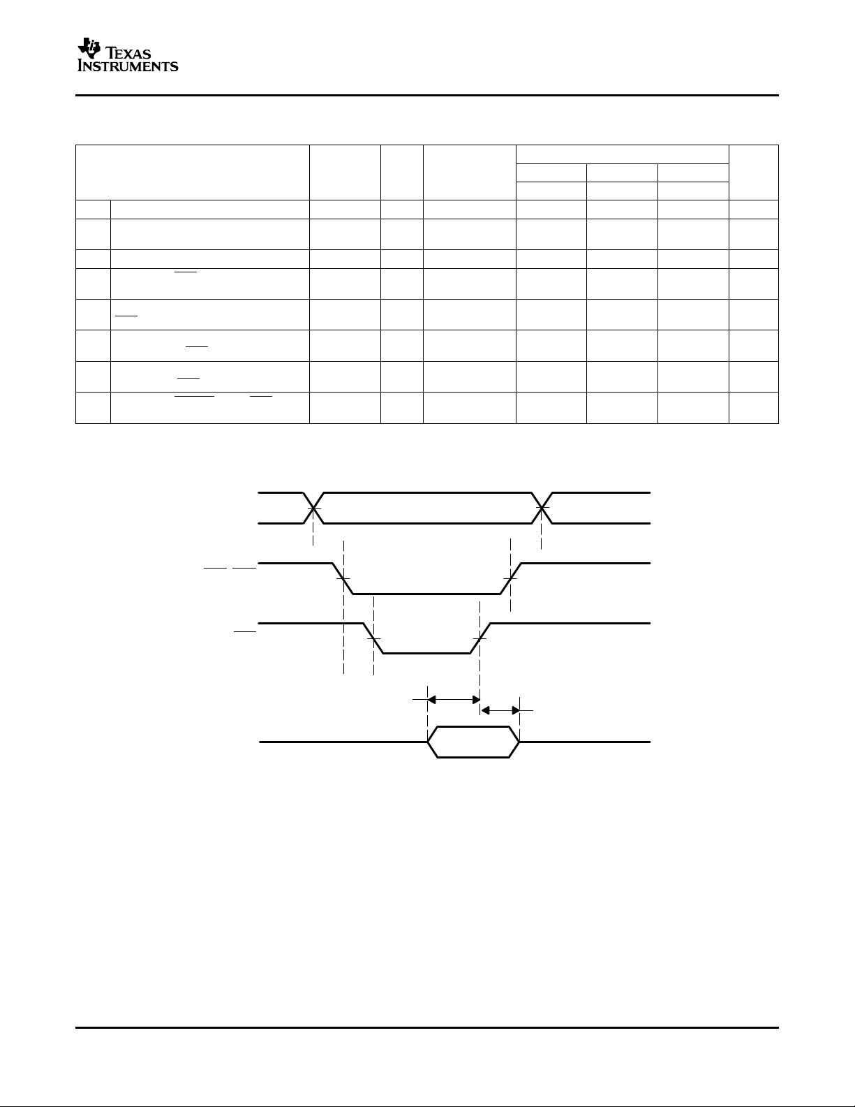
t
su3
t
h5
Valid Data
Valid
A2−A0
D7−D0
50%50%
50%
50%
50%50%
IOW
CSA, CSB
over operating free-air temperature range (unless otherwise noted)
PARAMETER 2.5 V 3.3 V 5 V UNIT
ALT. SYM- FIG- TEST
BOL URE CONDITIONS
MIN MAX MIN MAX MIN MAX
t
Delay time, WR MCR to output t
d22
t
Delay time, modem interrupt to set t
d23
INT
t
Delay time, RD MSR to reset INT t
d24
t
Delay time, CTS low to TX ↓ 17 CL= 75 pF baudout
d25
t
Delay time, RCV threshold byte to 18 CL= 75 pF baudout
d26
RTS↑ cycles
t
Delay time, read of last byte in re- 18 CL= 75 pF baudout
d27
ceive FIFO to RTS↓ cycles
t
Delay time, first data bit of 16th 19 CL= 75 pF baudout
d28
character to RTS↑ cycles
t
Delay time, RBRRD low to RTS↓ 19 CL= 75 pF baudout
d29
MDO
SIM
RIM
16 CL= 75 pF ns
16 CL= 75 pF ns
16 CL= 75 pF ns
(1) A baudout cycle is equal to the period of the input clock divided by the programmed divider in DLL, DLM.
LIMITS
TL16C2550
SLWS161 – JUNE 2005
(1)
cycles
cycles
Figure 7. Write Cycle Timing Waveforms
13
Page 14

www.ti.com
PRODUCT PREVIEW
t
d10
t
d11
Valid Data
Valid
A2−A0
D7−D0
50%50%
50%
50%
50%50%
IOR
CSA, CSB
t
d13
Active
Active
IOR
(read RBR)
RCLK
(Internal)
t
d14
t
d14
t
d12
Parity StopStart Data Bits 5−8
Sample Clock
(Internal)
TL16C450 Mode:
Sample Clock
RXA, RXB
INT
(data ready)
INT
(RCV error)
IOR
(read LSR)
50%50%
50%
50%
50%
50%
8 CLKs
TL16C2550
SLWS161 – JUNE 2005
Figure 8. Read Cycle Timing Waveforms
Figure 9. Receiver Timing Waveforms
14
Page 15

www.ti.com
t
d13
(see Note A)
t
d14
Stop
Data Bits 5−8
Sample Clock
(Internal)
RXA, RXB
Trigger Level
INT
(FCR6, 7 = 0, 0)
INT
Line Status
Interrupt (LSI)
t
d14
IOR
(RD LSR)
IOR
(RD RBR)
Active
Active
(FIFO at or above
trigger level)
(FIFO below
trigger level)
50%50%
50%
50%
50%
50%
t
d13
(see Note A)
t
d14
Stop
Top Byte of FIFO
Sample Clock
(Internal)
RXA, RXB
Time-Out or
Trigger Level
Interrupt
Line Status
Interrupt (LSI)
t
d13
(FIFO at or above
trigger level)
(FIFO below
trigger level)
IOP
(RD LSR)
IOR
(RD RBR)
Active Active
t
d14
Previous Byte
Read From FIFO
50%
50%
50%50%
50%
50% 50%
TL16C2550
SLWS161 – JUNE 2005
Figure 10. Receive FIFO First Byte (Sets DR Bit) Waveforms
Figure 11. Receive FIFO Bytes Other Than the First Byte (DR Internal Bit Already Set) Waveforms
15
Page 16
www.ti.com
PRODUCT PREVIEW
t
d13
(see Note B)
t
d14
Stop
Sample Clock
(Internal)
RXA, RXB
(first byte)
Active
IOR
(RD RBR)
RXRDYA
, RXRDYB
See Note A
50%
50%
50%
t
d13
(see Note B)
t
d14
Sample Clock
(Internal)
RXA, RXB
(first byte that reaches
the trigger level)
Active
IOR
(RD RBR)
RXRDYA
, RXRDYB
See Note A
50%
50%50%
t
d16
Parity Stop
Start
Data Bits
TXA, TXB
Start
t
d15
t
d17
t
d17
t
d18
t
d19
INT
(THRE)
IOW
(WR THR)
IOR
50% 50% 50% 50% 50%
50%
50%
50%
50%
50%
50%
TL16C2550
SLWS161 – JUNE 2005
Figure 12. Receiver Ready ( RXRDY) Waveforms, FCR0 = 0 or FCR0 = 1 and FCR3 = 0 (Mode 0)
Figure 13. Receiver Ready ( RXRDY) Waveforms, FCR0 = 1 and FCR3 = 1 (Mode 1)
16
Figure 14. Transmitter Timing Waveforms
Page 17

www.ti.com
t
d20
IOW
(WR THR)
t
d21
Parity
Stop
Data
Start
Byte 1
TXA, TXB
TXRDYA, TXRDYB
50%
50%
50%
50%
IOW
(WR THR)
Parity
Stop
Data
Start
Byte 16
TXA, TXB
TXRDYA, TXRDYB
FIFO Full
t
d20
t
d21
50%
50%
50%
50%
IOW
(WR MCR)
RTSA, RTSB, DTRA,
DTRB, OPA, OPB
CTSA, CTSB, DSRA,
DSRB, CDA, CDB
t
d23
t
d24
t
d23
INT
(modem)
IOR
(RD MSR)
RI
50% 50%
50% 50%
50%
50%
50%
50%
50%
50%
t
d22
t
d22
TL16C2550
SLWS161 – JUNE 2005
Figure 15. Transmitter Ready ( TXRDY) Waveforms, FCR0 = 0 or FCR0 = 1 and FCR3 = 0 (Mode 0)
Figure 16. Transmitter Ready ( TXRDY) Waveforms, FCR0 = 1 and FCR3 = 1 (Mode 1)
Figure 17. Modem Control Timing Waveforms
17
Page 18

www.ti.com
PRODUCT PREVIEW
Midpoint of Stop Bit
t
d25
t
su4
CTSA, CTSB
TXA, TXB
50% 50%
50%
t
d27
RXA, RXB
50%
t
d26
50%
50%
Midpoint of Stop Bit
RTSA
,
RTSB
IOR
RXA,
RXB
50%
t
d28
50%
50%
Midpoint of Data Bit 0
RTSA
,
RTSB
IOR
15th Character 16th Character
t
d29
TL16C2550
SLWS161 – JUNE 2005
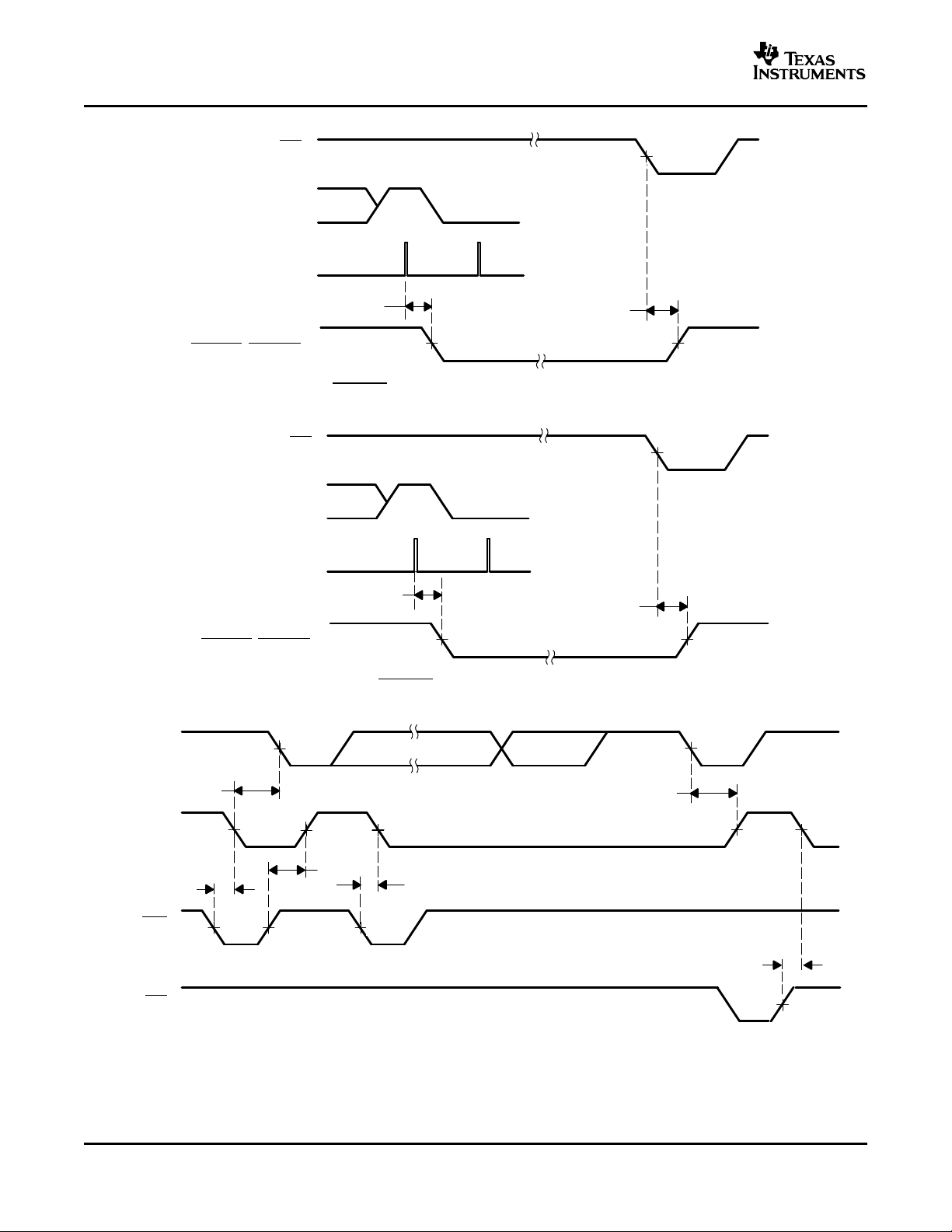
Figure 18. CTS and TX Autoflow Control Timing (Start and Stop) Waveforms
Figure 19. Auto- RTS Timing for RCV Threshold of 1, 4, or 8 Waveforms
Figure 20. Auto- RTS Timing for RCV Threshold of 14 Waveforms
18
Page 19

www.ti.com
D7−D0
MEMR or I/OR
MEMW or I/OW
INTR
RESET
A0
A1
A2
CS
EIA-232-D
Drivers
and Receivers
XTAL2
XTAL1
RIA, B
CTSA, B
CDA, B
DSRA, B
DTRA, B
RTSA, B
TXA, B
RXA, B
INTA, B
D7−D0
IOR
IOW
RESET
A0
A1
A2
CSA
, B
TL16C2550
3.072 MHz
C
P
U
B
u
s
(Optional)
TL16C2550
SLWS161 – JUNE 2005
APPLICATION INFORMATION
Figure 21. Basic TL16C2550 Configuration
19
Page 20

www.ti.com
PRODUCT PREVIEW
Buffer
(Optional)
Address
Decoder
A0−A23
D0−D15
RSI/ABT
PHI1 PHI2
PHI1 PHI2
CPU
RSTO
A0−A2
CSA
CSB
RESET
D0−D7
D0−D7
IOR
IOW
XTAL1
XTAL2
DTRA, B
RTSA, B
RIA, B
CDA, B
DSRA, B
CTSA, B
RXA, B
TXA, B
INTA, B
GND
(VSS)
V
CC
17
42
Alternate
Crystal Control
TL16C2550
EIA-232-D
Connector
20
1
8
6
5
2
3
7
1
14
15
34, 35
33, 22
41, 21
40, 16
39, 20
38, 23
5, 4
30, 29
7, 8
15
19
36
10
11
TCU
WR
RD
(Optional)
TL16C2550
SLWS161 – JUNE 2005
APPLICATION INFORMATION (continued)
A. Pin numbers shown are for 48-pin TQFP PFB package.
20
Figure 22. Typical TL16C2550 Connection
Page 21

www.ti.com
TL16C2550
SLWS161 – JUNE 2005
PRINCIPLES OF OPERATION
Register Selection
Table 1. Register Selection
(1)
DLAB
0 L L L Receiver buffer (read), transmitter holding register (write)
0 L L H Interrupt enable register
X L H L Interrupt identification register (read only)
X L H L FIFO control register (write)
X L H H Line control register
X H L L Modem control register
X H L H Line status register
X H H L Modem status register
X H H H Scratch register
1 L L L Divisor latch (LSB)
1 L L H Divisor latch (MSB)
(1) The divisor latch access bit (DLAB) is the most significant bit of the line control register. The DLAB signal is controlled by writing to this
bit location (see Table 4).
A2 A1 A0 REGISTER
Table 2. ACE Reset Functions
REGISTER/SIGNAL RESET CONTROL RESET STATE
Interrupt enable register Master reset All bits cleared (0 - 3 forced and 4 - 7 permanent)
Interrupt identification register Master reset Bit 0 is set, bits 1, 2, 3, 6, and 7 are cleared, and bits
FIFO control register Master reset All bits cleared
Line control register Master reset All bits cleared
Modem control register Master reset All bits cleared (6 - 7 permanent)
Line status register Master reset Bits 5 and 6 are set; all other bits are cleared
Modem status register Master reset Bits 0 - 3 are cleared; bits 4 - 7 are input signals
TX Master reset High
INTRPT (receiver error flag) Read LSR/MR Low
INTRPT (received data available) Read RBR/MR Low
INTRPT (transmitter holding register empty) Read IR/write THR/MR Low
INTRPT (modem status changes) Read MSR/MR Low
OP Master reset High
RTS Master reset High
DTR Master reset High
Scratch register Master reset No effect
Divisor latch (LSB and MSB) registers Master reset No effect
Receiver buffer register Master reset No effect
Transmitter holding register Master reset No effect
RCVR FIFO MR/FCR1 - FCR0/DFCR0 All bits cleared
XMIT FIFO MR/FCR2 - FCR0/DFCR0 All bits cleared
4 - 5 are permanently cleared
Accessible Registers
The system programmer, using the CPU, has access to and control over any of the ACE registers that are
summarized in Table 2. These registers control ACE operations, receive data, and transmit data. Descriptions of
these registers follow Table 3.
21
Page 22

www.ti.com
PRODUCT PREVIEW
TL16C2550
SLWS161 – JUNE 2005
Table 3. Summary of Accessible Registers
BIT REGISTER ADDRESS
NO.
0 0 1 2 2 3 4 5 6 7 0 1
Receiver Transmitter Interrupt Interrupt FIFO Con- Line Con- Modem Line Status Modem Scratch Divisor Divisor
Buffer Holding Enable Ident trol Regis- trol Regis- Control Register Status Register Latch (LSB) Latch
Register Register Register .Register ter ter Register Register (MSB)
(Read Only) (Write Only) (Read Only) (WriteOnly)
RBR THR IER IIR FCR LCR MCR LSR MSR SCR DLL DLM
0 Data Bit 0
1 Data Bit 1 Data Bit 1 Enable Interrupt ID Receiver Word Request to Overrun Er- Delta Data Bit 1 Bit 1 Bit 9
2 Data Bit 2 Data Bit 2 Enable Re- Interrupt ID Transmitter Number of OUT1 Parity Error Trailing Bit 2 Bit 2 Bit 10
3 Data Bit 3 Data Bit 3 Enable Interrupt ID DMA Mode Parity En- OUT2 Framing Er- Delta Data Bit 3 Bit 3 Bit 11
4 Data Bit 4 Data Bit 4 0 0 Reserved Even Parity Loop Break Inter- Clear to Bit 4 Bit 4 Bit 12
5 Data Bit 5 Data Bit 5 0 0 Reserved Stick Parity Autoflow Transmitter Data Set Bit 5 Bit 5 Bit 13
6 Data Bit 6 Data Bit 6 0 FIFOs En- Receiver Break Con- 0 Transmitter Ring Indi- Bit 6 Bit 6 Bit 14
7 Data Bit 7 Data Bit 7 0 FIFOs En- Receiver Divisor 0 Error in Data Carrier Bit 7 Bit 7 Bit 15
(1)
Data Bit 0 Enable Re- 0 if Interrupt FIFO Enable Word Data Ter- Data Ready Delta Clear Bit 0 Bit 0 Bit 8
ceived Data Pending Length Sel- minal Ready (DR) to Send
Available In- ect Bit 0 (DTR) ( ∆ CTS)
terrupt (WLS0)
(ERBI)
Transmitter Bit 1 FIFO Reset Length Sel- Send (RTS) ror (OE) Set Ready
Holding ect Bit 1 ( ∆ DSR)
Register (WLS1)
Empty Interrupt (ETBEI)
ceiver Line Bit 2 FIFO Reset Stop Bits (PE) Edge Ring
Status Inter- (STB) Indicator
rupt (ELSI) (TERI)
Modem Bit 3
Status Inter- tect ( ∆ DCD)
rupt (EDSSI)
(2)
(2)
abled
(2)
abled
(1) Bit 0 is the least significant bit. It is the first bit serially transmitted or received.
(2) These bits are always 0 in the TL16C450 mode.
DLAB = 0 DLAB = 1
Select able (PEN) ror (FE) Carrier De-
Select rupt (BI) Send (CTS)
(EPS)
Control En- Holding Ready
able (AFE) Register (DSR)
Trigger trol Empty cator (RI)
(LSB) (TEMT)
Trigger Latch Ac- RCVR Detect
(MSB) cess Bit FIFO
(DLAB)
(THRE)
(2)
(DCD)
FIFO Control Register (FCR)
The FCR is a write-only register at the same location as the IIR, which is a read-only register. The FCR enables
and clears the FIFOs, sets the receiver FIFO trigger level, and selects the type of DMA signalling.
• Bit 0: This bit, when set, enables the transmitter and receiver FIFOs. Bit 0 must be set when other FCR bits
are written to or they are not programmed. Changing this bit clears the FIFOs.
• Bit 1: This bit, when set, clears all bytes in the receiver FIFO and clears its counter. The shift register is not
cleared. The 1 that is written to this bit position is self-clearing.
• Bit 2: This bit, when set, clears all bytes in the transmit FIFO and clears its counter. The shift register is not
cleared. The 1 that is written to this bit position is self-clearing.
• Bit 3: When FCR0 is set, setting FCR3 causes RXRDY and TXRDY to change from level 0 to level 1.
• Bits 4 and 5: These two bits are reserved for future use.
• Bits 6 and 7: These two bits set the trigger level for the receiver FIFO interrupt (see Table 4).
BIT 7 BIT 6 RECEIVER FIFOTRIGGER LEVEL (BYTES)
0 0 01
0 1 04
1 0 08
1 1 14
22
Table 4. Receiver FIFO Trigger Level
Page 23

www.ti.com
TL16C2550
SLWS161 – JUNE 2005
FIFO Interrupt Mode Operation
When the receiver FIFO and receiver interrupts are enabled (FCR0 = 1, IER0 = 1, IER2 = 1), a receiver interrupt
occurs as follows:
1. The received data available interrupt is issued to the microprocessor when the FIFO has reached its
programmed trigger level. It is cleared when the FIFO drops below its programmed trigger level.
2. The IIR receive data available indication also occurs when the FIFO trigger level is reached, and like the
interrupt, it is cleared when the FIFO drops below the trigger level.
3. The receiver line status interrupt (IIR = 06) has higher priority than the received data available (IIR = 04)
interrupt.
4. The data ready bit (LSR0) is set when a character is transferred from the shift register to the receiver FIFO. It
is cleared when the FIFO is empty.
When the receiver FIFO and receiver interrupts are enabled:
1. FIFO time-out interrupt occurs if the following conditions exist:
a. At least one character is in the FIFO.
b. The most recent serial character was received more than four continuous character times ago (if two
stop bits are programmed, the second one is included in this time delay).
c. The most recent microprocessor read of the FIFO has occurred more than four continuous character
times before. This causes a maximum character received command to interrupt an issued delay of 160
ms at a 300-baud rate with a 12-bit character.
2. Character times are calculated by using the RCLK input for a clock signal (makes the delay proportional to
the baud rate).
3. When a time-out interrupt has occurred, it is cleared and the timer is cleared when the microprocessor reads
one character from the receiver FIFO.
4. When a time-out interrupt has not occurred, the time-out timer is cleared after a new character is received or
after the microprocessor reads the receiver FIFO.
When the transmitter FIFO and THRE interrupt are enabled (FCR0 = 1, IER1 = 1), transmit interrupts occur as
follows:
1. The transmitter holding register empty interrupt [IIR (3 -0) = 2] occurs when the transmit FIFO is empty. It is
cleared [IIR (3 -0) = 1] when the THR is written to (1 to 16 characters may be written to the transmit FIFO
while servicing this interrupt) or the IIR is read.
2. The transmitter holding register empty interrupt is delayed one character time minus the last stop bit time
when there have not been at least two bytes in the transmitter FIFO at the same time since the last time that
the FIFO was empty. The first transmitter interrupt after changing FCR0 is immediate if it is enabled.
FIFO Polled Mode Operation
With FCR0 = 1 (transmitter and receiver FIFOs enabled), clearing IER0, IER1, IER2, IER3, or all four to 0 puts
the ACE in the FIFO polled mode of operation. Because the receiver and transmitter are controlled separately,
either one or both can be in the polled mode of operation.
In this mode, the user program checks receiver and transmitter status using the LSR. As stated previously:
• LSR0 is set as long as one byte is in the receiver FIFO.
• LSR1 - LSR 4 specify which error(s) have occurred. Character error status is handled the same way as when
in the interrupt mode; the IIR is not affected since IER2 = 0.
• LSR5 indicates when the THR is empty.
• LSR6 indicates that both the THR and TSR are empty.
• LSR7 indicates whether any errors are in the receiver FIFO.
There is no trigger level reached or time-out condition indicated in the FIFO polled mode. However, the
receiver and transmitter FIFOs are still fully capable of holding characters.
23
Page 24

www.ti.com
PRODUCT PREVIEW
TL16C2550
SLWS161 – JUNE 2005
Interrupt Enable Register (IER)
The IER enables each of the five types of interrupts (see Table 5) and enables INTRPT in response to an
interrupt generation. The IER can also disable the interrupt system by clearing bits 0 through 3. The contents of
this register are summarized in Table 3 and are described in the following bullets.
• Bit 0: When set, this bit enables the received data available interrupt.
• Bit 1: When set, this bit enables the THRE interrupt.
• Bit 2: When set, this bit enables the receiver line status interrupt.
• Bit 3: When set, this bit enables the modem status interrupt.
• Bits 4 through 7: These bits are not used (always cleared).
Interrupt Identification Register (IIR)
The ACE has an on-chip interrupt generation and prioritization capability that permits a flexible interface with the
most popular microprocessors.
The ACE provides four prioritized levels of interrupts:
• Priority 1 - Receiver line status (highest priority)
• Priority 2 - Receiver data ready or receiver character time-out
• Priority 3 - Transmitter holding register empty
• Priority 4 - Modem status (lowest priority)
When an interrupt is generated, the IIR indicates that an interrupt is pending and encodes the type of interrupt in
its three least significant bits (bits 0, 1, and 2). The contents of this register are summarized in Table 3 and
described in Table 5. Detail on each bit is as follows:
• Bit 0: This bit is used either in a hardwire prioritized or polled interrupt system. When bit 0 is cleared, an
interrupt is pending. If bit 0 is set, no interrupt is pending.
• Bits 1 and 2: These two bits identify the highest priority interrupt pending as indicated in Table 3
• Bit 3: This bit is always cleared in TL16C450 mode. In FIFO mode, bit 3 is set with bit 2 to indicate that a
time-out interrupt is pending.
• Bits 4 and 5: These two bits are not used (always cleared).
• Bits 6 and 7: These bits are always cleared in TL16C450 mode. They are set when bit 0 of the FIFO control
register is set.
INTERRUPT IDENTIFICATION PRIORITY INTERRUPT TYPE INTERRUPT SOURCE NTERRUPT RESET
BIT 3 BIT 2 BIT 1 BIT 0
0 0 0 1 None None None None
0 1 1 0 1 Receiver line status Overrun error, parity er- Read the line status regis-
0 1 0 0 2 Received data available Receiver data available in Read the receiver buffer
1 1 0 0 2 Character time-out indi- No characters have been Read the receiver buffer
0 0 1 0 3 Transmitter holding regis- Transmitter holding regis- Read the interrupt identifi-
24
REGISTER LEVEL METHOD
Table 5. Interrupt Control Functions
ror, framing error, or ter
break interrupt
the TL16C450 mode or register
trigger level reached in
the FIFO mode
cation removed from or input to register
the receiver FIFO during
the last four character
times, and there is at
least one character in it
during this time
ter empty ter empty cation register (if source
of interrupt) or writing into
the transmitter holding
register
Page 25

www.ti.com
TL16C2550
SLWS161 – JUNE 2005
Table 5. Interrupt Control Functions (continued)
INTERRUPT IDENTIFICATION PRIORITY INTERRUPT TYPE INTERRUPT SOURCE NTERRUPT RESET
BIT 3 BIT 2 BIT 1 BIT 0
0 0 0 0 4 Modem status Clear to send, data set Read the modem status
Line Control Register (LCR)
The system programmer controls the format of the asynchronous data communication exchange through the
LCR. In addition, the programmer is able to retrieve, inspect, and modify the contents of the LCR; this eliminates
the need for separate storage of the line characteristics in system memory. The contents of this register are
summarized in Table 3 and described in the following bulleted list.
• Bits 0 and 1: These two bits specify the number of bits in each transmitted or received serial character.
These bits are encoded as shown in Table 6 .
• Bit 2: This bit specifies either one, one and one-half, or two stop bits in each transmitted character. When bit
2 is cleared, one stop bit is generated in the data. When bit 2 is set, the number of stop bits generated is
dependent on the word length selected with bits 0 and 1. The receiver clocks only the first stop bit regardless
of the number of stop bits selected. The number of stop bits generated in relation to word length and bit 2 are
shown in Table 7 .
REGISTER LEVEL METHOD
ready, ring indicator, or register
data carrier detect
Table 6. Serial Character Word Length
BIT 1 BIT 0 WORD LENGTH
0 0 5 bits
0 1 6 bits
1 0 7 bits
1 1 8 bits
Table 7. Number of Stop Bits Generated
BIT 2 Word Length Selectedby Bits 1 and 2 Number of StopBits Generated
0 Any word length 1
1 5 bits 1 1/2
1 6 bits 2
1 7 bits 2
1 8 bits 2
• Bit 3: This bit is the parity enable bit. When bit 3 is set, a parity bit is generated in transmitted data between
the last data word bit and the first stop bit. In received data, if bit 3 is set, parity is checked. When bit 3 is
cleared, no parity is generated or checked.
• Bit 4: This bit is the even parity select bit. When parity is enabled (bit 3 is set) and bit 4 is set, even parity (an
even number of logic 1s in the data and parity bits) is selected. When parity is enabled and bit 4 is cleared,
odd parity (an odd number of logic 1s) is selected.
• Bit 5: This bit is the stick parity bit. When bits 3, 4, and 5 are set, the parity bit is transmitted and checked as
cleared. When bits 3 and 5 are set and bit 4 is cleared, the parity bit is transmitted and checked as set. If bit
5 is cleared, stick parity is disabled.
• Bit 6: This bit is the break control bit. Bit 6 is set to force a break condition; i.e., a condition where TX is
forced to the spacing (cleared) state. When bit 6 is cleared, the break condition is disabled and has no effect
on the transmitter logic; it only effects TX.
• Bit 7: This bit is the divisor latch access bit (DLAB). Bit 7 must be set to access the divisor latches of the
baud generator during a read or write. Bit 7 must be cleared during a read or write to access the receiver
buffer, the THR, or the IER.
25
Page 26

www.ti.com
PRODUCT PREVIEW
TL16C2550
SLWS161 – JUNE 2005
Line Status Register (LSR)
The line status register is intended for read operations only; writing to this register is
not recommended outside of a factory testing environment.
The LSR provides information to the CPU concerning the status of data transfers. The contents of this register
are summarized in Table 3 and described in the following bulleted list.
• Bit 0: This bit is the data ready (DR) indicator for the receiver. DR is set whenever a complete incoming
character has been received and transferred into the RBR or the FIFO. DR is cleared by reading all of the
data in the RBR or the FIFO.
Bits 1 through 4 are the error conditions that produce a receiver line status interrupt.
• Bit 1: This bit is the overrun error (OE) indicator. When OE is set, it indicates that before the character in the
RBR was read, it was overwritten by the next character transferred into the register. OE is cleared every time
the CPU reads the contents of the LSR. If the FIFO mode data continues to fill the FIFO beyond the trigger
level, an overrun error occurs only after the FIFO is full, and the next character has been completely received
in the shift register. An overrun error is indicated to the CPU as soon as it happens. The character in the shift
register is overwritten, but it is not transferred to the FIFO.
• Bit 2: This bit is the parity error (PE) indicator. When PE is set, it indicates that the parity of the received data
character does not match the parity selected in the LCR (bit 4). PE is cleared every time the CPU reads the
contents of the LSR. In the FIFO mode, this error is associated with the particular character in the FIFO to
which it applies. This error is revealed to the CPU when its associated character is at the top of the FIFO.
• Bit 3: This bit is the framing error (FE) indicator. When FE is set, it indicates that the received character did
not have a valid (set) stop bit. FE is cleared every time the CPU reads the contents of the LSR. In the FIFO
mode, this error is associated with the particular character in the FIFO to which it applies. This error is
revealed to the CPU when its associated character is at the top of the FIFO. The ACE tries to resynchronize
after a framing error. To accomplish this, it is assumed that the framing error is due to the next start bit. The
ACE samples this start bit twice and then accepts the input data.
• Bit 4: This bit is the break interrupt (BI) indicator. When BI is set, it indicates that the received data input was
held low for longer than a full-word transmission time. A full-word transmission time is defined as the total
time to transmit the start, data, parity, and stop bits. BI is cleared every time the CPU reads the contents of
the LSR. In the FIFO mode, this error is associated with the particular character in the FIFO to which it
applies. This error is revealed to the CPU when its associated character is at the top of the FIFO. When a
break occurs, only one 0 character is loaded into the FIFO. The next character transfer is enabled after RX
goes to the marking state for at least two RCLK samples and then receives the next valid start bit.
• Bit 5: This bit is the THRE indicator. THRE is set when the THR is empty, indicating that the ACE is ready to
accept a new character. If the THRE interrupt is enabled when THRE is set, an interrupt is generated. THRE
is set when the contents of the THR are transferred to the TSR. THRE is cleared concurrent with the loading
of the THR by the CPU. In the FIFO mode, THRE is set when the transmit FIFO is empty; it is cleared when
at least one byte is written to the transmit FIFO.
• Bit 6: This bit is the transmitter empty (TEMT) indicator. TEMT bit is set when the THR and the TSR are both
empty. When either the THR or the TSR contains a data character, TEMT is cleared. In the FIFO mode,
TEMT is set when the transmitter FIFO and shift register are both empty.
• Bit 7: In the TL16C450 mode, this bit is always cleared. In the FIFO mode, LSR7 is set when there is at least
one parity, framing, or break error in the FIFO. It is cleared when the microprocessor reads the LSR and
there are no subsequent errors in the FIFO.
NOTE:
NOTE:
Modem Control Register (MCR)
The MCR is an 8-bit register that controls an interface with a modem, data set, or peripheral device that is
emulating a modem. The contents of this register are summarized in Table 3 and are described in the following
bulleted list.
• Bit 0: This bit (DTR) controls the DTR output.
26
Page 27

www.ti.com
TL16C2550
SLWS161 – JUNE 2005
• Bit 1: This bit (RTS) controls the RTS output.
• Bit 2: This bit (OUT1) is reserved for output and can also be used for loopback mode.
• Bit 3: This bit (OUT2) controls the high-impedance state output buffer for the INT signal and the OP output.
When low, the INT signal is in a high-impedance state and OP is high. When high, the INT signal is enabled
and OP is low.
• Bit 4: This bit (LOOP) provides a local loop back feature for diagnostic testing of the ACE. When LOOP is
set, the following occurs:
– The transmitter TX is set high.
– The receiver RX is disconnected.
– The output of the TSR is looped back into the receiver shift register input.
– The four modem control inputs ( CTS, DSR, CD, and RI) are disconnected.
– The four modem control outputs ( DTR, RTS, OUT1, and OUT2) are internally connected to the four
modem control inputs.
– The four modem control outputs are forced to the inactive (high) levels.
• Bit 5: This bit (AFE) is the autoflow control enable. When set, the autoflow control as described in the
detailed description is enabled.
In the diagnostic mode, data that is transmitted is immediately received. This allows the processor to verify
the transmit and receive data paths to the ACE. The receiver and transmitter interrupts are fully operational.
The modem control interrupts are also operational, but the modem control interrupt's sources are now the
lower four bits of the MCR instead of the four modem control inputs. All interrupts are still controlled by the
IER.
The ACE flow can be configured by programming bits 1 and 5 of the MCR as shown in Table 8 .
Table 8. ACE Flow Configuration
MCR BIT 5 (AFE) MCR BIT 1 (RTS) ACE FLOW CONFIGURATION
1 1 Auto- RTS and auto- CTS enabled (autoflow control enabled)
1 0 Auto- CTS only enabled
0 X Auto- RTS and auto- CTS disabled
Modem Status Register (MSR)
The MSR is an 8-bit register that provides information about the current state of the control lines from the
modem, data set, or peripheral device to the CPU. Additionally, four bits of this register provide change
information; when a control input from the modem changes state, the appropriate bit is set. All four bits are
cleared when the CPU reads the MSR. The contents of this register are summarized in Table 3 and are
described in the following bulleted list.
• Bit 0: This bit is the change in clear-to-send ( ∆ CTS) indicator. ∆ CTS indicates that the CTS input has
changed state since the last time it was read by the CPU. When ∆ CTS is set (autoflow control is not enabled
and the modem status interrupt is enabled), a modem status interrupt is generated. When autoflow control is
enabled ( ∆ CTS is cleared), no interrupt is generated.
• Bit 1: This bit is the change in data set ready ( ∆ DSR) indicator. ∆ DSR indicates that the DSR input has
changed state since the last time it was read by the CPU. When ∆ DSR is set and the modem status interrupt
is enabled, a modem status interrupt is generated.
• Bit 2: This bit is the trailing edge of the ring indicator (TERI) detector. TERI indicates that the RI input to the
chip has changed from a low to a high level. When TERI is set and the modem status interrupt is enabled, a
modem status interrupt is generated.
• Bit 3: This bit is the change in data carrier detect ( ∆ DCD) indicator. ∆ DCD indicates that the DCD input to the
chip has changed state since the last time it was read by the CPU. When ∆ DCD is set and the modem status
interrupt is enabled, a modem status interrupt is generated.
• Bit 4: This bit is the complement of the clear-to-send ( CTS) input. When the ACE is in the diagnostic test
mode (LOOP [MCR4] = 1), this bit is equal to the MCR bit 1 (RTS).
• Bit 5: This bit is the complement of the data set ready ( DSR) input. When the ACE is in the diagnostic test
mode (LOOP [MCR4] = 1), this bit is equal to the MCR bit 0 (DTR).
27
Page 28

www.ti.com
PRODUCT PREVIEW
TL16C2550
SLWS161 – JUNE 2005
• Bit 6: This bit is the complement of the ring indicator ( RI) input. When the ACE is in the diagnostic test mode
(LOOP [MCR4] = 1), this bit is equal to the MCR bit 2 (OUT1).
• Bit 7: This bit is the complement of the data carrier detect ( DCD) input. When the ACE is in the diagnostic
test mode (LOOP [MCR4] = 1), this bit is equal to the MCR bit 3 (OUT2).
Programmable Baud Generator
The ACE contains a programmable baud generator that takes a clock input in the range between dc and 16 MHz
and divides it by a divisor in the range between 1 and (216 -1). The output frequency of the baud generator is
sixteen times (16 y) the baud rate. The formula for the divisor is:
divisor = XIN frequency input P (desired baud rate y 16)
Two 8-bit registers, called divisor latches, store the divisor in a 16-bit binary format. These divisor latches must
be loaded during initialization of the ACE in order to ensure desired operation of the baud generator. When either
of the divisor latches is loaded, a 16-bit baud counter is also loaded to prevent long counts on initial load.
Tables 9 and 10 illustrate the use of the baud generator with crystal frequencies of 1.8432 MHz and 3.072 MHz
respectively. For baud rates of 38.4 kbits/s and below, the error obtained is small. The accuracy of the selected
baud rate is dependent on the selected crystal frequency (see Figure 23 for examples of typical clock circuits).
Table 9. Baud Rates Using a 1.8432-MHz Crystal
DESIRED BAUD DIVISOR USED TO GENERATE 16× PERCENT ERROR DIFFERENCE BETWEEN DESIRED AND
RATE CLOCK ACTUAL
50 2304
75 1536
110 1047 0.026
134.5 857 0.058
150 768
300 384
600 192
1200 96
1800 64
2000 58 0.69
2400 48
3600 32
4800 24
7200 16
9600 12
19200 6
38400 3
56000 2 2.86
DESIRED BAUD DIVISOR USED TO GENERATE 16×
28
RATE CLOCK
50 3840
75 2560
110 1745 0.026
134.5 1428 0.034
150 1280
300 640
600 320
1200 160
Table 10. Baud Rates Using a 3.072-MHz Crystal
Page 29

www.ti.com
Driver
Optional
Driver
External
Clock
Optional
Clock
Output
Oscillator Clock
to Baud Generator
Logic
XIN
XOUT
V
CC
Crystal
XIN
RX2
V
CC
XOUT
C1
R
P
C2
Oscillator Clock
to Baud Generator
Logic
Table 10. Baud Rates Using a 3.072-MHz Crystal (continued)
DESIRED BAUD DIVISOR USED TO GENERATE 16×
RATE CLOCK
1800 107 0.312
2000 96
2400 80
3600 53 0.628
4800 40
7200 27 1.23
9600 20
19200 10
38400 5
TL16C2550
SLWS161 – JUNE 2005
Figure 23. Typical Clock Circuits
Table 11. Typical Crystal Oscillator Network
CRYSTAL R
3.072 MHz 1 M Ω 1.5 k Ω 10 - 30 pF 40 - 60 pF
1.8432 MHz 1 M Ω 1.5 k Ω 10 - 30 pF 40 - 60 pF
16 MHz 1 M Ω 0 k Ω 33 pF 33 pF
P
RX2 (optional) C1 C2
Receiver Buffer Register (RBR)
The ACE receiver section consists of a receiver shift register (RSR) and a RBR. The RBR is actually a 16-byte
FIFO. Timing is derived from the input clock divided by the programmed devisor. Receiver section control is a
function of the ACE line control register.
The ACE RSR receives serial data from RX. The RSR then concatenates the data and moves it into the RBR
FIFO. In the TL16C450 mode, when a character is placed in the RBR and the received data available interrupt is
enabled (IER0 = 1), an interrupt is generated. This interrupt is cleared when the data is read out of the RBR. In
the FIFO mode, the interrupts are generated based on the control setup in the FIFO control register.
Scratch Register
The scratch register is an 8-bit register that is intended for the programmer's use as a scratchpad in the sense
that it temporarily holds the programmer's data without affecting any other ACE operation.
29
Page 30

www.ti.com
PRODUCT PREVIEW
TL16C2550
SLWS161 – JUNE 2005
Transmitter Holding Register (THR)
The ACE transmitter section consists of a THR and a transmitter shift register (TSR). The THR is actually a
16-byte FIFO. Timing is derived from the input clock divided by the programmed devisor. Transmitter section
control is a function of the ACE line control register.
The ACE THR receives data off the internal data bus and when the shift register is idle, moves it into the TSR.
The TSR serializes the data and outputs it at TX. In the TL16C450 mode, if the THR is empty and the transmitter
holding register empty (THRE) interrupt is enabled (IER1 = 1), an interrupt is generated. This interrupt is cleared
when a character is loaded into the register. In the FIFO mode, the interrupts are generated based on the control
setup in the FIFO control register.
30
Page 31

PACKAGE OPTION ADDENDUM
www.ti.com
27-Jun-2005
PACKAGING INFORMATION
Orderable Device Status
(1)
Package
Type
Package
Drawing
Pins Package
Qty
Eco Plan
TL16C2550IPFB PREVIEW TQFP PFB 48 250 TBD Call TI Call TI
TL16C2550IPFBR PREVIEW TQFP PFB 48 1000 TBD Call TI Call TI
TL16C2550PFB PREVIEW TQFP PFB 48 250 TBD Call TI Call TI
TL16C2550PFBR PREVIEW TQFP PFB 48 1000 TBD Call TI Call TI
(1)
The marketing status values are defined as follows:
ACTIVE: Product device recommended for new designs.
LIFEBUY: TI has announced that the device will be discontinued, and a lifetime-buy period is in effect.
NRND: Not recommended for new designs. Device is in production to support existing customers, but TI does not recommend using this part in
a new design.
PREVIEW: Device has been announced but is not in production. Samples may or may not be available.
OBSOLETE: TI has discontinued the production of the device.
(2)
Eco Plan - The planned eco-friendly classification: Pb-Free (RoHS) or Green (RoHS & no Sb/Br) - please check
http://www.ti.com/productcontent for the latest availability information and additional product content details.
TBD: The Pb-Free/Green conversion plan has not been defined.
Pb-Free (RoHS): TI's terms "Lead-Free" or "Pb-Free" mean semiconductor products that are compatible with the current RoHS requirements
for all 6 substances, including the requirement that lead not exceed 0.1% by weight in homogeneous materials. Where designed to be soldered
at high temperatures, TI Pb-Free products are suitable for use in specified lead-free processes.
Green (RoHS & no Sb/Br): TI defines "Green" to mean Pb-Free (RoHS compatible), and free of Bromine (Br) and Antimony (Sb) based flame
retardants (Br or Sb do not exceed 0.1% by weight in homogeneous material)
(2)
Lead/Ball Finish MSL Peak Temp
(3)
(3)
MSL, Peak Temp. -- The Moisture Sensitivity Level rating according to the JEDEC industry standard classifications, and peak solder
temperature.
Important Information and Disclaimer:The information provided on this page represents TI's knowledge and belief as of the date that it is
provided. TI bases its knowledge and belief on information provided by third parties, and makes no representation or warranty as to the
accuracy of such information. Efforts are underway to better integrate information from third parties. TI has taken and continues to take
reasonable steps to provide representative and accurate information but may not have conducted destructive testing or chemical analysis on
incoming materials and chemicals. TI and TI suppliers consider certain information to be proprietary, and thus CAS numbers and other limited
information may not be available for release.
In no event shall TI's liability arising out of such information exceed the total purchase price of the TI part(s) at issue in this document sold by TI
to Customer on an annual basis.
Addendum-Page 1
Page 32

Page 33

MECHANICAL DATA
MTQF019A – JANUARY 1995 – REVISED JANUARY 1998
PFB (S-PQFP-G48) PLASTIC QUAD FLATPACK
37
48
1,05
0,95
0,50
36
0,27
0,17
25
24
13
1
5,50 TYP
7,20
SQ
6,80
9,20
SQ
8,80
12
M
0,08
0,05 MIN
Seating Plane
0,13 NOM
Gage Plane
0,25
0°–7°
0,75
0,45
1,20 MAX
NOTES: A. All linear dimensions are in millimeters.
B. This drawing is subject to change without notice.
C. Falls within JEDEC MS-026
0,08
4073176/B 10/96
POST OFFICE BOX 655303 • DALLAS, TEXAS 75265
Page 34

IMPORTANT NOTICE
Texas Instruments Incorporated and its subsidiaries (TI) reserve the right to make corrections, modifications,
enhancements, improvements, and other changes to its products and services at any time and to discontinue
any product or service without notice. Customers should obtain the latest relevant information before placing
orders and should verify that such information is current and complete. All products are sold subject to TI’s terms
and conditions of sale supplied at the time of order acknowledgment.
TI warrants performance of its hardware products to the specifications applicable at the time of sale in
accordance with TI’s standard warranty. Testing and other quality control techniques are used to the extent TI
deems necessary to support this warranty . Except where mandated by government requirements, testing of all
parameters of each product is not necessarily performed.
TI assumes no liability for applications assistance or customer product design. Customers are responsible for
their products and applications using TI components. To minimize the risks associated with customer products
and applications, customers should provide adequate design and operating safeguards.
TI does not warrant or represent that any license, either express or implied, is granted under any TI patent right,
copyright, mask work right, or other TI intellectual property right relating to any combination, machine, or process
in which TI products or services are used. Information published by TI regarding third-party products or services
does not constitute a license from TI to use such products or services or a warranty or endorsement thereof.
Use of such information may require a license from a third party under the patents or other intellectual property
of the third party, or a license from TI under the patents or other intellectual property of TI.
Reproduction of information in TI data books or data sheets is permissible only if reproduction is without
alteration and is accompanied by all associated warranties, conditions, limitations, and notices. Reproduction
of this information with alteration is an unfair and deceptive business practice. TI is not responsible or liable for
such altered documentation.
Resale of TI products or services with statements different from or beyond the parameters stated by TI for that
product or service voids all express and any implied warranties for the associated TI product or service and
is an unfair and deceptive business practice. TI is not responsible or liable for any such statements.
Following are URLs where you can obtain information on other Texas Instruments products and application
solutions:
Products Applications
Amplifiers amplifier.ti.com Audio www.ti.com/audio
Data Converters dataconverter.ti.com Automotive www.ti.com/automotive
DSP dsp.ti.com Broadband www.ti.com/broadband
Interface interface.ti.com Digital Control www.ti.com/digitalcontrol
Logic logic.ti.com Military www.ti.com/military
Power Mgmt power.ti.com Optical Networking www.ti.com/opticalnetwork
Microcontrollers microcontroller.ti.com Security www.ti.com/security
Telephony www.ti.com/telephony
Video & Imaging www.ti.com/video
Wireless www.ti.com/wireless
Mailing Address: Texas Instruments
Post Office Box 655303 Dallas, Texas 75265
Copyright 2005, Texas Instruments Incorporated
 Loading...