

Page 1
TK75002
ERROR SIGNAL ISOLATOR
FEATURES
■ Eliminates Opto-coupler from Feedback Loop
■ Replaces TL431 and Eliminates Parasitic Zero
■ Pulse Transformer Driver
■ Same Transformer for Any Output Voltage
■ Peak Current Controlled
■ Automatic Volt-Second Balancing
■ Self-running Oscillator
■ Hi-performance Op-amp & Bandgap Reference
■ Functionally Integrated & Simplified 5-pin Design
DESCRIPTION
The TK75002 monitors the output voltage of a power
supply, generates an error signal, and transmits the error
signal across an isolation barrier using a small pulse
transformer. In conjunction with the pulse transformer, it
replaces the TL431/opto-coupler combination and
eliminates the undesirable zero created in the feedback
loop by that combination. The transformer is driven with
pulse amplitude modulation in a free-running oscillator
configuration. The period of oscillation is proportional to
the inductance of the pulse transformer. The magnitude of
the voltage pulse is internally limited so that the pulse
transformer design need not be changed for various output
voltages.
APPLICATIONS
■ Power Supplies with Primary-Side Controller
■ Low Isolation-Barrier Capacitance Equipment
■ Instrumentation
■ Industrial Process Control
■ Test Equipment
■ Data Acquisition
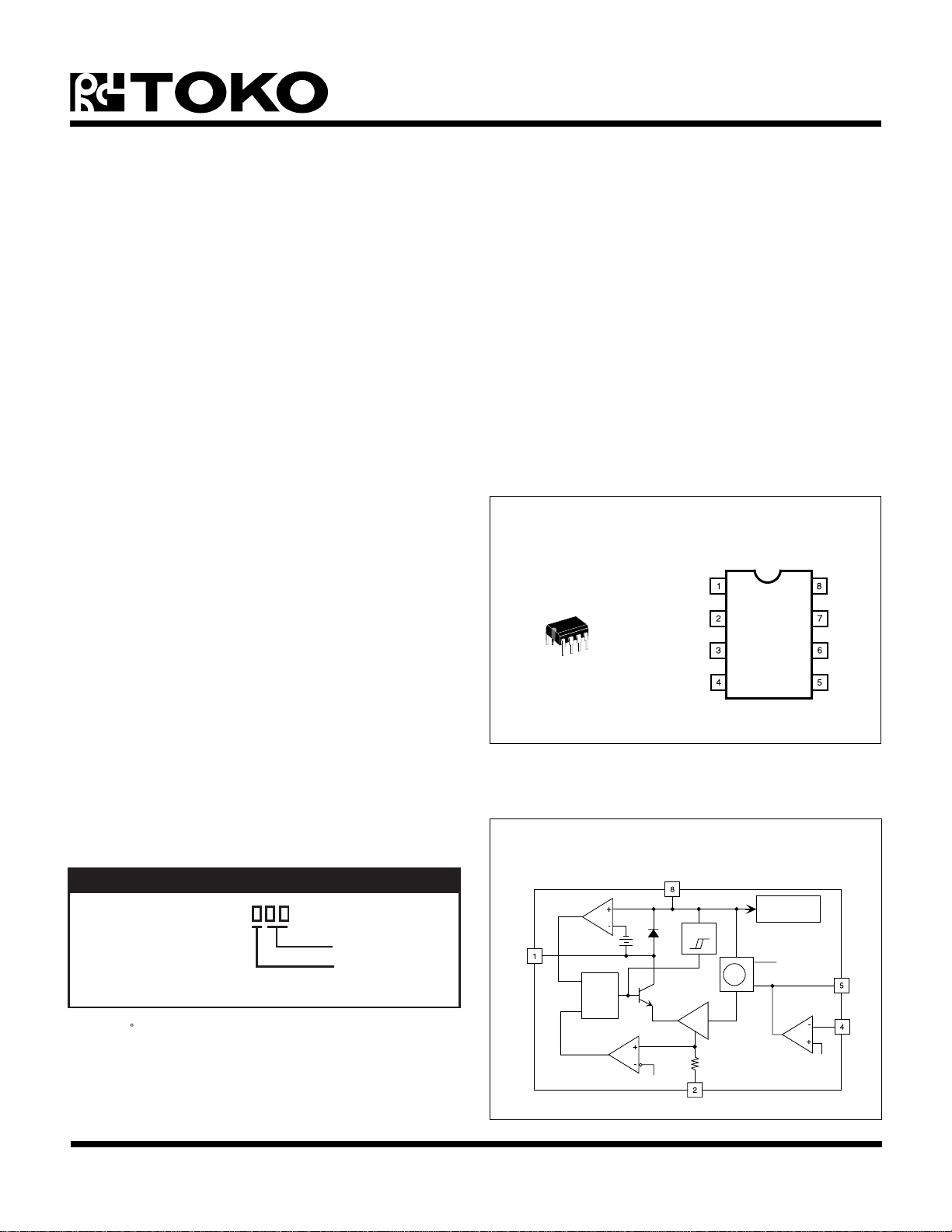
TK75002
75002
DRV
GND NC
NC
V
NC
COMPINV
CC
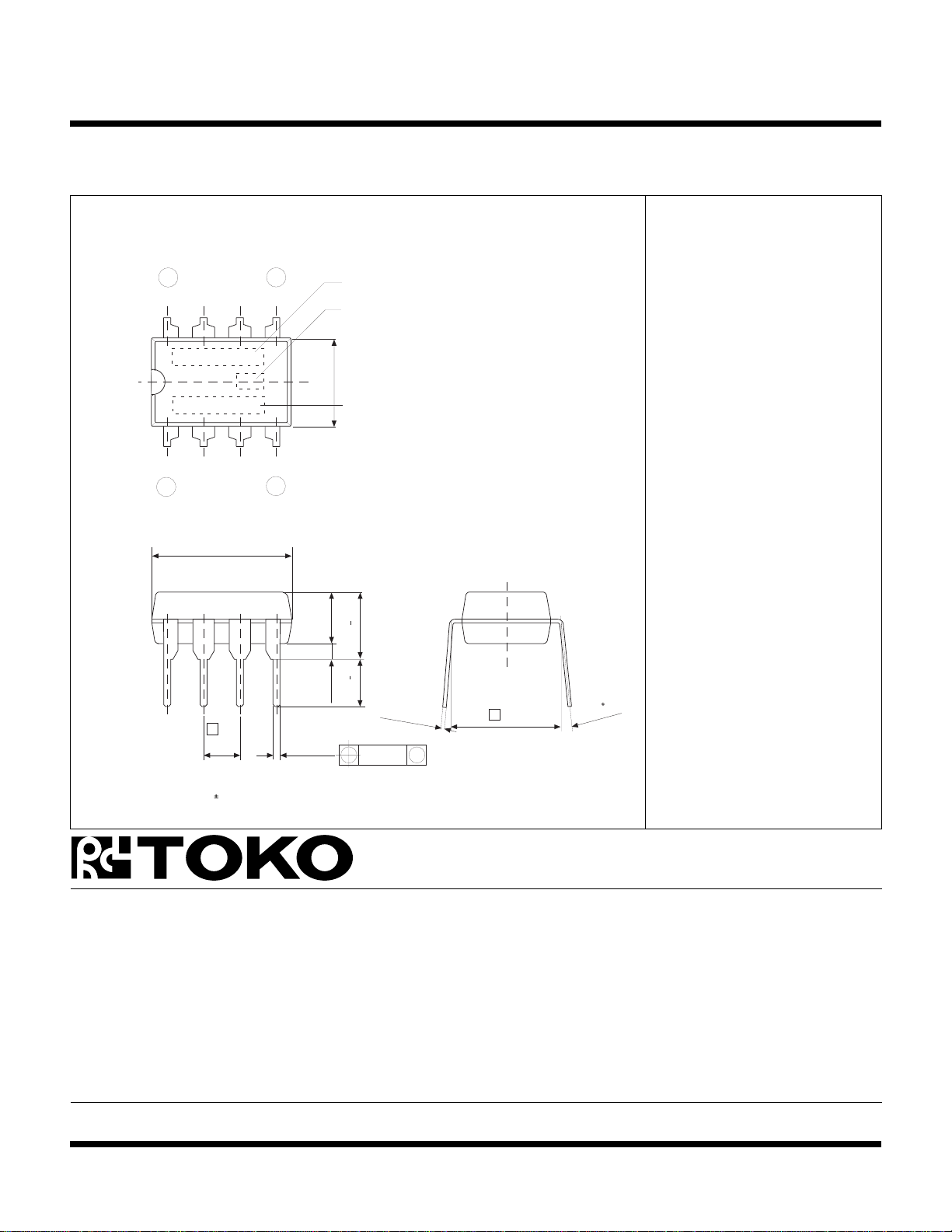
The TK75002 is available in an 8-pin DIP package.
BLOCK DIAGRAM
V
220 mV
CC
BUFFER
UVLO
GND
+
V
LS
-
ERROR AMPLIFIER
4 Ω
BANDGAP
REFERENCE
LEVEL SHIFTER
VLS = K(2.5 V - V
2.5 V
+
V
-
COMP
COMP
)
COMP
INV
1.35 V
ORDERING INFORMATION
TK75002D
EXTENDED TEMP. RANGE
I: -40 TO +85 C
Tape/Reel Code
Temperature Code
TAPE/REEL CODE
MG: Magazine
DRV
TRANSFORMER
RESET
DETECTOR
PAM LATCH
S
R
PEAK
CURRENT
DETECTOR
650 mV
Q
PAM SWITCH
January 1999 TOKO, Inc. Page 1
Page 2

TK75002
ABSOLUTE MAXIMUM RATINGS
Supply Voltage ........................................................... 7 V
Power Dissipation (Note 1) ................................ 825 mW
Storage Temperature Range ................... -55 to +150 °C
Operating Temperature Range ...................-20 to +70 °C
TK75002 ELECTRICAL CHARACTERISTICS
Test conditions: V
LOBMYSRETEMARAPSNOITIDNOCTSETNIMPYTXAMSTINU
= 5 V, T
CC
= Full Operating Range. Typical numbers apply at TA = 25 °C, unless otherwise specified.
A
Extended Temperature Range (I) .............. -40 to +85 °C
Operating Voltage Range............................... 1.6 to 12 V
Junction Temperature .......................................... 150 °C
Lead Soldering Temperature (10 s) ..................... 235 °C
I
)FFO(CC
I
)NO(CC
V
CC
V
)NO(CC
V
)TSYH(CC
siseretsyHOLVUV
tnerruCylppuSybdnatSV
CC
tnerruCylppuSgnitarepOnepOniPVRD5.951Am
egnaRegatloVgnitarepO7.47V
dlohserhThgiHOLVUV
V5.3=0010060001Aµ
V=
PMOC
PMOC
)AE(fer
V=
)AE(fer
5.31.47.4V
51021003Vm
)SNIPPMOCDNAVNI(NOITCESREIFILPMARORRE
T
V
)AE(fer
A
LO
egatloV
niaGpooLnepO3556Bd
ecnerefeRlanretnItnelaviuqE
A
T
A
C°52=033.1053.1073.1V
egnaRlluF=13.193.1V
WBGtcudorPhtdiwdnaB-niaG 5.4zHM
RSSPoitaRnoitcejeRylppuSrewoP0507Bd
I
I
I
)KNIS(PMOC
)CRS(PMOC
VNI
tnerruCsaiBV
tnerruCkniSmumixaMV
tnerruCecruoSmumixaMV
PMOC
PMOC
V=
VNI
VottrohS=
CC
246 Am
ottrohS=DNG52-81-5-Am
PMOC
2-2.02Aµ
)NIPVRD(NOITCESROTALUDOMEDUTILPMAESLUP
I
)KP(VRD
t
D,FFO
V-
V
CC
V
V
HT,DRT
)NO(VRD
V-
)FFO(VRD
CC
edoiD
remrofsnarT
dlohserhT
niPVRDotnoitceteD
dlohserhTtnerruCevirDkaeP035557Am
kaePmorfyaleDffo-nruT
esluPssorcAegatloVkaeP
pmalCssorcAegatloVkaeP
I
I
rotceteDteseRremrofsnarT
Hµ5=L05571053sn
I=
VRD
VRD
V,
≥ V58.25.38.4V
)KP(VRD
CC
Am05=6.08.02.1V
092056059Vm
kegatSretfihSleveLfoniaG00.152.154.1V/V
Note 1: Power dissipation is 825 mW when mounted as recommended. Derate at 6.6 mW/°C for operation above 25 °C.
Page 2 January 1999 TOKO, Inc.
Page 3
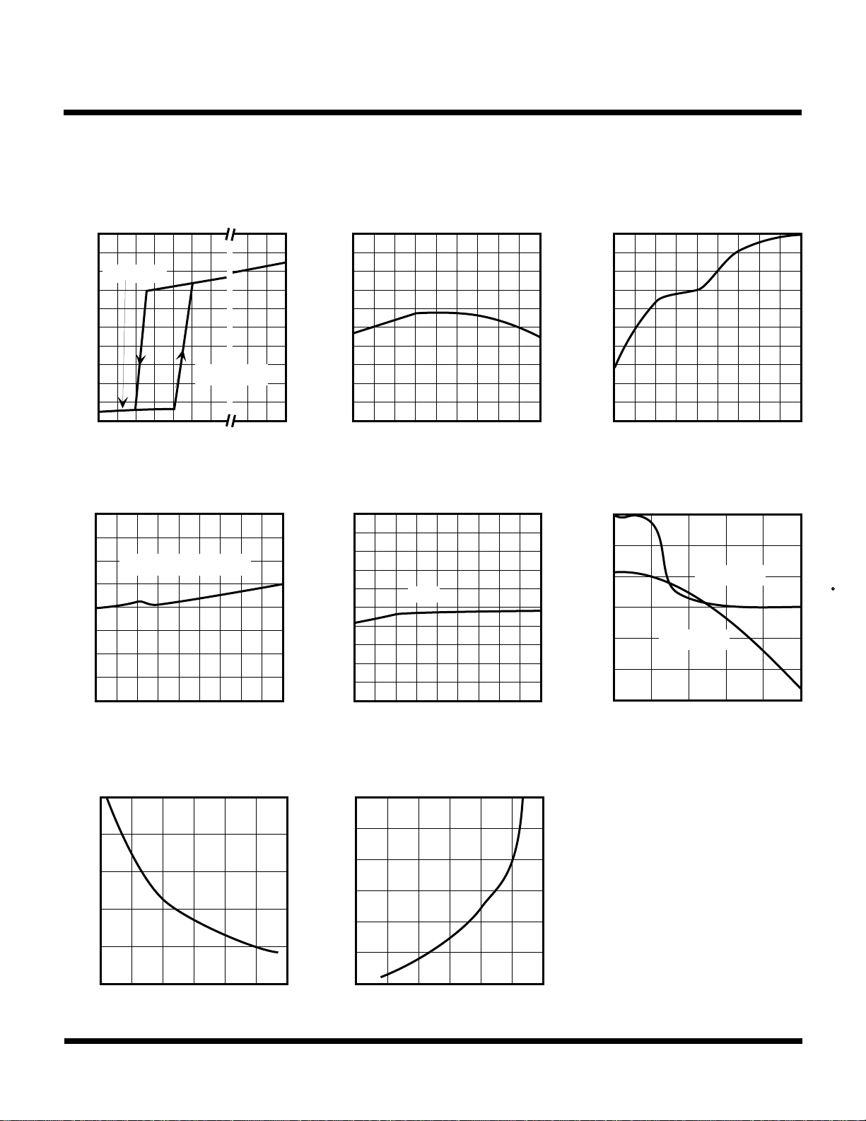
TYPICAL PERFORMANCE CHARACTERISTICS
GAIN (dB)
20
60
GAIN AND PHASE OF ERROR AMP
FREQUENCY (Hz)
0
10
2
103 104 105 106 10
7
40
-20
80
100
PHASE (°)
GAIN (dB)
180
150
120
90
60
30
0
PHASE ( )
TK75002
SUPPLY CURRENT vs.
SUPPLY VOLTAGE
12
10
STANDBY
8
(mA)
CC
I
6
4
0
3.8 4.0 4.1 4.2 5 7
PEAK DRIVE CURRENT THRESHOLD
80
70
(mA)
60
DRV(PK)
I
50
vs. TEMPERATURE
OVER SUPPLY RANGE
DEVICE ON
VCC (V)
INTERNAL REFERENCE VOLTAGE
vs. TEMPERATURE
1.40
1.38
1.36
(V)
ref
V
1.34
1.32
1.30
-40 0 40 80 120
TA (°C)
GAIN OF LEVEL SHIFTER (k) vs.
1.50
1.40
1.30
1.20
GAIN (V/V)
1.10
TEMPERATURE
5 V
PEAK VOLTAGE ACROSS
TRANSFORMER vs. TEMPERATURE
3.5
3.3
3.1
(V)
PK
V
2.9
2.7
2.5
-40 0 40 80 120
TA (°C)
40
-40 0 40 80 120
FREQUENCY vs. INDUCTOR
1.0
0.8
0.6
0.4
FREQUENCY (MHz)
0.2
0.0
0 10 20 30 40 50 60
INDUCTANCE (µH)
January 1999 TOKO, Inc. Page 3
TA (°C)
(V
CC
= 5 V)
(mA)
I
1.00
-40 0 40 80 120
TA (°C)
SUPPLY CURRENT vs. FREQUENCY
50
45
40
35
CC
30
25
20
0 0.2 0.4 0.6 0.8 1.0 1.2
(VCC = 5 V)
FREQUENCY (MHz)
Page 4
TK75002
THEORY OF OPERATION
The TK75002 can be used in conjunction with either an
opto-coupler or a pulse transformer to isolate an error
signal developed by its internal op-amp. The op-amp can
be externally compensated and features a precision
reference voltage at the non-inverting input. When
configured to drive a pulse transformer, the TK75002 will
automatically oscillate to drive the pulse transformer in a
pulse-amplitude-modulation (PAM) mode.
When VCC is below the UVLO threshold (~4.1V) the
TK75002 does not operate and the DRV pin remains in a
high-impedance state. When VCC is above the UVLO
threshold, the PAM switch turns on and forces V
DRV
with
respect to VCC to be equal to a gain constant times the opamp output voltage, V
, with respect to 2.5 V.
COMP
Essentially, then, the inverse of the error voltage (referenced
to 2.5 V, a virtual ground) times a small gain constant is
what appears between the DRV and VCC pins. Note that
this is only valid when V
implies that V
is less than VCC.
DRV
is less than 2.5 V, which also
COMP
If an opto-coupler and series resistor are hooked between
the DRV and VCC pins, an error current is transmitted
across the opto-coupler which is free from the characteristic
of having the zero that is a sort of parasitic effect of the
standard configuration of driving an opto-coupler with a
TL431.
The TK75002 has a saturation limiter in the feedback loop.
For either the opto-coupler or pulse transformer
configurations, the error voltage which is transmitted across
the isolation device by the TK75002 is limited to less than
5 V. This limiting occurs regardless of the applied V
CC
(generally, it is VCC which is being regulated by the feedback
loop for which the TK75002 transmits the error signal).
Thus, when the TK75002 is used in a variable output
voltage power supply or in a standard line of various fixed
output power supplies, no supplemental signal-limiting
circuitry is required in the feedback loop.
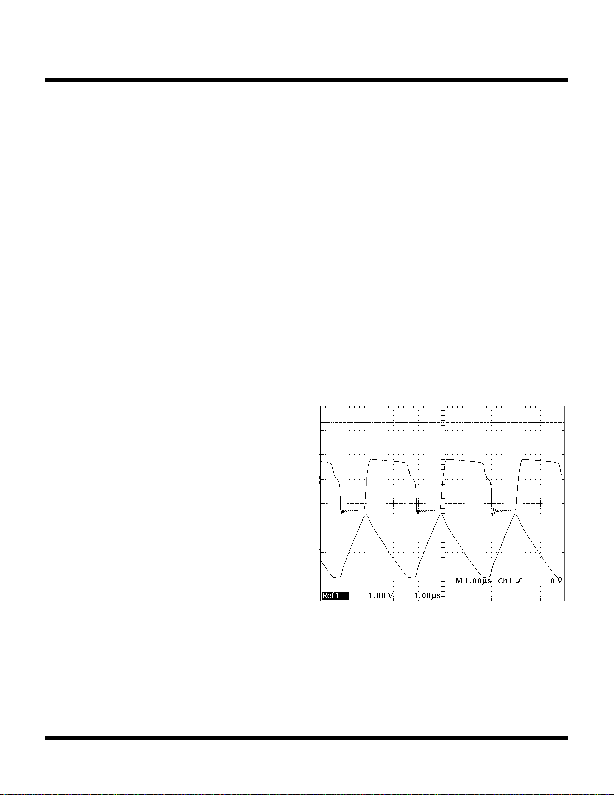
The characteristic waveforms of the TK75002 driving a
pulse transformer are shown in Figure 1. The top trace
shows the error voltage (@ 1 V / div.) referenced two
divisions below the top; it is equal to approximately 1.3 V.
The middle trace shows the DRV Pin voltage with respect
to VCC (@ 1 V / div.) referenced three divisions below the
top. The bottom trace shows the DRV Pin current (@ 20
mA / div.) referenced one division above the bottom.
If a pulse transformer is connected between the DRV and
VCC pins, the magnetizing current will begin to increase
until it reaches a threshold of ~ 55 mA, as detected by the
Peak Current Detector. After an internal turnoff delay, the
PAM switch turns off and the magnetizing current forces
the DRV-pin voltage above VCC. An internal clamp diode
between the DRV pin and the VCC pin clamps the voltage
and then essentially compares it to a VCC-referenced
voltage which corresponds to ~ 1 mA of current flow in the
clamp diode (i.e., ~ 650 mV at room temperature). When
the magnetizing current has decayed to nearly zero (i.e.,
~ 1 mA) and after an internal turn-on delay, the Transformer
Reset Detector turns on the PAM switch to initiate the
process all over again. By using peak rectification on the
secondary side of the pulse transformer, the error signal
FIGURE 1: CHARACTERISTIC WAVEFORMS OF THE
TK75002
can be recovered. The time constant of the peak detection
circuit is chosen to yield negligible ripple but also an
acceptable response time. The magnetizing inductance of
the pulse transformer is chosen to yield an acceptable
peak current overshoot and/or power dissipation when the
switching frequency is at a maximum (maximum switching
frequency occurs when the op-amp output is low).
Page 4 January 1999 TOKO, Inc.
Page 5

PIN DESCRIPTION
V
PIN
CC
This pin is connected to the supply voltage. The operation
of the IC is enabled when the supply voltage exceeds
4.1 V, which is the upper threshold of the undervoltage
lockout circuit. The operation is disabled when the supply
voltage drops below 3.98 V.
GND PIN
This pin provides ground return for the IC.
DRV PIN
This pin drives the first terminal of the primary winding of
the external pulse transformer using pulse-amplitude
modulation (PAM). The second terminal of the primary
winding is connected to the VCC pin. When the DRV pin is
low, an internal NPN transistor (the PAM switch) is turned
on and sinks an increasing current from the supply voltage
through the primary winding. The PAM switch is turned off
when the current reaches approximately 55 mA. The PAM
switch is turned on again when the transformer is reset
through the internal free-wheeling diode.
TK75002
INV PIN
The INV pin is the inverting input of the error amplifier. The
non-inverting input of the error amplifier is connected to an
internal 1.35 V precision reference source.
COMP PIN
The COMP pin is the output of the error amplifier. The
frequency compensation feedback network is connected
between the COMP and INV pins. Internally, the COMP pin
drives the inverting input of a level shifter stage. The roles
of the level shifter are to change (1) the reference point of
the error signal from the GND pin to the VCC pin (necessary
to avoid the parasitic zero in the transfer function caused
by feed-forward through the supply) and (2) the signal
polarity (necessary for start-up of the converter system in
case the reference point was changed). The parasitic zero
is discussed in the "Application Information" section.
January 1999 TOKO, Inc. Page 5
Page 6
TK75002
APPLICATION INFORMATION
THE PARASITIC ZERO AND HOW IT IS ELIMINATED IN
THE TK75002
In a feedback-regulated isolated power supply, isolation is
usually provided by an opto-coupler whose photodiode
section is connected between the output of the power
supply and the output of the error amplifier (in series with
a resistor that converts the voltage difference between the
two outputs into a current). Due to the feed-forward path
established by that connection, the transfer function of the
error amplifier is significantly modified (the modification in
the transfer function appears also if the opto-coupler is
replaced by the combination of a transformer and peak
detector driven by a pulse amplitude modulator).
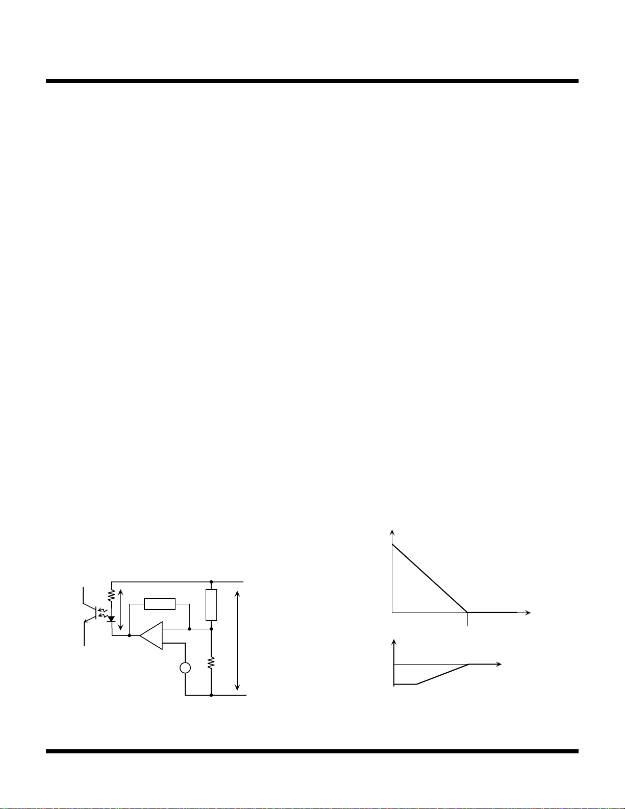
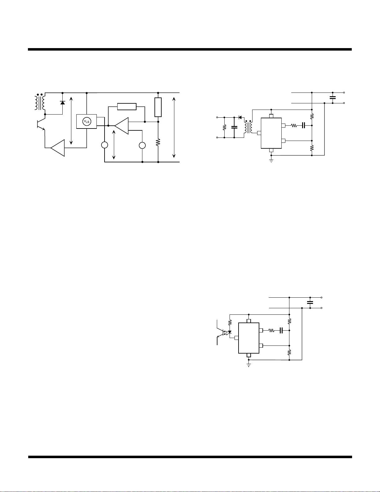
Figure 2 shows the error amplifier/opto-coupler
combination. The output voltage V2 (that is the voltage
measured across the photodiode and the series resistor)
can be written as:
V2 = V1 - [ - (ZFB / ZIN) x V1]
(1)
From (1), the transfer function of the error amplifier (from
the supply voltage V1, to the voltage V2) is:
H(s) = V2(s) / V1(s) = 1 + (ZFB / ZIN)
(2)
Figure 3 shows the magnitude and phase diagram of the
transfer function. As can be seen, the feed-forward path
adds a left half-plane zero (sometimes called a "parasitic"
zero) to the transfer function of the ideal integrator. The
parasitic zero is undesirable because it increases the high
frequency loop gain of the system, potentially leading to
subharmonic instability or chaotic behavior. To avoid the
effect of the zero, either a low pass (decoupling) filter must
be added to the supply rail of the opto-coupler, or an
additional pole must be introduced around the frequency
of the zero, or the loop gain must be reduced. (Note that
reducing the loop gain slows down the transient response
of the system.)
The TK75002 eliminates the parasitic zero by changing
the reference point of the error signal from the GND pin to
the VCC pin. That is achieved by inserting a level shifter
circuit between the output of the error amplifier and the
buffer of the pulse-amplitude modulator (see Figure 4).
The output voltage of the level shifter is proportional to the
error signal (i.e., the voltage of the COMP pin) and is
conveyed relative to the supply voltage V1. The end result
is that the transfer function becomes:
H(s) = ZFB / Z
IN
(4)
In the case when the feedback impedance is a capacitor C
and the input impedance is a resistor R, the transfer
function becomes:
H(s) = (1 + SRC) / SRC
In the case of a capacitive feedback impedance and
resistive input impedance, the transfer function will be that
of an ideal integrator, without the parasitic zero.
H (dB)
(3)
++
V
2
Z
FB Z
-
+
IN
V
1
+
R
B
V
ref
0
φ
0 °
-
-90 °
-20 dB / dec
1 / (2
f
πRC)
f
FIGURE 3: MAGNITUDE AND PHASE VS.
FIGURE 2: ERROR AMPLIFIER / OPTO-COUPLER
COMBINATION
FREQUENCY OF AN ERROR AMPLIFIER / OPTO-
COUPLER COMBINATION
Page 6 January 1999 TOKO, Inc.
Page 7
APPLICATION INFORMATION (CONT.)
TK75002
+
Z
FB
-
+
V
COMP
+
++
V
ref
V
2
-
2.5 V
+
Z
IN
V
1
R
B
-
FIGURE 4: ELIMINATING THE Feed-forward OF THE
SUPPLY VOLTAGE IN THE TK75002
ISOLATION WITH PULSE TRANSFORMER
Figure 5 shows an application where the error signal is
isolated with a pulse transformer. The signal is recovered
at the primary side with a peak detector. The circuit is selfoscillating. The frequency of operation is:
f = VF / [[(I
DRV(PK)
x LM) / kV
COMP
+ t
OFF(D)
] x (kV
COMP
+ VF)]
(5)
where the various quantities are:
V
I
DRV(PK)
L
M
forward voltage drop of the internal clamp diode
F
peak drive current threshold
magnetizing inductance of the pulse transformer
k gain of level shifter stage
t
OFF,D
V
turnoff delay from peak detection to DRV pin
error signal (voltage at the COMP pin)
COMP
A 20 µH magnetizing inductance, with the typical parameter
values of the TK75002 and an error signal of 1.4 V yields
about 500 kHz oscillation frequency. Such an inductance
can be obtained with three to five turns on a small ferrite
toroid core of 5 to 10 mm external diameter.
+
TO PRIMARY SIDE
CONTROLLER
OUTPUT OF ISOLATED
POWER SUPPLY
V
L
CC
M
n
n
2
1
COMP
DRV
INV
GND
FIGURE 5: ISOLATING THE ERROR SIGNAL WITH A
PULSE TRANSFORMER
ISOLATION WITH OPTO-COUPLER
Figure 6 shows how the TK75002 can be used together
with an opto-coupler. The oscillation is automatically
disabled because the peak current will never reach the
nominal 50 mA peak drive current threshold. A resistor
must be connected in series with the photodiode of the
opto-coupler to limit the maximum current. The main
advantage of the TK75002 over the TL431 is the left-halfplane zero is avoided. Another advantage is that the error
amplifier in the TK75002 has higher bandwidth than the
TL431.
OUTPUT OF ISOLATED
POWER SUPPLY
V
CC
COMP
DRV
INV
GND
+
FIGURE 6: ISOLATING THE ERROR SIGNAL WITH
AN OPTO-COUPLER
January 1999 TOKO, Inc. Page 7
Page 8

TK75002
APPLICATION INFORMATION (CONT.)
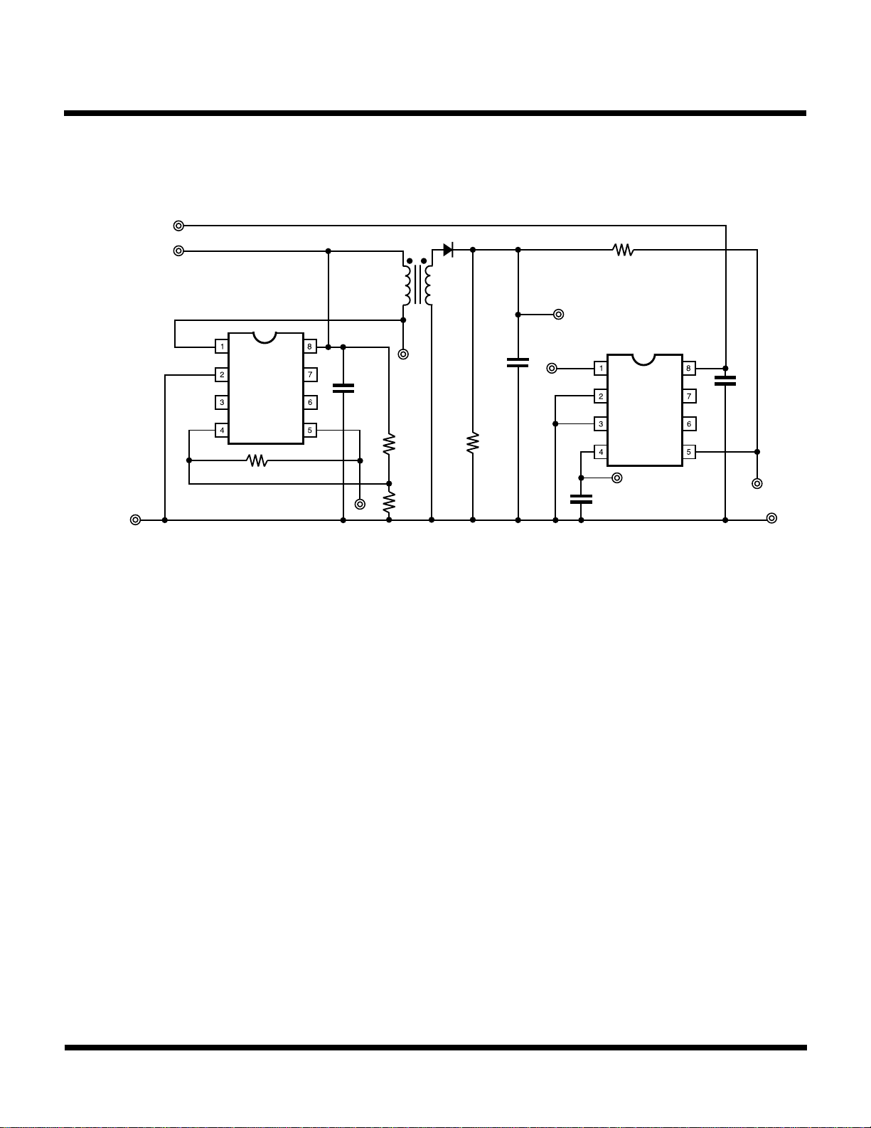
TEST CIRCUIT EXAMPLE
This simple circuit shown in Figure 7 is designed to allow
the user to probe and observe the characteristic
performance and behavior of either a TK75001 or a
TK75003 operating with a TK75002. Also, either IC can be
characterized independently in the circuit. The TK75001/
TK75003 are pulse width modulated (PWM) controllers.
The TK75002 is a pulse-amplitude-modulated (PAM)
controller.
In all of the following text, the TK75003 can be substituted
for the TK75001, depending on which of those two ICs is
used in the characterization circuit. Ground is common to
both the TK75001 and the TK75002.
V
provides power to the TK75001. V
CC1
up to around 15 V to turn on the TK75001. Turn-on can be
determined by any of the following events: a) current from
the V
supply jumps from ~ 1 mA to ~ 20 mA as the
CC1
supply voltage is raised, b) a timing waveform appears at
TP5, or c) a drive signal appears at TP6 (assuming that TP
or TP4 is held low). TP5 is the timing pin of the TK75001,
which has a sawtooth voltage waveform across the 1000
pF timing capacitor. TP4 is the feedback pin. The user can
force a voltage there directly (for example, to measure the
threshold voltage of the PWM, V
, which is approximately
CCD
0.92 V) or voltage can be applied at TP3. Applying the
voltage at TP3 allows a voltage ramp to form and the PWM
characteristic to be observed. The modulation range from
zero to maximum PWM is approximately 0 to 1 V of voltage
applied to TP3. The higher the applied voltage, the narrower
the pulse width. Finally, in order to see the TK75001
operating with the TK75002, the voltage at TP3 can be
applied by causing the TK75002 to operate, as described
next.
must be brought
CC1
3
V
provides power to the TK75002. The TK75002 is
CC2
configured with a resistor-feedback limited DC gain from
V
so that a gradual PAM change can be easily observed
CC2
as V
maximum PAM is approximately 5 to 6 V of applied V
is changed. The modulation range from zero to
CC2
CC2
.
The higher the VCC the higher the PAM signal magnitude.
The PAM signal can be observed by probing TP2, although
it is more easily understood when connecting the probe
ground to V
since PAM is with respect to the supply
CC2
voltage in the TK75002. The peak-rectified transformercoupled output of the TK75002 can be observed at TP3.
Page 8 January 1999 TOKO, Inc.
Page 9
TK75002
APPLICATION INFORMATION (CONT.)
V
CC1
V
CC2
TP
DRV
V
CC
3.3 k
3
GND2
GND
NC
INV
TK75002
33 k
NC
NC
COMP
0.1 µF
TP
TP
2
10 k
1
3.9 k
1 nF
3.3 k
FIGURE 7: TEST CIRCUIT SCHEMATIC
DRV
TP
6
GND
T
1000 pF
TK75001
OR
TK75003
TP
5
GND
C
V
CC
NC
0.1 µF
NC
FB
TP
4
GND
1
January 1999 TOKO, Inc. Page 9
Page 10
TK75002
PACKAGE OUTLINE
DIP-8
Marking Information
8
1
9.5
e
2.54
5
4
0.46
+ 0.15
- 0.05
Marking
Lot Number
6.4
Country of Origin
0.3
+
3.3
0.3
+
0.5 min
3.8
3.3
0.25
0.25
+ 0.15
- 0.05
e1
7.62
M
0 ~15
Marking
TK75002 75002
Dimensions are shown in millimeters
Tolerance: x.x = 0.2 mm (unless otherwise specified)
Toko America, Inc. Headquarters
1250 Feehanville Drive, Mount Prospect, Illinois 60056
Tel: (847) 297-0070 Fax: (847) 699-7864
TOKO AMERICA REGIONAL OFFICES
Midwest Regional Office
Toko America, Inc.
1250 Feehanville Drive
Mount Prospect, IL 60056
Tel: (847) 297-0070
Fax: (847) 699-7864
Western Regional Office
Toko America, Inc.
2480 North First Street , Suite 260
San Jose, CA 95131
Tel: (408) 432-8281
Fax: (408) 943-9790
Eastern Regional Office
Toko America, Inc.
107 Mill Plain Road
Danbury, CT 06811
Tel: (203) 748-6871
Fax: (203) 797-1223
Semiconductor Technical Support
Toko Design Center
4755 Forge Road
Colorado Springs, CO 80907
Tel: (719) 528-2200
Fax: (719) 528-2375
Visit our Internet site at http://www.tokoam.com
The information furnished by TOKO, Inc. is believed to be accurate and reliable. However, TOKO reserves the right to make changes or improvements in the design, specification or manufacture of its
products without further notice. TOKO does not assume any liability arising from the application or use of any product or circuit described herein, nor for any infringements of patents or other rights of
third parties which may result from the use of its products. No license is granted by implication or otherwise under any patent or patent rights of TOKO, Inc.
Page 10 January 1999 TOKO, Inc.
All Rights Reserved
IC-162-TK75002
0798O0.0K
Printed in the USA© 1999 Toko, Inc.
 Loading...