

Page 1
TK75020
ZVS RESONANT CONTROLLER
FEATURES
■ Optimized for Off-Line and Battery Powered
Operation
■ Internal Zero-Voltage Detector
■ Soft-Start
■ Pulse-by-Pulse Current Limit
■ Overdissipation Protection with Soft-Start
■ Overvoltage Protection with Soft-Start
■ Low-Current Standby mode
■ Programmable On/Off Timing
■ Enable Control
DESCRIPTION
The TK75020 is a low-cost, high-performance Zero-Voltage
Switching (ZVS) controller IC. The primary applications
are in inverters for Cold Cathode Fluorescent Lamps
(CCFL) and in ZVS quasi-resonant or multi-resonant
converters. The combination of a unique (patent-pending)
control concept and a ZVS resonant inverter generates
low-distortion sine wave for the fluorescent lamp, leading
to extended lamp life and high luminous efficiency. The IC
features all necessary circuits of a controller for such
applications, including externally adjustable timing
parameters (frequency, T
Soft-Start, enable, error amplifier, and a trimmed reference.
The same reference is used for undervoltage protection
and other critical internal biases. Supply current in the “off”
mode is kept at a minimum level (2 µA typical). Special
care has been taken to avoid undesirable turn-on of the
external power MOSFET when sufficient supply voltage is
not available, or when the device is held in the off mode.
Even with no Vcc applied, the drive pin of the IC will sink in
on(min)
, T
), current limit,
off(max)
APPLICATIONS
■ Cold Cathode Fluorescent Lamps
■ Resonant Power Supplies
■ Power Supplies for Notebook Computers
■ Power Supplies for Personal Electronics
excess of 20 mA while maintaining the voltage below 1 V
to prevent that leakage currents turn on the power MOSFET.
An internal zero-voltage detector monitors the voltage
across the MOSFET and ensures that the turn-on will only
take place under zero-voltage conditions. A unique
overdissipation protection prevents the overheating of the
power MOSFET in case the zero-voltage switching is lost.
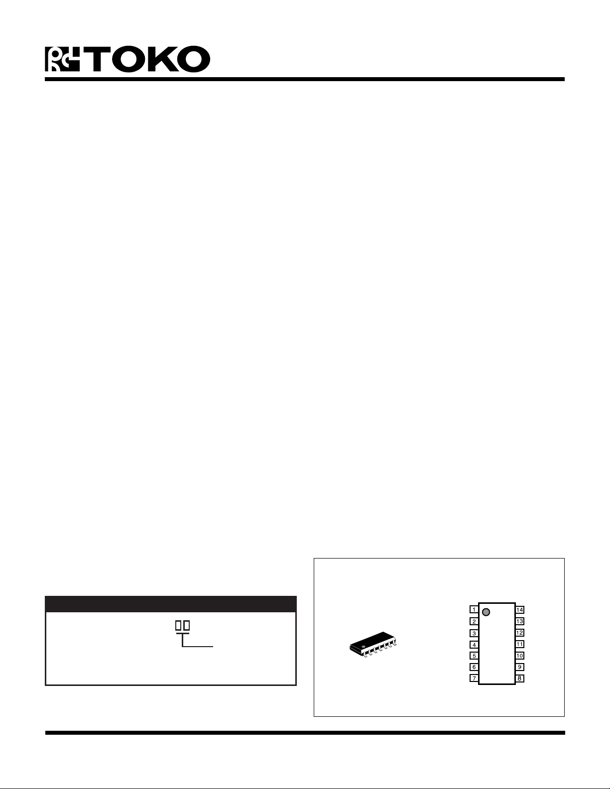
The TK75020 is available in a 14-lead surface mount
package.
TK75020
ORDERING INFORMATION
TK75020
Tape/Reel Code
TAPE/REEL CODE
TL: Tape Left
75020
T
OFF(MAX)
TON/SS
DRV
GND
OVP
EN
C
V
CC
V
ref
C
L
ZVD
T
EA
EA
ODP
OUT
INV
January 1999 TOKO, Inc. Page 1
Page 2

TK75020
ABSOLUTE MAXIMUM RATINGS
All Pins Except TON / SS, T
ODP and EN (Low Impedance Source) ................... 16 V
TON / SS, T
, ref, CT, ODP Pins.......................... 6 V
OFF(MAX)
EN Pin ...................................................................... 16 V
Power Dissipation (Note 1) ................................ 500 mW
TK75020 ELECTRICAL CHARACTERISTICS
Test conditions: V
Temperature Range, Typical numbers apply at TA = 25 °C, unless otherwise specified.
LOBMYSRETEMARAPSNOITIDNOCTSETNIMPYTXAMSTINU
= 12 V, VEN = 2.4 V, CT = 360 pF, I
CC
OFF(MAX)
, V
REF
, CT,
Maximum Current (VCC and ZVD Pins).................. 20 mA
Storage Temperature Range ................... -55 to +150 °C
Operating Temperature Range ...................-20 to +85 °C
Junction Temperature .......................................... 150 °C
Lead Soldering Temperature (10 s) ..................... 235 °C
TON / SS
= I
TOFF(MAX)
= 50 µA, DRV is Open, TA = Full Operating
I
)FFO(CC
I
I
I
I
)H,FFO(CC
)OLVU(CC
)NO(CC
)VRD,NO(CC
V
)NO(CC
V
)FFO(CC
V
)TSYH(CC
FFOtnerruCylppuSV
HGIH,FFOtnerruCylppuSV
edoMOLVU,tnerruCylppuSV
V
NOtnerruCylppuS
V
VRD,NOtnerruCylppuS
V0=2001Aµ
NE
NE
CC
CC
CC
V,V0=
CC
V5=0070001Aµ
V6=7.46Am
V<V6
CC
C,V6=
V<V6
CC
V61=2Am
V61<8Am
VRD
Fn1=6.58Am
V61<01Am
dlohserhThgiHOLVU2.56.50.6V
dlohserhTwoLOLVU0.53.56.5V
siseretsyHOLVU08005Vm
)NIPNE(NOITCESFFO/NO
V
NE
I
NE
V
fer
|∆V
|∆V
I
Note 1: Power Dissipation is 500 mW when mounted as recommended. Derate at 4 mW/°C for operation above 25°C.
Note 2: Guaranteed by design.
|noitalugeRdaoLI<Am1-
)DAOL(fer
|noitalugeReniLV<V6
)ENIL(fer
)CS(fer
egatloVdlohserhTV<V6
tnerruCtupnI
V(NOITCESECNEREFER
FER
tnerruCtiucriCtrohSV
V61<4.04.2V
CC
V
NE
V
NE
V4.2=4Aµ
)2etoN(,V0=001-An
)NIP
T
egatloVtuptuOecnerefeRI
Am0=
fer
CC
V0=21-Am
fer
A
T
A
Am0<0.4Vm
fer
V61<51Vm
C°52=8.30.42.4V
egnaRlluF=7.30.43.4V
Page 2 January 1999 TOKO, Inc.
Page 3

TK75020 ELECTRICAL CHARACTERISTICS (CONT.)
Test conditions: V
Temperature Range, Typical numbers apply at TA = 25 °C, unless otherwise specified.
LOBMYSRETEMARAPSNOITIDNOCTSETNIMPYTXAMSTINU
= 12 V, VEN = 2.4 V, CT = 360 pF, I
CC
)NIPVRD(NOITCESEVIRD
TON / SS
= I
TOFF(MAX)
= 50 µA, DRV is Open, TA = Full Operating
TK75020
V
V
I
I
t
ESIR
t
LLAF
V
)fer(AE
I
)VNI(AE
V
A
LO
WBGtcudorPhtdiwdnaB-niaG
I
)HGIH(VRD
)WOL(VRD
)KP,CRS(VRD
)KP,KNIS(VRD
egatloVhgiHtuptuO
egatloVwoLtuptuO
tnerruCecruoSkaePC
tnerruCkniSkaePC
emiTesiRC
emiTllaFC
AE(NOITCESREIFILPMARORRE
VNI
VRD
I
VRD
I
VRD
I
VRD
I
VRD
V
NE
VRD
VRD
VRD
VRD
AEDNA
TUO
ecnerefeRlanretnItnelaviuqE
egatloV
Am02-=0.90.01V
Am001-=8.9V
Am02=3.06.0V
Am002=8.15.2V
V,Am02=
CC
V0=
roV0=
9.03.1V
Fn01=005Am
Fn01=007Am
Fn1=07021sn
Fn1=5257sn
)SNIP
91.162.103.1V
tnerruCsaiB 01.0Aµ
)WOL,TUO(AE
WOLegatloVtuptuOI
)TUO(AE
niaGpooLnepOk51 Ω AEmorF
k51 Ω AEmorF
)2etoN(
V,Am1-=
VNI
TUO
TUO
V5.1=52.0V
Tot
Tot
SS/07Bd
NO
,SS/
NO
2zHM
RSSPoitaRnoitcejeRylppuSrewoPV6 ≤ VCC≤ V6156Bd
C(NOITCESTIMILTNERRUC
I
LC
V
)HT(LC
t
)VRD(LC
I
V
V
V
)CS(SS/NOT
SS/NOT
)HT(SS
)HT(HCD
tnerruCsaiBV
VRDotyaleDV
egatloVniPI
)NIP
L
V0=2.0-Aµ
LC
egatloVdlohserhT 081012042Vm
LC
T(NOITCESTRATS-TFOSDNAGNITTESEMIT-NO
NO
tnerruCtiucriCtrohSV
SS/NOT
SS/NOT
)NIPSS/
V0=5.2-Am
Am0=8.10.22.2V
Vm004ot0morFspetS051sn
dlohserhTtratS-tfoS 04.056.009.0V
dlohserhTegrahcsiDPDO 0.14.19.1V
January 1999 TOKO, Inc. Page 3
Page 4

TK75020
TK75020 ELECTRICAL CHARACTERISTICS (CONT.)
Test conditions: V
Temperature Range, Typical numbers apply at TA = 25 °C, unless otherwise specified.
LOBMYSRETEMARAPSNOITIDNOCTSETNIMPYTXAMSTINU
= 12 V, VEN = 2.4 V, CT = 360 pF, I
CC
TON / SS
= I
TOFF(MAX)
= 50 µA, DRV is Open, TA = Full Operating
T(NOITCESGNITTESEMIT-FFOMUMIXAM
I
V
V
V
)XAM,FFO(T
)XAM,FFO(T
)WOL(TC
)HGIH(TC
egatloVniPI
C(NOITCESGNIMIT
)NIP
T
tnerruCtiucriCtrohSV
egatloVdlohserhTwoL9.00.11.1V
egatloVdlohserhThgiH7.20.33.3V
)NIP
)XAM(FFO
V0=5.2Am
)XAM,FFO(T
)XAM,FFO(T
Am0=8.10.22.2V
fycneuqerFrotallicsO511041561zHk
CotoitaRrefsnarTtnerruC
,niP
RTC
NOT
RTC
)XAM(FFOT
gnitteSemit-nO
gnitteSemit-ffOxaM
T
CotoitaRrefsnarTtnerruC
T
V
,niP
V
V4=2.6-5.5-8.4-
TC
V0=57.452.557.5
TC
)NIPDVZ(NOITCESROTCETEDEGATLOVOREZ
V
)HT(DVZ
I
DVZ
t
)VRD(DVZ
tnerruCtupnIV
VRDotyaleD
dlohserhTwoLrotceteDT
A
V
DVZ
C
VRD
C°52=8.10.22.2V
V2=05-0Aµ
DVZ
,V0ot5morFspetS
Fn1=
071003sn
)NIPPDO(NOITCESROTCETEDNOITAPISSIDREVO
V
)HT(PDO
I
)GVA(PDO
tnerruCegarevAT,zHk001=f
egaloVdlohserhTnoitceteD54.007.059.0V
PALREVO
sn002=6.0Aµ
)NIPPVO(NOITCESROTCETEDEGATLOVREVO
V
)HT(PVO
t
)D(PVO
VRDotylaeD 053008sn
egaloVdlohserhTnoitceteD6.30.43.4V
Page 4 January 1999 TOKO, Inc.
Page 5
T
OFF(MAX)
TON/SS
EA
TK75020
BLOCK DIAGRAM
V
CC
ZVS DRIVE
REF
- V
B
Q
16
1.5 V
CMP
CMP
3 V
1 V
CMP
HIGH: RAMP DOWN
RQSG
4
4
3
S
R
2
G
1
G
2
S
DRV
Q
LATCH
Q
R
G
3
RQS
CL LATCH
EN
G
TIMER
+2 V
Q
9
R
1
1 K
C
T
R
2
1 K
OUT
EA
INV
Q
1.25 V
12
V
BE
Q
1A
1
Q
Q
3
4
Q
5
Q
A
2
2
ERROR AMP
Q
13
SOFT START CMP
2 V
BE
Q
11
Q
10
REF
Q
6
Q
7
ODP DISCHARGE CMP
Q
8
Q
V
REF
14
ODP LATCH
50 µA
ZVD CMP
2.5/2.7 V
B
1
V
CC
DRIVE
3
EN
3
STAND-BY GATE DISCHARGE
CURRENT LIMITER
CL CMP
0.21 V
REF
EN
4
5
ODP CUR SRC
Q
15
Q
17
D
1
ZVD
DRV
C
L
ODP
OVP
REF
V
V
GND
CC
REF
EN
V
CC
EN0
B0
START-UP BIAS
V
CC
EN OUT
BANDGAP REF
+4 V
5.8/5.3 V
UVLO CMP
REF BUFFER
REF CMP
OVERDISSIPATION VOLTAGE PROTECTION
V
CC
EN
1
B
1
EN
2
EN
1
B
2
BUFFERED BIAS
REF
3.0 V
2.0 V
1.5 V
1.25 V
1.0 V
0.21 V
HIGH: DRV ENABLED
BIAS
January 1999 TOKO, Inc. Page 5
Page 6

TK75020
PIN DESCRIPTION
SUPPLY VOLTAGE PIN (VCC)
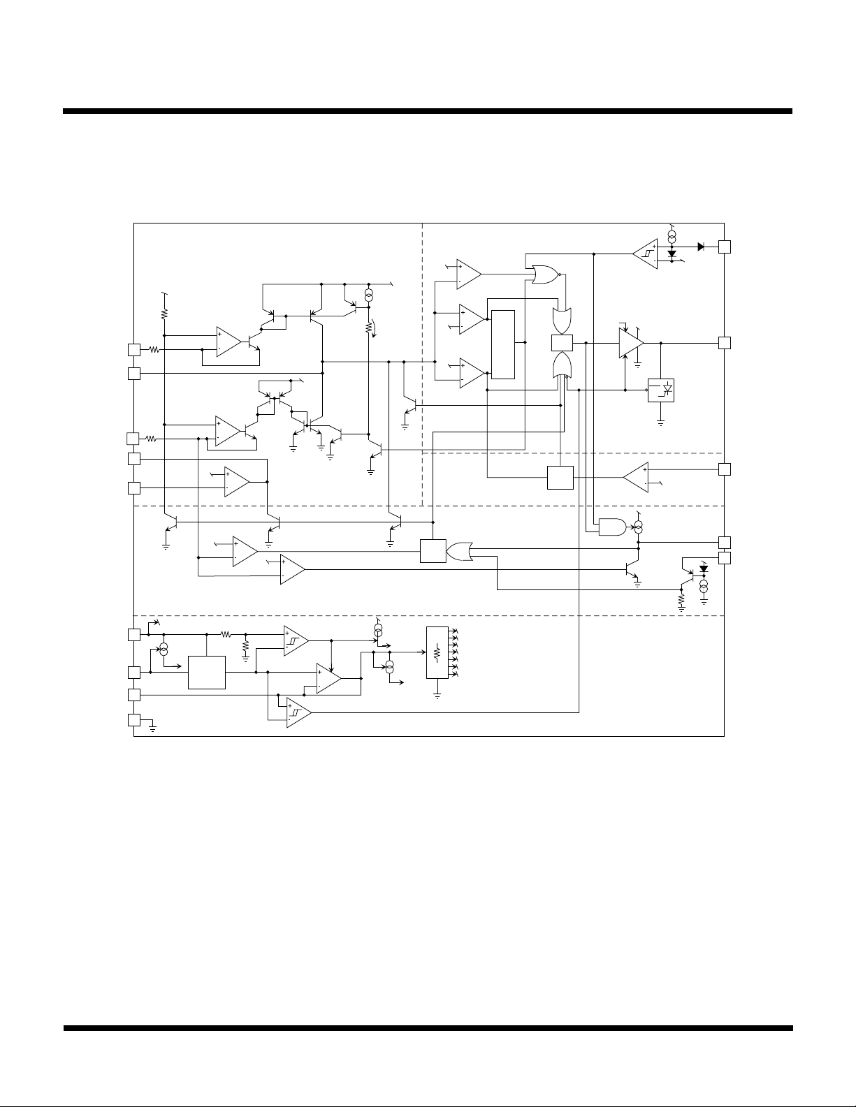
This pin is connected to the supply voltage. The IC begins
normal operation when two conditions are met: 1) the V
CC
voltage exceeds 5.6 V and 2) the voltage of the enable pin
exceeds 2.2 V. Operation ceases and the IC goes into a
UVLO mode when the VCC voltage drops below 5.3 V.
When the voltage at the enable pin becomes less than
0.4 V, the IC is turned off (“off” mode). In UVLO mode the
current consumption is less than 300 µA, in off mode it is
further reduced to below 3 µA. The operating voltage
range is 6 V to 14 V. The tolerances of the start and stop
voltages are 5.6 ± 0.4 V and 5.3 ± 0.3 V, respectively.
During normal operation the total IC current consumption
is less than 8 mA (no load, 100 kHz operation).
When VCC is applied to the device with the enable pin
pulled above 2.2 V (“on” mode), the following events will
occur:
First, a trimmed bandgap reference voltage will be
generated as soon as VCC reaches about 4.8 V. This
reference will be used to determine the UVLO thresholds.
When VCC reaches the upper threshold of the undervoltage
lockout comparator, that comparator enables the reference
buffer. When the voltage at the output of the buffer, i.e. on
the V
pin, becomes higher than about 3.7 V, an enable
REF
signal is generated for the drive stage through gate G3.
Normal operation may be interrupted at any time by pulling
the enable pin below 0.4 V. When VCC is reduced below the
lower threshold of the undervoltage lockout, the internal 4
V bias is disabled and the drive output is quickly turned off.
The bandgap reference remains active as long as V
CC
above 4.8 V. Special care has been taken to keep the drive
output low even at a lower level of VCC in order to prevent
unwanted turn-on of the external MOSFET.
ENABLE (ON/OFF) PIN (EN)
The enable pin is used to enable or disable the IC. The IC
is guaranteed to turn on (i.e., to enter the “on” mode) when
the pin voltage is above 2.2 V and is guaranteed to turn off
when the pin voltage is below 0.4 V. If the On/Off feature
is not needed, the pin can be connected directly to the
supply voltage. The enable pin is internally equivalent to a
200 kΩ resistor in series with two diodes.
GROUND PIN (GND)
This pin provides ground return connection for the IC.
DRIVE PIN (DRV)
This pin drives the external MOSFET. During standby, the
DRV pin provides at least 20 mA current sinking capability
with less than 1 V difference between the ground and the
DRV pin. The internal circuitry connected to the DRV pin
is designed to deliver a peak output voltage of 4 V above
ground when the device operates at a minimum supply
voltage of 6 V. An internal clamp circuit, however, ensures
that the peak output voltage will never exceed 13 V. The
DRV pin goes high only if the following five conditions are
met simultaneously: 1) the drive (DRV) latch is set, 2) the
overdissipation protection latch (ODP) is reset, 3) the
current limit latch (CL) is reset, 4) the enable pin is pulled
high, and 5) the output of the reference comparator is high,
i.e., it detects that the voltage at the V
pin is sufficiently
ref
high.
CURRENT LIMIT PIN (CL)
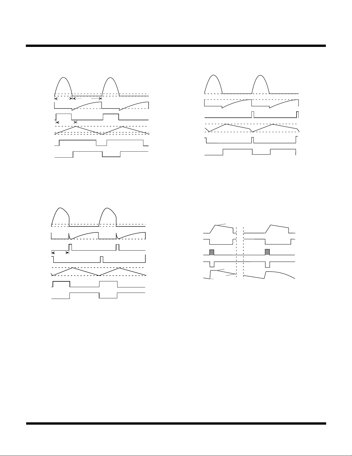
The CL pin is used for high-speed, cycle-by-cycle overload
protection. When the voltage of the CL pin exceeds 0.2 V
above ground, the current limit latch is set by the C
comparator and the output stage is forced low. At the same
time, the timing capacitor is quickly discharged with
transistor Q16. Note that a quick discharge is necessary in
order to reduce the “on” time (and the duty ratio) without a
significant increase in the effective “off” time. The current
limit latch is reset when the output of the drive latch goes
low, i.e., when the off time is over and the output of the C
comparator goes high.
is
REFERENCE PIN (V
ref
)
The bandgap reference, an internal 4 V source, is buffered
by a reference buffer, whose output is connected to the V
pin. The V
pin voltage is enabled to develop when the
ref
upper threshold of the UVLO comparator is passed by VCC.
TIMING CAPACITOR PIN (CT)
The external timing capacitor is connected to the CT pin.
The voltage across the timing capacitor oscillates between
an upper level of 3 V and a lower level of 1 V. During the
time the voltage of the timing capacitor is rising (due to the
charging current set by the resistor between ground and
the T
OFF( MAX)
pin), the drive latch is in the reset state and
L
L
ref
Page 6 January 1999 TOKO, Inc.
Page 7

PIN DESCRIPTION (CONT.)
TK75020
the DRV pin is held low. The drive latch may be set either
by the output of comparator CMP3 through the two-input
OR gate G2 or by the ZVD comparator through G1 and G2.
CMP3 detects if the timing voltage reached 3 V, the ZVD
comparator detects if the voltage at the ZVD pin dropped
below 2 V. Note that gate G1 allows setting the drive latch
through the ZVD pin only when the voltage at the CT pin is
higher than 1.5 V and the current limit latch is in the reset
state. The reason for disabling the ZVD path at CT pin
voltages lower than 1.5 V is to prevent an immediate turnon of the MOSFET after it was turned off. CMP4 is used to
detect if the CT pin voltage is higher than 1.5 V.
When the voltage of the timing capacitor is falling (due to
the discharging current set by the external resistors between
the output of the error amplifier and the TON/SS pin, as well
as between the TON/SS pin and ground), the DRV pin is
allowed to go high. The charge and discharge currents are
enabled exclusively.
ZERO VOLTAGE DETECTION PIN (ZVD)
This pin is connected to the drain of the power MOSFET
switch of the converter or inverter through a high value
resistor or a diode. When the MOSFET is turned off, the
drain voltage increases at first and then decreases, due to
the resonant action in the loading network of the switch.
When the drain voltage is above the supply voltage of the
IC, the ZVD pin voltage is clamped to the supply voltage
through the internal diode D1. As the drain voltage drops
below the supply voltage, the voltage of the ZVD pin begins
to follow it. When the ZVD pin voltage drops below 2 V, the
output of the ZVD comparator goes high and sets the drive
latch through gates G1 and G2. Unless there is a fault
condition, the DRV pin goes high and turns on the MOSFET
switch. By having the ZVD feature, the circuit automatically
sets the optimum off time, essentially independently from
the value of the resistor between the T
OFF(MAX)
pin and
ground.
ERROR AMPLIFIER PIN (EA
The EA
pin is the output of the internal error amplifier.
OUT
OUT
)
The output stage of the amplifier is an open-collector
transistor. It is normally connected to the TON/SS pin via an
external resistor. The non-inverting input of the error
amplifier is internally tied to a trimmed 1.25 V reference.
The error amplifier is short-circuit protected.
ERROR AMPLIFIER INPUT PIN (EA
The EA
pin (the inverting input of the error amplifier)
INV
INV
)
serves for receiving either an external voltage-feedback or
an external current-feedback signal. The compensating
network of the feedback loop is usually connected between
the EA
and the EA
INV
OUT
pins.
TURN-ON TIMING / SOFT-START PIN (TON / SS)
The on-time is inversely proportional to the current flowing
in the resistor connected between this pin and the EA
OUT
pin. The TON/SS pin is also useful for providing Soft-Start
at turn-on. Soft-Start can be achieved by connecting the
series combination of a resistor and capacitor between the
TON/SS pin and ground. When the normal operation of the
IC is enabled (either because the VCC voltage exceeds the
upper UVLO threshold or because the IC is turned on by
the Enable pin), the Soft-Start capacitor, which was initially
discharged, begins to charge up through the series resistor.
The charging current adds to the current flowing in the ontime-setting resistor and sets a shorter on time. As the
voltage builds up across the soft-start capacitor the charging
current gradually decreases and the on time gradually
increases.
At normal operation a voltage-to-current converter formed
by A2 and Q2 keeps the voltage of the TON/SS pin at 2 V.
The current flowing through R2 and the external resistor
connected to the TON/SS pin and ground is mirrored with
Q3 and Q4 into a second mirror formed by Q5 and Q6. The
diode-connected section of the second mirror is shorted
with the transistor Q7 via Q8 when the current switch latch
is reset.
MAXIMUM TURNOFF TIMING PIN (T
OFF(MAX)
)
An external resistor connected between this pin and ground
sets the current that charges the timing capacitor. The
maximum possible off time is inversely proportional to the
value of that current. As discussed previously, when the off
period is terminated by the zero-voltage detector, the
actual off time becomes shorter than the value set by this
resistor.
At normal operation the voltage of the T
OFF (MAX)
pin is kept
at 2 V with the help of a voltage-to-current converter
formed by the amplifier A1 and transistor Q1. The current
flowing through the off time setting resistor and R1 is
January 1999 TOKO, Inc. Page 7
Page 8

TK75020
PIN DESCRIPTION (CONT.)
mirrored by the transistors Q9 and Q10 and it charges the
timing capacitor. The incoming mirror current is diverted
from the mirror with transistor Q11 when the drive latch is
set.
OVERDISSIPATION PROTECTION PIN (ODP)
The ODP pin is used to realize a protection against
overdissipation of the power MOSFET due to the loss or
absence of zero-voltage switching (ZVS). (ZVS can be lost
if the load or the input voltage changes too much. ZVS is
absent if the component values of the load network are far
from optimal, or if the ZVD function is not implemented and
the set off time is either too short or too long.) If ZVS is not
present in a converter or inverter that was originally meant
to operate with it, the MOSFET is turned on with a substantial
voltage across it and the capacitor in parallel with it. Due
to the periodic discharge of the parallel capacitor, a
significant dissipation appears in the MOSFET. That
dissipation is proportional to the switching frequency, the
capacitance value, and the square of the voltage across
the MOSFET at the instant of turn-on. The overdissipation
protection works as follows: a current source is enabled
when the MOSFET drain voltage is above the ZVD
comparator threshold when the DRV pin voltage goes
high. A short current pulse flows into the parallel combination
of a resistor and capacitor connected between the ODP
pin and ground and gradually begins to raise the pin
voltage. When the pin voltage reaches about 0.7 V, the
ODP latch is set via gate G4. The output signal of the ODP
latch inhibits gate G3 and forces the drive output low. The
output of the ODP latch also turns on transistors Q12-Q14.
Q12 removes the 2 V reference signal from the noninverting input of amplifiers A1 and A2 . Q13 pulls down the
EA
pin. The Soft-Start capacitor connected to the TON/
OUT
SS pin begins to discharge through the soft-start resistor
(see application circuit) and the on-time setting resistor.
When the voltage at the TON/SS pin drops below 2 VBE, the
ODP discharge comparator turns on Q15, which pulls down
the ODP pin voltage and discharges the capacitor
connected to that pin. When the voltage at the TON/SS pin
drops below a VBE, voltage the Soft-Start comparator
resets the ODP latch. At that time the 2 V reference is
enabled and a new Soft-Start cycle begins. The turnoff/soft
restart cycle repeats until zero-voltage switching is
reestablished.
winding of the transformer in the CCFL inverter. When the
OVP comparator detects an overvoltage, it initiates a
shutdown via G4 and a Soft-Start cycle begins.
OVERVOLTAGE PROTECTION PIN (OVP)
The OVP pin is used to monitor the voltage across a
Page 8 January 1999 TOKO, Inc.
Page 9
V
SW
i
SW
ZVD
CMP
CMP4
DRV LATCH
Q
TK75020
APPLICATION INFORMATION
V
2.0 V
T
OFF
T
OFF(MAX)
C
T
T
ON
0
0
3.0 V
1.5 V
1.0 V
SW
i
SW
CL CLAMP
CL LATCH
Q
DRV LATCH
Q
0
0.2 V / R
SENSE
C
T
3.0 V
1.0 V
V
SW
i
SW
CMP3
CMP2
C
ZVD
CMP
DRV LATCH
Q
NORMAL OPERATION
T
OFF(MAX)
T
OPERATION WITHOUT ZVD
2.0 V
3.0 V
1.0 V
CYCLE-BY-CYCLE CURRENT LIMIT
V
0
0
TON / S.S
ODP
CMP7
DRV
ODP
LATCH
0
BE
2.0 V
1.5 V
V
BE
OVERDISSIPATION PROTECTION
January 1999 TOKO, Inc. Page 9
Page 10
TK75020
V
J
1
6 TO 16 V
1
2
3
APPLICATION INFORMATION (CONT.)
IN
C
1
100 n
R
5
18 k
R
2
1 k
R
68 k
1
C
2
10 µF
Q
2
(Note 1)
R
22 k
C
680 p
F
1A
ODP
INV
EA
OUT
TON/SS
T
OFF
3
C
T
3
EN OVP
1
C
V
GND
ZVD
DRV
V
4
22 µ
16 V
CC
D
1
1N4148
Q
1
2SK1475
R
C
L
ref
47 k
6
C
100 n
5
L
270 µ
8RHB
1
L
82 µ
8RHB
C
10
10 n
C
6
47 n
T1 (Note 2)
2
n1= 19
470 k
R
100 k
n2= 1520
R
9
R
11
68 k
10
R
10 k
R
3.3 k
J
2
11
22
R
14
1 k
D
2
1N4148
13
C
9
100 n
12
CCFL
220-250 mm
Gen. Note: Q2 is not required if Q1 is an avalanche rated FET
Gen. Note: Part #CTX01-13154 (Call Toko Technical Support (719) 528-2200).
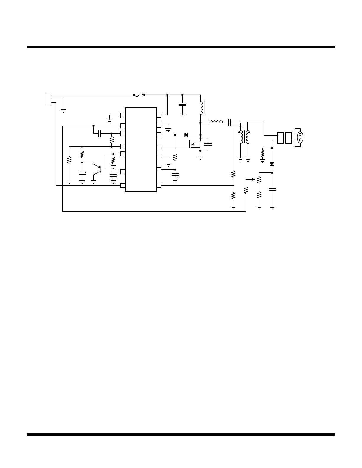
LAPTOP DISPLAY BACKLIGHTING EXAMPLE
Page 10 January 1999 TOKO, Inc.
Page 11
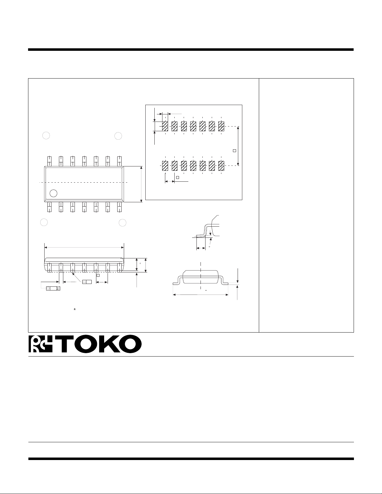
PACKAGE OUTLINE
TK75020
SOP-14
14
1
0.42
0.12
Marking Information
0.76
8
7
8.65
e
1.27
0.1
l
0.25 max
1.45
1.27
e
1.27
3.9
Recommended Mount Pad
0.5
6.07
0 ~10
+
0.3
0.3
+
1.64
5.4
1
e
0.2
Marking
TK75020 75020
Dimensions are shown in millimeters
Tolerance: x.x = 0.2 mm (unless otherwise specified)
Toko America, Inc. Headquarters
1250 Feehanville Drive, Mount Prospect, Illinois 60056
Tel: (847) 297-0070 Fax: (847) 699-7864
TOKO AMERICA REGIONAL OFFICES
Midwest Regional Office
Toko America, Inc.
1250 Feehanville Drive
Mount Prospect, IL 60056
Tel: (847) 297-0070
Fax: (847) 699-7864
Western Regional Office
Toko America, Inc.
2480 North First Street , Suite 260
San Jose, CA 95131
Tel: (408) 432-8281
Fax: (408) 943-9790
Eastern Regional Office
Toko America, Inc.
107 Mill Plain Road
Danbury, CT 06811
Tel: (203) 748-6871
Fax: (203) 797-1223
Semiconductor Technical Support
Toko Design Center
4755 Forge Road
Colorado Springs, CO 80907
Tel: (719) 528-2200
Fax: (719) 528-2375
Visit our Internet site at http://www.tokoam.com
The information furnished by TOKO, Inc. is believed to be accurate and reliable. However, TOKO reserves the right to make changes or improvements in the design, specification or manufacture of its
products without further notice. TOKO does not assume any liability arising from the application or use of any product or circuit described herein, nor for any infringements of patents or other rights of
third parties which may result from the use of its products. No license is granted by implication or otherwise under any patent or patent rights of TOKO, Inc.
January 1999 TOKO, Inc. Page 11
All Rights Reserved
IC-122-TK75020
0798O0.0K
Printed in the USA© 1999 Toko, Inc.
 Loading...