

Page 1
FEATURES
■ 20 ns Rise and Fall Times into 1000 pF
■ 550 µA Standby Current Consumption
■ Undervoltage Lockout Combined with First Pulse
Wake-Up Feature *
■ Cycle-by-Cycle Current Limiting
■ Current Sense Voltage Spike Cancellation when
Used with Gate Charge Recovery Circuit *
■ Thermal Overload Protection
■ TTL/CMOS Compatible Input
DESCRIPTION
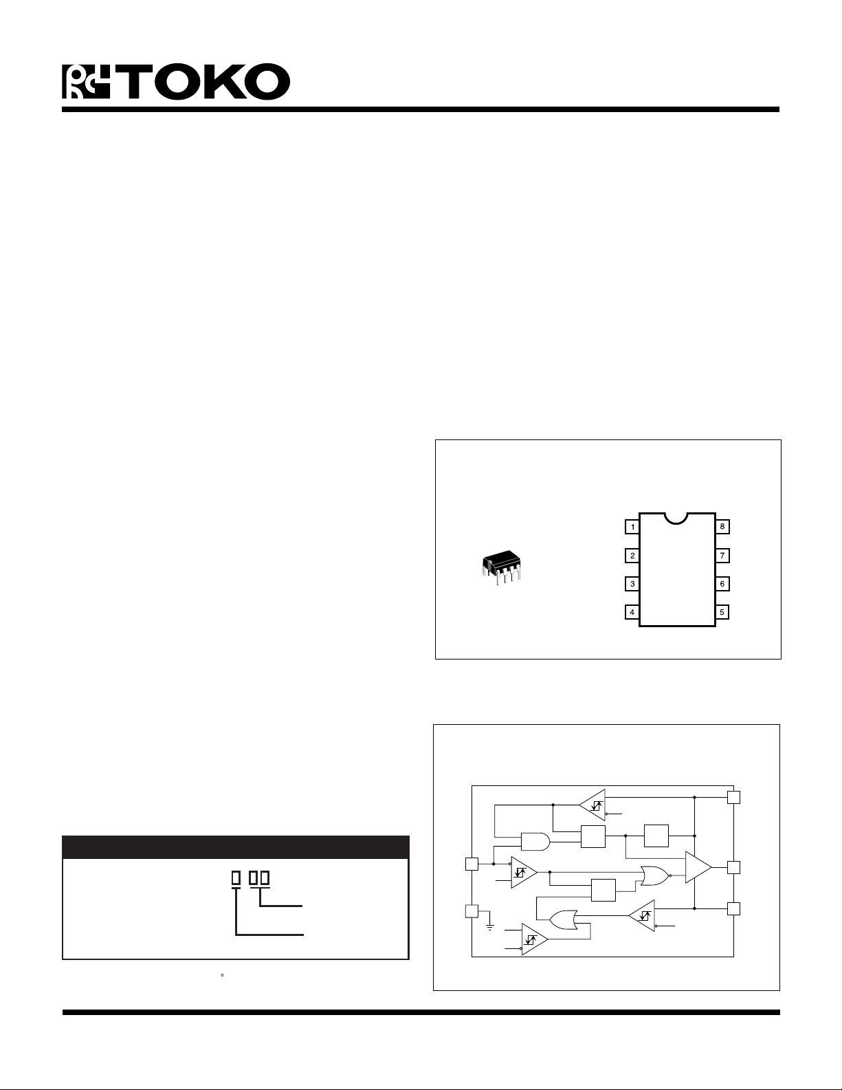
The TK75050 is a non-inverting buffer to drive high power
insulated gate transistors (e.g., MOSFETs and IGBTs).
The output can source or sink 2 A into a 10,000 pF
equivalent load. The IC features built-in cycle-by-cycle
current limiting. Its Undervoltage Lockout (UVLO) circuit is
combined with a First Pulse Wake-up Feature*. The chip
has thermal overload protection. Using the IC in the Gate
Charge Recovery* application, the switching spike
developed across the current sense resistor practically
becomes negligible. Due to its low standby current and
first-pulse wake-up feature, the device can be used in selfbiased power supplies. The IC's high-speed cycle-bycycle current limiting capability eliminates the short circuit
runaway problem which characterizes most currentcontrolled converters. The IC is well suited to provide
supplementary overload protection in voltage-controlled
converters, too. The TK75050 is available in the widely
used 8-pin DIP package.
*Toko proprietary feature: See "Application Information" section.
TK75050
SMART MOSFET DRIVER
APPLICATIONS
■ Driving of Power MOSFETs and IGBTs
■ Switch Mode Power Supplies
■ Step Motor Drivers
■ Solenoid Drivers
TK75050
PGND/CS
75050
BLOCK DIAGRAM
GND
GND
OUTPUT
INPUT
GND
GND
V
CC
ORDERING INFORMATION
PACKAGE CODE
D: DIP-8
TK75050D
EXTENDED TEMP. RANGE
I: -40 TO +85 C
Tape/Reel Code
Temperature Code
TAPE/REEL CODE
TL: Tape Left
INPUT
GND
1.6/1.0 V
155/80 °C
UVLO
Q
R
Q
S
CURRENT
OVERLOAD
11/10 V
EN
BIAS
EN
1.0/0.9 V
STARTUP
R
S
OVERLOAD
T
THERMAL
OVERLOAD
V
CC
OUTPUT
PGND/CS
January 1999 TOKO, Inc. Page 1
Page 2
TK75050
ABSOLUTE MAXIMUM RATINGS
Supply Voltage (Low Impedance Source)................ 14 V
Power Dissipation TK75050D (Note 1) .............. 825 mW
Storage Temperature Range ................... -55 to +150 °C
Operating Temperature Range ...................-20 to +70 °C
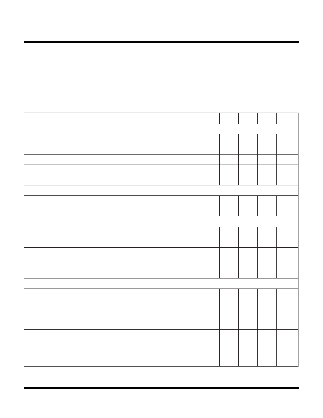
TK75050 ELECTRICAL CHARACTERISTICS
Test conditions: V
LOBMYSRETEMARAPSNOITIDNOCTSETNIMPYTXAMSTINU
= 12 V, T
CC
= Tj = Full Operating Temperature Range, DC Test Setup 1, unless otherwise specified.
A
NOITCESYLPPUSREWOP
Extended Temperature Range................... -40 to +85 °C
Junction Temperature .......................................... 150 °C
Lead Soldering Temperature (10 s) ..................... 235 °C
I
)YBTS(CC
I
)L(CC
I
)H(CC
I
)DS(CC
I
SC/DNGP
tnerruCylppuS
tnerruCylppuS
tnerruCylppuS
tnerruCyppuS
)ybdnatS(
tnerruCSC/DNGP
)2etoN(,V
)WOLtuptuO(
)HGIHtuptuO(
NI
V
NI
V
NI
)NWODTUHStuptuO(
)WOLtuptuO(
V
NI
pU-ekaWerofeBV0=0550001Aµ
pU-ekaWretfAV0=7162Am
pu-ekaWretfAV4.2=4181Am
daolrevOlamrehTrotnerruC9142Am
pu-ekaWretfAV0=401Am
NOITCESTUOKCOLEGATLOVREDNU
V
)NO(CC
V
)FFO(CC
egatloVyppuS
egatloVyppuS
)dlohserhTHGIHOLVU(
V
CC
)dlohserhTWOLOLVU(
V
CC
drawpUspeewS4.010.114.11V
drawnwoDspeewS3.90.014.01V
NOITCESTUPNI
V
)L(NI
V
)H(NI
I
)L(NI
I
)H(NI
V
)UW(NI
egatloVtupnI
egatloVtupnI
tnerruCtupnI
)WOL(
tnerruCtupnI
)HGIH(
egatloVtupnI
)dlohserhTWOL(
)dlohserhTHGIH(
V
V
V0=052-001-Aµ
NI
NI
V4.2=0152Aµ
)dlohserhTpu-ekaW(
6.00.1V
6.11.2V
5.052.152.2V
NOITCESTUPTUO
I
V
)L(TUO
egatloVtuptuO
)WOL(
KNIS
I
KNIS
I
V
)H(TUO
I
)XAM(TUO
I
)YBTS(TUO
egatloVtuptuO
)HGIH(
I
ecruoSrokniStuptuOmumixaM
)3etoN(,tnerruC
C
L
tnerruCnwod-lluPtuptuOybdnatSV
CC
Am05=52.05.0V
A0.1=0.38.3V
ECRUOS
ECRUOS
Am05=7.95.01V
A0.1=0.85.9V
Fp000,01=0.2A
V9=
V
V
V8=15.2Am
TUO
V2=3.07.0Am
TUO
Page 2 January 1999 TOKO, Inc.
Page 3

TK75050 ELECTRICAL CHARACTERISTICS (CONT.)
Test conditions: V
LOBMYSRETEMARAPSNOITIDNOCTSETNIMPYTXAMSTINU
= 12 V, T
CC
= Tj = Full Operating Temperature Range, DC Test Setup 1, unless otherwise specified.
A
NOITCESNOITCETORPDAOLREVOLAMREHT
TK75050
lamrehT,erutarepmeTnoitcnuJ
T
)FFO(j
,dlohserhTnwodtuhSdaolrevO
)3etoN(
T
)NO(j
otkcaBnruT,erutarepmeTnoitcnuJ
)3etoN(,dlohserhTedoMlamroN
speewSerutarepmeT
edoMlamroNnidrawpU
edoMnwodtuhSlamrehTni
NOITCESNOITCETORPDAOLREVOTNERRUC
V
LC
V
)TSYH(LC
dlohserhTtimiL
tnerruC,egatloVesneStnerruC
tnerruC,egatloVesneStnerruC
)3etoN(,siseretsyHtimiL
V
SC
T
A
,drawpUspeewS
2puteStseTCD,C°52=
2puteStseTCD001Vm
SCITSIRETCARAHCGNIHCTIWS
t
RD
t
R
t
FD
t
F
t
)SOC(D
Note 1: Power dissipation is 825 mW when mounted. Derate at 6.6 mW/°C for operation above 25°C.
Note 2: Conditions for "wake-up": either 1) VIN exceeds V
or 2) VCC exceeds V
Conditions for "standby": either 1) VCC never exceeds V
or 2) VCC drops below V
or 3) VIN never exceeds V
Note 3: Guaranteed by design; not 100% tested.
emiTyaleD
emiTesiRC
emiTyaleD
emiTllaFC
)ESIR(
)LLAF(
daolrevOtnerruC,emiTyaleD
)3etoN(,nwodtuhS
C
L
L
C
L
L
C
L
, stays above V
IN(H)
, stays above V
CC(ON)
CC(ON)
CC(OFF)
IN(H)
,Fp0001= ∆V
SC
,Vm002=
3puteStseTCA
, and VCC passes V
IN(L)
.
, and VIN exceeds V
CC(OFF)
051C°
drawnwoDspeewSerutarepmeT
08C°
8.059.01.1V
3puteStseTCA,Fp0001=0254sn
3puteStseTCA,Fp0001=0204sn
3puteStseTCA,Fp0001=0254sn
3puteStseTCA,Fp0001=0204sn
021sn
CC(ON)
IN(H)
.
January 1999 TOKO, Inc. Page 3
Page 4
TK75050
TEST CIRCUITS
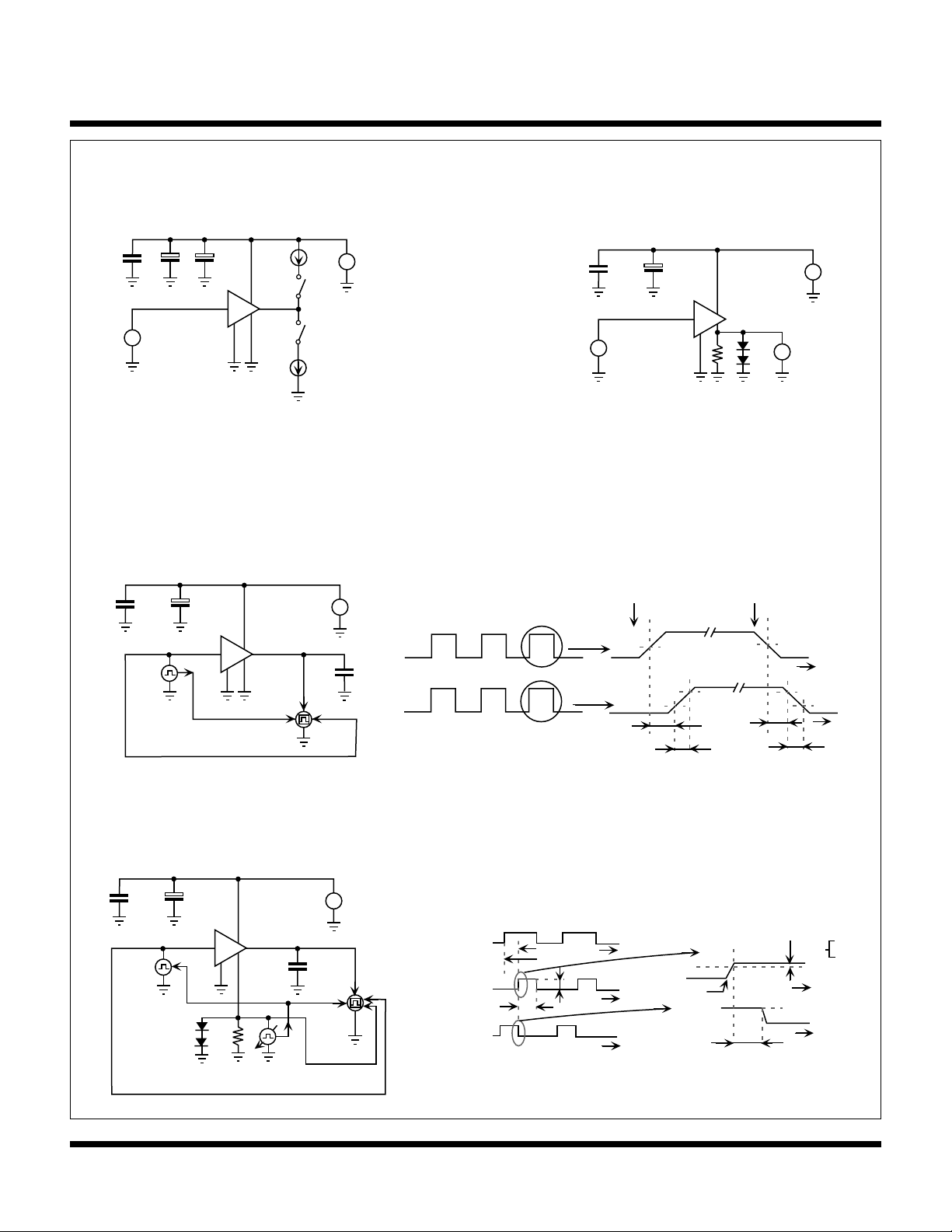
DC TEST SETUP 1
+
+
100 nF
10 µF 10000 µF
V
CC
IN
+
V
IN
-
GND
OUT
PGND/CS
I
SINK
SW
2
SW
1
I
SOURCE
+
V
CC
-
Note: SW1 and SW2 are open by default. To avoid excessive
dissipation, they are exclusively closed only for less than 100 ms to
measure the appropriate output voltages V
specified currents I
SOURCE
and I
, respectively.
SINK
OUT(H)
and V
OUT(L)
at
AC TEST SETUP 3
+
100 nF
V
IN
GENERATOR
PULSE
10 µF
SYNCH
IN
GND
V
CC
PGND/CS
OSCILLOSCOPE
OUT
TRIG
Ch A
Ch B
+
-
V
CC
1000 pF
C
L
V
IN
ZOOM IN
ZOOM IN
DC TEST SETUP 2
+
100 nF
+
-
10 µF
V
CC
IN
GND
+TRIG -TRIG
1.6 V
90 %
10 %
t
DR
t
R
PGND/CS
10
+
V
CC
-
+
V
CS
-
1.0 V
t
90 %
10 %
t
DF
t
t
F
AC TEST SETUP 4
100 nF
VIN (t)
f = 10 kHz
D = 1:1
Level = TTL
GENERATOR
PULSE
+
10 µF
TRIG IN
1
GND
V
CC
IN
OUT
PGND/CS
VCS (t)
10 Ω
PULSE
GENERATOR
RS ≤ 50 Ω
V
C
L
1000 pF
TRIG IN
SYNCH OUT
f = 10 kHz
D = 1:10
Level = ADJ.
2
OUT
Ch A
+
V
CC
-
(t)
Ch B
OSCILLOSCOPE
Ch C
VIN (t)
+TRIG
V
(t)
CS
V
(t)
OUT
tD = 10 µs
T = 100 µs
V
CS
tW = 10 µs
ADJ
t
ZOOM IN
t
ZOOM IN
t
+TRIG
V
OUT(H)
V
OUT(L)
VCL = 1 V
t
D(COS)
t
90 %
t
VCS =
50 mV
200 mV
Page 4 January 1999 TOKO, Inc.
Page 5
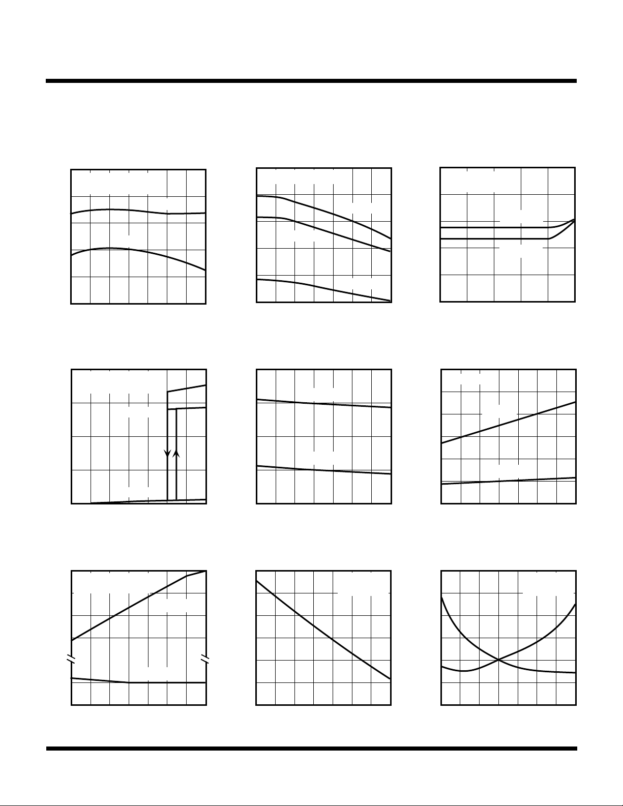
TYPICAL PERFORMANCE CHARACTERISTICS
I
(
A)
I
(
A)
I
(
A)
I
(
A)
INPUT
THRESHOLD
(V)
V
(V)
V
(V)
RISE AND FALL TIME
VS.
TEMPERATURE
TA (°C)
-25 25 75 125
TIME (ns)
28
15
24
20
V
CC
= 12 V
CL = 1000 pF
t
F
t
R
TK75050
SUPPLY CURRENT VS.
TEMPERATURE
20
VCC = 12 V
NO LOAD CONNECTED
m
CC
18
16
14
I
CC(H)
I
CC(L)
12
10
-25 25 75 125
TA (°C)
SUPPLY CURRENT VS.
SUPPLY VOLTAGE
20
TA = 25 °C
NO LOAD CONNECTED
15
ACTIVE MODE
m
10
CC
5
0
SLEEP MODE
2 6 10 14
V
(V)
CC
STANDBY CURRENT VS.
TEMPERATURE
700
NO LOAD CONNECTED
600
µ
500
VCC = 10 V
400
CC(STBY)
300
200
-25 25 75 125
TA (°C)
UVLO THRESHOLD
TEMPERATURE
11.5
V
CC(ON)
11.0
10.5
V
CC(OFF)
10.0
UVLO THRESHOLD (V)
9.5
-25 25 75 125
TA (°C)
VCC = 12 V
VCC = 5 V
VS.
AVERAGE SUPPLY CURRENT VS.
FREQUENCY
20
VCC = 12 V
NO LOAD CONNECTED
18
m
16
14
CC(AVG)
TA = 25 °C
TA = 125 °C
12
10
0.01 0.1 1 10 100 1000
FREQUENCY (kHz)
INPUT THRESHOLD
VS.
TEMPERATURE
2.0
V
= 12 V
CC
V
1.6
1.2
0.8
-25 25 75 125
IN(H)
V
IN(L)
TA (°C)
OUTPUT VOLTAGE VS.
TEMPERATURE
10.8
V
= 12 V
CC
NO LOAD CONNECTED
10.6
10.4
10.2
OUT
0.2
0.0
-25 25 75 125
January 1999 TOKO, Inc. Page 5
V
OUT(L)
TA (°C)
V
OUT(H)
CURRENT LIMIT THRESHOLD VS.
TEMPERATURE
1.2
1.0
CL
0.8
0.6
-25 25 75 125
TA (°C)
V
CC
VIN = V
= 12 V
IN(H)
Page 6
TK75050
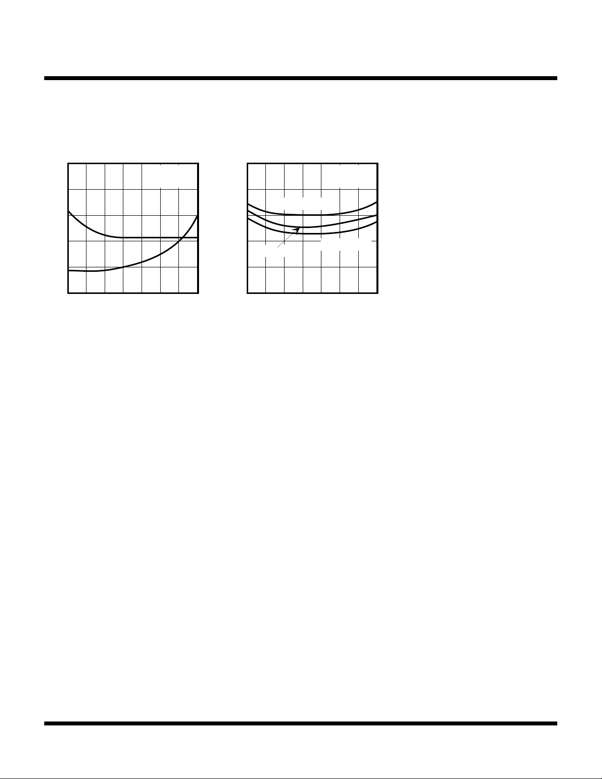
PROPOGATION
DELAY
(
)
PROPOGATION
DELAY
(
)
TYPICAL PERFORMANCE CHARACTERISTICS (CONT.)
PROPOGATION DELAY
TEMPERATURE
36
ns
32
28
t
DF
24
t
DR
20
16
-25 25 75 125
TA (°C)
VS.
V
= 12 V
CC
CL = 1000 pF
CURRENT OVERLOAD SHUTDOWN
DELAY
VS.
TEMPERATURE
250
ns
200
∆VCS = 50 mV
150
100
∆VCS = 100 mV
∆VCS = 200 mV
50
0
-25 25 75 125
TA (°C)
V
= 12 V
CC
CL = 1000 pF
Page 6 January 1999 TOKO, Inc.
Page 7

PIN DESCRIPTION
TK75050
SUPPLY VOLTAGE PIN (VCC)
This pin is connected to the supply voltage. Regardless of
the state of the other pins, the IC is always in a low-current
standby mode when the supply voltage is below the lower
threshold of the undervoltage lockout circuit. The IC enters
normal mode when two conditions are met simultaneously:
1) the supply voltage exceeds the upper threshold of the
undervoltage lockout circuit, and 2) a "first" pulse arrives at
the input.
That first pulse "wakes up" the IC ( i.e., it enables the highspeed internal circuitry). The First Pulse Wake-Up is a
proprietary feature of theTK75050. The feature is
proprietary, but use is granted for use with the IC. That
feature is indispensable in off-line self-biased powersupply applications where the start-up current is provided
by a large-value resistor connected between the rectified
line and the IC (see Figure 1). Without the First Pulse
Wake-up, the starting current would be equal to the normal
supply current, which is prohibitively large for a self-biased
start.
GROUND PIN (GND)
1.3 V. The hysteresis ensures that noise riding on the input
signal does not cause spurious response at the output.
POWER GROUND/CURRENT SENSE PIN (PGND/CS)
This pin has two distinct functions: 1) it provides a separate,
fully floating return path for the turnoff drive current of the
output stage and, thus, reduces the internal noise of the IC;
2) by connecting the pin to a current-sense resistor, the IC
acts as a fast cycle-by-cycle current limiter.
When the voltage between the power-ground pin (PGND/
CS) and the signal-ground pin (GND) exceeds the 0.95 V
current-limit threshold, the drive signal is terminated for
the remainder of the time while the input signal is high.
Once the input signal returned to zero, the latch that stored
the information about the presence of the overcurrent is
reset, and the IC is ready to acquire another overcurrent
event in the next cycle.
This pin provides ground return connection for the smallsignal portion of the IC. The return of the output stage is not
connected here, but to the floating power GND pin.
OUTPUT PIN
This pin drives the external MOSFET using a totem pole
output stage. The peak drive source or sink current is
typically 2 A into a 10,000 pF equivalent load. The UVLO
circuity ensures that the high-level output voltage will
never be less than about 7 V. In standby mode, the output
stage is equivalent to a pull-down resistor of about 3 kΩ
value, eliminating the need for an external gate to source
resistor. Normally, there is no need to add a Schottky diode
between the output and ground. In applications, however,
with heavy capacitive load located far from the IC or when
the IC drives a transformer, the Schottky diode may
become necessary.
INPUT PIN
The input pin receives the signal to be buffered. The
incoming signal is processed by a comparator with a
600 mV hysteresis centered around a threshold of about
January 1999 TOKO, Inc. Page 7
Page 8
TK75050
APPLICATION INFORMATION
START-UP
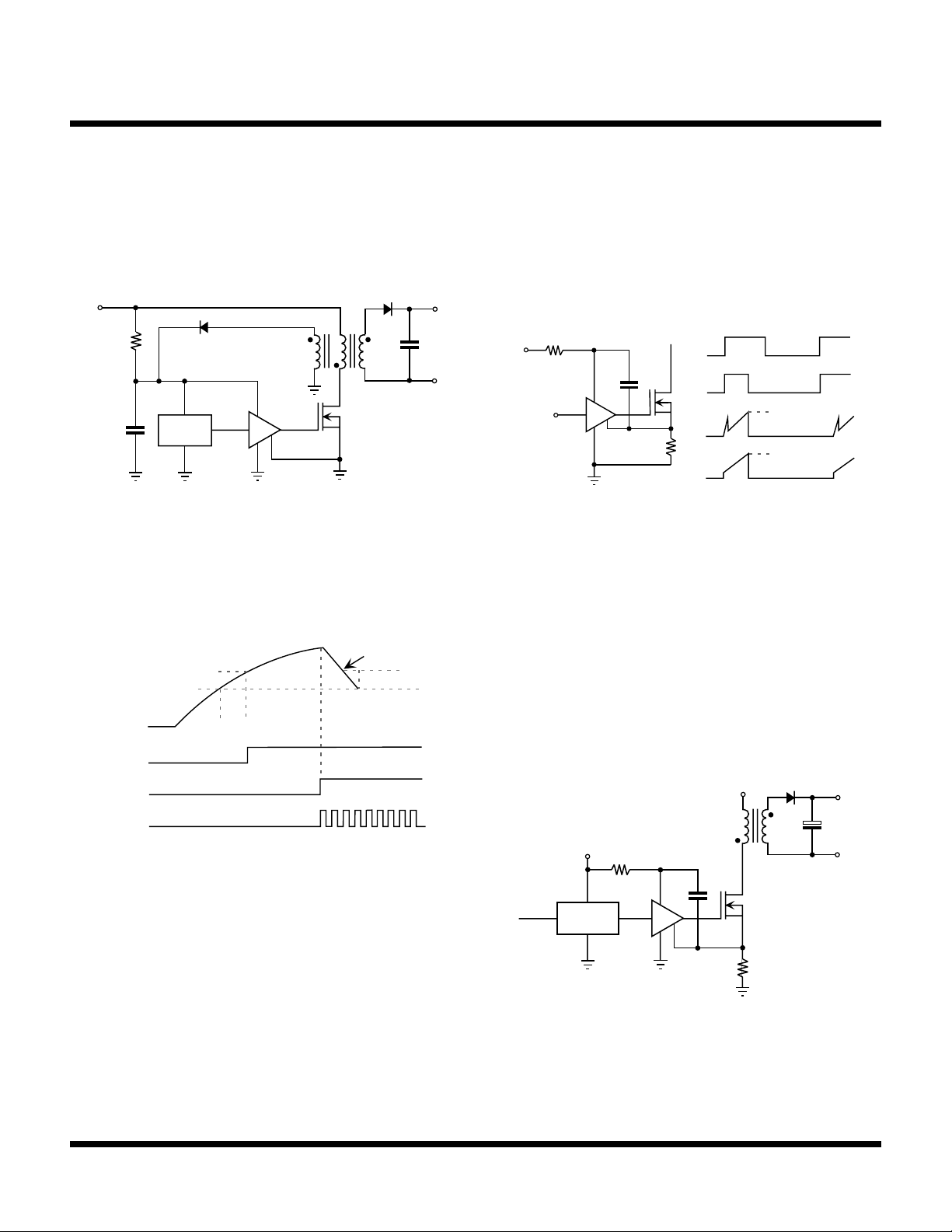
Figure 1 shows the application of the TK75050 smart
MOSFET driver in a self-biased power supply.
V
IN
+
V
CC
TK75050
+
PWM
CONTROLLER
FIGURE 1: TK75050 IN A SELF-BIASED POWER
SUPPLY
Figure 2 shows the typical waveforms during start-up.
PWM ENABLE
BOOTSTRAP REGULATION
UVLO UPPER THRESHOLD
UVLO LOWER THRESHOLD
V
(t)
CC
V
(t)
UVLO
V
(t)
IN
V
(t) & V
OUT
(t)
IN
UVLO
CONDITION
FIRST PULSE
CONDITION
DRIVER “WAKES UP”
BEGINS
granted for use with the TK75050. For a detailed description
and application information of the Gate Charge Recovery
technique, see the Toko application note "Application
Considerations for a Smart Five-Pin MOSFET/IGBT Driver
with High-Speed Current-Limit Capability."
V
AUX
R
F
C
F
V
CC
GND
OUT
PGND/CS
VCS (t)
IN
IN
OUT
0.95 V
VCS(t)
+
R
CS
-
VCS(t)
CF IS CONNECTED TO GND
0.95 V
CF IS CONNECTED TO PGND/CS
(a) (b)
FIGURE 3: CYCLE-BY-CYCLE CURRENT LIMIT WITH
THE TK75050
(a) SCHEMATIC (b) WAVEFORMS
MAIN OVERLOAD PROTECTION IN VOLTAGEMODE-CONTROLLED CONVERTERS
Figure 4 shows the TK75050 in a voltage-mode-controlled
flyback converter. In this application example, the IC
provides the main overload protection.
V
IN
+
+12 V
FIGURE 2: WAVEFORMS DURING START-UP
FEEDBACK
CYCLE-BY-CYCLE CURRENT LIMIT
VOLTAGE-MODE
PWM
CONTROLLER
Figure 3(a) shows how to use the TK75050 as a highspeed cycle-by-cycle current limiter. Figure 3(b) shows the
waveforms. Note that the preferred connection for the
bottom terminal of the filter capacitor CF is to the PGND/CS
pin and not to the GND pin. By connecting CF to the PGND/
FIGURE 4: TK75050 IN A VOLTAGE-MODE-
CONTROLLED CONVERTER
CS pin, the capacitive feedthrough of the drive signal that
would appear as a leading-edge spike in the current-sense
waveform is completely eliminated. This technique, called
"Gate Charge Recovery" is patented by Toko, Inc., but is
Page 8 January 1999 TOKO, Inc.
Page 9
APPLICATION INFORMATION (CONT.)
+
V
IN
+12 V
+
-
+-FEEDBACK
TK75050
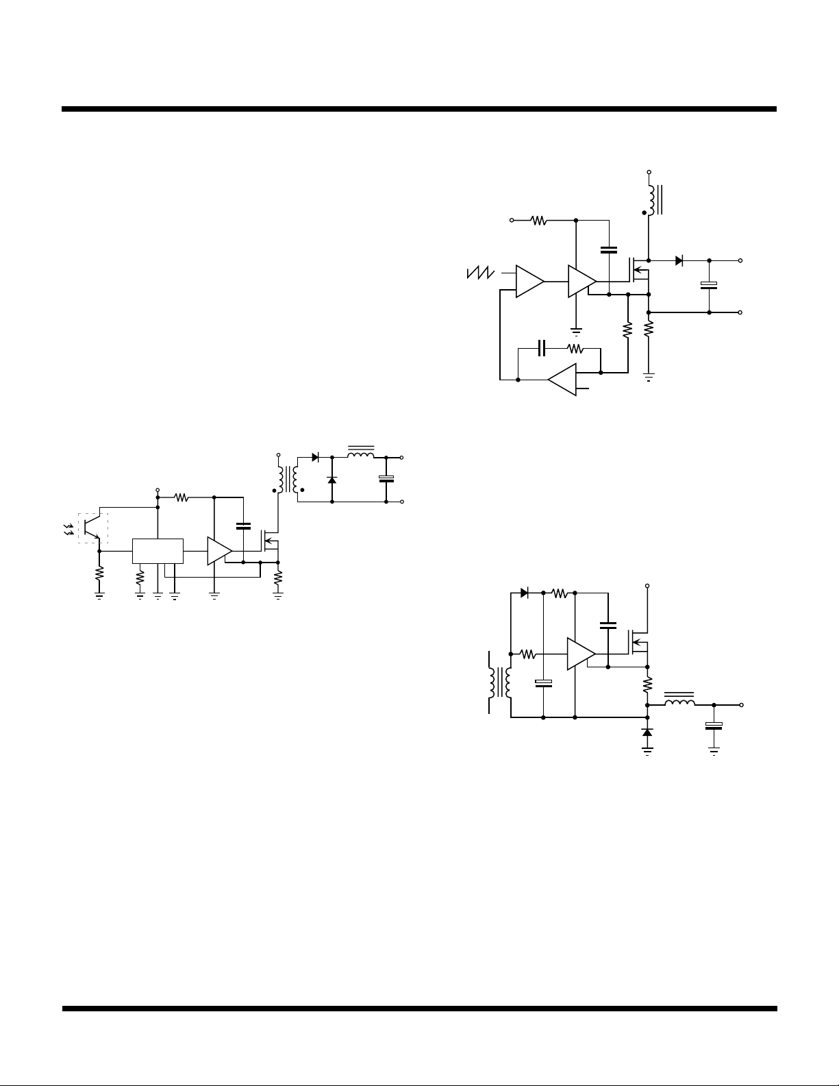
ADDITIONAL OVERLOAD PROTECTION IN PEAKCURRENT-CONTROLLED CONVERTERS
Figure 5 shows the TK75050 in a current-mode-controlled
forward converter, with optically isolated feedback. In this
application the TK75050 helps to achieve a tightly controlled
current-limit-characteristic. A tight current limit cannot
usually be achieved with only current-mode control due to
the presence of the stabilizing ramp. The lack of the
stabilizing ensures that the knee current (i.e., the output
current where the limiting begins) is only slightly lower than
the short-circuit current. The difference between the knee
current and the short-circuit current is about one-half of the
ripple current in the filter inductor. If a stabilizing ramp were
added to the current-sense signal, the difference would be
significantly higher.
V
IN
+12 V
OC
TK75050
CURRENT-MODE
PWM
CONTROLLER
+
TK75050
FIGURE 6: TK75050 IN A CONVERTER WITH
AVERAGE CURRENT CONTROL
FLOATING DRIVE WITH OVERLOAD PROTECTION
The TK75050 can be used as a driver and current limiter
for a floating power switch. Figure 7 shows the IC in a buck
converter with transformer-isolated drive.
FIGURE 5: TK75050 IN A PEAK-CURRENT-
CONTROLLED CONVERTER
ADDITIONAL OVERLOAD PROTECTION IN AVERAGECURRENT-CONTROLLED CONVERTERS
In converters with average current control the peak current
information is lost and the response of the current-control
loop slows down. The speed of the current-control loop
may not be sufficient to provide effective protection against
sudden overload or saturation of an inductor or transformer.
Figure 6 shows an average-current-controlled boost
converter where the TK75050 provides additional fast
overload protection.
V
IN
+
TK75050
FIGURE 7: TK75050 AS A FLOATING DRIVER IN A
BUCK CONVERTER
DEMO BOARD
The purpose of the board is to demonstrate the high-speed
current-limit capability of Toko's TK75050 smart MOSFET
driver. In the board a 2-A/500 V MOSFET switch is turned
on directly (i.e., without any series impedance) into a DCbus with up to 400 V, at a frequency of 30 kHz. By removing
the short across a 3.3 µH inductor in series with the
MOSFET, it is also possible to investigate the effect of the
wiring inductance between the switch and the load. In
January 1999 TOKO, Inc. Page 9
Page 10
TK75050
APPLICATION INFORMATION (CONT.)
addition to the short-circuit protection, the board also illustrates how to use the IC for driving and protecting a floating
switch.
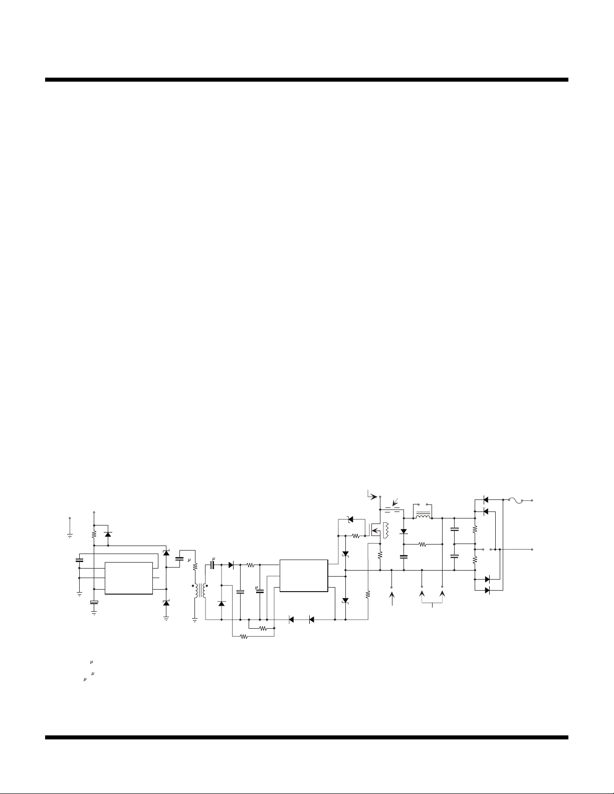
CIRCUIT SCHEMATIC
Figure 8 shows the circuit schematic. The operation is as follows: U1, a 5-pin PWM IC (TK75001) generates a 30 kHz
square-wave signal, with about 15 V peak-to-peak magnitude and 44% duty ratio. That square-wave signal is connected
to the primary winding of a pulse transformer T1 through a coupling capacitor C9 and a small series resistor R11. A voltagedoubler comprising C3, C4, D3 and D4 rectifies the transformed square wave appearing across the secondary winding of
the transformer, generating a floating supply voltage of about 12 V for the MOSFET driver IC U2 (TK75050). A drive signal
is derived for U2 from the voltage across the diode D4 with the help of the resistive divider R3 and R2. The output of U
(pin 3) is connected to the gate of the MOSFET Q1 through a 150 ohm resistor R4 and a parallel diode D5. The current
of the MOSFET switch is sensed by resistor R5. D6 and D7 protect the PGND/CS pin (pin 1) of U2 from excessive voltage;
D8 and D9 prevent the voltages of pins 3 and 1 from swinging below ground by more than 0.3 V. The MOSFET Q1 is
connected to a DC-bus through a small inductor L1. That inductor represents the inductance of a wire connection to a
load, which is at a distance of approximately 1 meter from the MOSFET. By placing a short across jumper JP1, we can
emulate the case when the free-wheeling diode in a buck or boost converter fails. If the inductor L1 is not shorted, a clamp
comprising D10, C6 and R7 limits the drain voltage excursion of Q1 to about 60 V above the bus voltage.
2
A test loop is provided for clamp-on type current probes to monitor the current in the MOSFET Q1. Test points TP1 through
TP4 are available for measuring the dc bus voltage and the voltage across Q1.
The DC-bus is generated by rectifying the line voltage with a bridge rectifier (in the case of 230 V
doubler (in the case of 115 V
line, when jumper JP2 is shorted). Alternatively, a DC source of not more than 400 V
RMS
line) or with a voltage
RMS
can be connected to the line terminals.
Notes: (1) Leave JP2 open if you connect more than 250 V dc voltage to the line terminals, otherwise the excess voltage across C7 or C8 can lead
to failure of the capacitor. (2) Never operate the circuit from 230 V
that will destroy capacitor C7 and C8 and transistor Q1.
+15 V
TP
5
R
10
1 k
C
2
1.5 n
+
Q1: IRF820 (IR PREFERRED)
HS1: HS121-ND (DIGI-KEY, AAVID)
D1, D2, D5, D8, D9: 1N5817
D3, D4, D6, D7: 1N4148
D10: BYV26C
D
: 1N4005
12-15
C1, C4: 10
, 25 V
C6: 15 n, 630 V(e.g. ECQ-E6153KF, PANASONIC)
C7, C8: 2.2
, 250 V (PANASONIC SU SERIES, RADIAL, ECE-A2EU2R2)
L1: 3.3.
, 4 A (e.g. R622LY-3R3M, TOKO)
T1: RM5/i, 3E1 (PHILIPS), n1 = 40, n2 = 46, SINGLE LAYER WINDINGS, WIRE SIZE TO FILL THE BOBBIN
MYLAR INSULATION BETWEEN LAYERS, FOR 1 kV BETWEEN PRIMARY AND SECONDARY
JP2: OPEN AT 230 V, SHORTED AT 115 V.
1N5226B (3.3 V)
FB
GND
V
CC
C
1
D
11
U
1
TK75001
GND
DRV
D
2
C
T
D
1
C
3
C
9
1
R
11
10
n
1
T
D
3
1
n
2
1
R
1
10
C
5
+
0.1
C
4
D
4
R
3
22 k
line with the jumper JP2 shorted. In such a case excess bus voltage will develop
RMS
TEST LOOP
FOR CURRENT
TEST POINT FOR VOLTAGE OBSERVATION
U
2
TK75050
10 k
V
CC
GND
IN
R
2
D7D
OUT
GND
PGND/CS
6
D
5
R
150
D
8
D
9
TP
4
4
PROBE
Q
1
HS
1
R
5
0.47
1 W
TP
R
6
10
TEST POINT FOR
SCOPE GND CLIP
JP
D
10
R
1 k
1 W
C
6
3
VCC MEASUREMENT
1
L
1
7
TP
TP
1
TEST POINTS FOR
(MAX. 400 VDC)
D
12
D
15
R
9
C
7
1 M
JP
2
C
R
8
8
1 M
D
14
D
2
13
F
1
1A SLOW
115 OR 230
Vrms
FIGURE 8: CIRCUIT SCHEMATIC
Page 10 January 1999 TOKO, Inc.
Page 11
APPLICATION INFORMATION (CONT.)
TK75050
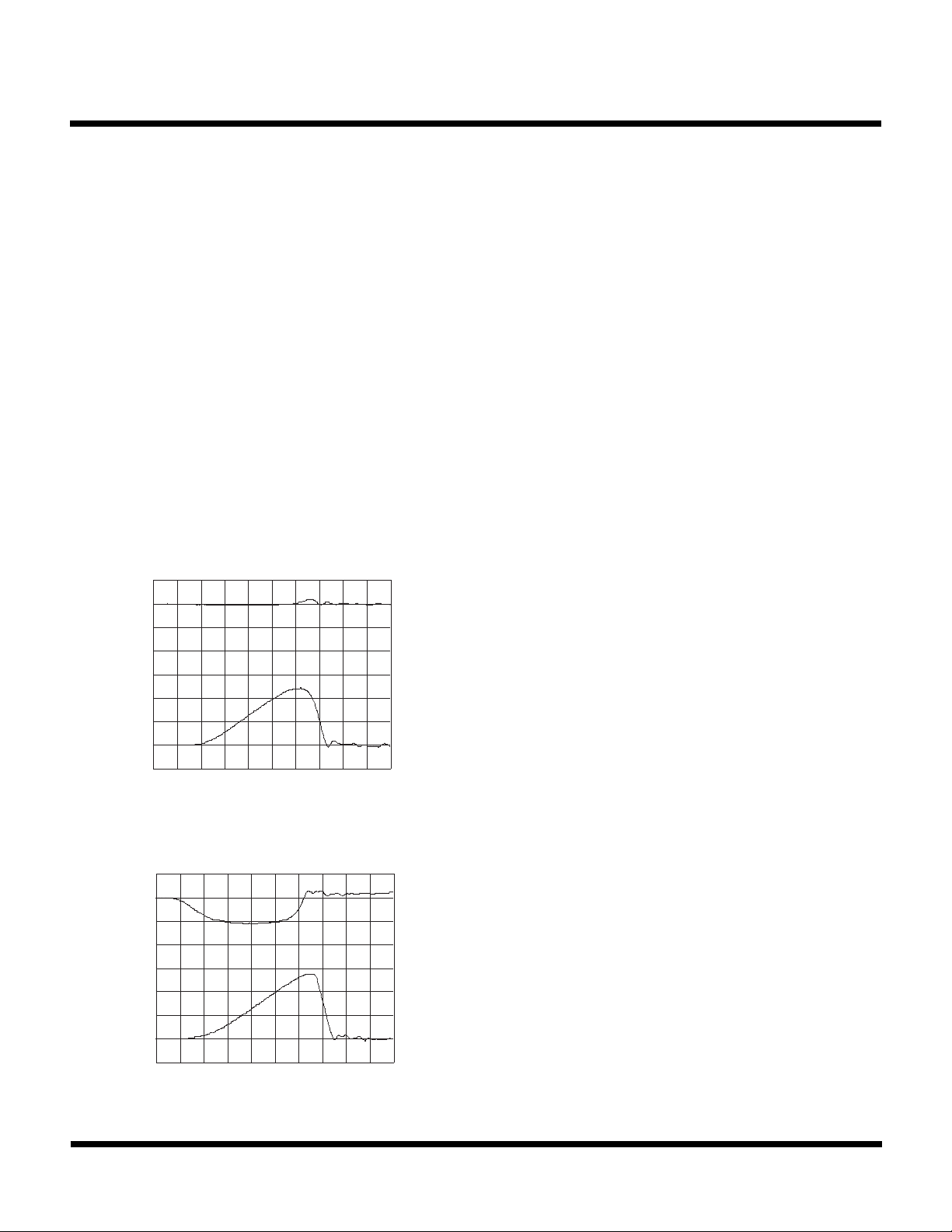
Figures 9 and 10 show the measured voltages across Q
(top trace) and the currents in Q1 (bottom trace). Figure 9
shows the wave forms when there is no inductor in series
with Q1 (i.e., L1 is shorted). Figure 10 shows the waveforms
when there is an inductor in series with Q1 (i.e., L1 is not
shorted). The vertical scales are 100 V/div. (top trace) and
1 A/div (bottom trace). The horizontal scales are 25 ns/div.
As can be seen, the peak currents stay below 2.5 A
(Figure 9) or 2.8 A (Figure 10). Those numbers correspond
to 25% or 40% overshoots above the nominal current-limit
threshold of 2 A. Both figures show that the IC shuts off the
MOSFET completely in less than 50 ns after the current
passed the 2 A threshold. The measured average DC
current consumption at a bus voltage of 400 V and a
switching frequency of 30 kHz is 4.3 mA when L1 is shorted
(Figure 9) and 5.3 mA when L1 is not shorted (Figure 10).
400V
SAFETY CONSIDERATIONS/LIABILITY DISCLAIMER
1
Dangerous voltages are present in the demo board.
Extreme caution must be used when using and testing the
circuit. Only trained personnel, experienced in working
with high voltages and power, should operate it. Use an
isolating transformer between the line and the circuit if any
grounded instrument (including the 20 V auxiliary supply
for the square-wave generator at the primary side of
transformer T1) is to be connected to the board. Note:
Although the two windings of transformer T1 are isolated
from each other, the transformer is not designed to provide
safety isolation between those windings.
Toko, Inc. disclaims any and all liability arising from use or
misuse of the demo board described herein.
400V
0V
25ns/div.
2A
0A
FIGURE 9
0V
25ns/div.
2A
0A
FIGURE 10
January 1999 TOKO, Inc. Page 11
Page 12
TK75050
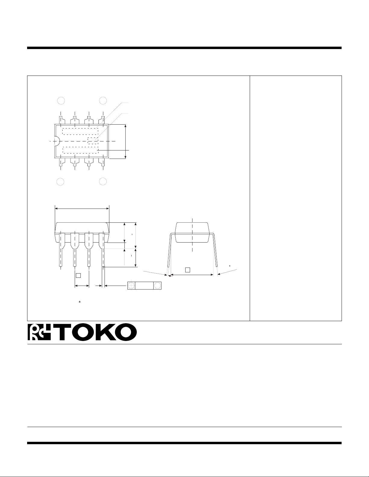
PACKAGE OUTLINE
DIP-8
Marking Information
8
1
9.5
e
2.54
5
4
0.46
+ 0.15
- 0.05
Marking
Lot Number
6.4
Country of Origin
0.3
+
3.3
0.3
+
0.5 min
Marking
TK75050 75050
3.8
3.3
0.25
0.25
+ 0.15
- 0.05
e1
7.62
M
0 ~15
Dimensions are shown in millimeters
Tolerance: x.x = 0.2 mm (unless otherwise specified)
Toko America, Inc. Headquarters
1250 Feehanville Drive, Mount Prospect, Illinois 60056
Tel: (847) 297-0070 Fax: (847) 699-7864
TOKO AMERICA REGIONAL OFFICES
Midwest Regional Office
Toko America, Inc.
1250 Feehanville Drive
Mount Prospect, IL 60056
Tel: (847) 297-0070
Fax: (847) 699-7864
Western Regional Office
Toko America, Inc.
2480 North First Street , Suite 260
San Jose, CA 95131
Tel: (408) 432-8281
Fax: (408) 943-9790
Eastern Regional Office
Toko America, Inc.
107 Mill Plain Road
Danbury, CT 06811
Tel: (203) 748-6871
Fax: (203) 797-1223
Semiconductor Technical Support
Toko Design Center
4755 Forge Road
Colorado Springs, CO 80907
Tel: (719) 528-2200
Fax: (719) 528-2375
Visit our Internet site at http://www.tokoam.com
The information furnished by TOKO, Inc. is believed to be accurate and reliable. However, TOKO reserves the right to make changes or improvements in the design, specification or manufacture of its
products without further notice. TOKO does not assume any liability arising from the application or use of any product or circuit described herein, nor for any infringements of patents or other rights of
third parties which may result from the use of its products. No license is granted by implication or otherwise under any patent or patent rights of TOKO, Inc.
Page 12 January 1999 TOKO, Inc.
All Rights Reserved
IC-164-TK75050
0798O0.0K
Printed in the USA© 1999 Toko, Inc.
 Loading...