

Page 1
TK75003
75003
PWM CONTROLLER
FEATURES
■ Power Factor Correction/Line Harmonics
Reduction to Meet IEC1000-3-2 Requirements
■ Optimized for Off-Line Operation
■ Maximum Duty Ratio 88% (typ.)
■ Frequency Reduction for Improved Overcurrent
Protection
■ Low Standby Current for Current-Fed Start-Up
■ Current-Mode or Voltage-Mode Control
■ Internal User-Adjustable Slope Compensation
■ Functionally Integrated & Simplified 5-Pin Design
DESCRIPTION
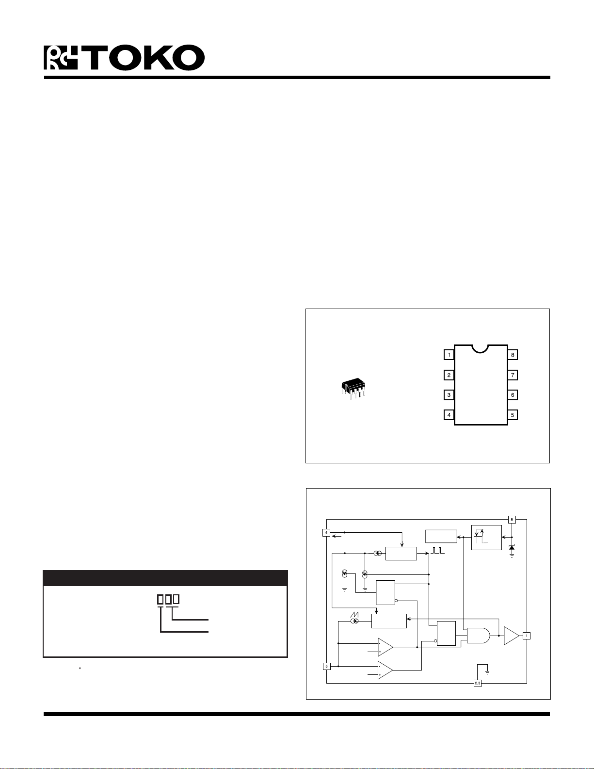
The TK75003 is a simple primary side controller optimized
for off-line switching power supplies including power factor
correctors. It is suitable for both voltage-mode and currentmode control and has advanced features not available in
controllers with a higher pin count. The key to full
functionality in a 5-pin design is that the current signal and
the error signal are added together and fed into the
feedback pin. A sawtooth current flowing out of the feedback
pin provides a slope compensation ramp (in current-mode
applications) or a PWM ramp (in voltage-mode
applications), in proportion to the resistance terminating
that pin. If the sum of the current sense signal, error signal
and ramp signal exceeds the Overcurrent Detector
threshold indicating that the Current Control Detector has
lost control of the switch current, the charging current of
the timing capacitor will be reduced to about 25% for the
remainder of the clock period. The reduced charging
current causes no more than a one-third reduction in
switching frequency, effectively preventing short-circuit
current runaway.
ORDERING INFORMATION
TK75003D
Tape/Reel Code
Temperature Code
TEMP. CODE (OPTIONAL)
I: -40 to +85 C
TAPE/REEL CODE
MG: Magazine
APPLICATIONS
■ Power Factor Correction Converters
■ Off-Line Power Supplies
■ Industrial Power Supplies
■ Telecom Power Supplies
■ Off-Line Battery Chargers
TK75003
DRV
GND NC
GND
T
Note: Pins 2 and 3 must be externally
connected for proper operation.
BLOCK DIAGRAM
I
CT
C
T
FB
I
FR
146 µA
1.35 V
0.98 V
I
CHG
205 µA
I
DS
2 mA
Q
SLOPE
COMPENSATION
OSCILLATOR
R
FREQUENCY
REDUCTION
LATCH
S
OVERCURRENT
DETECTOR
CURRENT
CONTROL
DETECTOR
BANDGAP
REFERENCE
f
CLK
PWM LATCH
S
R
10.5 V
Q
GND
UVLO
14.5 V
V
CC
NC
FBC
V
CC
17.5 V
DRV
January 1999 TOKO, Inc. Page 1
Page 2

TK75003
ABSOLUTE MAXIMUM RATINGS
Supply Voltage (Low Impedance Source)................ 16 V
Supply Voltage (ICC < 30 mA) ...................... Self Limiting
Power Dissipation (Note 1) ................................ 825 mW
Output Energy (Capacitive Load).............................. 5 µJ
CT and FB Pins ........................................................ 16 V
TK75003 ELECTRICAL CHARACTERISTICS
Test Conditions: VCC = 13 V, CCC = 4.7 µF, CT = 800 pF, C
Typical numbers apply at TA = 25 °C, unless otherwise specified.
LOBMYSRETEMARAPSNOITIDNOCTSETNIMPYTXAMSTINU
Junction Temperature ...........................................150 °C
Storage Temperature Range ................... -55 to +150 °C
Operating Temperature Range ...................-20 to +80 °C
Extended Temperature Range................... -40 to +85 °C
Lead Soldering Temperature (10 s) ......................235 °C
= 1000 pF, TA = Tj = Full Operating Temperature Range.
DRV
I
I
V
V
V
V
)TRATS(CC
)NO(CC
)NO(CC
)FFO(CC
TSYH
)PMALC(CC
siseretsyHOLVU 8.20.4V
C(NOITCESROTALLICSO
f
VRD
V
)KP(TC
V
)LV(TC
I
)SID(TC
C
)XAM(T
egatloVkaeP 5.22.39.3V
egatloVyellaV 1.1V
tnerruCylppuSpu-tratSVotecruoStnerruC
tnerruCylppuSgnitarepO 5.410.91Am
NOegatloVOLVUVCC)3etoN(,drawpUspeewS5.215.410.61V
FFOegatloVOLVUV
egatloVpmalClanretnII
)NIP
T
niPVRDtaycneuqerF
CC
T
AT=j
T
AT=j
CC
C°52=09001011zHk
tnerruCegrahcsiD 0.18.10.3Am
ecnaticapaCgnimiTmumixaM 7.4Fn
niP5.00.1Am
CC
drawnwoDspeewS0.95.010.21V
)3etoN(,Am52=0.615.710.91V
)C°08ot02-(egnaRlluF=08511zHk
)NIPBF(SNOITCESNOITCUDERYCNEUQERFDNAKCABDEEF,ROTCETEDTNERRUC
T
V
DCC
V
DCO
t
DP,CO,BF
t
DP,CC,BF
i
)KP(CS
tnerruC
rotceteDlortnoCtnerruC
egatloVecnerefeR
rotceteDtnerrucrevO
egatloVecnerefeR
kaePnoitasnepmoCepolS
AT=j
T
AT=j
T
AT=j
T
AT=j
niPVRDotyaleDnoitagoporPV
BF
niPVRDotyaleDnoitagoporPVBF)4etoN(,V02.1ot0morfspetS08081sn
V=
V
TC
C°52=059.0089.0010.1V
)C°08ot02-(egnaRlluF=529.0530.1V
C°52=023.1053.1083.1V
)C°08ot02-(egnaRlluF=503.1593.1V
V2ot0morfspetS06031sn
)KP(TC
T,
AT=j
)2etoN(,C°52=542-002-551-Aµ
i
)LV(CS
i
)LV-KP(CS
tnerruC
yellaV
yellaVnoitasnepmoCepolS
otkaePnoitasnepmoCepolS
V=
V
TC
V=
V
TC
)LV(TC
)LV(TC
T,
AT=j
T,
AT=j
)2etoN(,C°52=56-04-51-Aµ
)2etoN(,C°52=002-061-021-Aµ
Page 2 January 1999 TOKO, Inc.
Page 3

TK75003 ELECTRICAL CHARACTERISTICS (CONT.)
Test Conditions: VCC = 13 V, CCC = 4.7 µF, CT = 800 pF, C
Typical numbers apply at TA = 25 °C, unless otherwise specified.
LOBMYSRETEMARAPSNOITIDNOCTSETNIMPYTXAMSTINU
= 1000 pF, TA = Tj = Full Operating Temperature Range.
DRV
)GNIMITNOITCETORPTNERRUCREVO(RECUDERYCNEUQERF
TK75003
f
f/
)RF(VRD
VRD
oitaR
noitcudeRycneuqerF
V
BF
V6.1,V2.1=020304%
)NIPVRD(NOITCESTUPTUO
D
t
t
V
V
Note 1: Power dissipation is 825 mW when mounted. Derate at 6.6 mW/°C for operation above 25 °C.
Note 2: For temperature dependence refer to "Slope Compensation Peak Current vs. Temperature" graph.
Note 3: The UVLO "on" voltage is guaranteed always to be below the internal clamp voltage.
Note 4: Guaranteed by design; not 100% tested.
)XAM(VRD
)ESIR(VRD
)LLAF(VRD
)HGIH(VRD
)WOL(VRD
emiTesiRV,daolFp0001
emiTllaFV,daolFp0001
oitaRytuDmimixaM588819%
CC
CC
I
HGIHegatloVtuptuO
WOLegatloVtuptuO
VRD
I
VRD
I
VRD
I
VRD
I
VRD
Am04-=1.010.11V
Am001-=0.018.01V
Am04=1.052.0V
Am001=2.005.0V
,Am5=VCCV9=0.105.1V
V51=5257sn
V51=5257sn
January 1999 TOKO, Inc. Page 3
Page 4

TK75003
TEST CIRCUIT
(mA)
CC
I
0.6
0.4
20
16
12
SUPPLY CURRENT
VS.
SUPPLY VOLTAGE
DEVICE ON
STANDBY
OSCILLOSCOPE
1000 pF
C
800 pF
DRV
GND
GND
T
OSCILLOSCOPE
T
V
CC
NC
NC
FBC
1 µF
20 k
C
CC
4.7 µF
TYPICAL PERFORMANCE CHARACTERISTICS
FREQUENCY AT DRV PIN
TIMING CAPACITANCE
6
10
5
10
TA = 85 °C
4
10
FREQUENCY (Hz)
TA = -40 °C
VS.
CURRENT CONTROL REFERENCE
1.00
0.98
(V)
0.96
CCD
V
0.94
0.92
VS.
TEMPERATURE
0.0
0 4 8 12 16 18
VCC (V)
SLOPE COMPENSATION PEAK
CURRENT
VS.
TEMPERATURE
10
10 100 1000 10000
CT (pF)
INPUT CURRENT
VS.
FREQUENCY AT DRV
60
0.90
-40 0 40 80 120
TEMPERATURE (°C)
FREQUENCY REDUCTION RATIO
TEMPERATURE
50
3
-100
50
-140
(µA)
-180
SC(PK)
i
-220
-260
-40 0 40 80 120
TEMPERATURE (°C)
40
(mA)
CC
I
30
C
DRV
= 1 nF
C
DRV
20
C
10
0 400 800 1200 1600
FREQUENCY (kHz)
= 500 pF
= 0 nF
DRV
48
46
FREQ. REDUCTION RATIO (%)
44
-40 0 40 80 120
TEMPERATURE (°C)
Page 4 January 1999 TOKO, Inc.
VS.
Page 5

TYPICAL PERFORMANCE CHARACTERISTICS (CONT.)
SLOPE COMPENSATION RAMP
RFB = 3 K to GND
600
CT = 800 pF
450
(mV)
300
FB
V
150
0
0 5 10 15 20
TIME (µs)
i
SC(PK)
i
SC(PK - VL)
i
SC(VL)
TK75003
January 1999 TOKO, Inc. Page 5
Page 6

TK75003
THEORY OF OPERATION
The TK75003 is intended for use as a primary-side Pulse
Width Modulator (PWM) controller. Using a control
technique referenced in the "Application Information"
section, the TK75003 can be used as a highly costeffective controller for power factor correction. The many
features integrated into a simple 5-pin design allow it to be
easily configured for voltage-mode or current-mode control,
fixed-frequency or fixed off-time operation, off-line bootstrapping, and direct drive of a power MOSFET. The
polarity of the feedback signal allows for simpler interface
with a TL431-derived error signal (see "Applications
Information" section).
The most noteworthy integrated feature in the TK75003 is
the way in which the feedback control pin is configured to
receive the error signal and the current signal for currentmode control. Rather than receiving both inputs into a
comparator, a single input receives both signals summed
together and compares them against a fixed internal
reference. This yields two desirable effects: 1) a currentlimit threshold is automatically established, and 2) the
required error-signal polarity is the inverse of that of a
standard two-input current-mode control system. Generally,
the signal summation requires no additional external
components and the required error-signal polarity is simpler
to achieve.
fixed off-time control technique can be readily implemented
by using a small transistor to keep the timing capacitor
discharged during the on-time. When the on-pulse is
terminated, the timing capacitor ramps up to a fixed
threshold at a fixed rate to fix the off-time.
The Undervoltage Lockout (UVLO) feature with hysteresis
minimizes the start-up current which allows a low-power
boot-strap technique to be used for the housekeeping
power. The duty ratio of the TK75003 is limited to
approximately 88% by the time required to discharge the
timing ramp.
Two other functions are integrated into the feedback pin.
A current ramp, which can be used to establish either the
slope-compensation ramp for a current-mode control design
or the voltage-comparison ramp for a voltage-mode control
design, flows out of the feedback pin. By adjusting the
terminating resistance at the feedback pin, the desired
ramp magnitude is established. For overcurrent protection,
a second fixed-reference comparator monitors the feedback
pin. If the feedback pin voltage should reach the second
threshold, this indicates that cycle-by-cycle PWM control
is not sufficient for maintaining control of the current (i.e.,
the minimum duty-ratio is too large to achieve volt-second
balance in the magnetics). The overcurrent detection
comparator latches (for one cycle) a reduction in the
source current which feeds the timing capacitor. This has
the effect of reducing the switching frequency and, thus,
effectively, the minimum duty ratio, which is just what is
needed to maintain control of the current.
The switching frequency is determined by an internal
current source charging an external timing capacitor. The
timing capacitor is ramped between internally-fixed
thresholds, valley to peak, and then quickly discharged. A
Page 6 January 1999 TOKO, Inc.
Page 7

PIN DESCRIPTIONS
TK75003
SUPPLY VOLTAGE PIN (VCC)
This pin is connected to the supply voltage. The IC is in a
low-current (500 µA typ.) standby mode before the supply
voltage exceeds 14.5 V (typ.), which is the upper threshold
of the UVLO circuit. The IC switches back to standby mode
when the supply voltage drops below 10.5 V (typ.). An
internal clamp limits the peak supply voltage to about 17.5
V (typ.). The absolute maximum supply voltage from a low
impedance source is 16 V. The device is always guaranteed
to turn on before the internal clamp turns on.
GNOUND PIN (GND)
This pin provides ground return for the IC.
DRIVE PIN (DRV)
This pin drives the external MOSFET with a totem pole
output stage capable of sinking or sourcing a peak current
of about 1 A. In standby mode, the drive pin can sink about
5 mA while keeping the drive pin pulled down to about 1 V.
The maximum duty cycle of the output signal is typically
88 %.
current with a peak value of about 200 µA. The error signal
is needed for stabilizing the output voltage or current. The
switch current signal is needed in current-mode controlled
converters and in converters with cycle-by-cycle overload
protection. Also, the switch current signal is required for
detecting impending short-circuit current runaway, and for
initiating a frequency reduction for preventing the runaway.
The voltage ramp is needed for slope compensation
(necessary for avoiding subharmonic instability in constantfrequency peak-current controlled current- mode converters
above 50% duty ratio), or for pulse-width modulation in
voltage-mode controlled converters.
At higher clock frequencies, the bandwidth limitation of the
internally-generated sawtooth-shaped current source
becomes more apparent. The degree to which ramp
bandwidth is tolerable depends on performance
requirements at narrow pulse widths. A low impedance at
the feedback pin can effectively eliminate the internallygenerated ramp effects, and an external ramp can be
readily created to attain higher performance at high
frequencies, if desired.
TIMING CAPACITOR PIN (CT)
The external timing capacitor is connected to the CT pin.
That capacitor is the only component needed for setting
the clock frequency. The frequency measured at the CT pin
is the same frequency as measured at the DRV pin. The
maximum recommended clock frequency of the device is
1.6 MHz. At normal operation, during the rising section of
the timing-capacitor voltage, a trimmed internal current of
205 µA flows out from the CT pin and charges the capacitor.
During the falling section of the timing-capacitor voltage an
internal current of about 1.8 mA discharges the capacitor.
If the voltage at the feedback pin(FB) exceeds 1.35 V (e.g.,
due to the turn-off delay during a short-circuit at the output
of a converter using the IC), the charging current is
reduced to about 59 µA, leading to a 3.2-fold reduction in
switching frequency. The frequency reduction is useful for
preventing short-circuit current runaway.
FB (FEEDBACK) PIN
The feedback pin receives the sum of three signals: the
error signal (from the external error amplifier), the switch
current signal and a voltage ramp generated across the
terminating resistance by an internal sawtooth-shaped
January 1999 TOKO, Inc. Page 7
Page 8

TK75003
DESIGN CONSIDERATIONS
SELECTING A START-UP RESISTOR
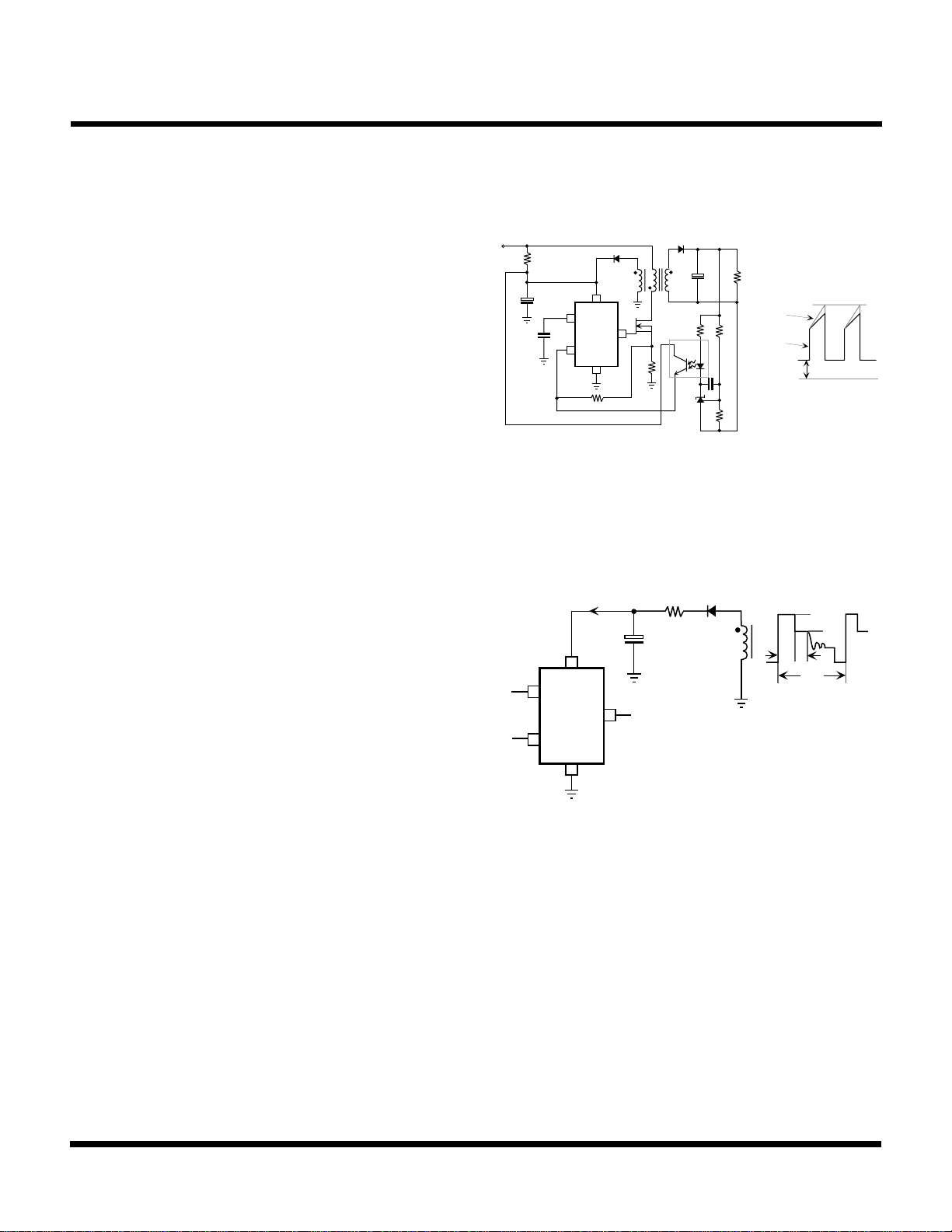
Figure 1 shows the typical application of the TK75003 in an
off-line flyback power supply (input full-wave bridge and
capacitor not shown). The IC starts when the voltage
across the capacitor C
V
of the IC. The starting resistor RST can be designed
IN(ON)
reaches the UVLO on Voltage
AUX
as follows:
R
ST(MAX)
= (V
IN(MIN)
- V
CC(ON,MAX)
- 2 V) / I
CC(START,MAX)
(1)
At 85 Vrms line voltage, and taking into account the
specified maximum values of the UVLO on voltage and the
start-up supply current I
CC(START)
, the maximum allowed
value of the starting resistor is:
R
= (85 2- 16 - 2 ) / 1.0 mA = 102.2 kΩ
ST(MAX)
(2)
considering the component tolerances, ripple, and other
second-order effects. The upper limit for V
AUX
is the
minimum voltage of the built-in clamp (16 V). The lower
limit for V
is the maximum UVLO off voltage (12.0 V). It
AUX
is prudent to choose the mean value of those two voltages
(i.e., 14.0 V), as V
AUX
.
COMPENSATING FOR LEAKAGE INDUCTANCE
The leakage inductance of the flyback transformer causes
a voltage overshoot at turn-off of the MOSFET. The
magnitude and duration of the overshoot depends on the
leakage inductance, the peak current at turn-offs, and the
voltage-clamping circuit employed to limit the overshoot.
The overshoot tends to increase the auxiliary voltage. The
simplest solution to reduce that increase is to add a
resistor R
in series with the rectifier diode D3. The
AUX
optimal value of the resistor can be calculated from the
subcircuit shown in Figure 2.
The average current flowing in R
I
drawn by the IC. The following equation can be written
AUX
is equal to the current
AUX
from the equality:
A practical choice for the starting resistor is RST = 100 kΩ.
The worst-case dissipation of the resistor appears at high
line and at the minimum VCC voltage. At 265 Vrms line
voltage and 9 V V
,
the dissipation is 2.2 W, so a 3 W
CC
resistor should be used. Note that 1.0 mA reflects the worst
case I
CC(START)
at the edge of UVLO release.
SELECTING THE TRANSFORMER TURNS RATIO
During steady-state operations, the auxiliary supply voltage
is generated by the auxiliary winding n3 and the rectifier
diode D3. In the flyback power supply, neglecting the effect
of the leakage inductance of the transformer, the number
of turns of the auxiliary winding can be calculated from the
following equation:
n3 = n2 [(V
+ VD3) / (V
AUX
OUT
+ VD2)]
(3)
where VD2 and VD3 are the forward voltage drops of the
output rectifier diode and the auxiliary rectifier diode. The
voltage V
should be selected such that it stays between
AUX
the specified worst-case upper and lower limits of the IC,
I
AUX
= (1 / R
AUX)
x ([(V1 - V
- V
) x (T1 / T)] + [(V2 - VD3 - V
D3
AUX
AUX)
x (T2 / T)])
(4)
The voltage V1 can be calculated as follows:
V1 = (V
+ VD2) x (n1 / n2) + [V
OUT
OVERSHOOT
x ( n3 / n1)]
(5)
where V
OVERSHOOT
is the additional voltage appearing
across the MOSFET due to the leakage inductance.
The voltage V2 can be calculated as follows:
V2 = (V
+ VD2) x ( n3 / n2)
OUT
(6)
Page 8 January 1999 TOKO, Inc.
Page 9
DESIGN CONSIDERATIONS (CONT.)
T1 is the time required for the leakage inductance of the
flyback transformer to completely discharge its stored
energy into the voltage clamp. T1 can be calculated as:
T1 = (IPK x L
(7)
where IPK is the peak current in the MOSFET at turn-off and
L
is the inductance of the flyback transformer measured
LEAK
at winding n1.
LEAK
) / V
OVERSHOOT
TK75003
D
V
IN
R
ST
V
AUX
C
AUX
C
T
D
3
n
3
V
CC
C
T
DRV
FB
GND
R
1
2
+
+
V
n
2
OC
R
S
TL431
OUT
STABILIZING
RAMP
SWITCH
CURRENT
SIGNAL
FEEDBACK
VOLTAGE
0.98 V
0
T2 is the conduction time of the output diode D2 and T is the
switching period.
From Equation 4 the resistance R
or the voltage V
AUX
AUX
can be calculated.
Example: calculate the value of R
with the following
AUX
typical values:
V
= 12 V VD2 = VD3 = 1 V IPK = 1 A
OUT
L
= 2 µH V
LEAK
I
= 18 mA T2 = 2 µs T = 5 µs
AUX
OVERSHOOT
= 20 V V
= 13.5 V
AUX
n1 = 31 n2 = 6 n3 = 7
Equations 5, 6 and 7 yield V1 = 19.7 V, V2 = 15.2 V, and
T1 = 100 ns. Substituting those values into Equation 4 and
solving for R
R
AUX
= 20.6 Ω
AUX
yields:
Rounding the result to the nearest 5% standard value
gives R
AUX
= 20 Ω.
(a)
(b)
FIGURE 1: TK75003 IN A FLYBACK POWER SUPPLY
(a) SCHEMATIC (b) VOLTAGE AT FEEDBACK PIN
I
V
AUX
AUX
C
AUX
V
CC
C
T
DRV
FB
GND
D
R
AUX
3
V
1
+
n
V
3
n3
_
V
T2T
1
T
FIGURE 2: SUBCIRCUIT FOR CALCULATING THE
VALUE OF R
AUX
January 1999 TOKO, Inc. Page 9
Page 10
TK75003
APPLICATION INFORMATION
SELF-BIASED POWER SUPPLY WITH CONSTANTFREQUENCY CURRENT-MODE CONTROL
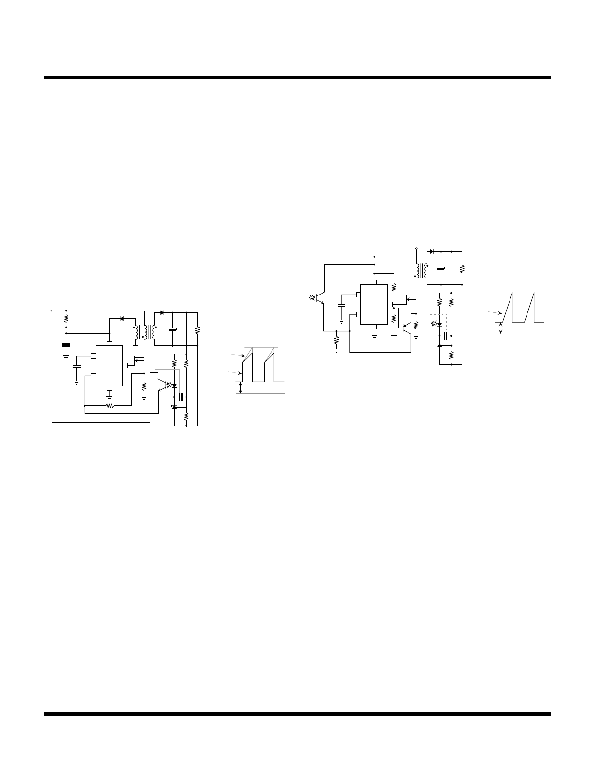
Figure 3(a) shows the TK75003 IC in the typical application:
a flyback converter with self-bias and constant-frequency
current- mode control. Figure 3(b) shows the feedback pin
voltage. In the converter, the voltage-error amplifier (a
TL431 shunt regulator IC) is located at the output side and
the error signal is transmitted to the input side through the
opto-coupler OC. Three signals are added together at the
feedback pin: 1) the feedback voltage that develops across
the resistor R1, 2) the switch current signal, and 3) the
stabilizing ramp. In each cycle, the MOSFET switch is
turned off when the sum of those three signals reaches
0.98 V.
D
V
IN
R
ST
V
AUX
C
AUX
C
T
D
3
n
3
V
CC
C
T
DRV
FB
GND
R
1
2
+
+
V
n
2
OC
R
S
TL431
OUT
STABILIZING
RAMP
SWITCH
CURRENT
SIGNAL
FEEDBACK
VOLTAGE
0.98 V
mode control, that resistor is connected to the currentsense resistor of the converter. In voltage-mode control,
that resistor is connected to ground.
In voltage-mode control, overload protection can be realized
by adding a simple circuit to the control IC, as shown in the
figure. The PNP transistor Q1, turns on and pulls up the
feedback pin when the switch current times the resistance
of the sense RS reaches the threshold set by the resistive
divider R2 and R3 and the base-emitter voltage of Q1.
V
V
AUX
OC
R
V
CC
C
T
DRV
FB
GND
1
IN
+
R
2
R
3
OC
R
S
Q
1
TL431
PWM
RAMP
FEEDBACK
VOLTAGE
(a)
0
0.98 V
0
(b)
(a)
(b)
FIGURE 3: TK75003 IN A SELF-BIASED FLYBACK
CONVERTER WITH CONSTANT-FREQUENCY
VOLTAGE-MODE CONTROL
(a) SCHEMATIC (b) VOLTAGE AT FEEDBACK PIN
POWER SUPPLY WITH CONSTANT-FREQUENCY
VOLTAGE-MODE CONTROL AND CYCLE-BY-CYCLE
CURRENT LIMIT
Voltage-mode control is free from some of the
disadvantages (e.g., subharmonic instability and noise
sensitivity) of current-mode control. It is very easy to
implement that control method with the TK75003 IC.
Figure 4(a) shows the IC in a voltage-mode-controlled
flyback converter. Figure 4(b) shows the feedback pin
voltage. The only circuit difference between current-mode
control and voltage-mode control is in the connection of
the resistor R1, that terminates the feedback pin. In current-
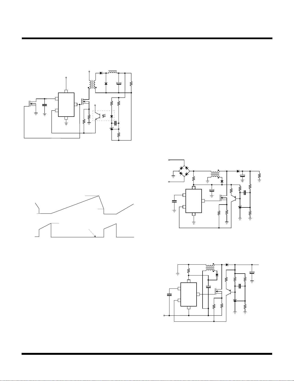
FIGURE 4: TK75003 IN A VOLTAGE-MODE-
CONTROLLED CONVERTER WITH ADDITIONAL
CYCLE-BY-CYCLE CURRENT LIMIT
(a) SCHEMATIC (b) VOLTAGE AT FEEDBACK PIN
POWER SUPPLY WITH CONSTANT OFF-TIME
CURRENT-MODE CONTROL
The advantages of constant off-time current-mode control
over constant-frequency current-mode control are: 1) there
is no need for a stabilizing ramp, 2) the converter is free
from subharmonic instability (i.e., there is no need for
slope compensation), and 3) the line voltage variation is
automatically canceled in buck-derived converters (e.g.,
the forward converter). Figure 5 shows the implementation
of that control method. As can be seen, a transistor Q
must be added to the controller. Figure 6 shows the timingpin and feedback pin voltages for the TK75003. The
transistor Q1 keeps the timing pin at ground potential
during the on-time of the switch. Timing begins when the
drive output returns to low and Q1 is turned off. The off-time
for typical charge and discharge currents and peak and
valley voltages is:
1
Page 10 January 1999 TOKO, Inc.
Page 11
APPLICATION INFORMATION (CONT.)
TK75003
t
= CT x 14 kΩ.
OFF
Q
1
V
IN
V
AUX
+
V
CC
C
T
C
T
DRV
FB
GND
V
AUX
OC
R
S
R
1
TL431
FIGURE 5: TK75003 IN A FORWARD CONVERTER
WITH CONSTANT OFF-TIME CURRENT-MODE
CONTROL
3.2 V
C
T
0
1.1 V
CT
TK75003 IN NON-ISOLATED APPLICATIONS
Although the IC was intended for off-line power-supply
V
OUT
applications with the voltage-error amplifier at the isolated
output, it is easy and economical to use the device in nonisolated applications, too. Figure 7 shows a low-cost boost
power factor corrector controlled by the TK75003. Power
factor correction is achieved by controlling the boost
converter with constant-frequency peak-current control
and exploiting the variation of the allowed peak-current
level caused by the variable duty ratio and the stabilizing
ramp. Figure 8 shows a buck-boost converter with negative
input voltage and positive output voltage, controlled by the
TK75003. In both cases, the voltage-error amplifier is a
TL431 shunt regulator, and a PNP transistor provides
interface between the TL431 and the control IC.
V
AC
IN
V
CC
C
T
DRV
FB
GND
TL431
OUT
+
0.98 V
FB
FEEDBACK VOLTAGE LEVEL
FB
FIGURE 7: TK75003 IN A LOW COST BOOST
POWER FACTOR CORRECTOR
V
(+)
FIGURE 6: TIMING PIN AND FEEDBACK PIN
OUT
VOLTAGES WITH CONSTANT OFF-TIME CURRENT-
MODE CONTROL
V
CC
C
T
DRV
FB
GND
V
(-)
IN
TL431
FIGURE 8: NON-ISOLATED NEGATIVE-TO-POSITIVE
CONVERTER
January 1999 TOKO, Inc. Page 11
Page 12

TK75003
APPLICATION INFORMATION (CONT.)
BOOST POWER FACTOR CORRECTOR APPLICATION
CIRCUIT
Figure 9 shows a universal-input, 100 W boost Power
factor corrector application circuit. The control technique is
called “current-clamped control.” Both the control technique
and the application circuit with waveforms are described in
the paper “Low-Cost Power Factor Correction/LineHarmonics Reduction with Current-Clamped Boost
Converter,” published in the conference proceedings of
Power Conversion Electronics ’95/Powersystems World™
’95. A copy of the paper can be obtained by contacting
Toko.
For designers who wish to explore other performance
optimizations of the current-clamped boost power factor
corrector, aside from the conference paper Toko offers a
Mathcad© file which can accurately display current
waveforms and predict power factor, harmonic distortion,
and individual harmonic currents. The Mathcad file and the
text which describes how to use it are available from the
Colorado Springs Toko IC Design Center.
The power factor corrector in Figure 9 has been optimized
for general wide-range-input use. In order to obtain the
same performance at power levels other than 100 W, the
control components do not need to change. The power
component values change as follows: C8 scales in
proportion to the power level, and L1 and R8 scales in
inverse proportion to the power level. Typically, although
not directly related to the line-current shaping capability of
the application circuit, C1 and C10 would scale in proportion
to the power level. All the components in the power stage
should have a current rating as needed to accommodate
the power level.
Below is a step-by-step design example, showing how to
determine the resistance of R7 terminating the feedback
pin and the resistance of the current-sense resistor R8, for
the boost corrector of Figure 9.
Assumptions:
Switching frequency: f = 100 kHz
Inductance of boost inductor: L1 = 2.5 mH
Maximum duty ratio of TK75005: D
MAX
= 0.88
Peak value of ramp current
flowing out of the FB pin: I
SC(PK)
= 200 µA
Threshold voltage of the
current-control detector: V
= 0.98 V
CCD
Calculations:
Peak value of minimum line voltage:
V
I(MIN)(PK)
= 2 x V
I(MIN)
= 120 V
PK
Switch duty ratio at peak of minimum line voltage:
D = 1 - V
I(MIN)(PK)
/ V
OUT
= 0.684
Peak-to-peak ripple current in inductor L1:
I = V
I(MIN)(PK)
x D / (f x L1) = 0.33 A
Input power at minimum line voltage:
PI = P
/ EFF = 107.5 W
OUT
Peak current in L1 (at peak of minimum line voltage):
I
=2 x PI / V
L1(PK)
I(MIN)(PK)
+ I / 2 = 1.95 A
Output power: P
Output voltage: V
Minimum line voltage: V
= 100 W
OUT
= 380 Vdc
OUT
= 85 Vrms
I(MIN)
Resistance of resistor R7 (Note 1):
R7 = D
MAX
x V
CCD
/ I
SC(PK)
= 4.312 kohms
Efficiency at 85 Vrms: EFF = 0.93
Page 12 January 1999 TOKO, Inc.
Page 13
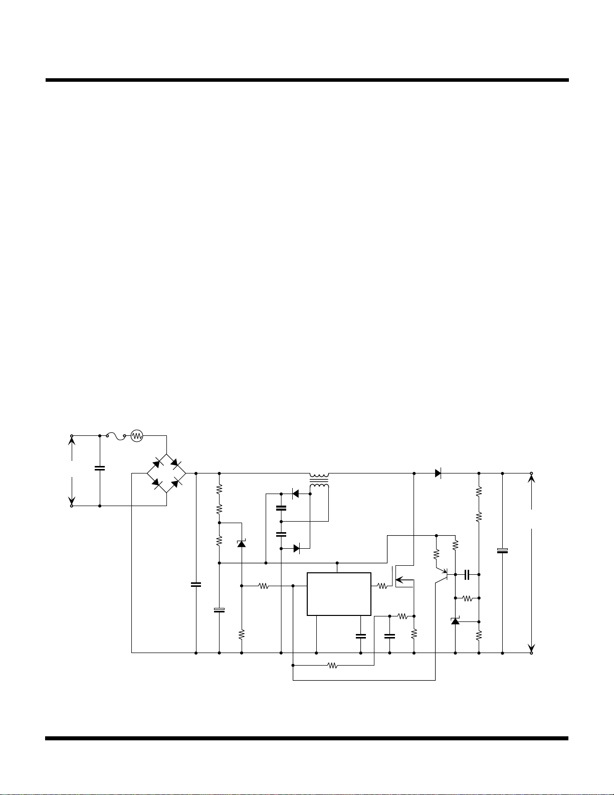
APPLICATION INFORMATION (CONT.)
Select for R7:
R7 = 4.3 kohms
Resistance of current-sense resistor R8 (Note 2):
TK75003
R8 = (V
CCD
- I
SC(PK)
x R7 x D) / I
= 0.201 ohms
L1(PK)
Select for R8:
R8 = 0.18 ohms
Note 1: This value of R7 ensures that the line current will be zero around
the zero-crossing of the line voltage, which is the required condition for
low-distortion line current.
Note 2: This value of R8 ensures that the sum of the voltage drop across
R8 (caused by the peak inductor current) and the voltage drop across R
(caused by the instantaneous value of the stabilizing current) is equal to
the threshold voltage of the current-control detector at the peak of the
line voltage.
F
85-265
VAC
1
2 A / 250 V
C
1
0.1 µF
TH
10 Ω
1
B
1
600 V, 1.5 A
R
24 k
0.5 W
C
1 nF
400 V
R
1a
24 k
0.5 W
1b
R
2
D
5.6 k
30 V
10
C
2
470 µF
R
3
5.6 k
4
150 k
1N4148
100 nF
100 nF
D2 IN4148
R
4
7
D
1
C
3
C
4
L
1
2.5 mH
t: 220
ETD-29 core
gap in center leg
t:9
V
CC
FB
GND C
U
1
TK75003
C
5
820 pF
5 %
R
7
4.3 k
DRV
T
D
3
HFA04TB60
+
R
11a
200 k
0.25 W
R
11b
200 k
0.25 W
R
10
1.2 k
R
Q
2907A
R
0.18
0.5 W
9
33 k
2
8
U
2
TL431
R
13
100 k
C
0.33 µF
R
12
2.43 k
Q
1
IRF840
R
5
10
R
6
51
C
6
10 nF
380 V DC
100 W
C
8
100 µF
400 V
7
-
FIGURE 9: BOOST POWER FACTOR CORRECTOR APPLICATION CIRCUIT
January 1999 TOKO, Inc. Page 13
Page 14
TK75003
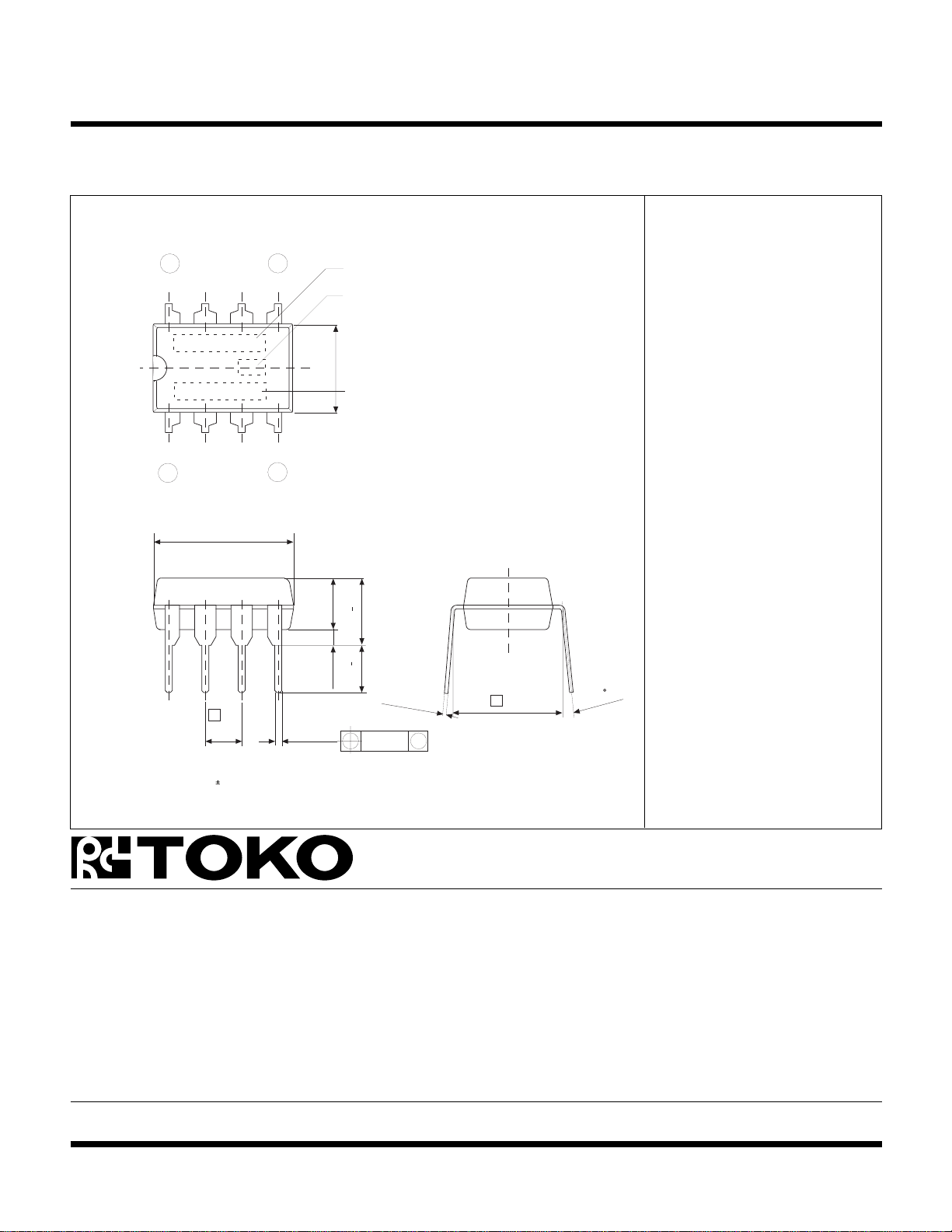
PACKAGE OUTLINE
DIP-8
Marking Information
8
1
9.5
e
2.54
5
Marking
Marking
TK75003 75003
Lot Number
6.4
Country of Origin
4
0.3
+
3.3
3.8
0.3
+
3.3
0.46
+ 0.15
- 0.05
0.5 min
0.25
0.25
+ 0.15
- 0.05
e1
7.62
M
0 ~15
Dimensions are shown in millimeters
Tolerance: x.x = 0.2 mm (unless otherwise specified)
Toko America, Inc. Headquarters
1250 Feehanville Drive, Mount Prospect, Illinois 60056
Tel: (847) 297-0070 Fax: (847) 699-7864
TOKO AMERICA REGIONAL OFFICES
Midwest Regional Office
Toko America, Inc.
1250 Feehanville Drive
Mount Prospect, IL 60056
Tel: (847) 297-0070
Fax: (847) 699-7864
Western Regional Office
Toko America, Inc.
2480 North First Street , Suite 260
San Jose, CA 95131
Tel: (408) 432-8281
Fax: (408) 943-9790
Eastern Regional Office
Toko America, Inc.
107 Mill Plain Road
Danbury, CT 06811
Tel: (203) 748-6871
Fax: (203) 797-1223
Semiconductor Technical Support
Toko Design Center
4755 Forge Road
Colorado Springs, CO 80907
Tel: (719) 528-2200
Fax: (719) 528-2375
Visit our Internet site at http://www.tokoam.com
The information furnished by TOKO, Inc. is believed to be accurate and reliable. However, TOKO reserves the right to make changes or improvements in the design, specification or manufacture of its
products without further notice. TOKO does not assume any liability arising from the application or use of any product or circuit described herein, nor for any infringements of patents or other rights of
third parties which may result from the use of its products. No license is granted by implication or otherwise under any patent or patent rights of TOKO, Inc.
Page 14 January 1999 TOKO, Inc.
© 1999 Toko, Inc.
All Rights Reserved
IC-121-TK75003
0798O0.0K
Printed in the USA
 Loading...