

Page 1

TK83361M
NARROW BAND FM IF IC
FEATURES
n Wide Operating Voltage Range 2.0 to 8.0V
n RF Input Frequency up to 220 MHz
n Low Supply Current (2.8mA, squelch off, 3.8mA,
squelch on)
n Low External Component Count
n Excellent Limiting Sensitivity (-3dB = 8dB
µµ
µ)
µµ
DESCRIPTION
The TK83361M is a narrow band FM IF IC designed for
cordless phones, radio transceivers, remote controls, wireless data transceivers, and other communication equipment.
It integrates the mixer, oscillator, limiting amplifier, FM
demodulator, filter amplifier and squelch circuit into a single
surface mount SOP-16 package. The low operating current combined with a minimum operating voltage of only 2
V makes this device ideal for battery powered devices.
The TK83361M offers improved performance over the
MC3361C. The operating frequency has been increased to
220MHz (vs. 60MHz) while reducing the supply current
from 5.2 mA to 3.8mA (squelch on). Offered in the SOP-16
surface mount package, the TK83361M is a drop-in replacement for the MC3361C.
APPLICATIONS
n Amateur Radio Transceivers
n Cordless Phones
n Remote Controls
n Wireless Data Transceivers
n Battery Powered Devices
TK83361M
1
OSC (B)
2
OSC (E)
3
MIXER OUT
4
VCC
5
IF INPUT
6
DECOUPLE
7
DECOUPLE
89
QUAD COIL
16
RF INPUT
15
GND
14
SCAN CONTROL
13
SCAN CONTROL
12
SQUELCH INPUT
FILTER AMP
11
OUTPUT
10
FILTER AMP
INPUT
AF OUTPUT
BLOCK DIAGRAM
ORDERING INFORMATION
TK83361M
Tape/Reel Code
TAPE/REEL CODE
TL: Tape Left
MIXER OUT
DECOUPLE
DECOUPLE
QUAD COIL
1
OSC (B)
OSC (E)
IF INPUT
OSC
2
3
SQUELCH
VCC
4
VCC
5
6
LIMIT
AMP
7
10pF
89
QUAL DET
MIXER
FILTER
AMP
GND
16
15
14
13
12
11
10
RF INPUT
GND
SCAN CONTROL
SCAN CONTROL
SQUELCH INPUT
FILTER AMP
OUTPUT
FILTER AMP
INPUT
AF OUTPUT
December 2000 TOKO, Inc. Page 1
Page 2

TK83361M
ABSOLUTE MAXIMUM RATINGS
Supply Voltage ........................................................ 10 V
Operating Voltage......................................... 2.0 to 8.0 V
Power Dissipation (Note 1) ................................ 600 mW
TK83361M ELECTRICAL CHARACTERISTICS
Test Conditions: V
LOBMYSRETEMARAPSNOITIDNOCTSETNIMPYTXAMSTINU
4.0 V, fRF = 10.7 MHz, VRF = +80dBµ, fm = 1kHz, f
CC =
unless otherwise specified.
Storage Temperature Range................... -55 to +150 °C
Operating Temperature Range.................. -30 to +70 °C
Input Frequency ............................................... 220 MHz
= ±3kHz, f
dev
= 10.245MHz, Ta = 25°C,
OSC
I
1CC
I
2CC
L
timi
V
O
Z
O
DHTnoitrotsiDcinomraHlatoTV
G
M
R
MI
G
f
f
CO
S
H
S
L
S
H
1tnerruCylppuSffohcleuqS,langiSoN8.25.3Am
2tnerruCylppuSnohcleuqS,langiSoN8.39.4Am
ytivitisneSgnitimiLBd3-)zHk1(.tpBd3-851µBd
egatloVtuptuOV
ecnadepmItuptuOV
FR
FR
FR
Bd08+= µ f,
Bd08+= µ f,
Bd08+= µ f,
ved
ved
ved
zHk3±=031071smrVm
zHk3±=054
zHk3±=68.05.2%
niaGnoisrevnoCrexiMdetanimret:3niP1282Bd
ecnadepmItupnIrexiMtnemerusaeMCD3.3kΩ
niaGreifilpmAretliFf
ni
tuptuOreifilpmAretliF
egatloVlanimreT
leveLhgiHlortnoCnacSVtupnIhcleuqS
leveLwoLlortnoCnacSVtupnIhcleuqS
leveLhgiHlortnoCnacSVtupnIhcleuqS
V,zHk01=
ni
Vm3.0=0405Bd
langiSoN5.07.09.0V
V0.0=0.39.3V
QS
V5.2=0.04.0V
QS
V5.2=0.39.3V
QS
Ω
S
L
H
SY
Note 1: Power dissipation must be decreased at a rate of 4.8 mW/°C for operation above 25°C.
leveLwoLlortnoCnacSVtupnIhcleuqS
V0.0=0.04.0V
QS
siseretsyHhcleuqS 54001Vm
Page 2 December 2000 TOKO, Inc.
Page 3

TEST CIRCUIT
(
)
V
O(DET)
, AMR, N, THD vs.
RF INPUT SIGNAL LEVEL
VIF, IF INPUT SIGNAL LEVEL (dBµ)
-20 ±0 +20 +40 +60 +80 +100 +120
V
O(DET)
, Output Level, AMR, AM
REJECTION AND N, NOISE (dBV)
-10
-20
-30
-40
-50
-60
-70
-80
Vcc=4.0V
fIF=455kHz
fm=1kHz, f
dev
=±3kHz
0.0
1.0
2.0
3.0
4.0
5.0
6.0
7.0
N
THD
AMR
(MOD.=30%)
V
O(DET)
THD, TOTAL HARMONIC
DISTORTION(%)
TK83361M
CF = BLFC455D (TOKO)
CFU455D2 (MURATA)
QUAD COIL = 7MCS-13546Z
9 - 1. Mixer + IF Section
V
O(DET
-10
-20
-30
-40
-50
RF INPUT SIGNAL LEVEL
10µF
0.1µF
QUAD
COIL
10.245MHz
33pF
+
120pF
VCC
0.1µF
0.1µF
20kΩ
1
MIXER
OSC
2
3
CF
SQUELCH
VCC
4
5
6
FILTER
LIMIT
AMP
AMP
7
10pF
89
QUAD DET
GND
0.01µF
16
50Ω
15
14
13
12
11
10
100kΩ
10kΩ
470kΩ
510Ω
8.2kΩ
1µF
+
1µF
+
0.01µF
VCC
TYPICAL PERFORMANCE CHARACTERISTICS
), AMR, N, THD vs.
7.0
Vcc=4.0V
fRF=10.7MHz
fm=1kHz, f
dev
f
=10.245MHz
OSC
AMR(mod=30%)
V
O(DET)
=±3kHz
THD, TOTAL HARMONIC
6.0
DISTORTION(%)
5.0
4.0
3.0
-60
), OUTPUT LEVEL, AMR, AM
-70
REJECTION AND N, NOISE (dBV)
O(DET
-80
V
-20 ±0 +20 +40 +60 +80 +100 +120
VRF, RF INPUT SIGNAL LEVEL (dBµ)
4.0
3.5
3.0
2.5
2.0
LEVEL (V)
1.5
1.0
0.5
SUPPLY VOLTAGE, OUTPUT
0.0
-0.5 0.0 0.5 1.0 1.5 2.0 2.5 3.0 3.5 4.0
December 2000 TOKO, Inc. Page 3
THD
TRANSIENT RESPONSE
fRF = 10.7MHz
τR, RISE TIME (msec)
fm = 1kHz
f
= ±3kHz
dev
f
= 10.245MHz
OSC
V
= ±0dBm
OSC
2.0
1.0
N
0.0
V
1kHz±3kHz
Non-mod
CC
20dB NQS vs. RF INPUT
FREQUENCY
0
20dB NQS = 17.5dBµ
-20
fRF = 10.7MHz
f
= 10.245MHz
OSC
-40
-60
0
20dB NQS = 18.0dBµ
RELATIVE 20dB NQ
SENSITIVITY(dB)
-20
fRF = 58MHz
f
= 58.545MHz
OSC
-40
-60
-20 -15 -10 -5 ±0 +5 +10 +15 +20
fRF±∆fRF, RF INPUT
FREQUENCY
kHz
Page 4

TK83361M
SINAD, GM S/N vs. LOCAL OSC
INPUT SIGNAL LEVEL
V
OSC
, LOCAL OSC INPUT SIGNAL
LEVEL (dBµ)
-70 -60 -50 -40 -30 -20 -10 0 10 20
SINAD, 12dB SINAD SENSITIVITY
(dBµ) S/N, signal to noise ratio (dB)
60
50
40
30
20
0
10
35
30
25
20
15
10
0
G
M
fRF = 10.7MHz
21MHz
58MHz
83MHz
S/N
SINAD
G
M
, MIXER CONVERSION
GAIN(dB)
µ
TYPICAL PERFORMANCE CHARACTERISTICS (CONT.)
9 - 2. Mixer Section
32
30
28
(dB)
26
VCC = 4.0V
fRF VARIABLE
VRF = +60dBµ
24
, MIXER CONVERSION GAIN
G
fOM = 455kHz
V
M
22
1M 10M 100M 1G
fRF, RF INPUT FREQUENCY (Hz)
THE 3rd ORDER INTERCEPT
140
120
1st ORDER DESIRED
fRF = 10.7MHz
100
MIXER INPUT FREQUENCY
RESPONSE
= ±0dBm
OSC
POINT
IIP3 = 107dBµ
MIXER OUTPUT FREQUENCY
0
RESPONSE
-2
-4
-6
-8
-10
-12
VCC = 4.0V
LEVEL (dB)
fRF = 10.7MHz
-14
, RELATIVE MIXER OUTPUT
OMR
V
VRF = +60dBµ
-16
f
VARIABLE
OSC
V
= ±0dBm
OSC
-18
-20
100k 1M 10M
fOM, MIXER OUTPUT FREQUENCY
(Hz)
80
(dBµ)
60
, MIXER OUTPUT LEVEL
3rd ORDER INTERMOD
40
f
RF1
OM
f
V
20
RF2
20 40 60 80 100 120
VRF, RF INPUT SIGNAL LEVEL
9 - 3. IF Section
OUTPUT LEVEL, TOTAL HARMONIC
DISTORTION vs. IF INPUT FREQUENCY
-10
-20
-30
-40
, OUTPUT LEVEL(dBV)
-50
O(DET)
V
-60
-40 -30 -20 -10 ±0 +10 +20 +30 +40
455±∆fIF, IF INPUT FREQUENCY (kHz)
Page 4 December 2000 TOKO, Inc.
= 10.7125MHz
= 10.725MHz
V
O(DET)
(dB
)
VCC = 4.0V
VIF = ±80dBµ
fm = 1kHz
f
=±3kHz
dev
THD
10.0
8.0
DISTORTION(%)
6.0
4.0
2.0
0.0
THD, TOTAL HARMONIC
OUTPUT DC VOLTAGE vs.
IF INPUT FREQUENCY
4.0
3.5
3.0
VCC = 4.0V
VIF = +80dBµ
2.5
2.0
V
1.5
1.0
, OUTPUT DC VOLTAGE (V)
.5
O(DC)
V
0
CC
QUAD
R
D
COIL
8
-80 -60 -40 -20 ±0 +20 +40 +60 +80
455±∆fIF, IF INPUT FREQUENCY (kHz)
RD = 5kΩ
RD = 10kΩ
RD = 20kΩ
Page 5

TYPICAL PERFORMANCE CHARACTERISTICS (CONT.)
(
)
THD
TOTAL
HARMONIC
OUTPUT LEVEL, TOTAL HARMONIC
DISTORTION vs. IF DEVIATION
600
VCC =4.0V
500
fIF = 455kHz
VIF = +80dBµ
fm = 1kHz
400
300
200
V
, OUTPUT LEVEL(mVrms)
O(DET)
100
O(DET)
V
0
0 1 2 3 4 5 6 7 8 9 10
f
dev.
9 - 4. Filter Amplifer Section
GAIN vs. INPUT FREQUENCY
70
60
50
40
30
20
10
, FILTER AMPLIFIER GAIN (dB)
f
G
0
1k 10k 100k 1M
9 - 5. Squelch Section
SCAN CONTROL vs. SQUELCH
4.0
SC
3.5
FREQUENCY
, IF DEVIATION FREQUENCY
kHz
11
R
f
10
R
1
fin, FILTER AMPLIFIER INPUT
FREQUENCY (Hz)
INPUT VOLT AGE
TK83361M
OUTPUT LEVEL vs. IF MODULATION
THD
6.0
5.0
4.0
3.0
2.0
1.0
THD, T O TAL HARMONIC
DISTORTION(%)
RD =
20kΩ
±0
10kΩ
-10
5kΩ
-20
, RELATIVE OUTPUT
LEVEL (dB)
-30
VCC =4.0V
fIF = 455kHz
-40
VIF = +80dBµ
f
dev
Pin 9: open
O(DET)R
V
0.0
100 1k 10k 100k 1M
fm, IF MODULATION FREQUENCY (HZ)
10
VCC = 4.0V
Vin = 0.3mV
R1 = 510Ω
Rf = 470kΩ
1
1µF
+
1µF
+
100m
, OUTPUT LEVEL(Vrms)
out
V
10m
0.1 1 10 100
SC
FREQUENCY
V
CC
QUAD
COIL
8
= ±3kHz
R
D
INPUT LEVEL RESPONSE
THD
V
VCC = 4.0V
Fin = 10kHz
R1 = 510Ω
Rf = 470kΩ
Vin, INPUT LEVEL(mVrms)
OUT
100
10.0
1.0
0.1
DISTORTION(%)
,
3.0
2.5
2.0
1.5
1.0
SC, SC, SCAN CONTROL(V)
0
.60 .65 .70 .75 .80
VSQ, SQUELCH INPUT VOLTAGE(V)
VCC = 4.0V
December 2000 TOKO, Inc. Page 5
Page 6
TK83361M
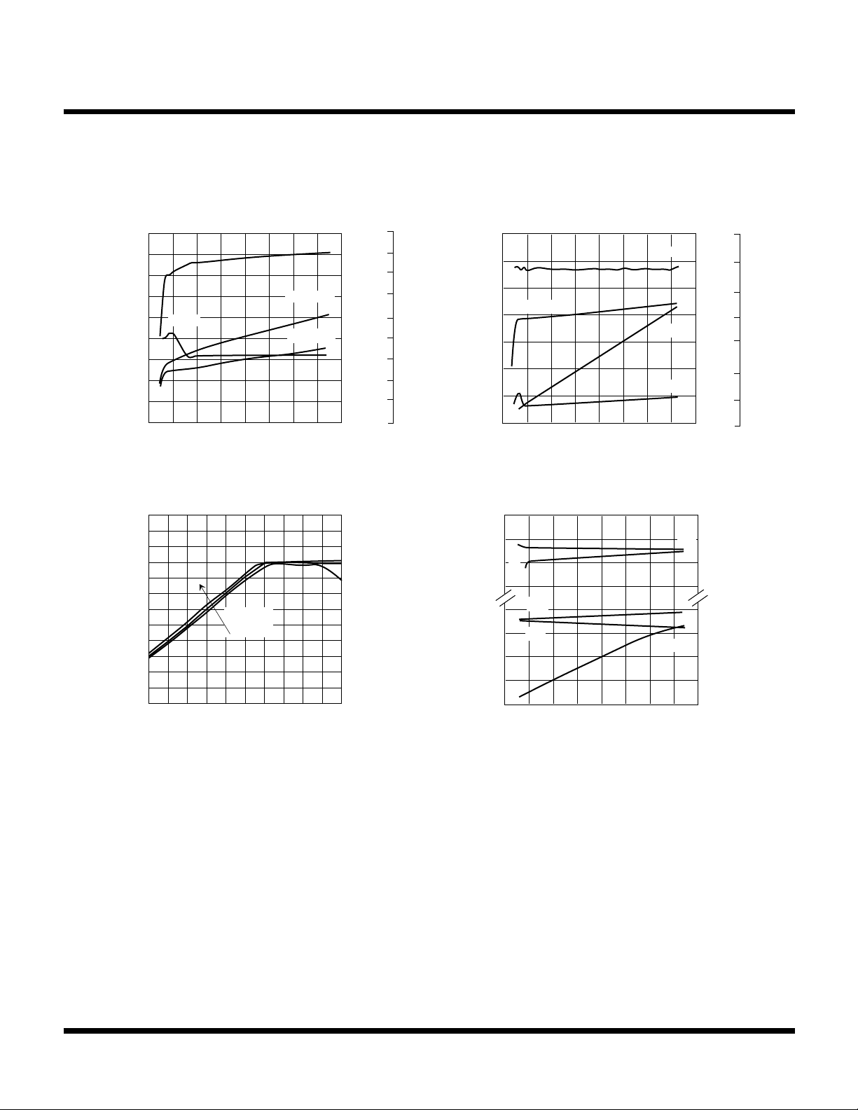
TYPICAL PERFORMANCE CHARACTERISTICS (CONT.)
9 - 6. Versus Supply Voltage Characteristics
SUPPLY CURRENT, 12dB SINAD
SENSITIVITY, MIXER CONVERSION
GAIN vs. SUPPLY VOLTAGE
I
: sq off
CC2
SINAD
I
: sq on
CC1
1 2 3 4 5 6 7 8 9
VCC, SUPPLY VOLTAGE(V)
MIXER OUTPUT LEVEL vs. SUPPLY
VOLT AGE
80
60
VCC = 8.5V
4.0V
2.0V
40
20
20 40 60 80 100 120
VRF, RF INPUT SIGNAL
LEVEL(dBµ)
G
M
, MIXER OUTPUT LEVEL(dBµ)
V
, SUPPLY CURRENT(mA)
CC
I
140
120
100
OM
9.0
8.0
7.0
6.0
5.0
4.0
3.0
2.0
1.0
0.0
18
16
14
12
10
OUTPUT LEVEL, TOTAL HARMONIC
DISTORTION, SIGNAL TO NOISE
SINAD, 12dB SINAD SENSITIVITY(dBµ)
36
32
G
M
, MIXER CONVERSION GAIN(dB)
28
24
20
8
6
4
2
0
16
12
8
4
0
RATIO, OUTPUT DC VOLTAGE vs.
0
SUPPLY VOL TAGE
-5
-10
V
O(DET)
-15
-20
), OUTPUT LEVEL(dBV)
-25
-30
O(DET
V
-35
1 2 3 4 5 6 7 8 9
S/N
V
O(DC)
THD
7
6
THD(%),V
5
4
O(DC)
3
(V)
2
1
0
60
50
40
30
20
10
0
70
S/N, SIGNAL TO NOISE RATIO (dB)
VCC, SUPPLY VOLTAGE(V)
FILT. AMP. GAIN, FILT. AMP. OUTPUT
DC VOLT AGE, THRESHOLD V OLT AGE,
HYSTERESIS vs. SUPPLY VOLTAGE
70
60
G
50
, FILTER
f
G
, THRESH-
TL
, V
TH
V
f
40
AMP. GAIN(dB)
0.8
0.6
V
TH
V
TL
0.4
0.2
OLD VOLTAGE(V)
0.0
1 2 3 4 5 6 7 8 9
HYS
1.0
f
DC VOL TAGE
OC
f
OC
0.8
, OUTPUT
0.6
0.4
HYSTERESIS(mV)
HYS, SQUELCH
120
90
60
30
0
VCC, SUPPLY VOLTAGE(V)
Page 6 December 2000 TOKO, Inc.
Page 7
TK83361M
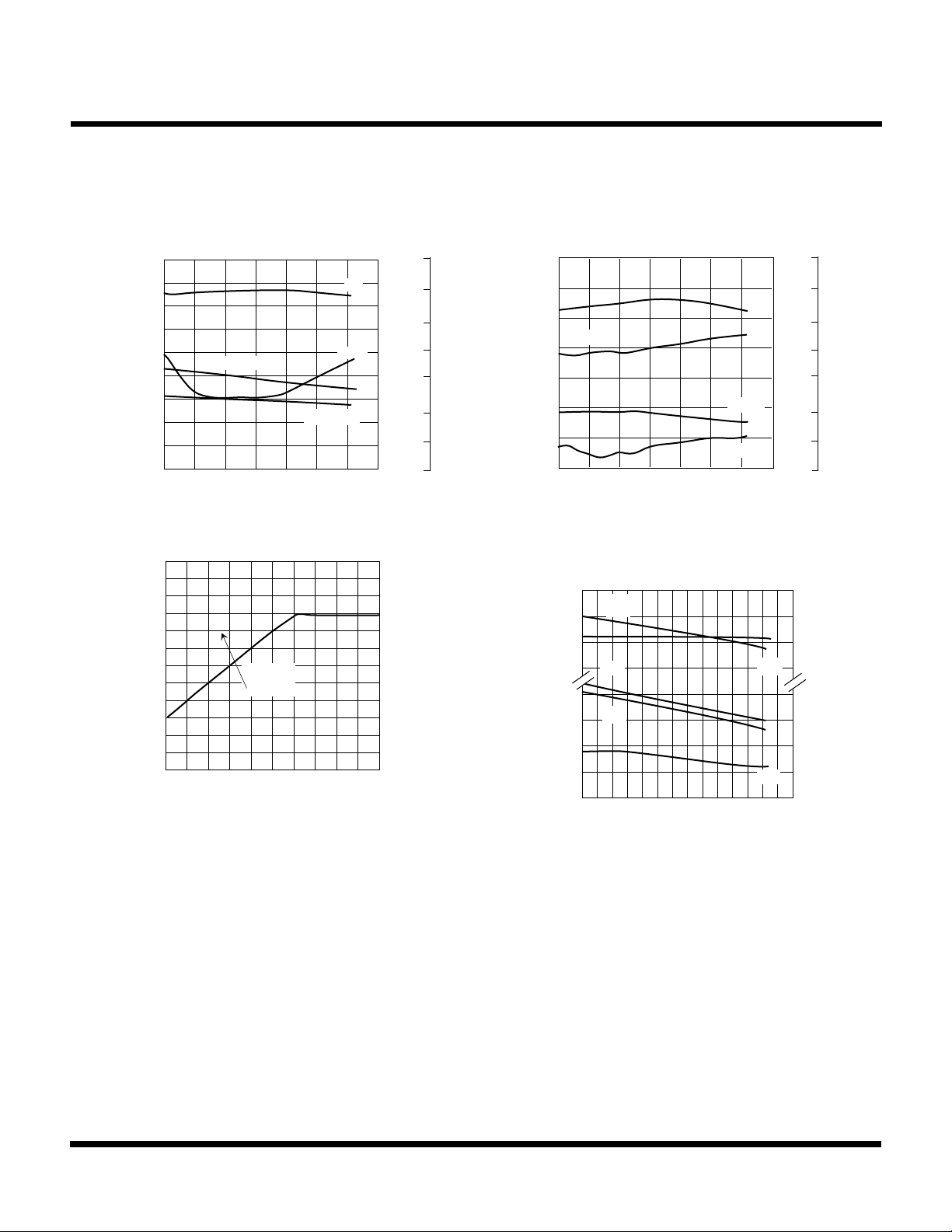
TYPICAL PERFORMANCE CHARACTERISTICS (CONT.)
9 - 7. Versus Ambient Temperature Characteristics
SUPPLY CURRENT, 12dB SINAD
SENSITIVITY, MIXER CONVERSION
GAIN vs. AMBIENT TEMPERATURE
9
8
7
6
5
4
I
CC2
: sq off
3
I
, SUPPLY CURRENT(mA)
I
CC
2
1
CC1
0
-40 -20 0 20 40 60 80 100
Ta, AMBIENT TEMPERATURE (°C)
MIXER OUTPUT LEVEL vs.
AMBIENT TEMPERA TURE
140
120
100
, MIXER OUTPUT LEVEL(dBµ)
OM
V
80
60
40
20
Ta = +25°C
+85°C
-40°C
20 40 60 80 100 120
VRF, RF INPUT SIGNAL
LEVEL(dBµ)
SINAD
: sq on
G
M
18
16
14
12
10
SINAD, 12dB SINAD SENSITIVITY(dBµ)
16
8
6
4
2
0
36
32
28
24
20
12
8
4
0
OUTPUT LEVEL, TOTAL HARMONIC
DISTORTION, SIGNAL TO NOISE
RATIO, OUTPUT DC VOLTAGE vs.
G
M
, MIXER CONVERSION GAIN(dB)
-5
-10
-15
AMBIENT TEMPERA TURE
0
V
O(DET)
S/N
7
6
THD(%),V
5
4
60
50
40
70
S/N, SIGNAL TO NOISE RATIO (dB)
O(DC)
30
O(DC)
THD
3
(V)
20
2
10
1
0
0
-20
, OUTPUT LEVEL(dBV)
-25
-30
O(DET)
V
-35
-40 -20 0 20 40 60 80 100
V
Ta, AMBIENT TEMPERATURE(°C)
FILT. AMP. GAIN, FILT. AMP. OUT-
PUT DC VOLTAGE,
THRESHOLD VOLTAGE,
,
, V
V
TL
TH
HYSTERESIS vs. AMBIENT TEMP.
70
60
G
f
50
40
0.8
0.6
V
TH
V
TL
GAIN(dB)
, FILTER AMP.
f
G
0.4
0.2
VOLTAGE(V)
THRESHOLD
0.0
-40 -20 0 20 40 60 80 100
f
OC
HYS
1.0
0.8
0.6
0.5
120
90
60
30
0
f
OC
VOLTAGE(V)
, OUTPUT DC
HYSTERESIS(mV)
HYS, SQUELCH
Ta, AMBIENT TEMPERATURE(°C)
December 2000 TOKO, Inc. Page 7
Page 8
TK83361M
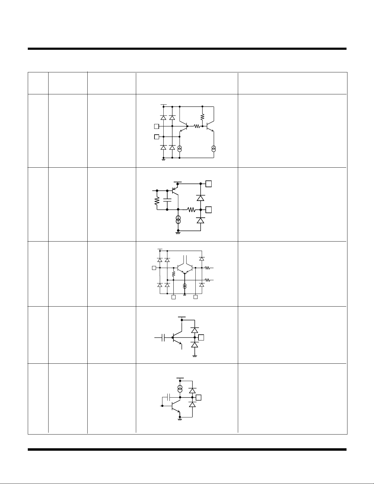
PIN FUNCTION DESCRIPTION
PIN
1
SYMBOL
OSC(B) The base of the Colpitts oscillator.
TERMINAL
VOLTAGE (V)
INTERNAL EQUIVALENT CIRCUIT
V
CC
DESCRIPTION
The Colpitts oscillator is composed of
Pin 1 and Pin 2.
1
2 OSC(E)
2
The emitter of the Colpitts oscillator.
Using an external OSC source, local
level must be injected into Pin 1, and
Pin 2 must be opened.
3 Output of the Mixer.
MIXER OUT
4
V
CC
5
IF INPUT Input to the IF limiter amplifier.
V
CC
V
CC
4
3
Supply Voltage.
This pin is terminated by internal
1.8kW resistor.
IF Decoupling.
6
DECOUPLE
5
1.8k
51.8K
50K
7
8
9
DECOUPLE
QUAD COIL
AF OUTPUT
10p
10p
6
7
V
CC
8
V
CC
9
IF Decoupling
Phase Shifter.
Recovered Audio Output
Page 8 December 2000 TOKO, Inc.
Page 9
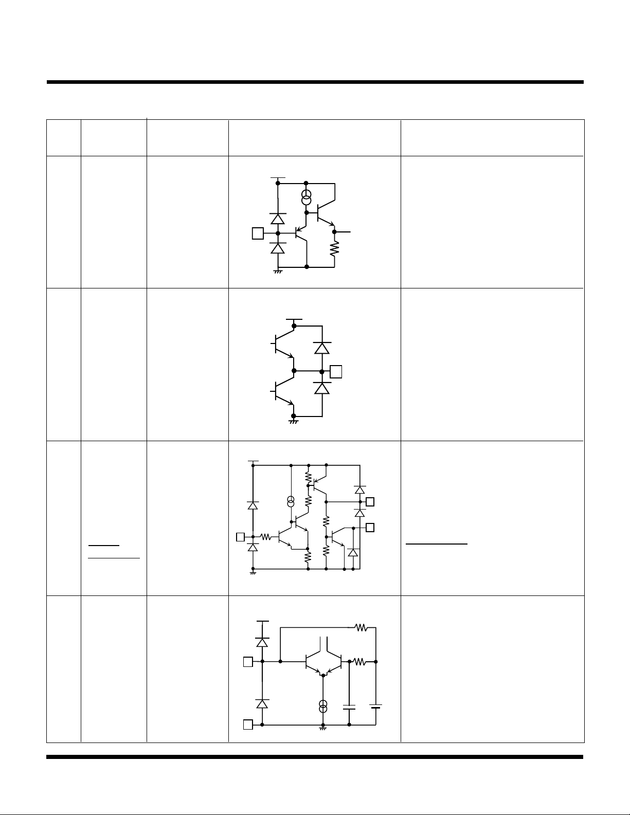
PIN FUNCTION DESCRIPTION (CONT.)
TK83361M
PIN
10
11
SYMBOL
FILTER
AMPLIFIER
INPUT
FILTER
AMPLIFIER
OUTPUT
TERMINAL
VOLTAGE (V)
INTERNAL EQUIVALENT CIRCUIT
V
CC
10
V
CC
11
DESCRIPTION
Filter Amplifier Input.
Filter Amplifier Output.
12
13
14
15
SQUELCH
INPUT
SCAN
V
CC
13
Squelch Input.
Scan Control.
CONTROL
14
Scan Control.
SCAN
12
20k
CONTROL
GND
V
CC
3.3K
Ground
RF INPUT16 Mixer Input.
16
15
3.3K
December 2000 TOKO, Inc. Page 9
Page 10
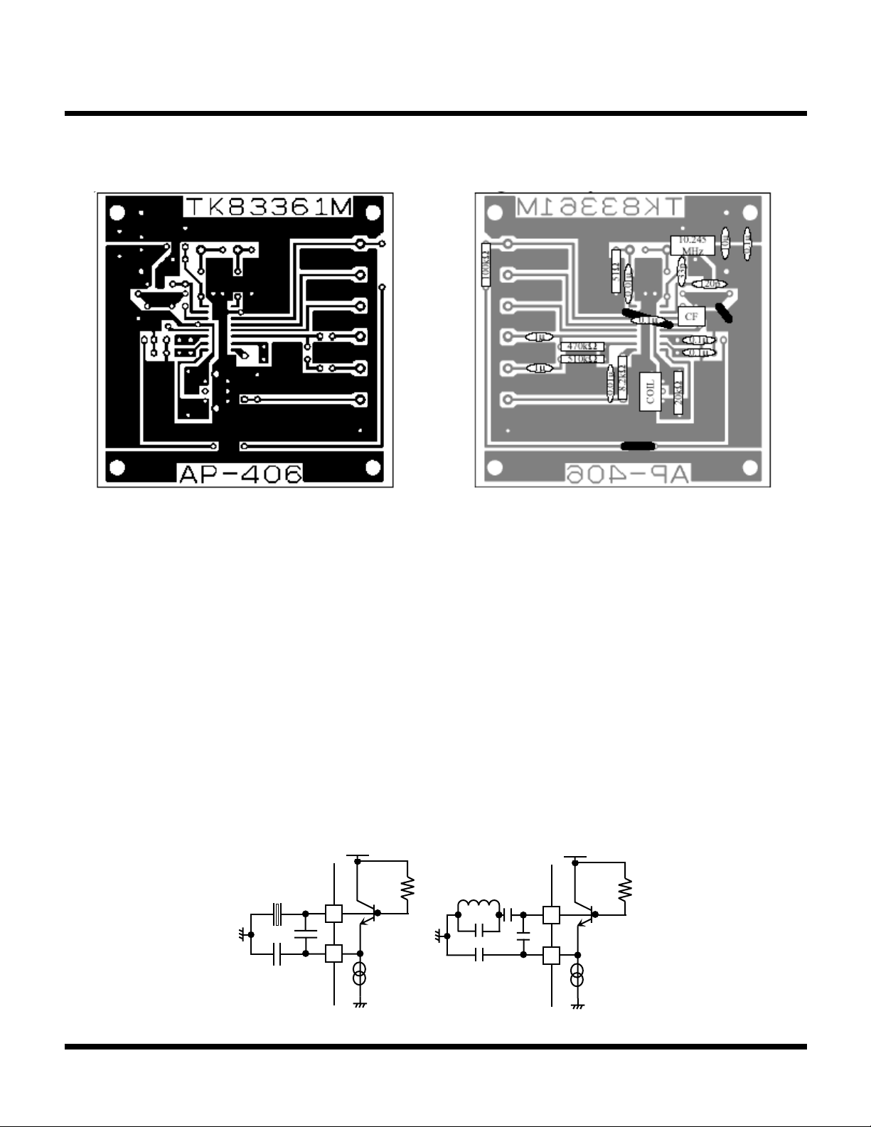
TK83361M
TEST BOARD
Figure 1: Solder Side View (Circuit Side View) Figure 2: Component Placement View
NOTES:
1. Above test board is laid out for the TEST CIRCUIT (page 3).
2. Scale 1:1 (60mmx60mm)
3. 10.245MHz Fundamental mode crystal, about 30pF load.
4. 455kHz CF, TOKO Type BLFC455D or MURATA Type
CFU455D2 or equivalent.
5. COIL, TOKO Type 7MCS-13546Z or 7MC-8128Z or
equivalent.
APPLICATIONS INFORMATION
12-1. Mixer Section
The mixer consists of a Gilbert cell and a local oscillator. The mixer conversion gain, when Pin 4 is terminated, is 28dB.
The RF input is unbalanced.
12-1-1. A Local OSC
The oscillator included is a general Colpitts type OSC. The drive current of OSC is 200µA. Examples of components are
shown in Fig. 3. The examples are explained in the next paragraph.
Figure 3: Oscillator Components
i) Under Crystal Control
V
CC
1
ii) Parallel LC Components
V
CC
1
2
Page 10 December 2000 TOKO, Inc.
2
Page 11
APPLICATIONS INFORMATION (CONT.)
C
(1) Using an External Oscillator Source
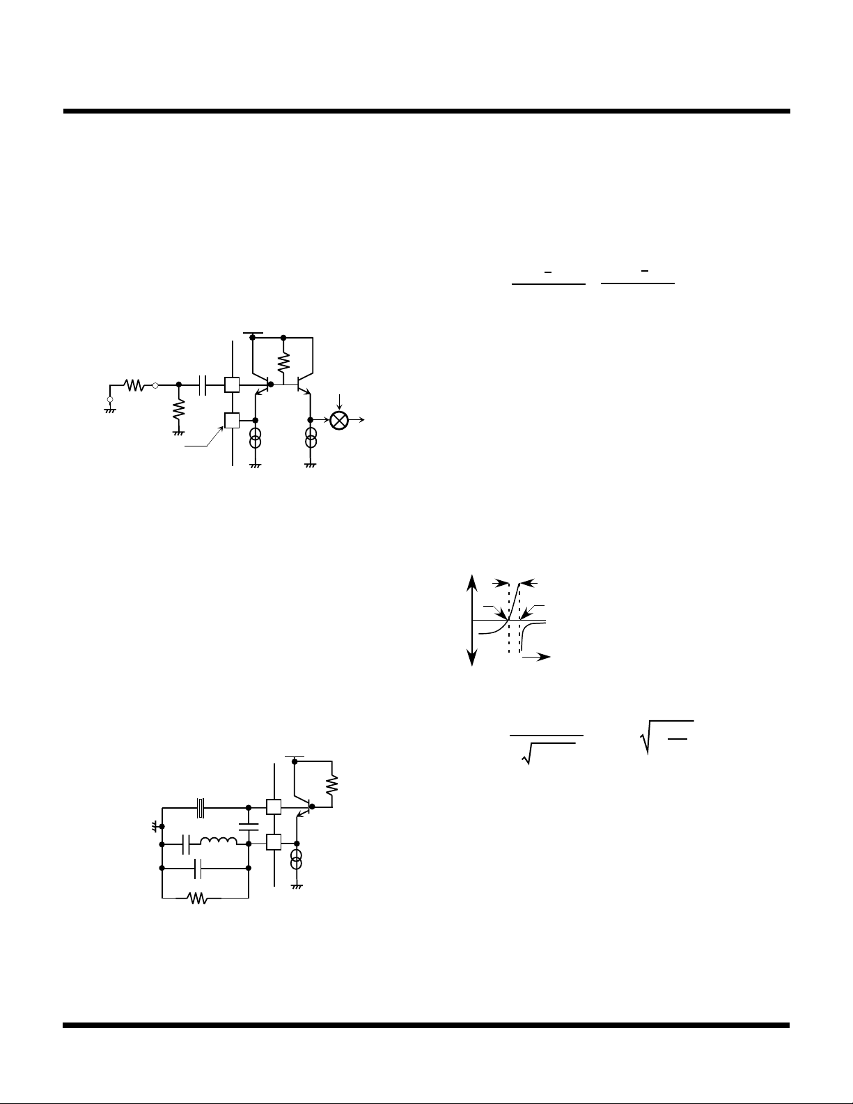
The circuit composition using an external OSC source is
shown in Fig. 4. When using an external OSC source
instead of the internal OSC, the local level must be injected
into Pin 1 by capacitor coupling.
In this case, Pin 2 must be open.
The local OSC operates as an emitter follower for a multiplier by opening Pin 2 and injecting into Pin 1.
Figure 4: External Injection
V
CC
TK83361M
tor. It is easy to increase the drive current by connecting
resistor R
current, it makes gm increase to increase the drive current
by connecting external resistor Re. In that case, the amount
of drive current increase, Ie, is shown in Eq.(1).
between Pin 2 and GND. Being short of drive
e
Ie =
V
CC
V
Re
BE
V
=
CC
Re
0.7
(1)
50Ω
~
0.01µ
50Ω
open
1
2
RF
IF
(2) For 3rd Overtone mode
In general, a crystal oscillator can oscillate in the fundamental mode and overtone mode. For example, it is easy for a
30MHz-overtone crystal to oscillate at 10MHz, fundamental
mode. The reason is because the impedance of the fundamental mode is the same as the impedance of the overtone.
Therefore, it is necessary for the circuit to select the
overtone frequency by using a tuning coil.
How to oscillate a general 3rd overtone oscillator is explained. In the case of an overtone mode of 30MHz and
higher, using a crystal oscillator, we recommend the circuit
in Fig. 5 to suppress the fundamental mode oscillation.
Figure 5: Overtone Mode Circuit
V
CC
In order to oscillate at the 3
rd
overtone frequency, the values
of C2, C3 and L (Fig.5) are selected. Fig.6 shows a 2-port
impedance response of the C2~C3~L loop network.
Regarding the condition of oscillation, the impedance characteristic is capacitive at the vacinity of the overtone frequency. It is reactive at the vicinity of the fundamental
frequency.
The condition of oscillation is as follows:
f
is between fa and fb,
OSC
3 x f
is fb and higher. Please see Fig.6
OSC
Figure 6: 2-port
Impedance Response of Resonance Network
+j
f
OSC
f
a
f
b
Where:
fa: series resonant freq.
fb: parallel resonant freq.
Reactance
-j
3 X f
OS
f
: fundamental mode freq.
OSC
3 x f
OSC
:
3rd order overtone freq.
Equations of 3rd order overtone oscillation are shown below.
fa =
1
2π LxC
,
fb =f
2
C
2
1+
a
C
3
(2)
X’tal
1
C
L
2
C
3
C
1
2
The series value of the equivalent capacitance at the 3
order overtone freq. of this network, which is decided in the
above -mentioned, and the capacitance of C1 must be equal
to load capacitance CL.
Being short of negative resistance of the circuit, increase
the transistor’s bias current by decreasing Re. It is able to
R
e
decide the OSC level for minute adjusting Re. Please refer
the most suitable OSC level range to 12dB SINAD sensitivity versus local OSC input signal level in TYPICAL PER-
The following explains how to decide the circuit constants of
the overtone-crystal-oscillation fundamental circuit.
As the operating frequency increases the oscillation amplitude decreases because of a shortage of gm of the oscilla-
FORMANCE CHARACTERISTICS. The saturating range
is the most suitable OSC level range. It is comparatively
easy to decide the circuit constant by examining it with a
network analyzer.
December 2000 TOKO, Inc. Page 11
rd
Page 12
TK83361M
APPLICATIONS INFORMATION (CONT.)
12-2. IF Section
The IF section includes a 6 stage differential amplifier. The
fixed internal input matching resistor is 1.8kΩ. The total gain
of the limiting amplifier section is approximately 77dB.
The decoupling capacitors of Pin 6~7 must be connected as
near as possible to the GND pin of the IC . And, make the
impedance of the connecting-to-GND line to be as small as
possible. If the impedance is not small enough, the sensitivities may worsen.
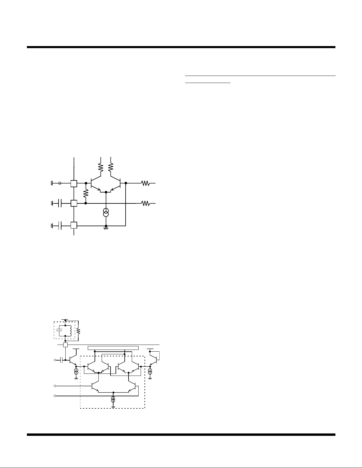
Figure 7: IF Limiter Amplifier Input Block
5
1.8k
6
7
50K
51.8K
12-3. FM Demodulator
A quadrature FM demodulator using a Gilbert cell is included.
12-3-1. Internal Equivalent Circuit
The internal equivalent circuit is shown in Fig. 8.
Figure 8: Internal Equivalent Circuit of Demodulator
V
CC
QUAD
COIL
from IF LIM AMP
10pF
R
D
8
V
CC
Q
1
Active Load
V
CC
Q
2
Note at this point to add the bias voltage at Pin 8 from
external source.
The signal from the phase shifter is put into the multiplier cell
through the emitter follower of transistor Q1. Pin 8 is singleconnected with the base terminal. And, it is necessary for
Pin 8 to add the same voltage, as the base terminal of Q2 of
the opposite side of Q1 through the multiplier is connected
with the supply voltage.
If the base voltages differ between transistors Q1 and Q2, it
alters the DC zero point or worsens the distortion of the
demodulation output.
12-3-2. Phase Shifter
The IF signal from the limiter amplifier is provided with 90°
phase shift and drives the quadrature detector.
The parallel RCL resonance circuit is capable of using the
internal 10pF phase shift capacitor.
12-3-3. Audio Output
After quadrature detection, the audio signal is pulled out
through Pin 9.
The required signal is pulled out through the LPF.
12-3-4. For Stable Operation
To prevent worsening the distortion, observe the following
notes:
(1) Demodulated Output Voltage
Too large of a demodulated output voltage will worsen the
distortion due to the dynamic range of the demodulator.
(2) The Signal Level in Phase Shifter (Pin 8)
If the phase shifter signal level is too small, the noise level
grows worse. This will cause the distortion to grow worse.
(3) Band Width of Phase Shifter (Pin 8)
If the bandwidth of the phase shifter is narrower than IF
bandwidth, including the demodulated element, the distortion will grow worse.
12-4. Filter Amplifier Section
An inverting op amp has an output at Pin 11 and the inverting
input at Pin 10. The op amp, which has a wide stable
operating temperature range, may be used as an active
noise filter.
Multiplier
Cell
12-4-1. Active BPF Application
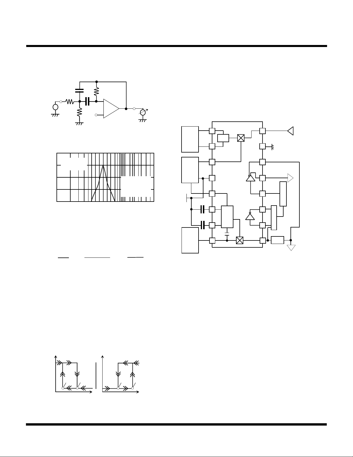
An active BPF application is shown in Fig. 9, and its
Response is shown in Fig. 10.
Page 12 December 2000 TOKO, Inc.
Page 13
APPLICATIONS INFORMATION (CONT.)
R
H
LPF
NETWORK
RECTIFIER
XTAL
NETWORK
1
2
3
4
5
6
7
89
10
11
12
13
14
15
16
RF
INPUT
SCAN CONTROL
to PLL
VCC
OSC
MIXER
LIMIT
AMP
10pF
QUAD DET
VCC
SQUELCH
GND
FILTER
AMP
NARROW
BAND
BPF
PHASE
SHIFTER
0.1µF
0.1µF
AF
OUTPUT
MUTE
Figure 9. Active BPF
TK83361M
VTH indicates the Hi threshold voltage, VTL indicates the Lo
threshold voltage in Fig. 11.
C
R
R
1
V
~
IN
C
R
2
3
-
+
V
OUT
Figure 10. Frequency Response
20
VCC = 4.0V
15
Vin = 50mV
10
GAIN (dB)
5
0
1k 10k 100k
fin, FILTER AMPLIFIER INPUT FREQUENCY (Hz)
R1 = 18kΩ
R2 = 750Ω
R3 = 390kΩ
C = 0.001µF
Eq. (3) is formularized, where G0 is the gain at center
frequency f0, and 3dB bandwidth Q=f0/BW.
R1R
3
4Q2R1-R
3
2G
3
0
R1 = , R2 = , R3 = (3)
Q
πf0C
12-6. Application Example
Figure 12: Application Example Block Digram
12-5. Squelch Section
The output, which is controlled in accordance with the noise
level from the rectifier, is injected into the squelch input pin.
There is about 45mV of hysteresis at the Squelch Input to
prevent jitter.
VSQ(V)
V
TL
V
T
Figure 11. Squelch Output versus Squelch Input
December 2000 TOKO, Inc. Page 13
i) Pin 13 Output
Scan Control(V)
V
TL
VSQ(V)
V
ii) Pin 14 Output
Scan Control(V)
TH
12-7. Attentions to Layout Design
As this product is considered for stable operation, the mixer
block and the other block that includes IF stage, OP amp
and squelch are independent from each other. However in
order to realize stable operation, please pay attention to the
following, because of high frequency operation.
(1) Bypass Capacitor
A bypass capacitor must be connected with minimum
distance between the VCC pin and the GND pin.
(2) VCC/GND Pattern
In order to make low impedance VCC/GND lines, please
keep the pattern as wide as possible.
(3) Pattern near Demodulator
Pattern layout around the phase shifter for demodulator:
please keep as short as possible.
Page 14

TK83361M
NOTES
WARNING - Life support applications policy.
TOKO, Inc. products shall not be used within any life support systems without the specific written consent of TOKO, Inc.
A life support system is a product or system intended to support or sustain life which, if it fails, can be reasonably expected
to result in a significant personal injury or death.
The contents of this application as of December 2000. The contents of this datasheet are subject to change without notice
or stop manufacture.
The circuits shown in this specification are intended to explain typical applications of the products concerned. Accordingly,
TOKO, Inc. is not responsible for any circuit problems, or for any infringement of third party patents or any other intellectual
property rights that may arise from the use of these circuits. Moreover, this specification dose not signify that TOKO, Inc.
agrees implicitly or explicitly to license any patent rights or other intellectual property rights which it holds.
No Ozone Depleting Substances (ODS) were used in the manufacture of these parts.
Examples of characteristics given here are typical for each product and being technical data, these do not constitute a
guarantee of characteristics or conditions of use.
Page 14 December 2000 TOKO, Inc.
Page 15
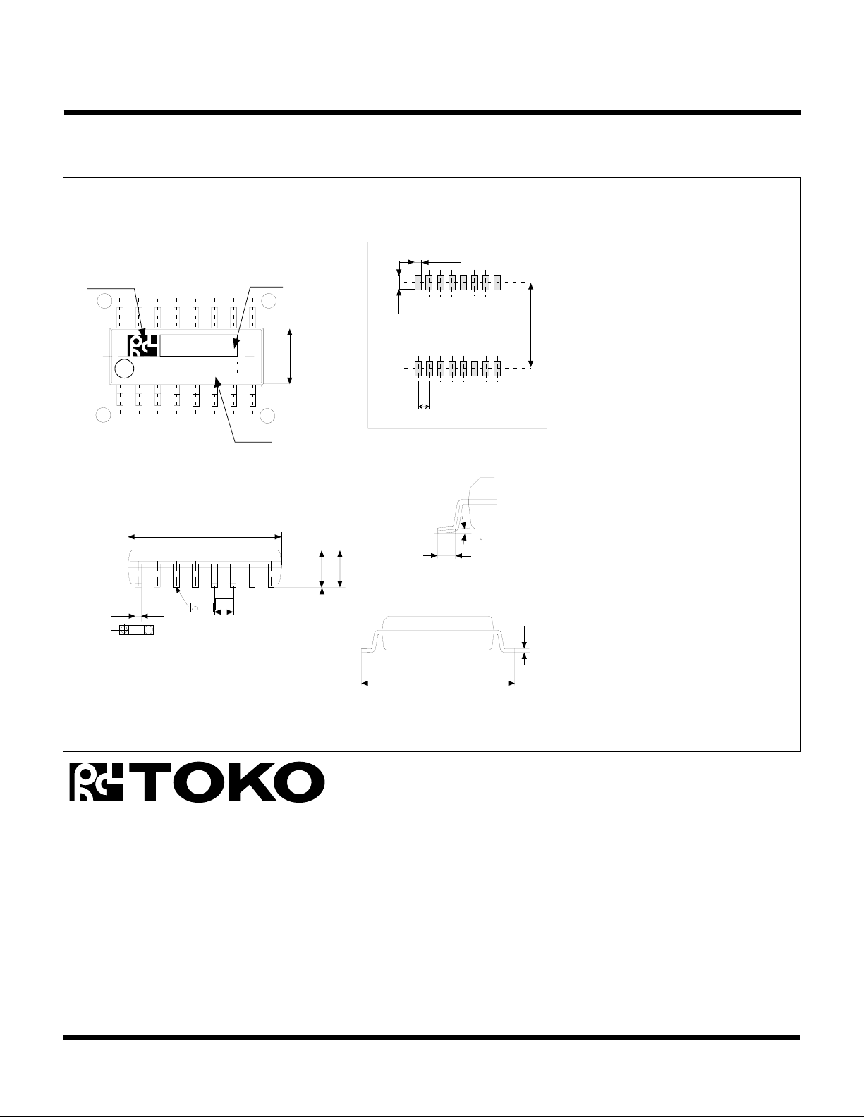
PACKAGE OUTLINE
TK83361M
SOP-16
TOKO Mark
16
1
+0.15
0.4
-0.05
0.12
Marking Information
0.76
Mark
9
±0.2
YYY
Lot No.
±0.2
9.9
1.27
0.1
M
3.9
8
±0.2
1.45
1.75 max
0 ~ 0.25
1.27
1.27
Recommended Mount Pad
±0.2
0.5
0 ~ 10
+0.15
0.2
5.4
-0.05
Marking
TK83361M 83361
Dimensions are shown in millimeters
Tolerance: x.x = ± 0.2 mm (unless otherwise specified)
6.0
±0.3
Toko America, Inc. Headquarters
1250 Feehanville Drive, Mount Prospect, Illinois 60056
Tel: (847) 297-0070 Fax: (847) 699-7864
TOKO AMERICA REGIONAL OFFICES
Midwest Regional Office
Toko America, Inc.
1250 Feehanville Drive
Mount Prospect, IL 60056
Tel: (847) 297-0070
Fax: (847) 699-7864
Western Regional Office
Toko America, Inc.
2480 North First Street , Suite 260
San Jose, CA 95131
Tel: (408) 432-8281
Fax: (408) 943-9790
Semiconductor Technical Support
Toko Design Center
4755 Forge Road
Colorado Springs, CO 80907
Tel: (719) 528-2200
Fax: (719) 528-2375
Visit our Internet site at http://www.tokoam.com
The information furnished by TOKO, Inc. is believed to be accurate and reliable. However, TOKO reserves the right to make changes or improvements in the design, specification or manufacture of
its products without further notice. TOKO does not assume any liability arising from the application or use of any product or circuit described herein, nor for any infringements of patents or other rights
of third parties which may result from the use of its products. No license is granted by implication or otherwise under any patent or patent rights of TOKO, Inc.
December 2000 TOKO, Inc. Page 15
All Rights Reserved
IC-231-TK11031
0798O0.0K
Printed in the USA© 2000 Toko, Inc.
 Loading...