

Page 1
November 1992 Order Number: 271070-006
M82380
HIGH PERFORMANCE 32-BIT DMA CONTROLLER WITH
INTEGRATED SYSTEM SUPPORT PERIPHERALS
Y
High Performance 32-Bit DMA
Controller
Ð 40 Mbytes/sec Maximum Data
Transfer Rate at 20 MHz
Ð 8 Independently Programmable
Channels
Y
20-Source Interrupt Controller
Ð Individually Programmable Interrupt
Vectors
Ð 15 External, 5 Internal Interrupts
Ð M8259A Superset
Y
Four 16-Bit Programmable Interval
Timers
Ð M82C54 Compatible
Y
Programmable Wait State Generator
Ð 0 to 15 Wait States Pipelined
Ð 1 to 16 Wait States Non-Pipelined
Y
DRAM Refresh Controller
Y
i386TMProcessor Shutdown Detect and
Reset Control
Ð Software/Hardware Reset
Y
High Speed CHMOS III Technology
Y
132-Pin PGA Package and 164-Pin Quad
Flat Pack
(See Packaging Specification OrderÝ231369)
Y
Optimized for use with the i386
TM
Microprocessor
Ð Resides on Local Bus for Maximum
Bus Bandwidth
Y
Available in Three Product Grades:
Ð MIL-STD-883,
b
55§Ctoa125§C(TC)
Ð Military Temperature Only,
b
55§Ctoa125§C(TC)
Ð Extended Temperature,
b
40§Ctoa110§C(TC)
The M82380 is a multi-function support peripheral that integrates system functions necessary in an i386
processor environment. It has eight channels of high performance 32-bit DMA with the most efficient transfer
rates possible on the i386 microprocessor bus. System support peripherals integrated into the M82380 provide
Interrupt Control, Timers, Wait State generation, DRAM Refresh Control, and System Reset logic.
The M82380’s DMA Controller can transfer data between devices of different data path widths using a single
channel. Each DMA channel operates independently in any of several modes. Each channel has a temporary
data storage register for handling non-aligned data without the need for external alignment logic.
271070–1
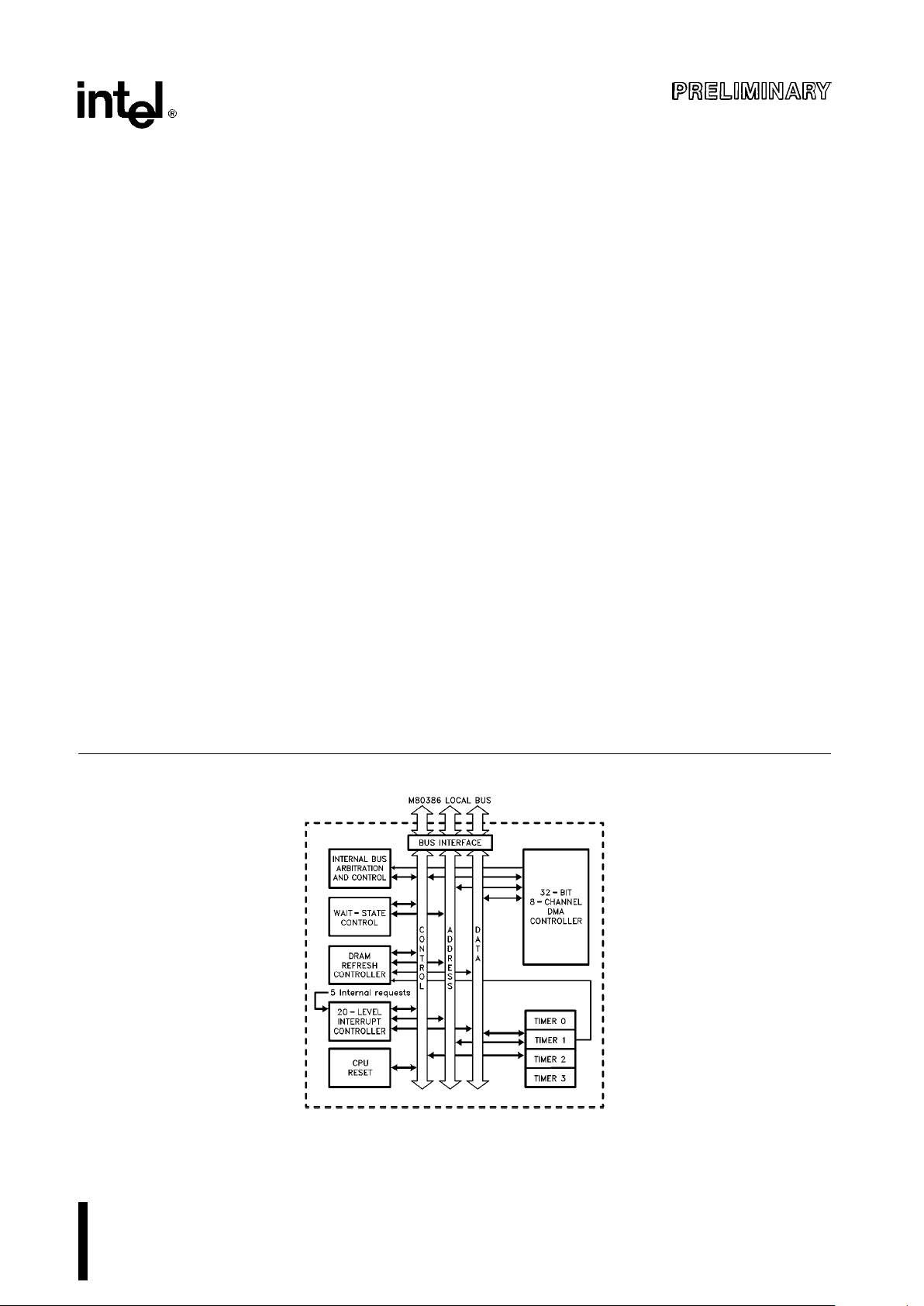
M82380 Internal Block Diagram
Page 2

M82380
M82380
HIGH PERFORMANCE 32-BIT DMA CONTROLLER
WITH INTEGRATED SYSTEM SUPPORT PERIPHERALS
CONTENTS PAGE
1.0 FUNCTIONAL OVERVIEW
ААААААААААААААААААААААААААААААААААААААААААААААААААААААААААААААА 6
1.1 M82380 Architecture ААААААААААААААААААААААААААААААААААААААААААААААААААААААААААААААААААА 6
1.1.1 DMA Controller ААААААААААААААААААААААААААААААААААААААААААААААААААААААААААААААААААА 7
1.1.2 Programmable Interval Timers ААААААААААААААААААААААААААААААААААААААААААААААААААААА 8
1.1.3 Interrupt Controller АААААААААААААААААААААААААААААААААААААААААААААААААААААААААААААААА 9
1.1.4 Wait State Generator ААААААААААААААААААААААААААААААААААААААААААААААААААААААААААААА 10
1.1.5 DRAM Refresh Controller АААААААААААААААААААААААААААААААААААААААААААААААААААААААА 10
1.1.6 CPU Reset Function ААААААААААААААААААААААААААААААААААААААААААААААААААААААААААААА 11
1.1.7 Register Map Relocation ААААААААААААААААААААААААААААААААААААААААААААААААААААААААА 11
1.2 Host Interface АААААААААААААААААААААААААААААААААААААААААААААААААААААААААААААААААААААААА 11
2.0 i386TMPROCESSOR HOST INTERFACE ААААААААААААААААААААААААААААААААААААААААААААААА 12
2.1 Master and Slave Modes АААААААААААААААААААААААААААААААААААААААААААААААААААААААААААААА 13
2.2 M80386 Interface Signals ААААААААААААААААААААААААААААААААААААААААААААААААААААААААААААА 13
2.2.1 Clock (CLK2) АААААААААААААААААААААААААААААААААААААААААААААААААААААААААААААААААААА 13
2.2.2 Data Bus (D0– D31) АААААААААААААААААААААААААААААААААААААААААААААААААААААААААААААА 13
2.2.3 Address Bus (A31– A2) ААААААААААААААААААААААААААААААААААААААААААААААААААААААААААА 14
2.2.4 Byte Enable (BE3– BE0) АААААААААААААААААААААААААААААААААААААААААААААААААААААААААА 14
2.2.5 Bus Cycle Definition Signals (D/C, W/R, M/IO) ААААААААААААААААААААААААААААААААААА 15
2.2.6 Address Status (ADS) АААААААААААААААААААААААААААААААААААААААААААААААААААААААААААА 15
2.2.7 Transfer Acknowledge (READY) ААААААААААААААААААААААААААААААААААААААААААААААААА 15
2.2.8 Next Address Request (NA) АААААААААААААААААААААААААААААААААААААААААААААААААААААА 15
2.2.9 Reset (RESET, CPURST) АААААААААААААААААААААААААААААААААААААААААААААААААААААААА 15
2.2.10 Interrupt Out (INT) АААААААААААААААААААААААААААААААААААААААААААААААААААААААААААААА 17
2.3 M82380 Bus Timing ААААААААААААААААААААААААААААААААААААААААААААААААААААААААААААААААААА 17
2.3.1 Address Pipelining ААААААААААААААААААААААААААААААААААААААААААААААААААААААААААААААА 17
2.3.2 Master Mode Bus Timing ААААААААААААААААААААААААААААААААААААААААААААААААААААААААА 17
2.3.3 Slave Mode Bus Timing АААААААААААААААААААААААААААААААААААААААААААААААААААААААААА 20
3.0 DMA CONTROLLER АААААААААААААААААААААААААААААААААААААААААААААААААААААААААААААААААААА 21
3.1 Functional Description АААААААААААААААААААААААААААААААААААААААААААААААААААААААААААААААА 22
3.2 Interface Signals АААААААААААААААААААААААААААААААААААААААААААААААААААААААААААААААААААААА 23
3.2.1 DREQn and EDACK (0–2) ААААААААААААААААААААААААААААААААААААААААААААААААААААААА 24
3.2.2 HOLD and HLDA ААААААААААААААААААААААААААААААААААААААААААААААААААААААААААААААААА 24
3.2.3 EOP ААААААААААААААААААААААААААААААААААААААААААААААААААААААААААААААААААААААААААААА 24
3.3 Modes of Operation ААААААААААААААААААААААААААААААААААААААААААААААААААААААААААААААААААА 24
3.3.1 Target/Requester Definition АААААААААААААААААААААААААААААААААААААААААААААААААААААА 25
3.3.2 Buffer Transfer Processes АААААААААААААААААААААААААААААААААААААААААААААААААААААААА 25
3.3.3 Data Transfer Modes ААААААААААААААААААААААААААААААААААААААААААААААААААААААААААААА 26
3.3.4 Channel Priority Arbitration ААААААААААААААААААААААААААААААААААААААААААААААААААААААА 30
3.3.5 Combining Priority Modes АААААААААААААААААААААААААААААААААААААААААААААААААААААААА 32
3.3.6 Bus Operation ААААААААААААААААААААААААААААААААААААААААААААААААААААААААААААААААААА 33
3.4 Bus Arbitration and Handshaking АААААААААААААААААААААААААААААААААААААААААААААААААААААА 34
3.4.1 Synchronous and Asynchronous Sampling of DREQn and EOP ААААААААААААААААААА 37
3.4.2 Arbitration of Cascaded Master Requests ААААААААААААААААААААААААААААААААААААААААА 39
3.4.3 Arbitration of Refresh Requests АААААААААААААААААААААААААААААААААААААААААААААААААА 41
2
Page 3

M82380
CONTENTS PAGE
3.0 DMA CONTROLLER (Continued)
3.5 DMA Controller Register Overview
АААААААААААААААААААААААААААААААААААААААААААААААААААА 41
3.5.1 Control/Status Registers ААААААААААААААААААААААААААААААААААААААААААААААААААААААААА 41
3.5.2 Channel Registers ААААААААААААААААААААААААААААААААААААААААААААААААААААААААААААААА 42
3.5.3 Temporary Registers ААААААААААААААААААААААААААААААААААААААААААААААААААААААААААААА 43
3.6 DMA Controller Programming ААААААААААААААААААААААААААААААААААААААААААААААААААААААААА 44
3.6.1 Buffer Processes ААААААААААААААААААААААААААААААААААААААААААААААААААААААААААААААААА 44
3.6.2 Data Transfer Modes ААААААААААААААААААААААААААААААААААААААААААААААААААААААААААААА 45
3.6.3 Cascaded Bus Masters ААААААААААААААААААААААААААААААААААААААААААААААААААААААААААА 45
3.6.4 Software Commands ААААААААААААААААААААААААААААААААААААААААААААААААААААААААААААА 45
3.7 Register Definitions ААААААААААААААААААААААААААААААААААААААААААААААААААААААААААААААААААА 46
4.0 PROGRAMMABLE INTERRUPT CONTROLLER АААААААААААААААААААААААААААААААААААААААА 53
4.1 Functional Description АААААААААААААААААААААААААААААААААААААААААААААААААААААААААААААААА 53
4.1.1 Internal Block Diagram ААААААААААААААААААААААААААААААААААААААААААААААААААААААААААА 53
4.1.2 Interrupt Controller Banks АААААААААААААААААААААААААААААААААААААААААААААААААААААААА 54
4.2 Interface Signals АААААААААААААААААААААААААААААААААААААААААААААААААААААААААААААААААААААА 55
4.2.1 Interrupt Inputs ААААААААААААААААААААААААААААААААААААААААААААААААААААААААААААААААААА 55
4.2.2 Interrupt Output (INT) АААААААААААААААААААААААААААААААААААААААААААААААААААААААААААА 56
4.3 Bus Functional Description АААААААААААААААААААААААААААААААААААААААААААААААААААААААААААА 56
4.4 Mode of Operation АААААААААААААААААААААААААААААААААААААААААААААААААААААААААААААААААААА 57
4.4.1 End-Of-Interrupt ААААААААААААААААААААААААААААААААААААААААААААААААААААААААААААААААА 57
4.4.2 Interrupt Priorities АААААААААААААААААААААААААААААААААААААААААААААААААААААААААААААААА 58
4.4.3 Interrupt Masking АААААААААААААААААААААААААААААААААААААААААААААААААААААААААААААААА 61
4.4.4 Edge Or Level Interrupt Triggering АААААААААААААААААААААААААААААААААААААААААААААААА 61
4.4.5 Interrupt Cascading АААААААААААААААААААААААААААААААААААААААААААААААААААААААААААААА 61
4.4.6 Reading Interrupt Status ААААААААААААААААААААААААААААААААААААААААААААААААААААААААА 62
4.5 Register Set Overview АААААААААААААААААААААААААААААААААААААААААААААААААААААААААААААААА 62
4.5.1 Initialization Command Words (ICW) АААААААААААААААААААААААААААААААААААААААААААААА 64
4.5.2 Operation Control Words (OCW) ААААААААААААААААААААААААААААААААААААААААААААААААА 64
4.5.3 Poll/Interrupt Request/In-Service Status Register АААААААААААААААААААААААААААААААА 65
4.5.4 Interrupt Mask Register (IMR) АААААААААААААААААААААААААААААААААААААААААААААААААААА 65
4.5.5 Vector Register (VR) ААААААААААААААААААААААААААААААААААААААААААААААААААААААААААААА 65
4.6 Programming ААААААААААААААААААААААААААААААААААААААААААААААААААААААААААААААААААААААААА 65
4.6.1 Initialization (ICW) АААААААААААААААААААААААААААААААААААААААААААААААААААААААААААААААА 65
4.6.2 Vector Registers (VR) АААААААААААААААААААААААААААААААААААААААААААААААААААААААААААА 66
4.6.3 Operation Control Words (OCW) ААААААААААААААААААААААААААААААААААААААААААААААААА 66
4.7 Register Bit Definition ААААААААААААААААААААААААААААААААААААААААААААААААААААААААААААААААА 67
4.8 Register Operational Summary АААААААААААААААААААААААААААААААААААААААААААААААААААААААА 70
3
Page 4

M82380
CONTENTS PAGE
5.0 PROGRAMMABLE INTERVAL TIMER
АААААААААААААААААААААААААААААААААААААААААААААААААА 71
5.1 Functional Description АААААААААААААААААААААААААААААААААААААААААААААААААААААААААААААААА 71
5.1.1 Internal Architecture ААААААААААААААААААААААААААААААААААААААААААААААААААААААААААААА 72
5.2 Interface Signals АААААААААААААААААААААААААААААААААААААААААААААААААААААААААААААААААААААА 73
5.2.1 CLKIN ААААААААААААААААААААААААААААААААААААААААААААААААААААААААААААААААААААААААААА 73
5.2.2 TOUT1, TOUT2, TOUT3 ААААААААААААААААААААААААААААААААААААААААААААААААААААААААА 73
5.2.3 GATE АААААААААААААААААААААААААААААААААААААААААААААААААААААААААААААААААААААААААААА 73
5.3 Modes of Operation ААААААААААААААААААААААААААААААААААААААААААААААААААААААААААААААААААА 74
5.3.1 Mode 0ÐInterrupt on Terminal Count АААААААААААААААААААААААААААААААААААААААААААА 74
5.3.2 Mode 1ÐGate Retriggerable One-Shot ААААААААААААААААААААААААААААААААААААААААААА 74
5.3.3 Mode 2ÐRate Generator АААААААААААААААААААААААААААААААААААААААААААААААААААААААА 76
5.3.4 Mode 3ÐSquare Wave Generator АААААААААААААААААААААААААААААААААААААААААААААААА 77
5.3.5 Mode 4ÐInitial Count Triggered Strobe ААААААААААААААААААААААААААААААААААААААААААА 79
5.3.6 Mode 5ÐGate Retriggerable Strobe АААААААААААААААААААААААААААААААААААААААААААААА 80
5.3.7 Operation Common to All Modes ААААААААААААААААААААААААААААААААААААААААААААААААА 81
5.4 Register Set Overview АААААААААААААААААААААААААААААААААААААААААААААААААААААААААААААААА 81
5.4.1 Counter 0, 1, 2, 3 Registers ААААААААААААААААААААААААААААААААААААААААААААААААААААААА 82
5.4.2 Control Word RegisterI&II АААААААААААААААААААААААААААААААААААААААААААААААААААААА 82
5.5 Programming ААААААААААААААААААААААААААААААААААААААААААААААААААААААААААААААААААААААААА 82
5.5.1 Initialization АААААААААААААААААААААААААААААААААААААААААААААААААААААААААААААААААААААА 82
5.5.2 Read Operation АААААААААААААААААААААААААААААААААААААААААААААААААААААААААААААААААА 82
5.6 Register Bit Definitions АААААААААААААААААААААААААААААААААААААААААААААААААААААААААААААААА 84
6.0 WAIT STATE GENERATOR ААААААААААААААААААААААААААААААААААААААААААААААААААААААААААААА 86
6.1 Functional Description АААААААААААААААААААААААААААААААААААААААААААААААААААААААААААААААА 86
6.2 Interface Signals АААААААААААААААААААААААААААААААААААААААААААААААААААААААААААААААААААААА 87
6.2.1 READY АААААААААААААААААААААААААААААААААААААААААААААААААААААААААААААААААААААААААА 87
6.2.2 READYO АААААААААААААААААААААААААААААААААААААААААААААААААААААААААААААААААААААААА 87
6.2.3 WSC(0 –1) ААААААААААААААААААААААААААААААААААААААААААААААААААААААААААААААААААААААА 87
6.3 Bus Function ААААААААААААААААААААААААААААААААААААААААААААААААААААААААААААААААААААААААА 88
6.3.1 Wait States in Non-Pipelined Cycle ААААААААААААААААААААААААААААААААААААААААААААААА 88
6.3.2 Wait States in Pipelined Cycle АААААААААААААААААААААААААААААААААААААААААААААААААААА 89
6.3.3 Extending and Early Terminating Bus Cycle ААААААААААААААААААААААААААААААААААААААА 90
6.4 Register Set Overview АААААААААААААААААААААААААААААААААААААААААААААААААААААААААААААААА 91
6.5 Programming ААААААААААААААААААААААААААААААААААААААААААААААААААААААААААААААААААААААААА 92
6.6 Register Bit Definition ААААААААААААААААААААААААААААААААААААААААААААААААААААААААААААААААА 92
6.7 Application Issues АААААААААААААААААААААААААААААААААААААААААААААААААААААААААААААААААААА 92
6.7.1 External ‘READY’ Control Logic АААААААААААААААААААААААААААААААААААААААААААААААААА 92
7.0 DRAM REFRESH CONTROLLER ААААААААААААААААААААААААААААААААААААААААААААААААААААААА 94
7.1 Functional Description АААААААААААААААААААААААААААААААААААААААААААААААААААААААААААААААА 94
7.2 Interface Signals АААААААААААААААААААААААААААААААААААААААААААААААААААААААААААААААААААААА 94
7.2.1 TOUT1/REF ААААААААААААААААААААААААААААААААААААААААААААААААААААААААААААААААААААА 94
7.3 Bus Function ААААААААААААААААААААААААААААААААААААААААААААААААААААААААААААААААААААААААА 95
7.3.1 Arbitration ААААААААААААААААААААААААААААААААААААААААААААААААААААААААААААААААААААААА 95
7.4 Modes of Operation ААААААААААААААААААААААААААААААААААААААААААААААААААААААААААААААААААА 95
7.4.1 Word Size and Refresh Address Counter ААААААААААААААААААААААААААААААААААААААААА 95
7.5 Register Set Overview АААААААААААААААААААААААААААААААААААААААААААААААААААААААААААААААА 96
7.6 Programming ААААААААААААААААААААААААААААААААААААААААААААААААААААААААААААААААААААААААА 96
7.7 Register Bit Definition ААААААААААААААААААААААААААААААААААААААААААААААААААААААААААААААААА 96
4
Page 5

M82380
CONTENTS PAGE
8.0 RELOCATION REGISTER AND ADDRESS DECODE
ААААААААААААААААААААААААААААААААААА 96
8.1 Relocation Register ААААААААААААААААААААААААААААААААААААААААААААААААААААААААААААААААААА 96
8.1.1 I/O-Mapped M82380 ААААААААААААААААААААААААААААААААААААААААААААААААААААААААААААА 97
8.1.2 Memory-Mapped M82380 АААААААААААААААААААААААААААААААААААААААААААААААААААААААА 97
8.2 Address Decoding АААААААААААААААААААААААААААААААААААААААААААААААААААААААААААААААААААА 97
9.0 CPU RESET AND SHUTDOWN DETECT АААААААААААААААААААААААААААААААААААААААААААААААА 97
9.1 Hardware Reset АААААААААААААААААААААААААААААААААААААААААААААААААААААААААААААААААААААА 97
9.2 Software Reset ААААААААААААААААААААААААААААААААААААААААААААААААААААААААААААААААААААААА 97
9.3 Shutdown Detect ААААААААААААААААААААААААААААААААААААААААААААААААААААААААААААААААААААА 98
10.0 INTERNAL CONTROL AND DIAGNOSTIC PORTS АААААААААААААААААААААААААААААААААААА 98
10.1 Internal Control Port ААААААААААААААААААААААААААААААААААААААААААААААААААААААААААААААААА 98
10.2 Diagnostic Ports ААААААААААААААААААААААААААААААААААААААААААААААААААААААААААААААААААААА 98
11.0 INTEL RESERVED I/O PORTS АААААААААААААААААААААААААААААААААААААААААААААААААААААААА 99
12.0 MECHANICAL DATA ААААААААААААААААААААААААААААААААААААААААААААААААААААААААААААААААА 100
12.1 Pin Assignment ААААААААААААААААААААААААААААААААААААААААААААААААААААААААААААААААААААА 100
12.2 Package Dimensions and Mounting ААААААААААААААААААААААААААААААААААААААААААААААААА 102
13.0 ELECTRICAL DATA АААААААААААААААААААААААААААААААААААААААААААААААААААААААААААААААААА 104
13.1 Power and Grounding АААААААААААААААААААААААААААААААААААААААААААААААААААААААААААААА 104
13.2 Power Decoupling АААААААААААААААААААААААААААААААААААААААААААААААААААААААААААААААААА 104
13.3 Unused Pin Recommendations ААААААААААААААААААААААААААААААААААААААААААААААААААААА 104
13.4 ICETM-386 Support ААААААААААААААААААААААААААААААААААААААААААААААААААААААААААААААААА 104
13.5 Maximum Ratings АААААААААААААААААААААААААААААААААААААААААААААААААААААААААААААААААА 105
13.6 DC Specifications АААААААААААААААААААААААААААААААААААААААААААААААААААААААААААААААААА 106
13.7 AC Specifications ААААААААААААААААААААААААААААААААААААААААААААААААААААААААААААААААААА 107
APPENDIX AÐPorts Listed by Address ААААААААААААААААААААААААААААААААААААААААААААААААААА A-1
APPENDIX BÐPorts Listed by Function АААААААААААААААААААААААААААААААААААААААААААААААААА B-1
APPENDIX CÐPin Descriptions ААААААААААААААААААААААААААААААААААААААААААААААААААААААААААА C-1
APPENDIX DÐM82380 System Notes ААААААААААААААААААААААААААААААААААААААААААААААААААААА D-1
5
Page 6
M82380
1.0 FUNCTIONAL OVERVIEW
The M82380 contains several independent functional modules. The following is a brief discussion of the
components and features of the M82380. Each
module has a corresponding detailed section later in
this data sheet. Those sections should be referred
to for design and programming information.
1.1 M82380 Architecture
The M82380 is comprised of several computer system functions that are normally found in separate
LSI and VLSI components. These include: a highperformance, eight-channel, 32-bit Direct Memory
Access Controller; a 20-level Programmable Interrupt Controller which is a superset of the M8259A;
four 16-bit Programmable Interval Timers which are
functionally equivalent to the M82C54 timers; a
DRAM Refresh Controller; a Programmable Wait
State Generator; and system reset logic. The interface to the M82380 is optimized for high-performance operation with the i386 microprocessor.
The M82380 operates directly on the i386 microprocessor bus. In the Slave Mode, it monitors the
state of the processor at all times and acts or idles
according to the commands of the host. It monitors
the address pipeline status and generates the programmed number of wait states for the device being
accessed. The M82380 also has logic to reset the
i386 microprocessor via hardware or software reset
requests and processor shutdown status.
After a system reset, the M82380 is in the Slave
Mode. It appears to the system as an I/O device. It
becomes a bus master when it is performing DMA
transfers.
To maintain compatibility with existing software, the
registers within the M82380 are accessed as bytes.
If the internal logic of the M82380 requires a delay
before another access by the processor, wait states
are automatically inserted into the access cycle.
This allows the programmer to write initialization routines, etc. without regard to hardware recovery
times.
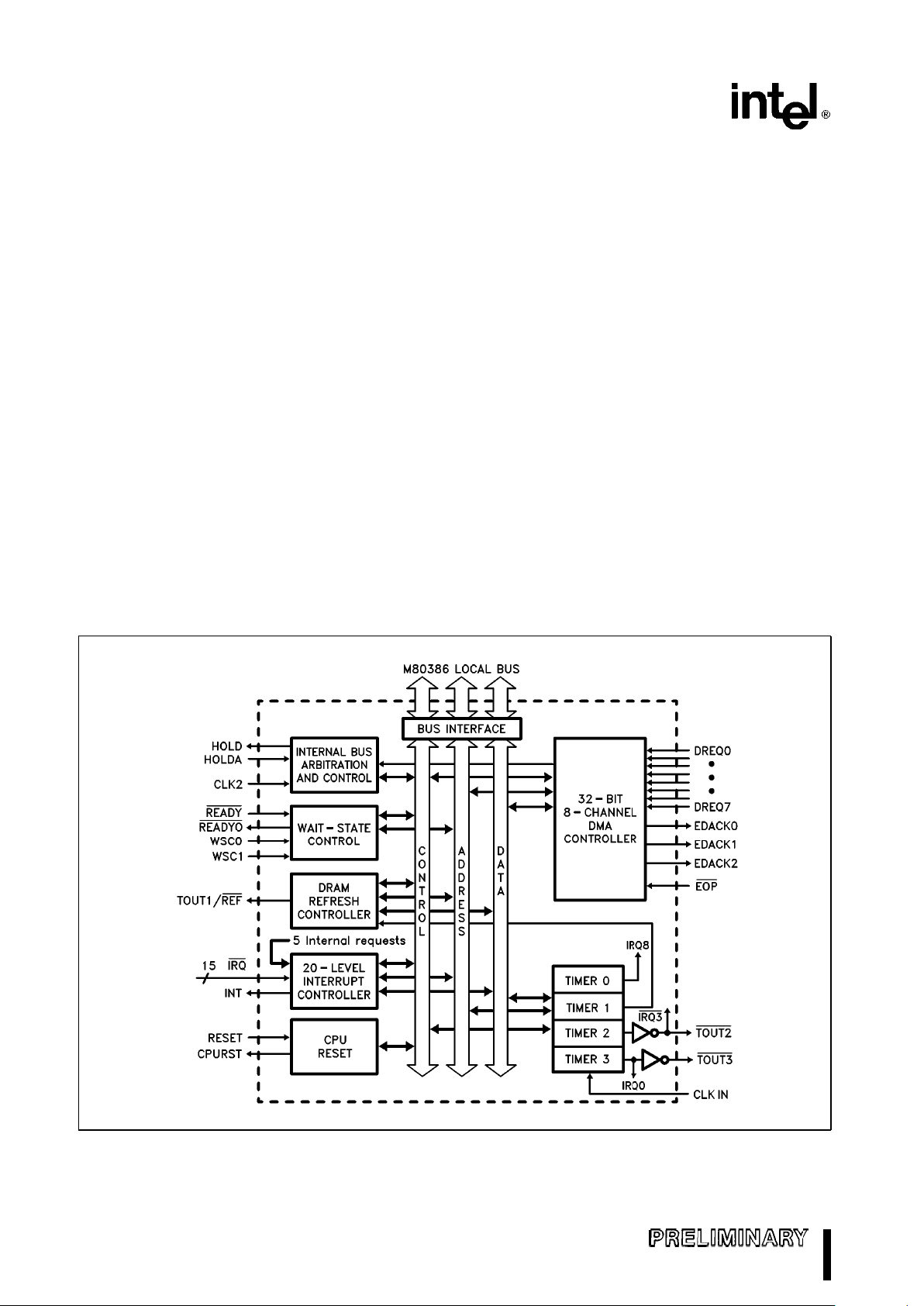
Figure 1 shows the basic architectural components
of the M82380. The following sections briefly discuss the architecture and function of each of the
distinct sections of the M82380.
271070–2
Figure 1. Architecture of the M82380
6
Page 7
M82380
1.1.1 DMA CONTROLLER
The M82380 contains a high-performance, 8-channel, 32-bit DMA controller. It is capable of transferring any combination of bytes, words, and double
words. The addresses of both source and destination can be independently incremented, decremented or held constant, and cover the entire 32-bit
physical address space of the i386 microprocessor.
It can disassemble and assemble misaligned data
via a 32-bit internal temporary data storage register.
Data transferred between devices of different data
path widths can also be assembled and disassembled using the internal temporary data storage register. The DMA Controller can also transfer aligned
data between I/O and memory on the fly, allowing
data transfer rates up to 32 megabytes per second
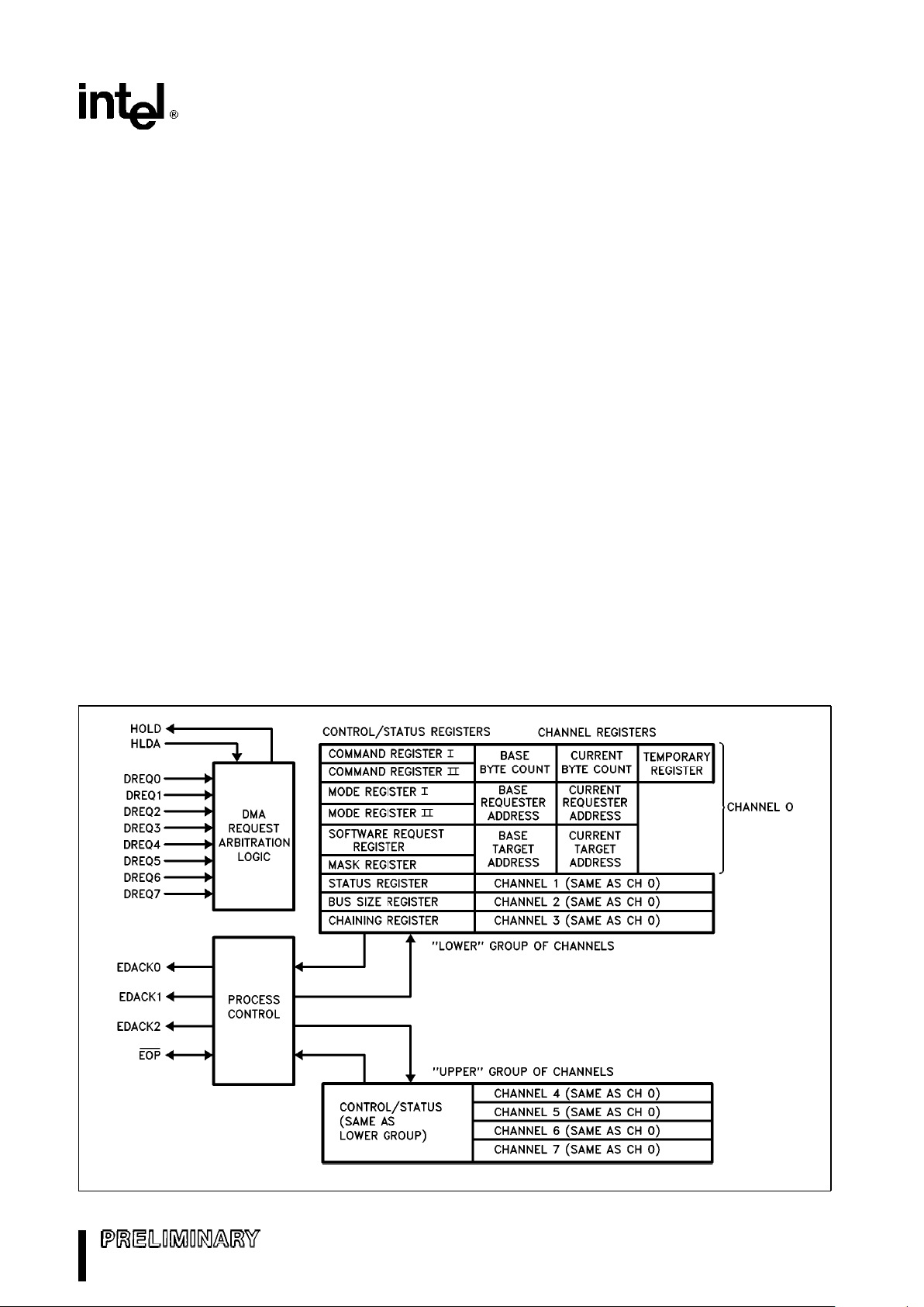
for an M82380 operating at 16 MHz. Figure 2 illustrates the functional components of the DMA Controller.
There are twenty-four general status and command
registers in the M82380 DMA Controller. Through
these registers any of the channels may be programmed into any of the possible modes. The operating modes of any one channel are independent of
the operation of the other channels.
Each channel has three programmable registers
which determine the location and amount of data to
be transferred:
Byte Count RegisterÐNumber of bytes to transfer. (24-bits)
Requester RegisterÐAddress of memory or peripheral which is requesting DMA service. (32bits)
Target RegisterÐAddress of peripheral or memory which will be accessed. (32-bits)
There are also port addresses which, when accessed, cause the M82380 to perform specific functions. The actual data written does not matter, the
act of writing to the specific address causes the
command to be executed. The commands which operate in this mode are: Master Clear, Clear Terminal
Count Interrupt Request, Clear Mask Register, and
Clear Byte Pointer Flip-Flop.
DMA transfers can be done between all combinations of memory and I/O; memory-to-memory, memory-to-I/O, I/O-to-memory, and I/O-to-I/O. DMA
service can be requested through software and/or
hardware. Hardware DMA acknowledge signals are
available for all channels (except channel 4) through
an encoded 3-bit DMA acknowledge bus
(EDACK0– 2).
271070–3
Figure 2. M82380 DMA Controller
7
Page 8
M82380
The M82380 DMA controller transfers blocks of data
(buffers) in three modes: Single Buffer, Buffer AutoInitialize, and Buffer Chaining. In the Single Buffer
Process, the M82380 DMA Controller is programmed to transfer one particular block of data.
Successive transfers then require reprogramming of
the DMA channel. Single Buffer transfers are useful
in systems where it is known at the time the transfer
begins what quantity of data is to be transferred, and
there is a contiguous block of data area available.
The Buffer Auto-Initialize Process allows the same
data area to be used for successive DMA transfers
without having to reprogram the channel.
The Buffer Chaining Process allows a program to
specify a list of buffer transfers to be executed. The
M82380 DMA Controller, through interrupt routines,
is reprogrammed from the list. The channel is reprogrammed for a new buffer before the current buffer
transfer is complete. This pipelining of the channel
programming process allows the system to allocate
non-contiguous blocks of data storage space, and
transfer all of the data with one DMA process. The
buffers that make up the chain do not have to be in
contiguous locations.
Channel priority can be fixed or rotating. Fixed priority allows the programmer to define the priority of
DMA channels based on hardware or other fixed parameters. Rotating priority is used to provide peripherals access to the bus on a shared basis.
With fixed priority, the programmer can set any
channel to have the current lowest priority. This al-
lows the user to reset or manually rotate the priority
schedule without reprogramming the command registers.
1.1.2 PROGRAMMABLE INTERVAL TIMERS
Four 16-bit programmable interval timers reside
within the M82380. These timers are identical in
function to the timers in the M82C54 Programmable
Interval Timer. All four of the timers share a common
clock input which can be independent of the system
clock. The timers are capable of operating in six different modes. In all of the modes, the current count
can be latched and read by the i386 processor at
any time, making these very versatile event timers.
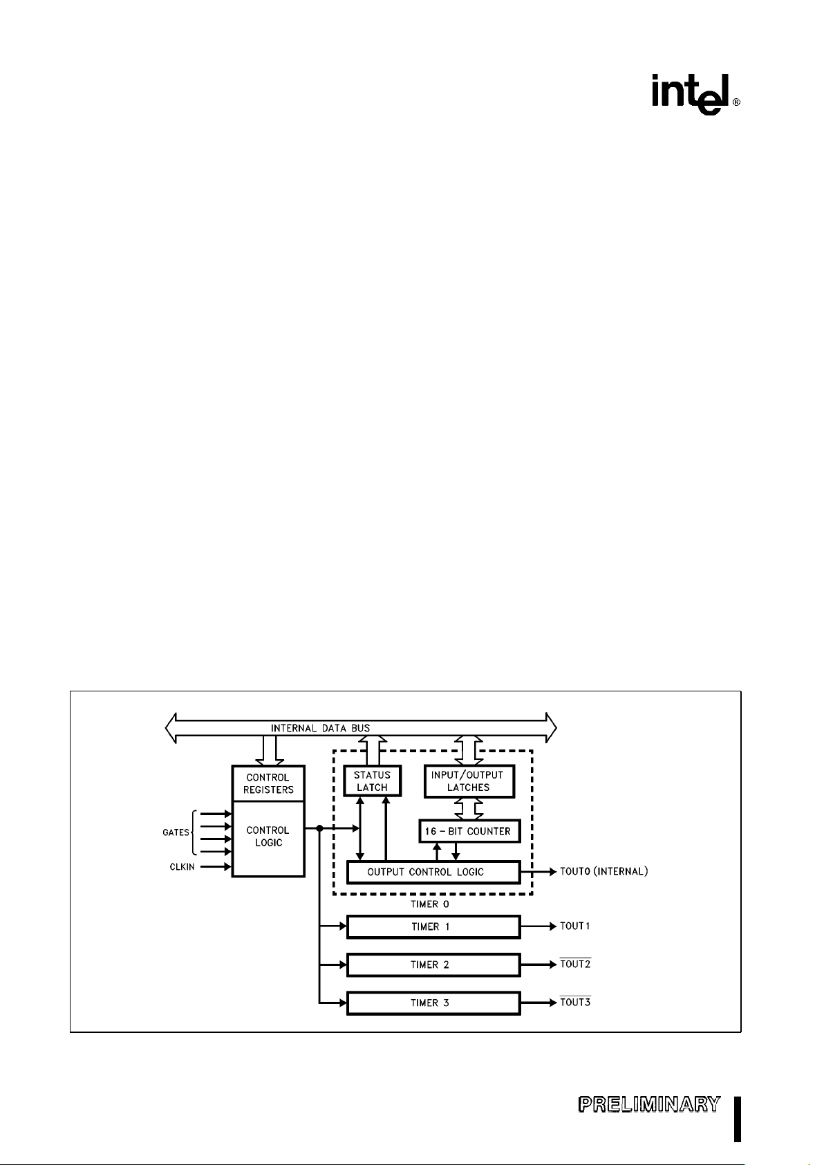
Figure 3 shows the functional components of the
Programmable Interval Timers.
The outputs of the timers are directed to key system
functions, making system design simpler. Timer 0 is
routed directly to an interrupt input and is not available externally. This timer would typically be used to
generate time-keeping interrupts.
Timers 1 and 2 have outputs which are available for
general timer/counter purposes as well as special
functions. Timer 1 is routed to the refresh control
logic to provide refresh timing. Timer 2 is connected
to an interrupt request input to provide other timer
functions. Timer 3 is a general purpose timer/counter whose output is available to external hardware. It
is also connected internally to the interrupt request
which defaults to the highest priority (IRQ0).
271070–4
Figure 3. Programmable Interval TimersÐBlock Diagram
8
Page 9
M82380
1.1.3 INTERRUPT CONTROLLER
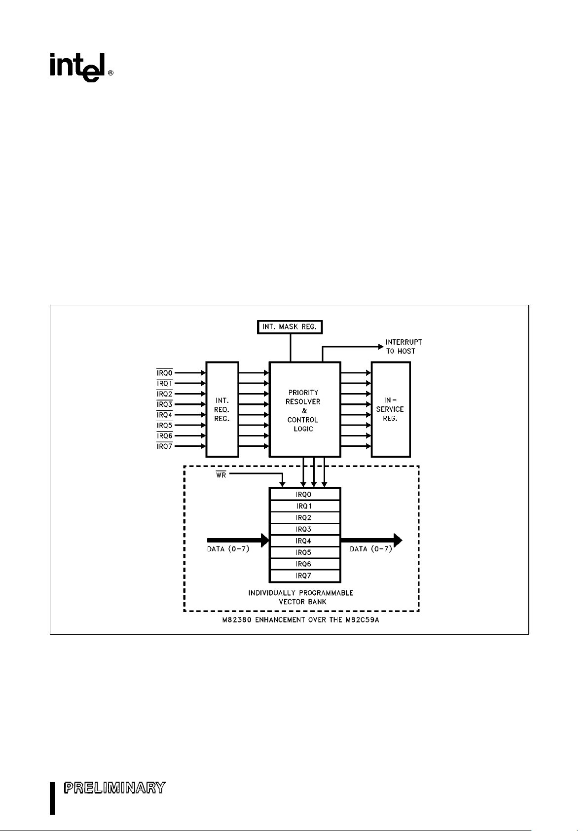
The M82380 has the equivalent of three enhanced
M8259A Programmable Interrupt Controllers. These
controllers can all be operated in the Master mode,
but the priority is always as if they were cascaded.
There are 15 interrupt request inputs provided for
the user, all of which can be inputs from external
slave interrupt controllers. Cascading M8259As to
these request inputs allows a possible total of 120
external interrupt requests. Figure 4 is a block diagram of the M82380 Interrupt Controller.
Each of the interrupt request inputs can be individually programmed with its own interrupt vector, allowing more flexibility in interrupt vector mapping than
was available with the M8259A. An interrupt is provided to alert the system that an attempt is being
made to program the vectors in the method of the
M8259A. This provides compatibility of existing software that used the M8259A with new designs using
the M82380.
In the event of an unrequested or otherwise erroneous interrupt acknowledge cycle, the M82380 Interrupt Controller issues a default vector. This vector,
programmed by the system software, will alert the
system of unsolicited interrupts of the M80386.
The functions of the M82380 Interrupt Controller are
identical to the M8259A, except in regards to programming the interrupt vectors as mentioned above.
Interrupt request inputs are programmable as either
edge or level triggered and are software maskable.
Priority can be either fixed or rotating and interrupt
requests can be nested.
271070–5
Figure 4. M82380 Interrupt ControllerÐBlock Diagram
9
Page 10
M82380
Enhancements are added to the M82380 for cascading external interrupt controllers. Master to Slave
handshaking takes place on the data bus, instead of
dedicated cascade lines.
1.1.4 WAIT STATE GENERATOR
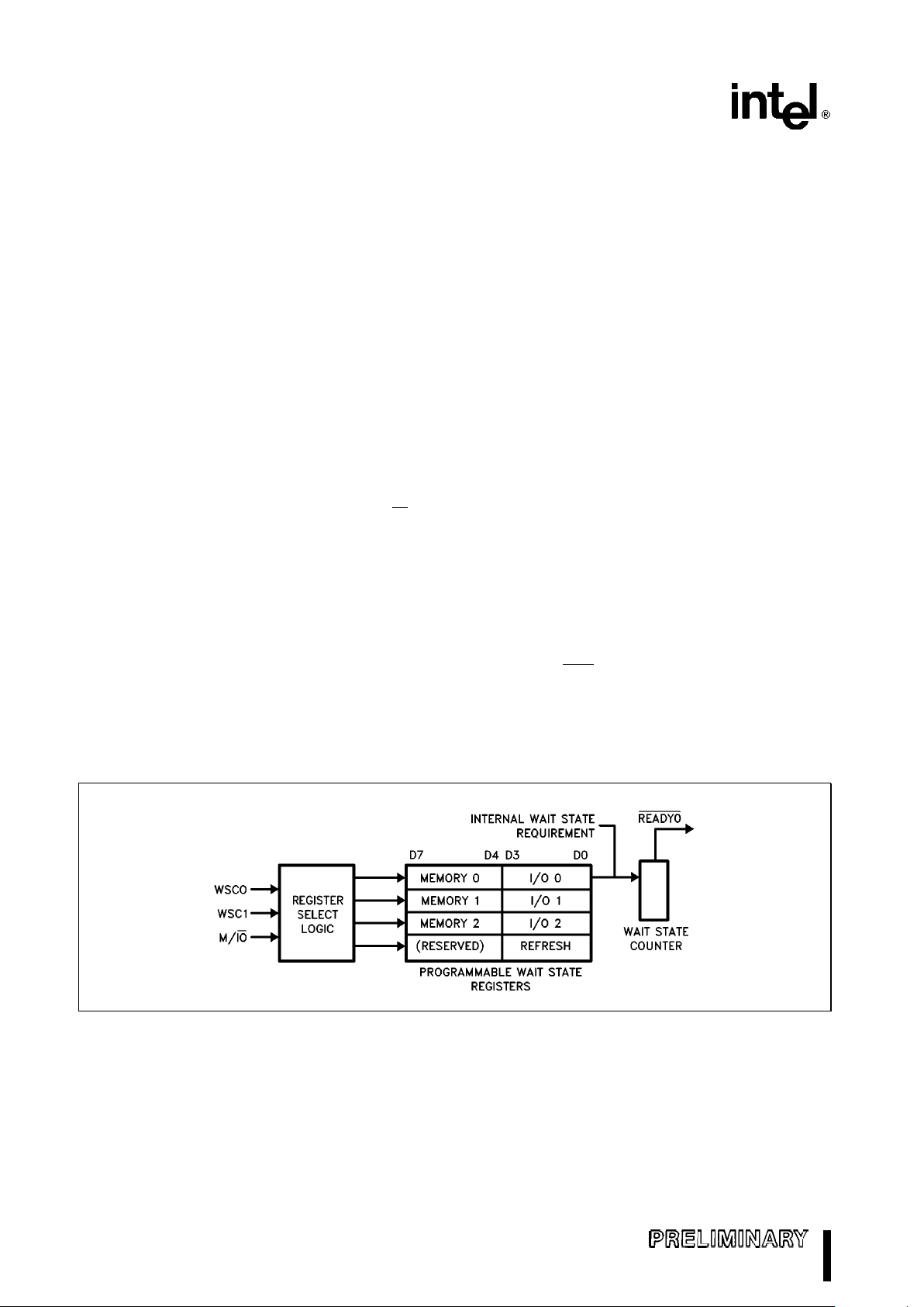
The Wait State Generator is a programmable
READY generation circuit for the i386 processor
bus. A peripheral requiring wait states can request
the Wait State Generator to hold the processor’s
READY input inactive for a predetermined number of
bus states. Six different wait state counts can be
programmed into the Wait State Generator by software; three for memory accesses and three for I/O
accesses. A block diagram of the M82380 Wait
State Generator is shown in Figure 5.
The peripheral being accessed selects the required
wait state count by placing a code on a 2-bit wait
state select bus. This code along with the M/IO
signal from the bus master is used to select one of six
internal 4-bit wait state registers which has been
programmed with the desired number of wait states.
From zero to fifteen wait states can be programmed
into the wait state registers. The Wait State Generator tracks the state of the processor or current bus
master at all times, regardless of which device is the
current bus master and regardless of whether or not
the Wait State Generator is currently active.
The M82380 Wait State Generator is disabled by
making the select inputs both high. This allows hardware which is intelligent enough to generate its own
ready signal to be accessed without penalty. As pre-
viously mentioned, deselecting the Wait State Generator does not disable its ability to determine the
proper number of wait states due to pipeline status
in subsequent bus cycles.
The number of wait states inserted into a pipelined
bus cycle is the value in the selected wait state register. If the bus master is operating in the non-pipelined mode, the Wait State Generator will increase
the number of wait states inserted into the bus cycle
by one.
On reset, the Wait State Generator’s registers are
loaded with the value FFH, giving the maximum
number of wait states for any access in which the
wait state select inputs are active.
1.1.5 DRAM REFRESH CONTROLLER
The M82380 DRAM Refresh Controller consists of a
24-bit refresh address counter and bus arbitration
logic. The output of Timer 1 is used to periodically
request a refresh cycle. When the controller receives the request, it requests access to the system
bus through the HOLD signal. When bus control is
acknowledged by the processor or current bus master, the refresh controller executes a memory read
operation at the address currently in the Refresh Address Register. At the same time, it activates a refresh signal (REF
) that the memory uses to force a
refresh instead of a normal read. Control of the bus
is transferred to the processor at the completion of
this cycle. Typically a refresh cycle will take six clock
cycles to execute on an i386 processor bus.
271070–6
Figure 5. M82380 Wait State GeneratorÐBlock Diagram
10
Page 11

M82380
The M82380 DRAM Refresh Controller has the highest priority when requesting bus access and will interrupt any active DMA process. This allows large
blocks of data to be moved by the DMA controller
without affecting the refresh function. Also the DMA
controller is not required to completely relinquish the
bus, the refresh controller simply steals a bus cycle
between DMA accesses.
The amount by which the refresh address is incremented is programmable to allow for different bus
widths and memory bank arrangements.
1.1.6 CPU RESET FUNCTION
The M82380 contains a special reset function which
can respond to hardware reset signals from the
M82384, as well as a software reset command. The
circuit will hold the i386 processor’s RESET line active while an external hardware reset signal is present at its RESET input. It can also reset the i386
processor as the result of a software command. The
software reset command causes the M82380 to
hold the processor’s RESET line active for a minimum of 62 CLK2 cycles; enough time to allow an
M80386 to re-initialize.
The M82380 can be programmed to sense the shutdown detect code on the status lines from the
M80386. If the Shutdown Detect function is enabled,
the M82380 will automatically reset the processor. A
diagnostic register is available which can be used to
determine the cause of reset.
1.1.7 REGISTER MAP RELOCATION
After a hardware reset, the internal registers of the
M82380 are located in I/O space beginning at port
address 0000H. The map of the M82380’s registers
is relocatable via a software command. The default
mapping places the M82380 between I/O addresses 0000H and 00DBH. The relocation register allows
this map to be moved to any even 256-byte boundary in the processor’s 16-bit I/O address space or any
even 16-Mbyte boundary in the 32-bit memory address space.
1.2 Host Interface
The M82380 is designed to operate efficiently on the
local bus of an M80386 microprocessor. The control
signals of the M82380 are identical in function to
those of the i386 processor. As a slave, the M82380
operates with all of the features available on the
i386 processor bus. When the M82380 is in the Master Mode, it looks identical to the i386 processor to
the connected devices.
The M82380 monitors the bus at all times, and determines whether the current bus cycle is a pipelined
or non-pipelined access. All of the status signals of
the processor are monitored.
The control, status, and data registers within the
M82380 are located at fixed addresses relative to
each other, but the group can be relocated to either
memory or I/O space and to different locations within those spaces.
As a Slave device, the M82380 monitors the control/status lines of the CPU. The M82380 will generate all of the wait states it needs whenever it is accessed. This allows the programmer the freedom of
accessing M82380 registers without having to insert
NOPs in the program to wait for slower M82380 internal registers.
The M82380 can determine if a current bus cycle is
a pipelined or a non-pipelined cycle. It does this by
monitoring the ADS
and READY signals and thereby
keeping track of the current state of the i386 processor.
As a bus master, the M82380 looks like an i386
processor to the rest of the system. This enables the
designer greater flexibility in systems which include
the M82380. The designer does not have to alter the
interfaces of any peripherals designed to operate
with the i386 processor to accommodate the
M82380. The M82380 will access any peripherals on
the bus in the same manner as the i386 processor,
including recognizing pipelined bus cycles.
The M82380 is accessed as an 8-bit peripheral. This
is done to maintain compatibility with existing system
architectures and software. The i386 processor
places the data of all 8-bit accesses either on D (0 –
7) or D (8 – 15). The M82380 will only accept data on
these lines when in the Slave Mode. When in the
Master Mode, the M82380 is a full 32-bit machine,
sending and receiving data in the same manner as
the i386 processor.
11
Page 12
M82380
2.0 i386TMPROCESSOR HOST
INTERFACE
The M82380 contains a set of interface signals to
operate efficiently with the i386 host processor.
These signals were designed so that minimal hardware is needed to connect the M82380 to the i386
processor.
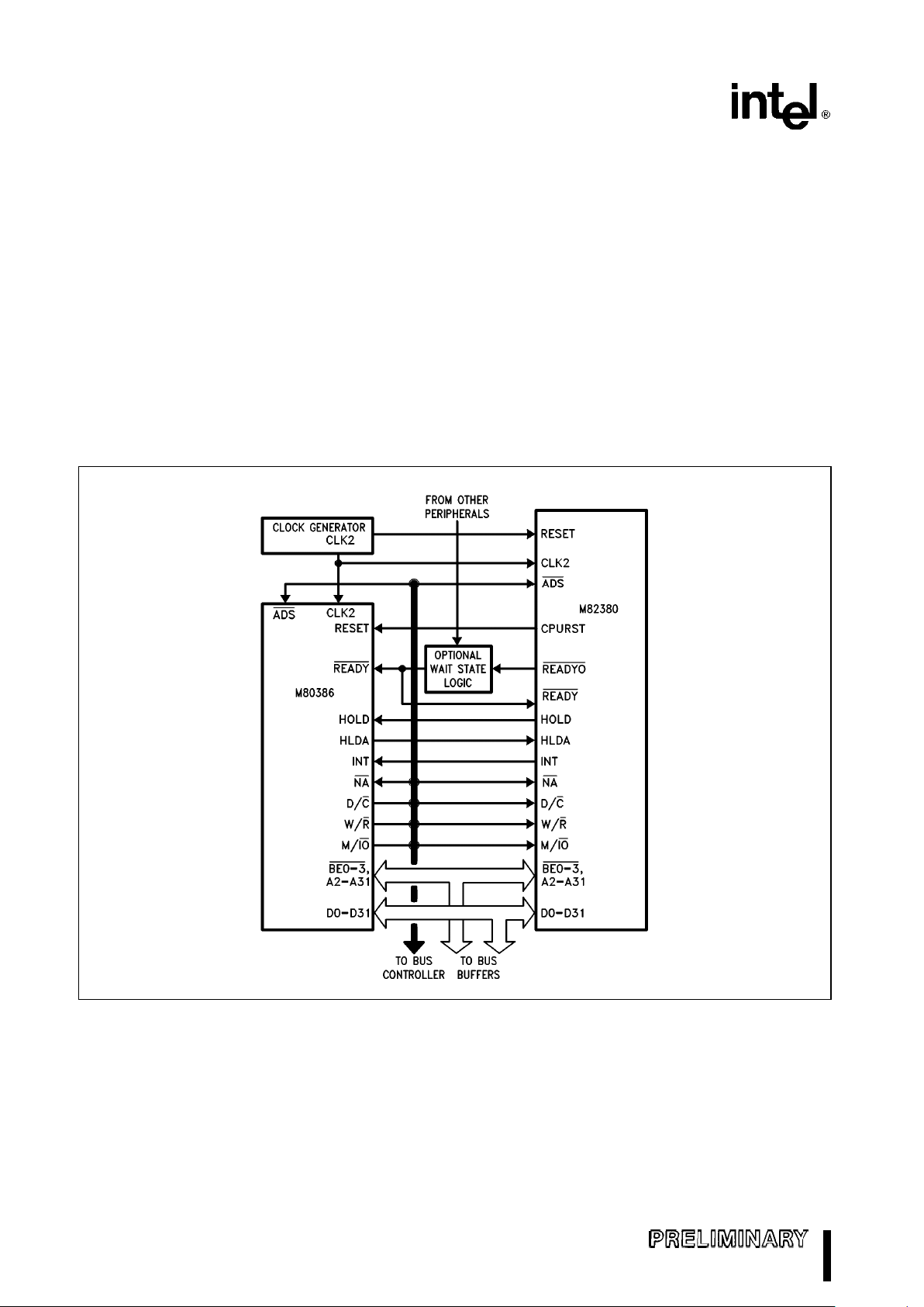
Figure 6 depicts a typical system configuration with
the i386 processor. As shown in the diagram, the
M82380 is designed to interface directly with the
i386 bus.
Since the M82380 is residing on the opposite side of
the data bus transceiver (with respect to the rest of
the peripherals in the system), it is important to note
that the transceiver should be controlled so that
contention between the data bus transceiver and
the M82380 will not occur. In order to do this, port
address decoding logic should be included in the direction and enable control logic of the transceiver.
When any of the M82380 internal registers is read,
the data bus transceiver should be disabled so that
only the M82380 will drive the local bus.
This section describes the basic bus functions of the
M82380 to show how this device interacts with the
i386 processor. Other signals which are not directly
related to the host interface will be discussed in their
associated functional block description.
271070–7
Figure 6. i386TM/M82380 System Configuration
12
Page 13
M82380
2.1 Master and Slave Modes
At any time, the M82380 acts as either a Slave device or a Master device in the system. Upon reset,
the M82380 will be in the Slave Mode. In this mode,
the i386 processor can read/write into the M82380
internal registers. Initialization information may be
programmed into the M82380 during Slave Mode.
When DMA service (including DRAM Refresh Cycles
generated by the M82380) is requested, the M82380
will request and subsequently get control of the i386
processor local bus. This is done through the HOLD
and HLDA (Hold Acknowledge) signals. When the
i386 processor responds by asserting the HLDA signal, the M82380 will switch into Master Mode and
perform DMA transfers. In this mode, the M82380 is
the bus master of the system. It can read/write data
from/to memory and peripheral devices. The
M82380 will return to the Slave Mode upon completion of DMA transfers, or when HLDA is negated.
2.2 M80386 INTERFACE SIGNALS
As mentioned in the Architecture section, the Bus
Interface module of the M82380 (see Figure 1) contains signals that are directly connected to the i386
host processor. This module has separate 32-bit
Data and Address busses. Also, it has additional
control signals to support different bus operations
on the system. By residing on the i386 processor
local bus, the M82380 shares the same address,
data and control lines with the processor. The following subsections discuss the signals which interface to the i386 host processor.
2.2.1 CLOCK (CLK2)
The CLK2 input provides fundamental timing for the
M82380. It is divided by two internally to generate
the M82380 internal clock. Therefore, CLK2 should
be driven with twice the i386’s frequency. In order to
maintain synchronization with the i386 host processor, the M82380 and the i386 processor should
share a common clock source.
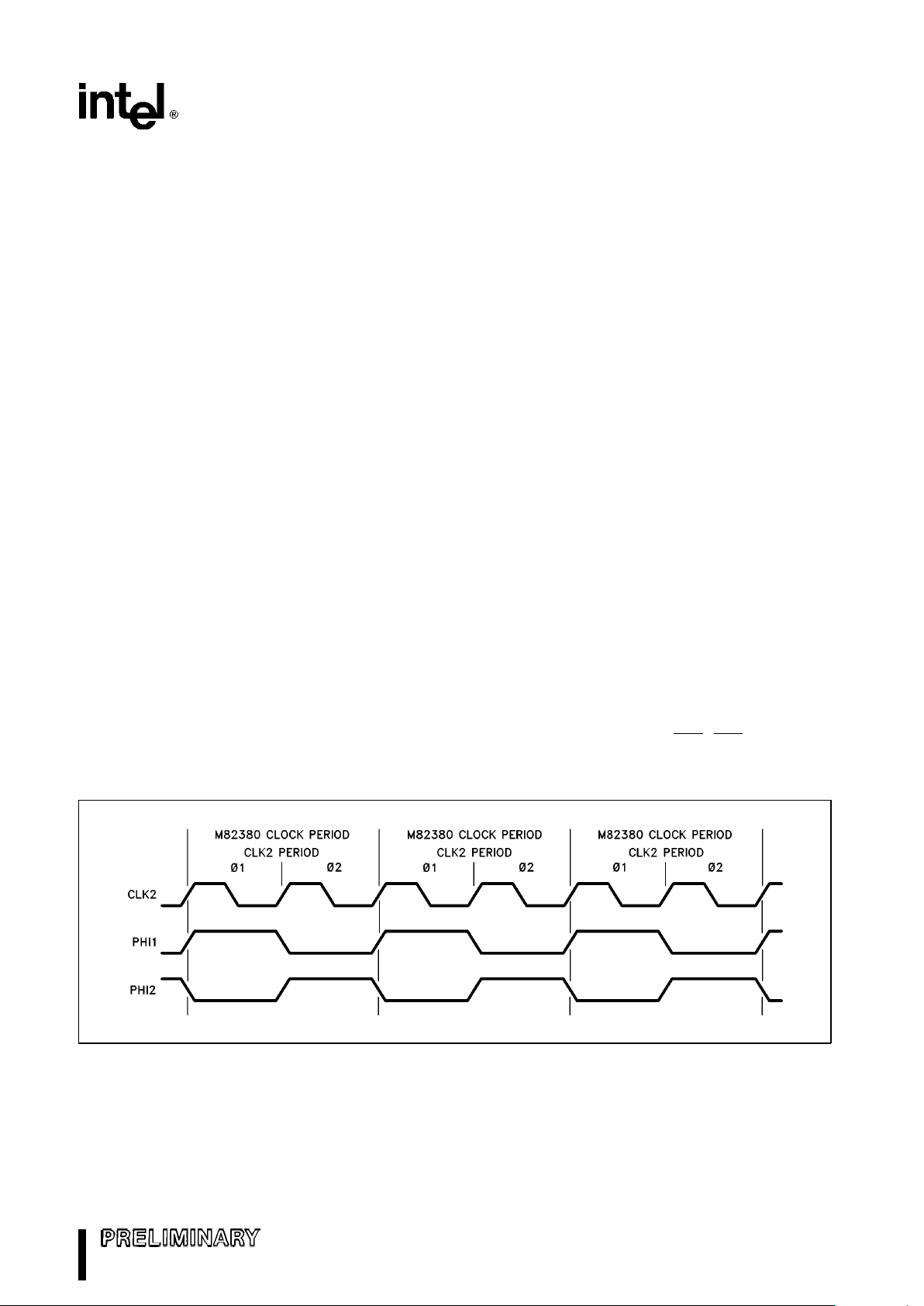
The internal clock consists of two phases: PHI1 and
PHI2. Each CLK2 period is a phase of the internal
clock. PHI2 is usually used to sample input and set
up internal signals and PHI1 is for latching internal
data. Figure 7 illustrates the relationship of CLK2
and the M82380 internal clock signals. The CPURST
signal generated by the M82380 guarantees that the
i386 processor will wake up in phase with PHI1.
2.2.2 DATA BUS (D0 –D31)
This 32-bit three-state bidirectional bus provides a
general purpose data path between the M82380 and
the system. These pins are tied directly to the corresponding Data Bus pins of the i386 processor local
bus. The Data Bus is also used for interrupt vectors
generated by the M82380 in the Interrupt Acknowledge cycle.
During Slave I/O operations, the M82380 expects a
single byte to be written or read. When the i386 host
processor writes into the M82380, either D0– D7 or
D8– D15 will be latched into the M82380, depending
upon how the Byte Enable (BE0
–BE3) signals are
driven. The M82380 does not need to look at D16 –
D31 since the i386 processor duplicates
271070–8
Figure 7. CLK2 and M82380 Internal Clock
13
Page 14

M82380
the single byte data on both halves of the bus. When
the M80386 host processor reads from the M82380,
the single byte data will be duplicated four times on
the Data Bus; i.e., on D0 –D7, D8– D15, D16– D23
and D24– D31.
During Master Mode, the M82380 can transfer 32-,
16-, and 8-bit data between memory (or I/O devices)
and I/O devices (or memory) via the Data Bus.
2.2.3 ADDRESS BUS (A31 –A2)
These three-state bidirectional signals are connected directly to the i386 Address Bus. In the Slave
Mode, they are used as input signals so that the
processor can address the M82380 internal ports/
registers. In the Master Mode, they are used as output signals by the M82380 to address memory and
peripheral devices. The Address Bus is capable of
addressing 4 G-bytes of physical memory space
(00000000H to FFFFFFFFH), and 64 K-bytes of I/O
addresses (00000000H to 0000FFFFH).
2.2.4 BYTE ENABLE (BE3
–BE0)
These bidirectional pins select specific byte(s) in the
double word addressed by A31–A2. Similar to the
Address Bus function, these signals are used as inputs to address internal M82380 registers during
Slave Mode operation. During Master Mode operation, they are used as outputs by the M82380 to address memory and I/O locations.
In addition to the above function, BE3
is used to
enable a production test mode and must be LOW
during reset. The i386 processor will automatically
hold BE3
LOW during RESET.
The definitions of the Byte Enable signals depend
upon whether the M82380 is in the Master or Slave
Mode. These definitions are depicted in Table 1.
Table 1. Byte Enable Signals
As INPUTS (Slave Mode):
BE3– BE0 Implied A1, A0
Data Bits Written
to M82380*
XXX0 00 D0– D7
XX01 01 D8 – D15
X011 10 D0– D7
X111 11 D8– D15
X–DON’T CARE
*During READ, data will be duplicated on D0 – D7, D8–D15, D16 – D23, and D24 – D31.
During WRITE, the M80386 host processor duplicates data on D0–D15, and D16 – D31, so that the
M82380 is concerned only with the lower half of the Data Bus.
As OUTPUTS (Master Mode):
Byte to be Accessed
Logical Byte Presented On
BE3
–BE0
Relative to A31– A2
Data Bus During WRITE Only*
D24–31 D16–23 D8–15 D0–7
1110 0 U U U A
1101 1 U U A A
1011 2 U A U A
0111 3 A U A A
1001 1, 2 U B A A
1100 0, 1 U U B A
0011 2, 3 B A B A
1000 0, 1, 2 U C B A
0001 1, 2, 3 C B A A
0000 0, 1, 2, 3 D C B A
UeUndefined
A
e
Logical D0 – D7
B
e
Logical D8 – D15
C
e
Logical D16 – D23
D
e
Logical D24 – D31
*Actual number of bytes accessed depends upon the programmed data path width.
14
Page 15

M82380
2.2.5 BUS CYCLE DEFINITION SIGNALS (D/C,
W/R
, M/IO)
These three-state bidirectional signals define the
type of bus cycle being performed. W/R
distin-
guishes between write and read cycles. D/C
distinguishes between processor data and control cycles.
M/IO
distinguishes between memory and I/O cy-
cles.
During Slave Mode, these signals are driven by the
i386 host processor; during Master Mode, they are
driven by the M82380. In either mode, these signals
will be valid when the Address Status (ADS
) is driven
LOW. Exact bus cycle definitions are given in Table
2. Note that some combinations are recognized as
inputs, but not generated as outputs. In the Master
Mode, D/C
is always HIGH.
2.2.6 ADDRESS STATUS (ADS)
This bidirectional signal indicates that a valid address (A2 – A31, BE0
–BE3) and bus cycle definition
(W/R
, D/C, M/IO) is being driven on the bus. In the
Master Mode, it is driven by the M82380 as an output. In the Slave Mode, this signal is monitored as an
input by the M82380. By the current and past status
of ADS and the READY input, the M82380 is able to
determine, during Slave Mode, if the next bus cycle
is a pipelined address cycle. ADS
is asserted during
T1 and T2P bus states (see Bus State Definition).
Note that during the idle states at the beginning and
the end of a DMA process, neither the i386 processor nor the M82380 is driving the ADS
signal; i.e.,
the signal is left floated. Therefore, it is important to
use a pull-up resistor (approximately 10 KX)onthe
ADS
signal.
2.2.7 TRANSFER ACKNOWLEDGE (READY
)
This input indicates that the current bus cycle is
complete. In the Master Mode, assertion of this signal indicates the end of a DMA bus cycle. In the
Slave Mode, the M82380 monitors this input and
ADS
to detect a pipelined address cycles. This sig-
nal should be tied directly to the READY
input of the
i386 host processor.
2.2.8 NEXT ADDRESS REQUEST (NA
)
This input is used to indicate to the M82380 in the
Master Mode that the system is requesting address
pipelining. When driven LOW by either memory or
peripheral devices during Master Mode, it indicates
that the system is prepared to accept a new address
and bus cycle definition signals from the M82380
before the end of the current bus cycle. If this input
is active when sampled by the M82380, the next address is driven onto the bus, provided a bus request
is already pending internally.
This input pin is monitored only in the Master Mode.
In the Slave Mode, the M82380 uses the ADS
and
READY
signals to determine address pipelining cy-
cles, and NA
will be ignored.
2.2.9 RESET (RESET, CPURST)
RESET
This synchronous input suspends any operation in
progress and places the M82380 in a known initial
state. Upon reset, the M82380 will be in the Slave
Mode waiting to be initialized by the i386 host
Table 2. Bus Cycle Definition
M/IO D/C W/R As INPUTS As OUTPUTS
0 0 0 Interrupt NOT GENERATED
Acknowledge
0 0 1 UNDEFINED NOT GENERATED
0 1 0 I/O Read I/O Read
0 1 1 I/O Write I/O Write
1 0 0 UNDEFINED NOT GENERATED
1 0 1 HALT if NOT GENERATED
BE(3–0)eX011
SHUTDOWN if
BE
(3–0)eXXX0
1 1 0 Memory Read Memory Read
1 1 1 Memory Write Memory Write
15
Page 16
M82380
Table 3. Output Signals Following RESET
Signal Level
A2– A31, D0–D31, BE0–BE3 Float
D/C
, W/R, M/IO, ADS Float
READYO
‘1’
EOP
‘1’ (Weak Pull-UP)
EDACK2– EDACK0 ‘100’
HOLD ‘0’
INT UNDEFINED*
TOUT1/REF, TOUT2/IRQ3, TOUT3 UNDEFINED*
CPURST ‘0’
*The Interrupt Controller and Programmable Interval Timer are initialized by software commands.
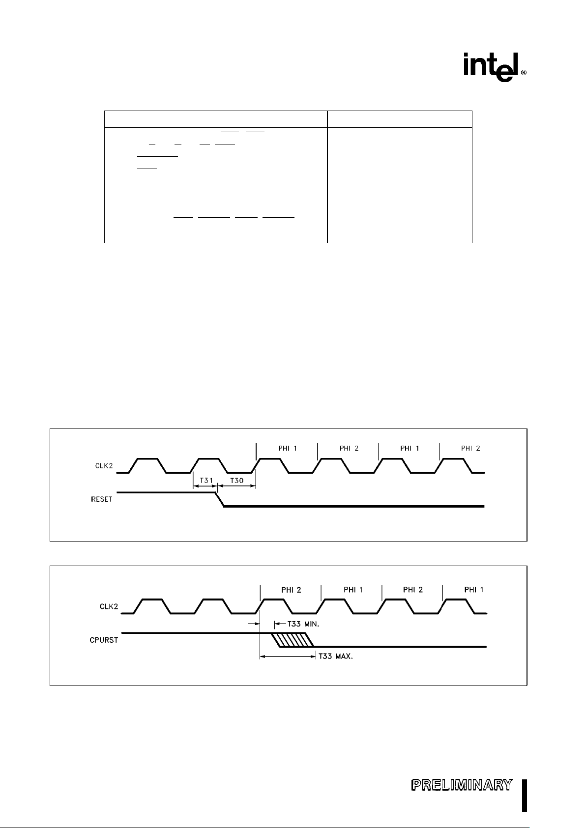
processor. The M82380 is reset by asserting RESET
for 15 or more CLK2 periods. When RESET is asserted, all other input pins are ignored, and all other
bus pins are driven to an idle bus state as shown in
Table 3. The M82380 will determine the phase of its
internal clock following RESET going inactive.
RESET is level-sensitive and must be synchronous
to the CLK2 signal. Therefore, this RESET input
should be tied to the RESET output of the Clock
Generator. The RESET setup and hold time requirements are shown in Figure 8.
CPURST
This output signal is used to reset the i386 host
processor. It will go active (HIGH) whenever one of
the following events occurs: a) M82380’s RESET input is active; b) a software RESET command is issued to the M82380; or c) when the M82380 detects
a processor Shutdown cycle and when this detection feature is enabled (see CPU Reset and Shutdown Detect). When activated, CPURST will be held
active for 62 CLK2 periods. The timing of CPURST is
such that the i386 processor will be in synchronization with the M82380. This timing is shown in
Figure 9.
271070–9
T30-RESET Hold Time
T31-RESET Setup Time
Figure 8. RESET Timing
271070–10
T33-CPU Reset from CLK2
Figure 9. CPURST Timing
16
Page 17

M82380
2.2.10 INTERRUPT OUT (INT)
This output pin is used to signal the i386 host processor that one or more interrupt requests (either internal or external) are pending. The processor is expected to respond with an Interrupt Acknowledge
cycle. This signal should be connected directly to
the Maskable Interrupt Request (INTR) input of the
i386 host processor.
2.3 M82380 Bus Timing
The M82380 internally divides the CLK2 signal by
two to generate its internal clock. Figure 7 shows the
relationship of CLK2 and the internal clock. The internal clock consists of two phases: PHI1 and PHI2.
Each CLK2 period is a phase of the internal clock. In
Figure 7, both PHI1 and PHI2 of the M82380 internal
clock are shown.
In the M82380, whether it is in the Master or Slave
Mode, the shortest time unit of bus activity is a bus
state. A bus state, which is also referred as a
‘T-state’, is defined as one M82380 PHI2 clock period (i.e., two CLK2 periods). Recall in Table 2, there
are six different types of bus cycles in the M82380
as defined by the M/IO
, D/C and W/R signals. Each
of these bus cycles is composed of two or more bus
states. The length of a bus cycle depends on when
the READY
input is asserted (i.e., driven LOW).
2.3.1 ADDRESS PIPELINING
The M82380 supports Address Pipelining as an option in both the Master and Slave Mode. This feature
typically allows a memory or peripheral device to operate with one less wait state than would otherwise
be required. This is possible because during a pipelined cycle, the address and bus cycle definition of
the next cycle will be generated by the bus master
while waiting for the end of the current cycle to be
acknowledged. The pipelined bus is especially well
suited for interleaved memory environment. For
16 MHz interleaved memory designs with 100 ns access time DRAMs, zero wait state memory accesses
can be achieved when pipelined addressing is selected.
In the Master Mode, the M82380 is capable of initiating, on a cycle-by-cycle basis, either a pipelined or
non-pipelined access depending upon the state of
the NA
input. If a pipelined cycle is requested (indi-
cated by NA
being driven LOW), the M82380 will
drive the address and bus cycle definition of the next
cycle as soon as there is an internal bus request
pending.
In the Slave Mode, the M82380 is constantly monitoring the ADS
and READY signals on the processor
local bus to determine if the current bus cycle is a
pipelined cycle. If a pipelined cycle is detected, the
M82380 will request one less wait state from the
processor if the Wait State Generator feature is selected. On the other hand, during an M82380 internal register access in a pipelined cycle, it will make
use of the advance address and bus cycle information. In all cases, Address Pipelining will result in a
savings of one wait state.
2.3.2 MASTER MODE BUS TIMING
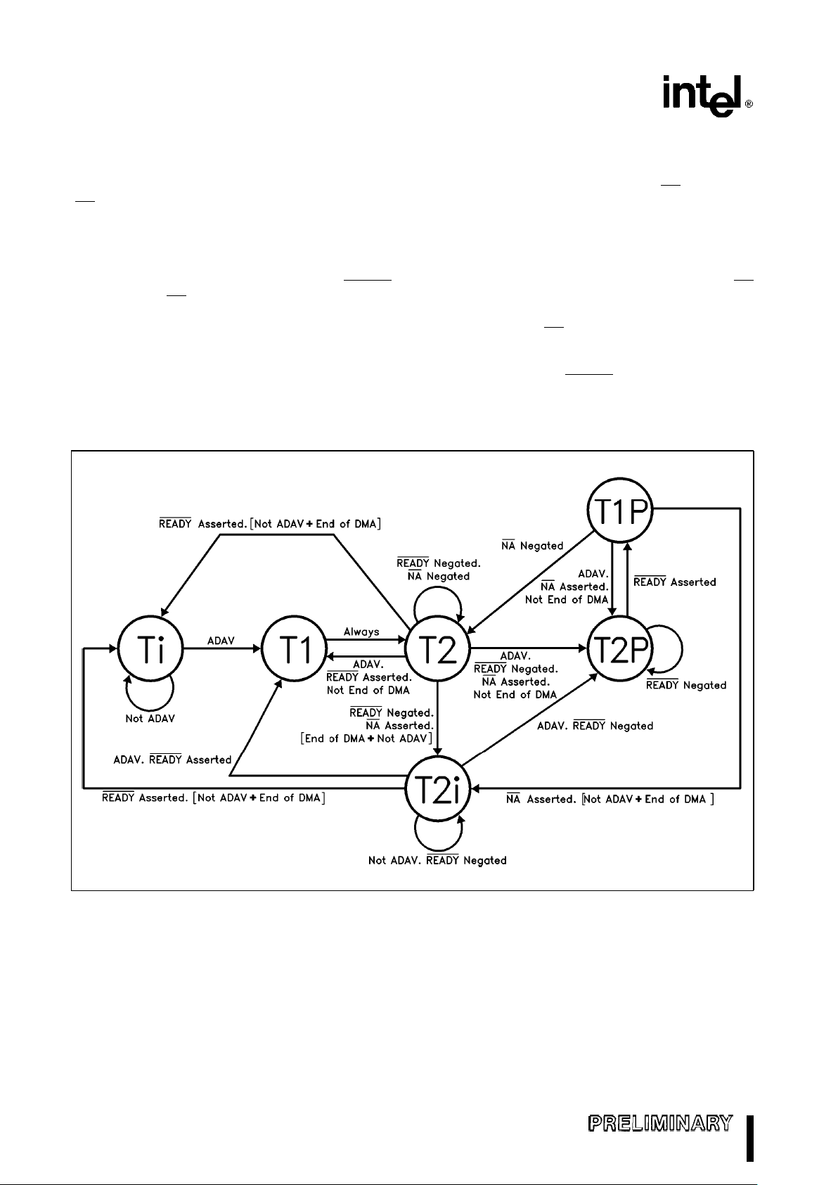
When the M82380 is in the Master Mode, it will be in
one of six bus states. Figure 10 shows the complete
bus state diagram of the Master Mode, including
pipelined address states. As seen in the figure, the
M82380 state diagram is very similar to that of the
i386 processor. The major difference is that in the
M82380, there is no Hold state. Also, in the M82380,
the conditions for some state transitions depend
upon whether it is the end of a DMA process.
NOTE:
The term ‘end of a DMA process’ is loosely defined
here. It depends on the DMA modes of operation
as well as the state of the EOP
and DREQ inputs.
This is explained in detail in section 3ÐDMA Controller.
17
Page 18
M82380
The M82380 will enter the idle state, Ti, upon RESET and whenever the internal address is not available at the end of a DMA cycle or at the end of a
DMA process. When address pipelining is not used
(NA
is not asserted), a new bus cycle always begins
with state T1. During T1, address and bus cycle definition signals will be driven on the bus. T1 is always
followed by T2.
If a bus cycle is not acknowledged (with READY
)
during T2 and NA
is negated, T2 will be repeated.
When the end of the bus cycle is acknowledged during T2, the following state will be T1 of the next bus
cycle (if the internal address latch is loaded and if
this is not the end of the DMA process). Otherwise,
the Ti state will be entered. Therefore, if the memory
or peripheral accessed is fast enough to respond
within the first T2, the fastest non-pipelined cycle will
take one T1 and one T2 state.
Use of the address pipelining feature allows the
M82380 to enter three additional bus states: T1P,
T2P, and T2i. T1P is the first bus state of a pipelined
bus cycle. T2P follows T1P (or T2) if NA
is asserted
when sampled. The M82380 will drive the bus with
the address and bus cycle definition signals of the
next cycle during T2P. From the state diagram, it can
be seen that after an idle state Ti, the first bus cycle
must begin with T1, and is therefore a non-pipelined
bus cycle. The next bus cycle can be pipelined if NA
is asserted and the previous bus cycle ended in a
T2P state. Once the M82380 is in a pipelined cycle
and provided that NA
is asserted in subsequent cycles, the M82380 will be switching between T1P and
T2P states. If the end of the current bus cycle is not
acknowledged by the READY
input, the M82380 will
extend the cycle by adding T2P states. The fastest
pipelined cycle will consist of one T1P and one T2P
state.
271070–11
NOTE:
ADAVÐInternal Address Available
Figure 10. Master Mode State Diagram
18
Page 19
M82380
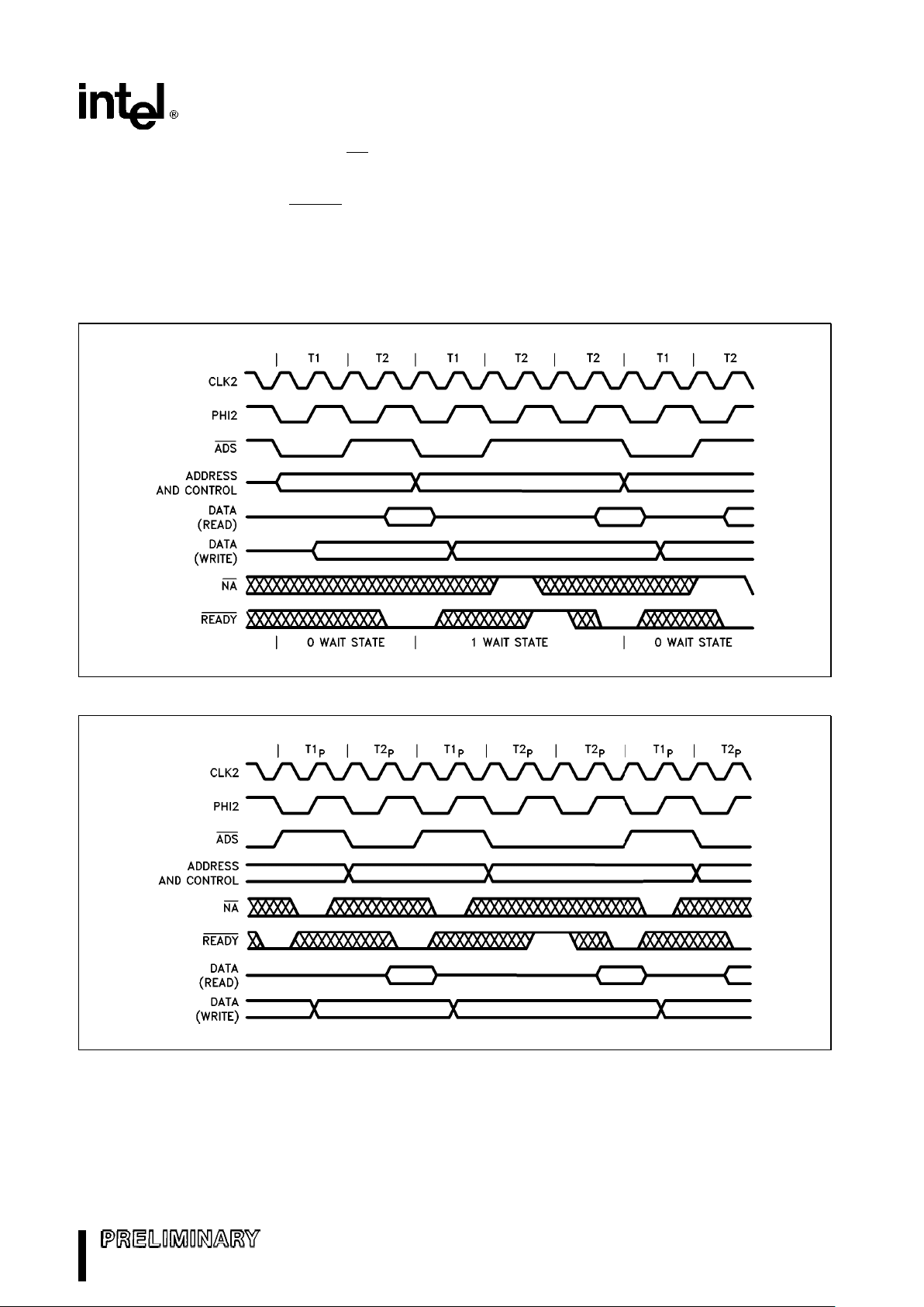
The M82380 will enter state T2i when NA is asserted and when one of the following two conditions
occurs. The first condition is when the M82380 is in
state T2. T2i will be entered if READY
is not asserted and there is no next address available. This situation is similar to a wait state. The M82380 will stay in
T2i for as long as this condition exists. The second
condition which will cause the M82380 enter T2i is
when the M82380 is in state T1P. Before going to
state T2P, the M82380 needs to wait in state T2i
until the next address is available. Also, in both cases, if the DMA process is complete, the M82380 will
enter the T2i state in order to finish the current DMA
cycle.
Figure 11 is a timing diagram showing non-pipelined
bus accesses in the Master Mode. Figure 12 shows
the timing of pipelined accesses in the Master Mode.
271070–12
Figure 11. Non-Pipelined Bus Cycles
271070–13
Figure 12. Pipelined Bus Cycles
19
Page 20
M82380
2.3.3 SLAVE MODE BUS TIMING
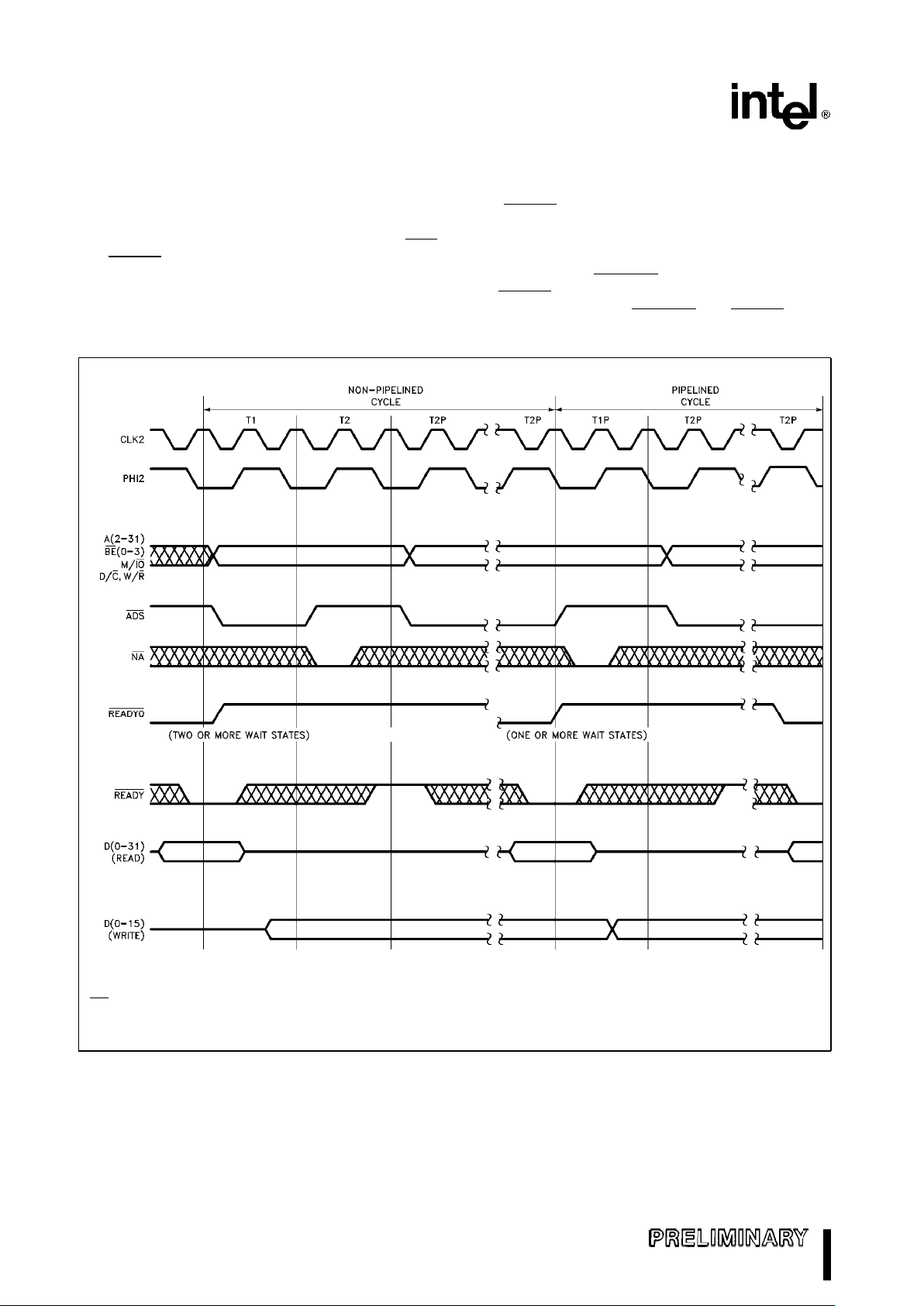
Figure 13 shows the Slave Mode bus timing in both
pipelined and non-pipelined cycles when the
M82380 is being accessed. Recall that during Slave
Mode, the M82380 will constantly monitor the ADS
and READY signals to determine if the next cycle is
pipelined. In Figure 13, the first cycle is non-pipelined and the second cycle is pipelined. In the pipelined cycle, the M82380 will start decoding the ad-
dress and bus cycle signals one bus state earlier
than in a non-pipelined cycle.
The READY
input signal is sampled by the M80386
host processor to determine the completion of a bus
cycle. This occurs during the end of every T2 and
T2P state. Normally, the output of the M82380 Wait
State Generator, READYO
, is directly connected to
the READY
input of the i386 host processor and the
M82380. In such case, READYO
and READY will be
identical (see Wait State Generator).
271070–14
NOTE:
NA
is shown here only for timing reference. It is not sampled by the M82380 during Slave Mode.
When the M82380 registers are accessed, it will take one or more wait states in pipelined and two or more wait states in
non-pipelined cycle to complete the internal access.
Figure 13. Slave Read/Write Timing
20
Page 21
M82380
3.0 DMA CONTROLLER
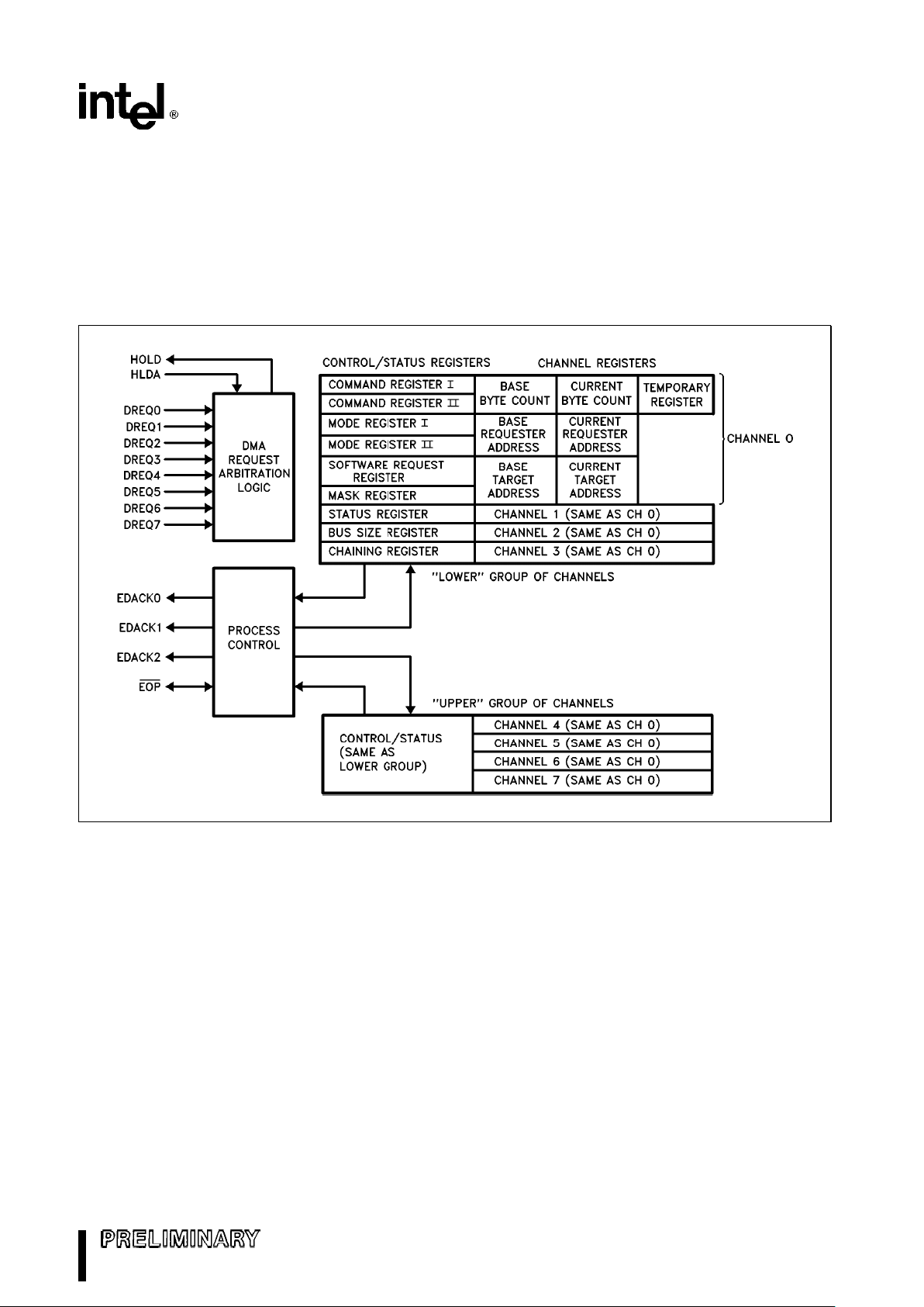
The M82380 DMA Controller is capable of transferring data between any combination of memory and/
or I/O, with any combination (8-, 16-, or 32-bits) of
data path widths. Bus bandwidth is optimized
through the use of an internal temporary register
which can disassemble or assemble data to or from
either an aligned or a non-aligned destination or
source. Figure 14 is a block diagram of the M82380
DMA Controller.
The M82380 has eight channels of DMA. Each
channel operates independently of the others. Within the operation of the individual channels, there are
many different modes of data transfer available.
Many of the operating modes can be intermixed to
provide a very versatile DMA controller.
271070–15
Figure 14. M82380 DMA Controller Block Diagram
21
Page 22

M82380
3.1 Functional Description
In describing the operation of the M82380’s DMA
Controller, close attention to terminology is required.
Before entering the discussion of the function of the
M82380 DMA Controller, the following explanations
of some of the terminology used herein may be of
benefit. First, a few terms for clarification:
DMA PROCESSÐA DMA process is the execution
of a programmed DMA task from beginning to end.
Each DMA process requires initial programming by
the host M80386 microprocessor.
BUFFERÐA contiguous block of data.
BUFFER TRANSFERÐThe action required by the
DMA to transfer an entire buffer.
DATA TRANSFERÐThe DMA action in which a
group of bytes, words, or double words are moved
between devices by the DMA Controller. A data
transfer operation may involve movement of one or
many bytes.
BUS CYCLEÐAccess by the DMA to a single byte,
word, or double word.
Each DMA channel consists of three major components. These components are identified by the contents of programmable registers which define the
memory or I/O devices being serviced by the DMA.
They are the Target, the Requester, and the Byte
Count. They will be defined generically here and in
greater detail in the DMA register definition section.
The Requester is the device which requires service
by the M82380 DMA Controller, and makes the request for service. All of the control signals which the
DMA monitors or generates for specific channels
are logically related to the Requester. Only the Requester is considered capable of initiating or terminating a DMA process.
The Target is the device with which the Requester
wishes to communicate. As far as the DMA process
is concerned, the Target is a slave which is incapable of control over the process.
The direction of data transfer can be either from Requester to Target or from Target to Requester; i.e.,
each can be either a source or a destination.
The Requester and Target may each be either I/O
or memory. Each has an address associated with it
that can be incremented, decremented, or held constant. The addresses are stored in the Requester
Address Registers and Target Address Registers,
respectively. These registers have two parts: one
which contains the current address being used in the
DMA process (Current Address Register), and one
which holds the programmed base address (Base
Address Register). The contents of the Base Registers are never changed by the M82380 DMA Controller. The Current Registers are incremented or
decremented according to the progress of the DMA
process.
The Byte Count is the component of the DMA process which dictates the amount of data which must
be transferred. Current and Base Byte Count Registers are provided. The Current Byte Count Register
is decremented once for each byte transferred by
the DMA process. When the register is decremented
past zero, the Byte Count is considered ‘expired’
and the process is terminated or restarted, depending on the mode of operation of the channel. The
point at which the Byte Count expires is called ‘Terminal Count’ and several status signals are dependent on this event.
Each channel of the M82380 DMA Controller also
contains a 32-bit Temporary Register for use in assembling and disassembling non-aligned data. The
operation of this register is transparent to the user,
although the contents of it may affect the timing of
some DMA handshake sequences. Since there is
data storage available for each channel, the DMA
Controller can be interrupted without loss of data.
The M82380 DMA Controller is a slave on the bus
until a request for DMA service is received via either
a software request command or a hardware request
signal. The host processor may access any of the
control/status or channel registers at any time the
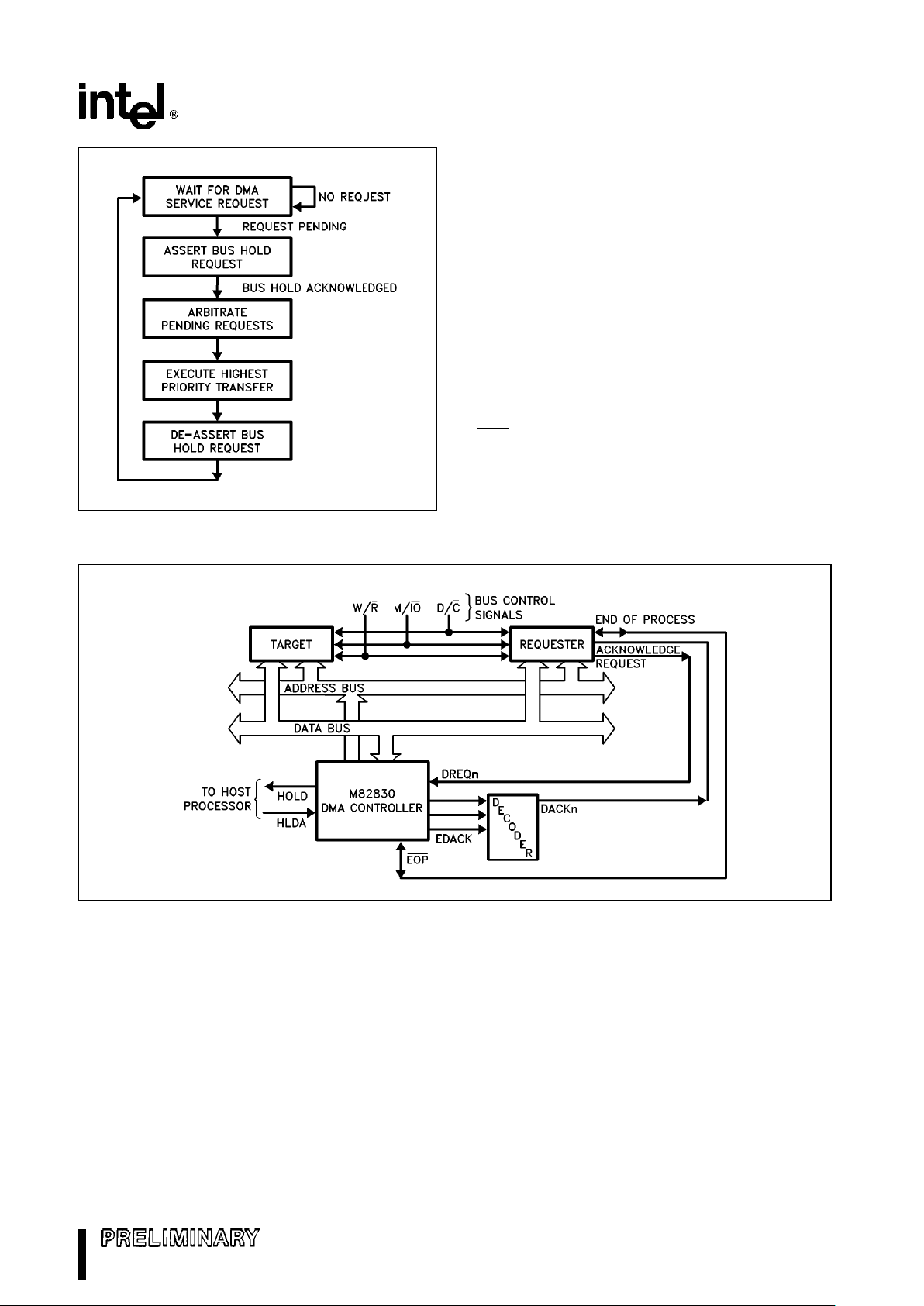
M82380 is a bus slave. Figure 15 shows the flow of
operations that the DMA Controller performs.
At the time a DMA service request is received, the
DMA Controller issues a bus hold request to the
host processor. The M82380 becomes the bus master when the host relinquishes the bus by asserting a
hold acknowledge signal. The channel to be serviced will be the one with the highest priority at the
time the DMA Controller becomes the bus master.
The DMA Controller will remain in control of the bus
until the hold acknowledge signal is removed, or until the current DMA transfer is complete.
While the M82380 DMA Controller has control of the
bus, it will perform the required data transfer(s). The
type of transfer, source and destination addresses,
and amount of data to transfer are programmed in
the control registers of the DMA channel which received the request for service.
22
Page 23
M82380
271070–16
Figure 15. Flow of DMA Controller Operation
At completion of the DMA process, the M82380 will
remove the bus hold request. At this time the
M82380 becomes a slave again, and the host returns to being a master. If there are other DMA
channels with requests pending, the controller will
again assert the hold request signal and restart the
bus arbitration and switching process.
3.2 Interface Signals
There are fourteen control signals dedicated to the
DMA process. They include eight DMA Channel Requests (DREQn), three Encoded DMA Acknowledge
signals (EDACKn), Processor Hold and Hold Acknowledge (HOLD, HLDA), and End-Of-Process
(EOP
). The DREQn inputs and EDACK(0 –2) outputs
are handshake signals to the devices requiring DMA
service. The HOLD output and HLDA input are handshake signals to the host processor. Figure 16
shows these signals and how they interconnect between the M82380 DMA Controller, and the Requester and Target devices.
271070–17
Figure 16. Requester, Target, and DMA Controller Interconnection
23
Page 24

M82380
3.2.1 DREQn and EDACK(0 –2)
These signals are the handshake signals between
the peripheral and the M82380. When the peripheral
requires DMA service, it asserts the DREQn signal
of the channel which is programmed to perform the
service. The M82380 arbitrates the DREQn against
other pending requests and begins the DMA process after finishing other higher priority processes.
When the DMA service for the requested channel is
in progress, the EDACK(0– 2) signals represent the
DMA channel which is accessing the Requester.
The 3-bit code on the EDACK(0 – 2) lines indicates
the number of the channel presently being serviced.
Table 4 shows the encoding of these signals. Note
that Channel 4 does not have a corresponding hardware acknowledge.
The DMA acknowledge (EDACK) signals indicate
the active channel only during DMA accesses to the
Requester. During accesses to the Target,
EDACK(0– 2) has the idle code (100). EDACK(0– 2)
can thus be used to select a Requester device during a transfer.
Table 4. EDACK Encoding
During a DMA Transfer
EDACK2 EDACK1 EDACK0 Active Channel
000 0
001 1
010 2
011 3
1 0 0 Target Access
101 5
110 6
111 7
DREQn can be programmed as either an Asynchronous or Synchronous input.
The EDACKn signals are always active. They either
indicate ‘no acknowledge’ or they indicate a bus access to the requester. The acknowledge code is either 100, for an idle DMA or during a DMA access to
the Target, or ‘n’ during a Requester access, where
n is the binary value representing the channel. A
simple 3-line to 8-line decoder can be used to provide discrete acknowledge signals for the peripherals.
3.2.2 HOLD and HLDA
The Hold Request (HOLD) and Hold Acknowledge
(HLDA) signals are the handshake signals between
the DMA Controller and the host processor. HOLD is
an output from the M82380 and HLDA is an input.
HOLD is asserted by the DMA Controller when there
is a pending DMA request, thus requesting the processor to give up control of the bus so the DMA process can take place. The M80386 responds by asserting HLDA when it is ready to relinquish control of
the bus.
The M82380 will begin operations on the bus one
clock cycle after the HLDA signal goes active. For
this reason, other devices on the bus should be in
the slave mode when HLDA is active.
HOLD and HLDA should not be used to gate or select peripherals requesting DMA service. This is because of the use of DMA-like operations by the
DRAM Refresh Controller. The Refresh Controller is
arbitrated with the DMA Controller for control of the
bus, and refresh cycles have the highest priority. A
refresh cycle will take place between DMA cycles
without relinquishing bus control. See the Arbitration
of Refresh Requests for a more detailed discussion
of the interaction between the DMA Controller and
the DRAM Refresh Controller.
3.2.3 EOP
EOP is a bidirectional signal used to indicate the end
of a DMA process. The M82380 activates this as an
output during the T2 states of the last Requester bus
cycle for which a channel is programmed to execute.
The Requester should respond by either withdrawing its DMA request, or interrupting the host processor to indicate that the channel needs to be programmed with a new buffer. As an input, this signal
is used to tell the DMA Controller that the peripheral
being serviced does not require any more data to be
transferred. This indicates that the current buffer is
to be terminated.
EOP
can be programmed as either an Asynchronous or a Synchronous input. Details on synchronous versus asynchronous operation of this pin are
described later in this data sheet.
3.3 Modes of Operation
The M82380 DMA Controller has many independent
operating functions. When designing peripheral interfaces for the M82380 DMA Controller, all of the
functions or modes must be considered. All of the
channels are independent of each other (except in
priority of operation) and can operate in any of the
modes. Many of the operating modes, though independently programmable, affect the operation of
other modes. Because of the large number of com-
24
Page 25

M82380
binations possible, each programmable mode is discussed here with its affects on the operation of other
modes. The entire list of possible combinations will
not be presented.
Table 5 shows the categories of DMA features available in the M82380. Each of the five major
categories is independent of the others. The subcategories are the available modes within the major
function or mode category. The following sections
explain each mode or function and its relation to other features.
Table 5. DMA Operating Modes
I. Target/Requester Definition
a. Data Transfer Direction
b. Device Type
c. Increment/Decrement/Hold
II. Buffer Processes
a. Single Buffer Process
b. Buffer Auto-Initialize Process
c. Buffer Chaining Process
III. Data Transfer/Handshake Modes
a. Single Transfer Mode
b. Demand Transfer Mode
c. Block Transfer Mode
d. Cascade Mode
IV. Priority Arbitration
a. Fixed
b. Rotating
c. Programmable Fixed
V. Bus Operation
a. Fly-By (Single-Cycle)/Two-Cycle
b. Data Path Width
c. Read, Write, or Verify Cycles
3.3.1 TARGET/REQUESTER DEFINITION
All DMA transfers involve three devices: the DMA
Controller, the Requester, and the Target. Since the
devices to be accessed by the DMA Controller vary
widely, the operating characteristics of the DMA
Controller must be tailored to the Requester and
Target devices.
The Requester can be defined as either the source
or the destination of the data to be transferred. This
is done by specifying a Write or a Read transfer,
respectively. In a Read transfer, the Target is the
data source and the Requester is the destination for
the data. In a Write transfer, the Requester is the
source and the Target in the destination.
The Requester and Target addresses can each be
independently programmed to be incremented, decremented, or held constant. As an example, the
M82380 is capable of reversing a string or data by
having a Requester address increment and the Target address decrement in a memory-to-memory
transfer.
3.3.2 BUFFER TRANSFER PROCESSES
The M82380 DMA Controller allows three programmable Buffer Transfer Processes. These processes
define the logical way in which a buffer of data is
accessed by the DMA.
The three Buffer Transfer Processes include the Single Buffer Process, the Buffer Auto-Initialize Process, and the Buffer Chaining Process. These processes require special programming considerations.
See the DMA Programming section for more details
on setting up the Buffer Transfer Processes.
SINGLE BUFFER PROCESS
The Single Buffer Process allows the DMA channel
to transfer only one buffer of data. When the buffer
has been completely transferred (Current Byte
Count decremented past zero or EOP
input active),
the DMA process ends and the channel becomes
idle. In order for that channel to be used again, it
must be reprogrammed.
The single Buffer Process is usually used when the
amount of data to be transferred is known exactly,
and it is also known that there is not likely to be any
data to follow before the operating system can
reprogram the channel.
BUFFER AUTO-INITIALIZE PROCESS
The Buffer Auto-Initialize Process allows multiple
groups of data to be transferred to or from a single
buffer. This process does not require reprogramming. The Current Registers are automatically reprogrammed from the Base Registers when the current
process is terminated, either by an expired Byte
Count or by an external EOP
signal. The data transferred will always be between the same Target and
Requester.
The auto-initialization/process-execution cycle is repeated, with a HOLD/HLDA re-arbitration, until the
channel is either disabled or re-programmed.
25
Page 26

M82380
BUFFER CHAINING PROCESS
The Buffer Chaining Process is useful for transferring large quantities of data into non-contiguous
buffer areas. In this process, a single channel is
used to process data from several buffers, while
having to program the channel only once. Each new
buffer is programmed in a pipelined operation that
provides the new buffer information while the old
buffer is being processed. The chain is created by
loading new buffer information while the M82380
DMA Controller is processing the Current Buffer.
When the Current Buffer expires, the M82380 DMA
Controller automatically restarts the channel using
the new buffer information.
Loading the new buffer information is done by an
interrupt routine which is requested by the M82380.
Interrupt Request 1 (IRQ1) is tied internally to the
M82380 DMA Controller for this purpose. IRQ1 is
generated by the M82380 when the new buffer information is loaded into the channel’s Current Registers, leaving the Base Registers ‘empty’. The interrupt service routine loads new buffer information into
the Base Registers. The host processor is required
to load the information for another buffer before the
current Byte Count expires. The process repeats until the host programs the channel back to single buffer operation, or until the channel runs out of buffers.
The channel runs out of buffers when the Current
Buffer expires and the Base Registers have not yet
been loaded with new buffer information. When this
occurs, the channel must be reprogrammed.
If an external EOP
is encountered while executing a
Buffer Chaining Process, the current buffer is considered expired and the new buffer information is
loaded into the Current Registers. If the Base Registers are ‘empty’, the chain is terminated.
The channel uses the Base Target Address Register
as an indicator of whether or not the Base Registers
are full. When the most significant byte of the Base
Target Register is loaded, the channel considers all
of the Base Registers loaded, and removes the interrupt request. This requires that the other Base
Registers (Base Requester Address, Last Byte
Count) must be loaded before the Base Target Address Register. The reason for implementing the re-
loading process this way is that, for most applications, the Byte Count and the Requester will not
change from one buffer to the next, and therefore do
not need to be reprogrammed. The details of programming the channel for the Buffer Chaining Process can be found in the section of DMA programming.
3.3.3 DATA TRANSFER MODES
Three Data Transfer modes are available in the
M82380 DMA Controller. They are the Single Transfer, Block Transfer, and Demand Transfer Modes.
These transfer modes can be used in conjunction
with any one of three Buffer Transfer modes: Single
Buffer, Auto-Initialized Buffer, and Buffer Chaining.
Any Data Transfer Modes can be used under any of
the Buffer Transfer Modes. These modes are independently available for all DMA channels.
Different devices being serviced by the DMA Controller require different handshaking sequences for
data transfers to take place. Three handshaking
modes are available on the M82380, giving the designer the opportunity to use the DMA Controller as
efficiently as possible. The speed at which data can
be presented or read by a device can affect the way
a DMA controller uses the host’s bus, thereby affecting not only data throughput during the DMA process, but also affecting the host’s performance by
limiting its access to the bus.
SINGLE TRANSFER MODE
In the Single Transfer Mode, one data transfer to or
from the Requester is performed by the DMA Controller at a time. The DREQn input is arbitrated and
the HOLD/HLDA sequence is executed for each
transfer. Transfers continue in this manner until the
Byte Count expires, or until EOP
is sampled active. If
the DREQn input is held active continuously, the entire DREQ-HOLD-HLDA-DACK sequence is repeated over and over until the programmed number of
bytes has been transferred. Bus control is released
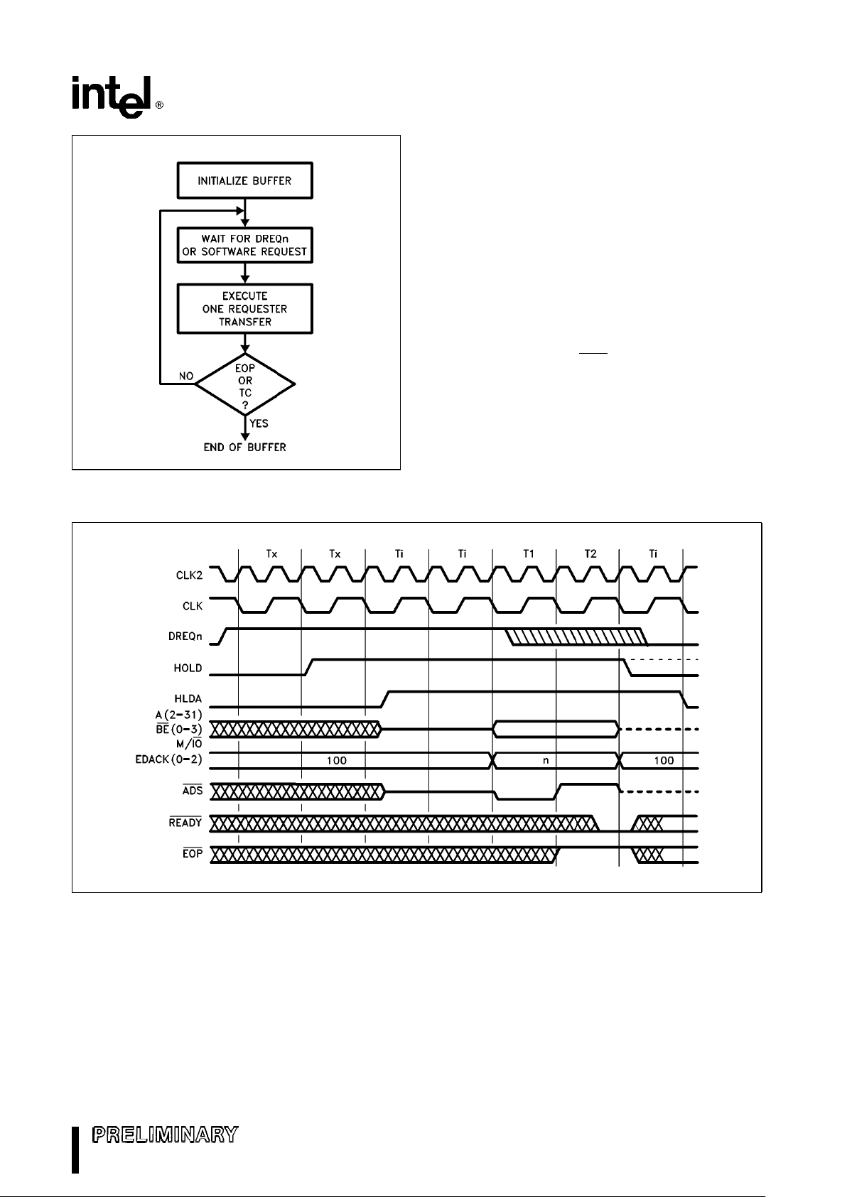
to the host between each transfer. Figure 17 shows
the logical flow of events which make up a buffer
transfer using the Single Transfer Mode.
26
Page 27
M82380
271070–18
Figure 17. Buffer Transfer in
Single Transfer Mode
The Single Transfer Mode is used for devices which
require complete handshake cycles with each data
access. Data is transferred to or from the Requester
only when the Requester is ready to perform the
transfer. Each transfer requires the entire DREQHOLD-HLDA-DACK handshake cycle. Figure 18
shows the timing of the Single Transfer Mode cycles.
BLOCK TRANSFER MODE
In the Block Transfer Mode, the DMA process is initiated by a DMA request and continues until the Byte
count expires, or until EOP
is activated by the Requester. The DREQn signal need only be held active
until the first Requester access. Only a refresh cycle
will interrupt the block transfer process.
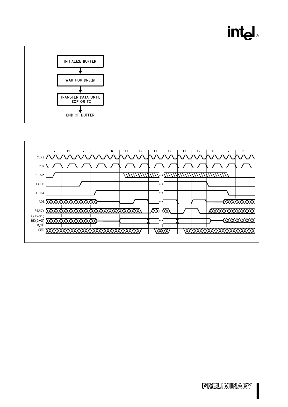
Figure 19 illustrates the operation of the DMA during
the Block Transfer Mode. Figure 20 shows the timing of the handshake signals during Block Mode
Transfers.
271070–19
Figure 18. DMA Single Transfer Mode
27
Page 28
M82380
271070–20
Figure 19. Buffer Transfer in
Block Transfer Mode
DEMAND TRANSFER MODE
The Demand Transfer Mode provides the most flexible handshaking procedures during the DMA process. A Demand Transfer is initiated by a DMA request. The process continues until the Byte Count
expires, or an external EOP
is encountered. If the
device being serviced (Requester) desires, it can interrupt the DMA process by de-activating the
DREQn line. Action is taken on the condition of
DREQn during Requester accesses only. The access during which DREQn is sampled inactive is the
last Requester access which will be performed during the current transfer. Figure 21 shows the flow of
events during the transfer of a buffer in the Demand
Mode.
271070–21
Figure 20. Block Mode Transfers
28
Page 29
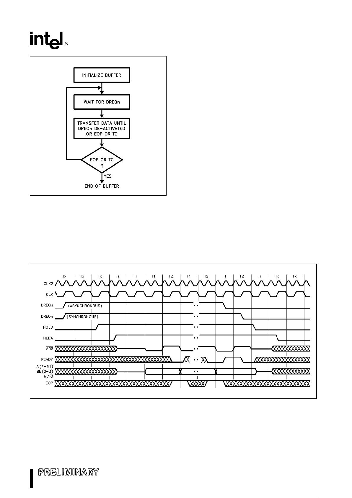
M82380
271070–22
Figure 21. Buffer Transfer in
Demand Transfer Mode
When the DREQn line goes inactive, the DMA controller will complete the current transfer, including
any necessary accesses to the Target, and relinquish control of the bus to the host. The current process information is saved (byte count, Requester
and Target addresses, and Temporary Register).
The Requester can restart the transfer process by
reasserting DREQn. The M82380 will arbitrate the
request with other pending requests and begin the
process where it left off. Figure 22 shows the timing
of handshake signals during Demand Transfer Mode
operation.
Using the Demand Transfer Mode allows peripherals
to access memory in small, irregular bursts without
wasting bus control time. The M82380 is designed to
give the best possible bus control latency in the Demand Transfer Mode. Bus control latency is defined
here as the time from the last active bus cycle of the
previous bus master to the first active bus cycle of
the new bus master. The M82380 DMA Controller
will perform its first bus access cycle two bus states
after HLDA goes active. In the typical configuration,
bus control is returned to the host one bus state
after the DREQn goes inactive.
There are two cases where there may be more than
one bus state of bus control latency at the end of a
transfer. The first is at the end of an Auto-Initialize
process, and the second is at the end of a process
where the source is the Requester and Two-Cycle
transfers are used.
When a Buffer Auto-Initialize Process is complete,
the M82380 requires seven bus states to reload the
271070–23
Figure 22. Demand Mode Transfers
29
Page 30
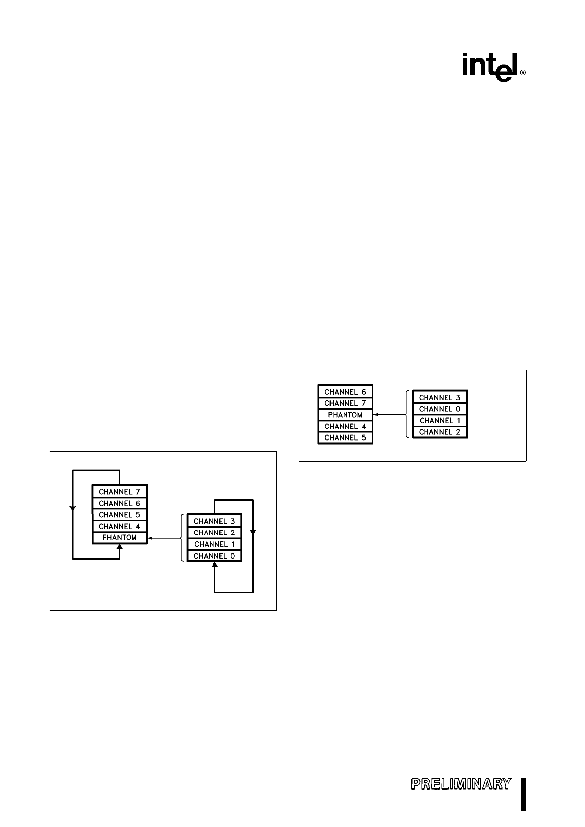
M82380
Current Registers from the Base Registers of the
Auto-Initialized channel. The reloading is done while
the M82380 is still the bus master so that it is prepared to service the channel immediately after relinquishing the bus, if necessary.
In the case where the Requester is the source, and
Two-Cycle transfers are being used, there are two
extra idle states at the end of the transfer process.
This occurs due to housekeeping in the DMA’s internal pipeline. These two idle states are present only
after the very last Requester access, before the
DMA Controller de-activates the HOLD signal.
3.3.4 CHANNEL PRIORITY ARBITRATION
DMA channel priority can be programmed into one
of two arbitration methods: Fixed or Rotating. The
four lower DMA channels and the four upper DMA
channels operate as if they were two separate DMA
controllers operating in cascade. The lower group of
four channels (0 – 3) is always prioritized between
channels 7 and 4 of the upper group of channels (4–
7). Figure 23 shows a pictorial representation of the
priority grouping.
The priority can thus be set up as rotating for one
group of channels and fixed for the other, or any
other combination. While in Fixed Priority, the programmer can also specify which channel has the
lowest priority.
271070–24
Figure 23. DMA Priority Grouping
The M82380 DMA Controller defaults to Fixed Priority. Channel 0 has the highest priority, then 1, 2, 3, 4,
5, 6, 7. Channel 7 has the lowest priority. Any time
the DMA Controller arbitrates DMA requests, the requesting channel with the highest priority will be
serviced next.
Fixed Priority can be entered into at any time by a
software command. The priority levels in effect
after the mode switch are determined by the current
setting of the Programmable Priority.
Programmable Priority is available for fixing the priority of the DMA channels within a group to levels other than the default. Through a software command,
the channel to have the lowest priority in a group
can be specified. Each of the two groups of four
channels can have the priority fixed in this way. The
other channels in the group will follow the natural
Fixed Priority sequence. This mode affects only the
priority levels while operating with Fixed Priority.
For example, if channel 2 is programmed to have the
lowest priority in its group, channel 3 has the highest
priority. In descending order, the other channels
would have the following priority: (3, 0, 1, 2), 4, 5, 6,
7 (channel 2 lowest, channel 3 highest). If the upper
group were programmed to have channel 5 as the
lowest priority channel, the priority would be (again,
highest to lowest): 6, 7, (3, 0, 1, 2), 4, 5. Figure 24
shows this example pictorially. The lower group is
always prioritized as a fifth channel of the upper
group (between channels 4 and 7).
High Priority
Low Priority
271070–25
Figure 24. Example of Programmed Priority
The DMA Controller will only accept Programmable
Priority commands while the addressed group is operating in Fixed Priority. Switching from Fixed to Rotating Priority preserves the current priority levels.
Switching from Rotating to Fixed Priority returns the
priority levels to those which were last programmed
by use of Programmable Priority.
Rotating Priority allows the devices using DMA to
share the system bus more evenly. An individual
channel does not retain highest priority after being
serviced, priority is passed to the next highest priority channel in the group. The channel which was
most recently serviced inherits the lowest priority.
This rotation occurs each time a channel is serviced.
Figure 25 shows the sequence of events as priority
is passed between channels. Note that the lower
group rotates within the upper group, and that servicing a channel within the lower group causes rotation within the group as well as rotation of the upper
group.
30
Page 31
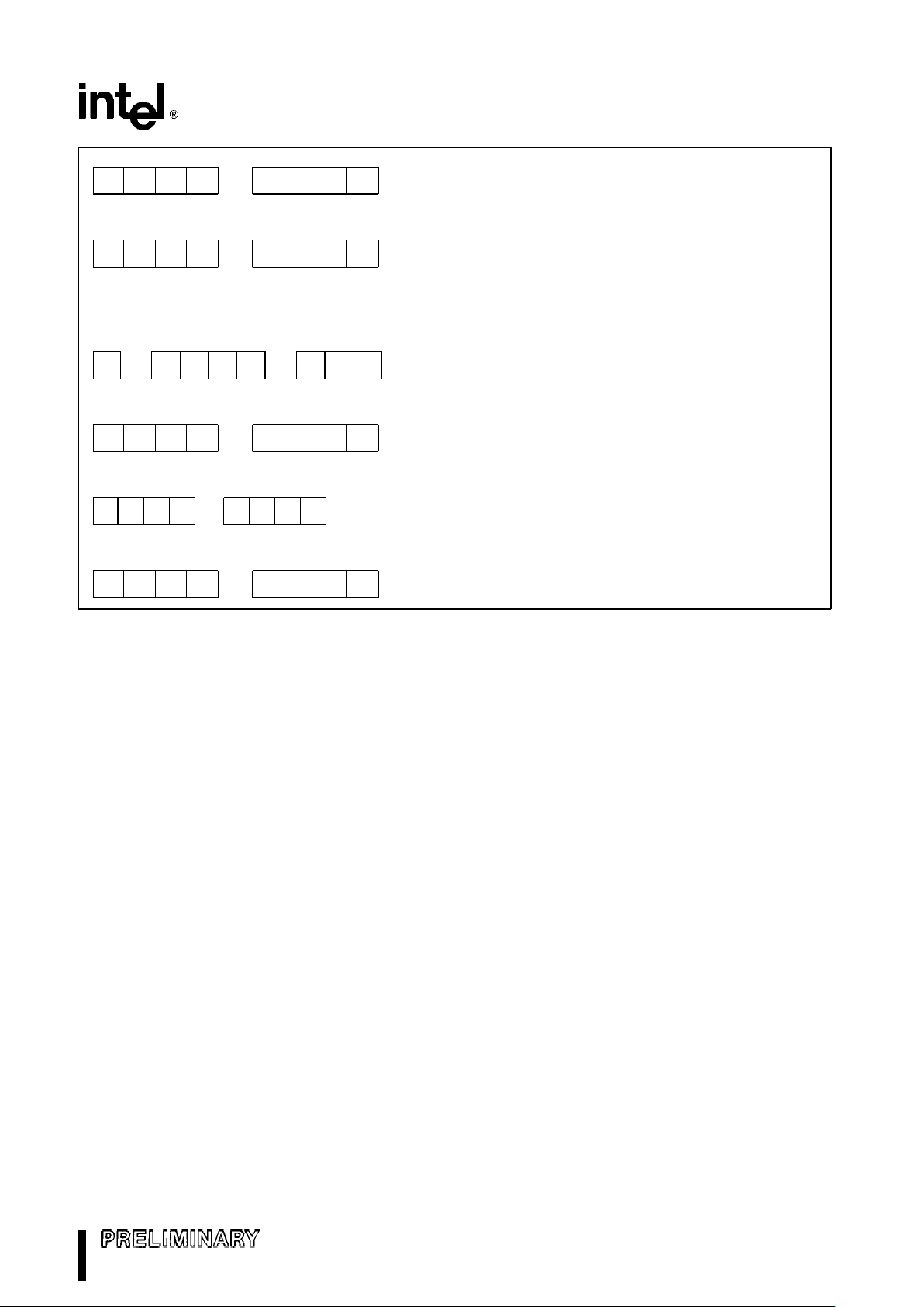
M82380
0123 4567Ðdefault (highest to lowest)
DREQ2 and DREQ6Ðprocess channel 2
4567 3012Ðchannel 2 drops to lowest priority within group.
Lower group drops to lowest priority within upper group.
2(Double Rotation)
DREQ6 (still) and DREQ7Ðprocess channel 6
7 3 0 1 2 4 5 6 Ðchannel 6 drops to lowest priority within group
DREQ7 (still) and DREQ0Ðprocess channel 7
3012 4567Ðchannel 7 drops to lowest priority within group
DREQ0 (still) and DREQ1Ðprocess channel 0
4567 1230Ðchannel 0 drops to lowest priority within group (Double Rotation)
DREQ1 (still)Ðprocess channel 1
4567 2301Ðchannel 1 drops to lowest priority within group
Figure 25. Rotating Channel Priority.
Lower and Upper groups are programmed for the Rotating Priority Mode.
31
Page 32
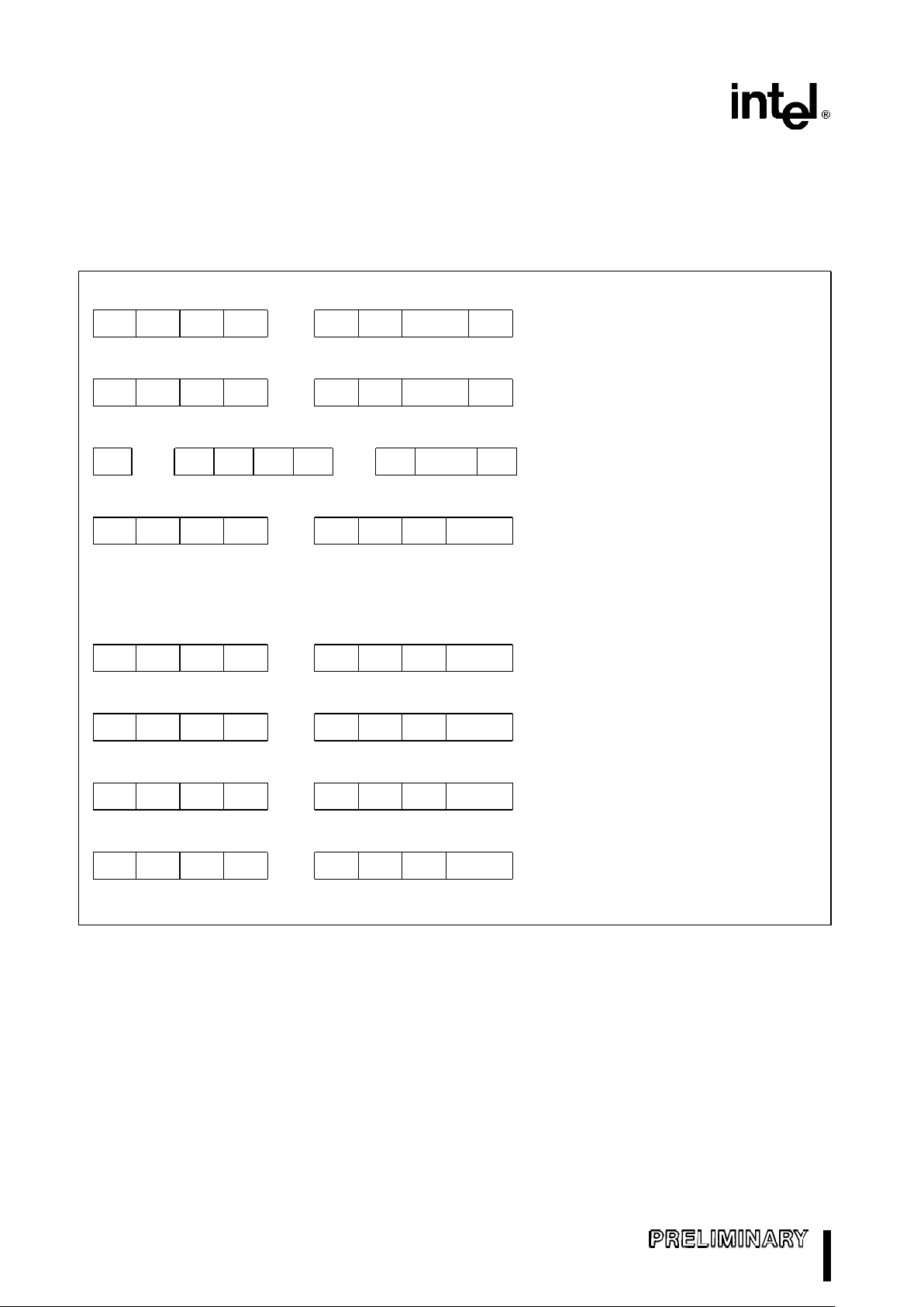
M82380
3.3.5 COMBINING PRIORITY MODES
Since the DMA Controller operates as two fourchannel controllers in cascade, the overall priority
scheme of all eight channels can take on a variety of
forms. There are four possible combinations of prior-
ity modes between the two groups of channels:
Fixed Priority only (default), Fixed Priority upper
group/Rotating Priority lower group, Rotating Priority
upper group/Fixed Priority lower group, and Rotating
Priority only. Figure 26 illustrates the operation of the
two combined priority methods.
High Low
0 1 2 3 4 5 6 7 ÐDefault priority
High Low
4 5 6 7 0 1 2 3 After servicing channel 2
High Low
7 0 1 2 3 4 5 6 ÐAfter servicing channel 6
High Low
4 5 6 7 0 1 2 3 ÐAfter servicing channel 1
CASE 1 0 –3 Fixed Priority, 4–7 Rotating Priority
High Low
0 1 2 3 4 5 6 7 Default priority
High Low
3 0 1 2 4 5 6 7 After servicing channel 2
High Low
3 0 1 2 4 5 6 7 After servicing channel 6
High Low
2 3 0 1 4 5 6 7 After servicing channel 1
CASE 2 0 –3 Rotating Priority, 4–7 Fixed Priority
Figure 26. Combining Priority Modes
32
Page 33

M82380
3.3.6 BUS OPERATION
Data may be transferred by the DMA Controller using two different bus cycle operations: Fly-By (onecycle) and Two-Cycle. These bus handshake methods are selectable independently for each channel
through a command register. Device data path
widths are independently programmable for both
Target and Requester. Also selectable through software is the direction of data transfer. All of these
parameters affect the operation of the M82380 on a
bus-cycle by bus-cycle basis.
FLY-BY TRANSFERS
The Fly-By Transfer Mode is the fastest and most
efficient way to use the M82380 DMA Controller to
transfer data. In this method of transfer, the data is
written to the destination device at the same time it
is read from the source. Only one bus cycle is used
to accomplish the transfer.
In the Fly-By Mode, the DMA acknowledge signal is
used to select the Requester. The DMA Controller
simultaneously places the address of the Target on
the address bus. The state of M/IO
and W/R during
the Fly-By transfer cycle indicate the type of Target
and whether the target is being written to or read
from. The Target’s Bus Size is used as an incrementer for the Byte Count. The Requester address registers are ignored during Fly-By transfers.
Note that memory-to-memory transfers cannot be
done using the Fly-By Mode. Only one memory or
I/O address is generated by the DMA Controller at a
time during Fly-By transfers. Only one of the devices
being accessed can be selected by an address.
Also, the Fly-By method of data transfer limits the
hardware to accesses of devices with the same data
bus width. The Temporary Registers are not affected in the Fly-By Mode.
Fly-By transfers also require that the data paths of
the Target and Requester be directly connected.
This requires that successive Fly-By accesses be to
doubleword boundaries, or that the Requester be
capable of switching its connections to the data bus.
TWO-CYCLE TRANSFERS
Two-Cycle transfers can also be performed by the
M82380 DMA Controller. These transfers require at
least two bus cycles to execute. The data being
transferred is read into the DMA Controller’s Temporary Register during the first bus cycle(s). The second bus cycle is used to write the data from the
Temporary Register to the destination.
If the addresses of the data being transferred are
not word or doubleword aligned, the M82380 will
recognize the situation and read and write the data
in groups of bytes, placing them always at the proper
destination. This process of collecting the desired
bytes and putting them together is called ‘byte assembly’. The reverse process (reading from aligned
locations and writing to non-aligned locations) is
called ‘byte disassembly’.
The assembly/disassembly process takes place
transparent to the software, but can only be done
while using the Two-Cycle transfer method. The
M82380 will always perform the assembly/disassembly process as necessary for the current data
transfer. Any data path widths for either the Requester or Target can be used in the Two-Cycle
Mode. This is very convenient for interfacing existing
8- and 16-bit peripherals to the i386 processor’s
32-bit bus.
The M82380 DMA Controller always attempts to fill
the Temporary Register from the source before writing any data to the destination. If the process is terminated before the Temporary Register is filled (TC
or EOP), the M82380 will write the partial data to the
destination. If a process is temporarily suspended
(such as when DREQn is de-activated during a demand transfer), the contents of a partially filled Temporary Register will be stored within the M82380 until the process is restarted.
For example, if the source is specified as an 8-bit
device and the destination as a 32-bit device, there
will be four reads as necessary from the 8-bit source
to fill the Temporary Register. Then the M82380 will
write the 32-bit contents to the destination. This cycle will repeat until the process is terminated or suspended.
Note that for a Single-Cycle transfer mode of operation, the internal circuitry of the DMA Controller actually executes single transfers by removing the DREQ
from the internal arbitration. Thus single transfers
from an 8-bit requester to a 32-bit target will consist
of four complete and independent 8-bit requester cycles, between which bus control is released and rerequested. Finally, the 32-bit data will be transferred
to the target device from the temporary register before the fifth requester cycle.
With Two-Cycle transfers, the devices that the
M82380 accesses can reside at any address within
I/O or memory space. The device must be able to
decode the byte-enables (BEn
). Also, if the device
cannot accept data in byte quantities, the programmer must take care not to allow the DMA Controller
to access the device on any address other than the
device boundary.
33
Page 34
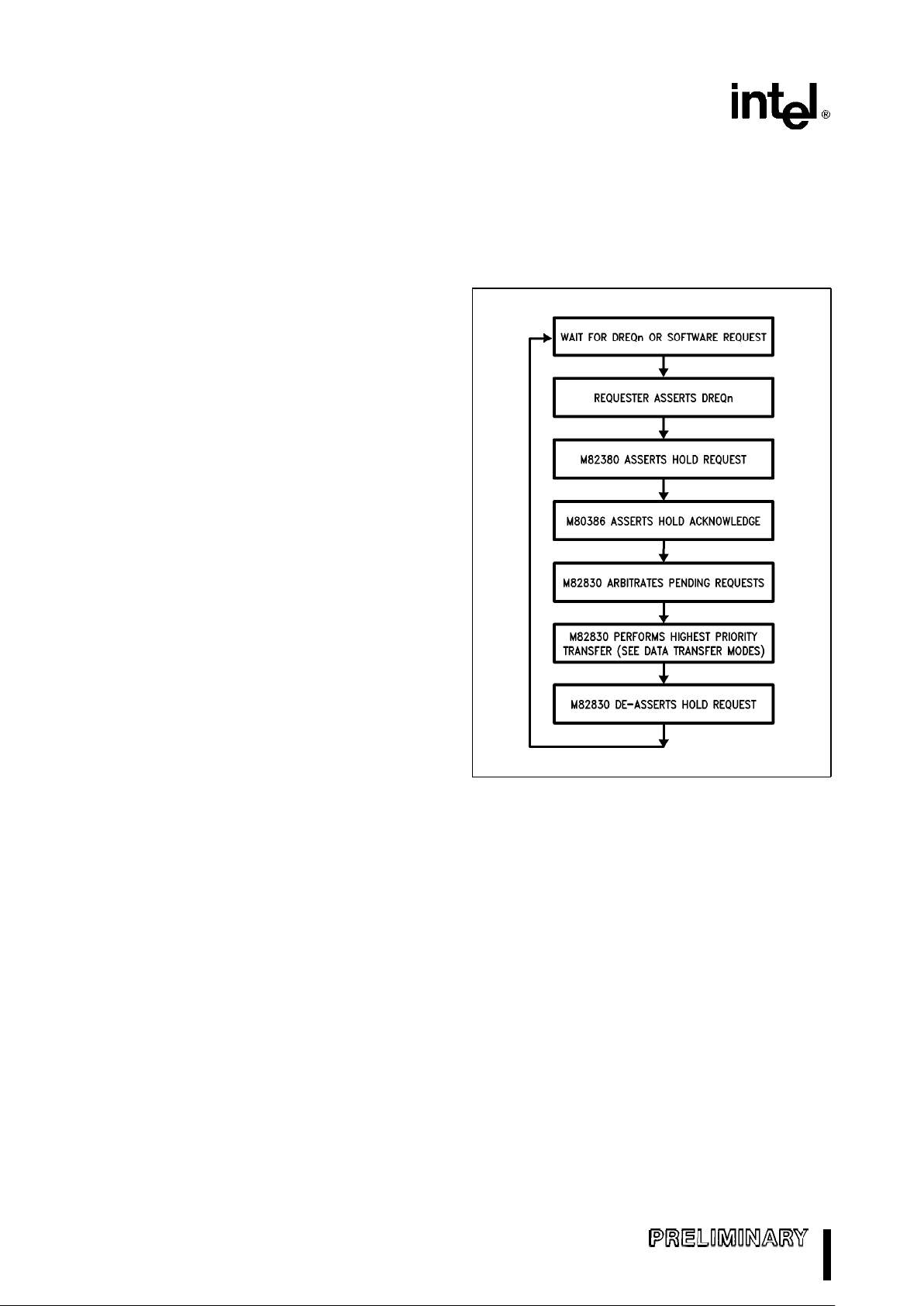
M82380
DATA PATH WIDTH AND DATA TRANSFER
RATE CONSIDERATIONS
The number of bus cycles used to transfer a single
‘word’ of data is affected by whether the Two-Cycle
or the Fly-By (Single-Cycle) transfer method is used.
The number of bus cycles used to transfer data directly affects the data transfer rate. Inefficient use of
bus cycles will decrease the effective data transfer
rate that can be obtained. Generally, the data transfer rate is halved by using Two-Cycle transfers instead of Fly-By transfers.
The choice of data path widths of both Target and
Requester affects the data transfer rate also. During
each bus cycle, the largest pieces of data possible
should be transferred.
The data path width of the devices to be accessed
must be programmed into the DMA controller. The
M82380 defaults after reset to 8-bit-to-8-bit data
transfers, but the Target and Requester can have
different data path widths, independent of each other and independent of the other channels. Since this
is a software programmable function, more discussion of the uses of this feature are found in the section on programming.
READ, WRITE, AND VERIFY CYCLES
Three different bus cycle types may be used in a
data transfer. They are the Read, Write, and Verify
cycles. These cycle types dictate the way in which
the M82380 operates on the data to be transferred.
A Read Cycle transfers data from the Target to the
Requester. A Write Cycle transfers data from the
Requester to the target. In a Fly-By transfer, the address and bus status signals indicate the access
(read or write) to the Target; the access to the Requester is assumed to be the opposite.
The Verify Cycle is used to perform a data read only.
No write access is indicated or assumed in a Verify
Cycle. The Verify Cycle is useful for validating block
fill operations. An external comparator must be provided to do any comparisons on the data read.
3.4 Bus Arbitration and Handshaking
Figure 27 shows the flow of events in the DMA request arbitration process. The arbitration sequence
starts when the Requester asserts a DREQn (or
DMA service is requested by software). Figure 28
shows the timing of the sequence of events following a DMA request. This sequence is executed for
each channel that is activated. The DREQn signal
can be replaced by a software DMA channel request
with no change in the sequence.
271070–26
Figure 27. Bus Arbitration and DMA Sequence
After the Requester asserts the service request, the
M82380 will request control of the bus via the HOLD
signal. The M82380 will always assert the HOLD signal one bus state after the service request is asserted. The i386 processor responds by asserting the
HLDA signal, thus releasing control of the bus to the
M82380 DMA Controller.
Priority of pending DMA service requests is arbitrated during the first state after HLDA is asserted by
the i386 processor. The next state will be the beginning of the first transfer access of the highest priority
process.
34
Page 35
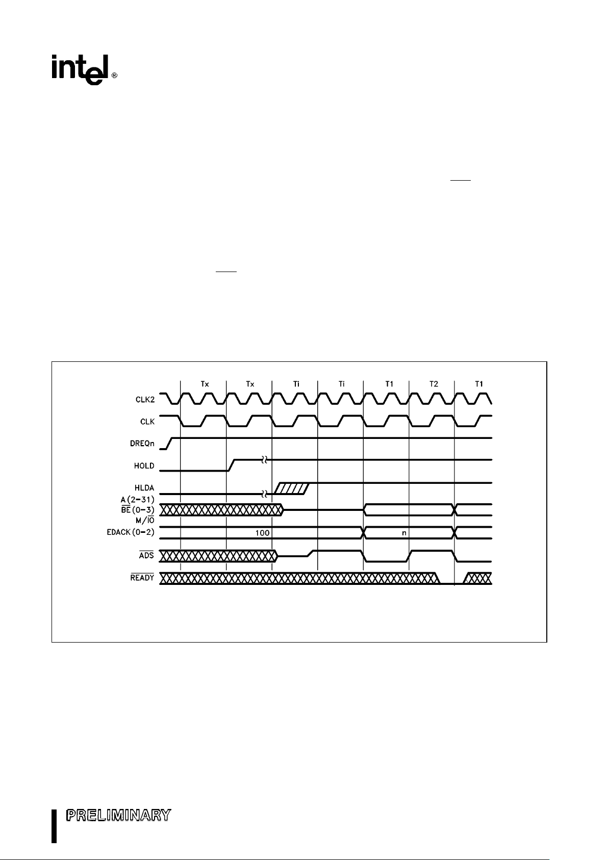
M82380
When the M82380 DMA Controller is finished with its
current bus activity, it returns control of the bus to
the host processor. This is done by driving the
HOLD signal inactive. The M82380 does not drive
any address or data bus signals after HOLD goes
low. It enters the Slave Mode until another DMA process is requested. The processor acknowledges
that it has regained control of the bus by forcing the
HLDA signal inactive. Note that the M82380’s DMA
Controller will not re-request control of the bus until
the entire HOLD/HLDA handshake sequence is
complete.
The M82380 DMA Controller will terminate a current
DMA process for one of three reasons: expired byte
count, end-of-process command (EOP
activated)
from a peripheral, or de-activated DMA request signal. In each case, the controller will de-assert HOLD
immediately after completing the data transfer in
progress. These three methods of process termination are illustrated in Figures 29, 32, and 31, respectively.
An expired byte count indicates that the current process is complete as programmed and the channel
has no further transfers to process. The channel
must be restarted according to the currently programmed Buffer Transfer Mode, or reprogrammed
completely, including a new Buffer Transfer Mode.
If the peripheral activates the EOP
signal, it is indicating that it will not accept or deliver any more data
for the current buffer. The M82380 DMA Controller
considers this as a completion of the channel’s current process and interprets the condition the same
way as if the byte count expired.
The action taken by the M82380 DMA Controller in
response to a de-activated DREQn signal depends
on the Data Transfer Mode of the channel. In the
Demand Mode, data transfers will take place as long
as the DREQn is active and the byte count has not
expired. In the Block Mode, the controller will complete the entire block transfer without relinquishing
271070–27
NOTE:
Channel priority resolution takes place during the bus state before HLDA is asserted, allowing the DMA Controller to
respond to HLDA without extra idle bus states.
Figure 28. Beginning of a DMA Process
35
Page 36

M82380
the bus, even if DREQn goes inactive before the
transfer is complete. In the Single Mode, the controller will execute single data transfers, relinquishing
the bus between each transfer, as long as DREQn is
active.
Normal termination of a DMA process due to expiration of the byte count (Terminal Count-TC) is shown
in Figure 29. The condition of DREQn is ignored until
after the process is terminated. If the channel is programmed to auto-initialize, HOLD will be held active
for an additional seven clock cycles while the autoinitialization takes place.
Table 6 shows the DMA channel activity due to EOP
or Byte Count expiring (Terminal Count).
Table 6. DMA Channel Activity Due to Terminal Count or External EOP
Single
Auto- Chaining-
Buffer Process: or Chaining-
Initialize Base Loaded
Base Empty
Event
Terminal Count True X True X True X
EOP
Input X 0 X 0 X 0
Results
Current Registers Ð Ð Load Load Load Load
Channel Mask Set Set ÐÐÐÐ
EOP Output 0 X 0 X 1 X
Terminal Count Status Set Set Set Set Ð Ð
Software Request CLR CLR CLR CLR Ð Ð
271070–28
Figure 29. Termination of a DMA Process Due to Expiration of Current Byte Count
36
Page 37

M82380
The M82380 always relinquishes control of the bus
between channel services. This allows the hardware
designer the flexibility to externally arbitrate bus hold
requests, if desired. If another DMA request is pending when a higher priority channel service is completed, the M82380 will relinquish the bus until the
hold acknowledge is inactive. One bus state after
the HLDA signal goes inactive, the M82380 will assert HOLD again. This is illustrated in Figure 30.
3.4.1 SYNCHRONOUS AND ASYNCHRONOUS
SAMPLING OF DREQn AND EOP
As an indicator that a DMA service is to be started,
DREQn is always sampled asynchronously. It is
sampled at the beginning of a bus state and acted
upon at the end of the state. Figure 28 illustrates the
start of a DMA process due to a DREQn input.
The DREQn and EOP
inputs can be programmed to
be sampled either synchronously or asynchronously
to signal the end of a transfer.
The synchronous mode affords the Requester one
bus state of extra time to react to an access. This
means the Requester can terminate a process on
the current access, without losing any data. The
asynchronous mode requires that the input signal be
presented prior to the beginning of the last state of
the Requester access.
The timing relationships of the DREQn and EOP
signals to the termination of a DMA transfer are shown
in Figures 31 and 32. Figure 31 shows the termination of a DMA transfer due to inactive DREQn. Figure 32 shows the termination of a DMA process due
to an active EOP
input.
In the Synchronous Mode, DREQn and EOP
are
sampled at the end of the last state of every Requester data transfer cycle. If EOP
is active or
DREQn is inactive at this time, the M82380 recognizes this access to the Requester as the last transfer. At this point, the M82380 completes the transfer
in progress, if necessary, and returns bus control to
the host.
In the asynchronous mode, the inputs are sampled
at the beginning of every state of a Requester access. The M82380 waits until the end of the state to
act on the input.
DREQn and EOP
are sampled at the latest possible
time when the M82380 can determine if another
transfer is required. In the Synchronous Mode,
DREQn and EOP
are sampled on the trailing edge of
the last bus state before another data access cycle
begins. The Asynchronous Mode requires that the
signals be valid one clock cycle earlier.
271070–29
Figure 30. Switching between Active DMA Channels
37
Page 38
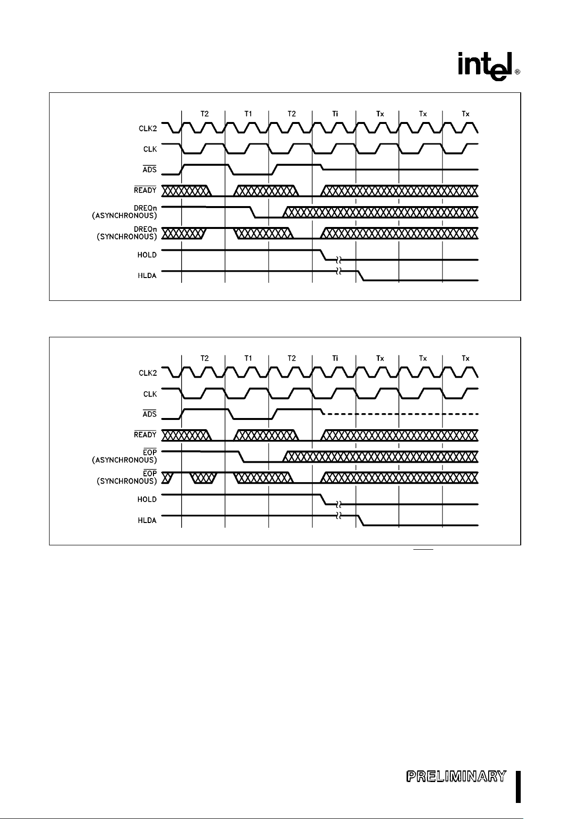
M82380
271070–30
Figure 31. Termination of a DMA Process Due to De-Asserting DREQn
271070–31
Figure 32. Termination of a DMA Process Due to an External EOP
38
Page 39

M82380
While in the Pipeline Mode, if the NA signal is sampled active during a transfer, the end of the state
where NA
was sampled active is when the M82380
decides whether to commit to another transfer. The
device must de-assert DREQn or assert EOP
before
NA
is asserted, otherwise the M82380 will commit to
another, possibly undesired, transfer.
Synchronous DREQn and EOP
sampling allows the
peripheral to prevent the next transfer from occurring by de-activating DREQn or asserting EOP
during the current Requester access, before the
M82380 DMA Controller commits itself to another
transfer. The DMA Controller will not perform the
next transfer if it has not already begun the bus cycle. Asynchronous sampling allows less stringent
timing requirements than the Synchronous Mode,
but requires that the DREQn signal be valid at the
beginning of the next to last bus state of the current
Requester access.
Using the Asynchronous Mode with zero wait states
can be very difficult. Since the addresses and control signals are driven by the M82380 near half-way
through the first bus state of a transfer, and the
Asynchronous Mode requires that DREQn be active
before the end of the state, the peripheral being accessed is required to present DREQn only a few
nanoseconds after the control information is available. This means that the peripheral’s control logic
must be extremely fast (practically non-causal). An
alternative is the Synchronous Mode.
3.4.2 ARBITRATION OF CASCADED MASTER
REQUESTS
The Cascade Mode allows another DMA-type device to share the bus by arbitrating its bus accesses
with the M82380’s. Seven of the eight DMA channels (0 –3 and 5– 7) can be connected to a cascaded
device. The cascaded device requests bus control
through the DREQn line of the channel which is programmed to operate in Cascade Mode. Bus hold acknowledge is signaled to the cascaded device
through the EDACK lines. When the EDACK lines
are active with the code for the requested cascade
channel, the bus is available to the cascaded master
device.
271070–32
Figure 33. Cascaded Bus Master
39
Page 40
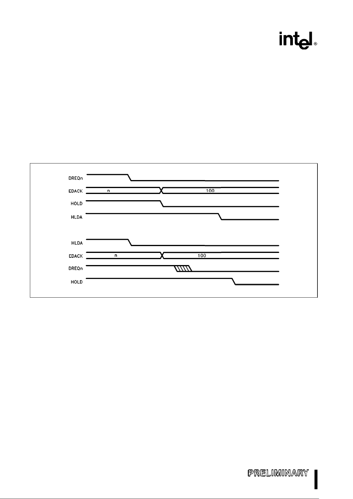
M82380
A Cascade cycle begins the same way a regular
DMA cycle begins. The requesting bus master asserts the DREQn line on the M82380. This bus control request arbitrated as any other DMA request
would be. If any channel receives a DMA request,
the M82380 requests control of the bus. When the
host acknowledges that it has released bus control,
the M82380 acknowledges to the requesting master
that it may access the bus. The M82380 enters an
idle state until the new master relinquishes control.
A cascade cycle will be terminated by one of two
events: DREQn going inactive, or HLDA going inactive. The normal way to terminate the cascade cycle
is for the cascaded master to drop the DREQn signal. Figure 34 shows the two cascade cycle termination sequences.
The Refresh Controller may interrupt the cascaded
master to perform a refresh cycle. If this occurs, the
M82380 DMA Controller will de-assert the EDACK
signal (hold acknowledge to cascaded master) and
wait for the cascaded master to remove its hold request. When the M82380 regains bus control, it will
perform the refresh cycle in its normal fashion. After
the refresh cycle has been completed, and if the
cascaded device has re-asserted its request, the
M82380 will return control to the cascaded master
which was interrupted.
271070–33
Cascade cycle termination by DREQn inactive
271070–34
Cascade cycle termination by HLDA inactive
Figure 34. Cascade Cycle Termination
40
Page 41

M82380
The M82380 assumes that it is the only device monitoring the HLDA signal. If the system designer
wishes to place other devices on the bus as bus
masters, the HLDA from the processor must be intercepted before presenting it to the M82380. Using
the Cascade capability of the M82380 DMA Controller offers a much better solution.
3.4.3 ARBITRATION OF REFRESH REQUESTS
The arbitration of refresh requests by the DRAM Refresh Controller is slightly different from normal DMA
channel request arbitration. The M82380 DRAM Refresh Controller always has the highest priority of
any DMA process. It also can interrupt a process in
progress. Two types of processes in progress may
be encountered: normal DMA, and bus master cascade.
In the event of a refresh request during a normal
DMA process, the DMA Controller will complete the
data transfer in progress and then execute the refresh cycle before continuing with the current DMA
process. The priority of the interrupted process is
not lost. If the data transfer cycle interrupted by the
Refresh Controller is the last of a DMA process, the
refresh cycle will always be executed before control
of the bus is transferred back to the host.
When the Refresh Controller request occurs during
a cascade cycle, the Refresh Controller must be assured that the cascaded master device has relinquished control of the bus before it can execute the
refresh cycle. To do this, the DMA Controller drops
the EDACK signal to the cascaded master and waits
for the corresponding DREQn input to go inactive.
By dropping the DREQn signal, the cascaded master relinquishes the bus. The Refresh Controller then
performs the refresh cycle. Control of the bus is returned to the cascaded master if DREQn returns to
an active state before the end of the refresh cycle,
otherwise control is passed to the processor and the
cascaded master loses its priority.
3.5 DMA Controller Register Overview
The M82380 DMA Controller contains 44 registers
which are accessable to the host processor. Twenty-four of these registers contain the device addresses and data counts for the individual DMA
channels (three per channel). The remaining registers are control and status registers for initiating and
monitoring the operation of the M82380 DMA Controller. Table 7 lists the DMA Controller’s registers
and their accessability.
Table 7. DMA Controller Registers
Register Name Access
Control/Status RegisterÐOne Each Per
Group
Command Register I Write Only
Command Register II Write Only
Mode Register I Write Only
Mode Register II Write Only
Software Request Register Read/Write
Mask Set-Reset Register Write Only
Mask Read-Write Register Read/Write
Status Register Read Only
Bus Size Register Write Only
Chaining Register Read/Write
Channel RegistersÐOne Each Per Channel
Base Target Address Write Only
Current Target Address Read Only
Base Requester Address Write Only
Current Requester Address Read Only
Base Byte Count Write Only
Current Byte Count Read Only
3.5.1 CONTROL/STATUS REGISTERS
The following registers are available to the host
processor for programming the M82380 DMA Controller into its various modes and for checking the
operating status of the DMA processes. Each set of
four DMA channels has one of each of these registers associated with it.
Command Register I
Enables or disables the DMA channels as a group.
Sets the Priority Mode (Fixed or Rotating) of the
group. This write-only register is cleared by a hardware reset, defaulting to all channels enabled and
Fixed Priority Mode.
Command Register II
Sets the sampling mode of the DREQn and EOP
inputs. Also sets the lowest priority channel for the
group in the Fixed Priority Mode. The functions programmed through Command Register II default after
a hardware reset to: asynchronous DREQn and
EOP, and channels 3 and 7 lowest priority.
Mode Register I
Mode Register I programs the following functions for
an individually selected channel:
41
Page 42

M82380
Type of TransferÐread, write, verify
AutoÐInitializeÐenable or disable
Target Address CountÐincrement or
decrement
Data Transfer ModeÐdemand, single, block,
cascade
Mode Register I functions default to the following
after reset: verify transfer, Auto-Initialize disabled, Increment Target address, Demand Mode.
Mode Register II
Programs the following functions for an individually
selected channel:
Target Address HoldÐenable or disable
Requester Address CountÐincrement
or decrement
Requester Address HoldÐenable or disable
Target Device TypeÐI/O or Memory
Requester Device TypeÐI/O or Memory
Transfer CyclesÐTwo-Cycle or Fly-By
Mode Register II functions are defined as follows
after a hardware reset: Disable Target Address Hold,
Increment Requester Address, Target (and Requester) in memory, Fly-By Transfer Cycles. Note:
Requester Device Type ignored in Fly-By Transfers.
Software Request Register
The DMA Controller can respond to service requests
which are initiated by software. Each channel has an
internal request status bit associated with it. The
host processor can write to this register to set or
reset the request bit of a selected channel.
The status of the group’s software DMA service requests can be read from this register as well. Each
request bit is cleared upon Terminal Count or external EOP
.
The software DMA requests are non-maskable and
subject to priority arbitration with all other software
and hardware requests. The entire register is
cleared by a hardware reset.
Mask Registers
Each channel has associated with it a mask bit
which can be set/reset to disable/enable that channel. Two methods are available for setting and clearing the mask bits. The Mask Set/Reset Register is a
write-only register which allows the host to select an
individual channel and either set or reset the mask
bit for that channel only. The Mask Read/Write Register is available for reading the mask bit status and
for writing mask bits in groups of four.
The mask bits of a group may be cleared in one step
by executing the Clear Mask Command. See the
DMA Programming section for details. A hardware
reset sets all of the channel mask bits, disabling all
channels.
Status Register
The Status register is a read-only register which contains the Terminal Count (TC) and Service Request
status for a group. Four bits indicate the TC status
and four bits indicate the hardware request status
for the four channels in the group. The TC bits are
set when the Byte Count expires, or when an external EOP
is asserted. These bits are cleared by reading from the Status Register. The Service Request
bit for a channel indicates when there is a hardware
DMA request (DREQn) asserted for that channel.
When the request has been removed, the bit is
cleared.
Bus Size Register
This write-only register is used to define the bus size
of the Target and Requester of a selected channel.
The bus sizes programmed will be used to dictate
the sizes of the data paths accessed when the DMA
channel is active. The values programmed into this
register affect the operation of the Temporary Register. Any byte-assembly required to make the transfers using the specified data path widths will be done
in the Temporary Register. The Bus Size register of
the Target is used as an increment/decrement value
for the Byte Counter and Target Address when in
the Fly-By Mode. Upon reset, all channels default to
8-bit Targets and 8-bit Requesters.
Chaining Register
As a command or write register, the Chaining register is used to enable or disable the Chaining Mode
for a selected channel. Chaining can either be disabled or enabled for an individual channel, independently of the Chaining Mode status of other channels. After a hardware reset, all channels default to
Chaining disabled.
When read by the host, the Chaining Register provides the status of the Chaining Interrupt of each of
the channels. These interrupt status bits are cleared
when the new buffer information has been loaded.
3.5.2 CHANNEL REGISTERS
Each channel has three individually programmable
registers necessary for the DMA process; they are
the Base Byte Count, Base Target Address, and
Base Requester Address registers. The 24-bit Base
42
Page 43

M82380
Byte Count register contains the number of bytes to
be transferred by the channel. The 32-bit Base Target Address Register contains the beginning address (memory or I/O) of the Target device. The 32bit Base Requester Address register contains the
base address (memory or I/O) of the device which is
to request DMA service.
Three more registers for each DMA channel exist
within the DMA Controller which are directly related
to the registers mentioned above. These registers
contain the current status of the DMA process. They
are the Current Byte Count register, the Current Target Address, and the Current Requester Address. It
is these registers which are manipulated (incremented, decremented, or held constant) by the M82380
DMA Controller during the DMA process. The Current registers are loaded from the Base registers.
The Base registers are loaded when the host processor writes to the respective channel register addresses. Depending on the mode in which the channel is operating, the Current registers are typically
loaded in the same operation. Reading from the
channel register addresses yields the contents of
the corresponding Current register.
To maintain compatibility with software which accesses an 8237A, a Byte Pointer Flip-Flop is used to
control access to the upper and lower bytes of some
words of the Channel Registers. These words are
accessed as byte pairs at single port addresses. The
Byte Pointer Flip-Flop acts as a one-bit pointer
which is toggled each time a qualifying Channel
Register byte is accessed. It always points to the
next logical byte to be accessed of a pair of bytes.
The Channel registers are arranged as pairs of
words, each pair with its own port address. Addressing the port with the Byte Pointer Flip-Flop reset accesses the least significant byte of the pair. The
most significant byte is accessed when the Byte
Pointer is set.
For compatibility with existing 8237A designs, there
is one exception to the above statements about the
Byte Pointer Flip-Flop. The third byte (bits 16– 23) of
the Target Address is accessed through its own port
address. The Byte Pointer Flip-Flop is not affected
by any accesses to this byte.
The upper eight bits of the Byte Count Register are
cleared when the least significant byte of the register is loaded. This provides compatibility with software which accesses an 8237A. The 8237A has
16-bit Byte Count Registers.
3.5.3 TEMPORARY REGISTERS
Each channel has a 32-bit Temporary Register used
for temporary data storage during two-cycle DMA
transfers. It is this register in which any necessary
byte assembly and disassembly of non-aligned data
is performed. Figure 35 shows how a block of data
will be moved between memory locations with different boundaries. Note that the order of the data does
not change.
SOURCE DESTINATION
20H A 50H
21H B 51H
22H C 52H
23H D 53H A
24H E 54H B
25H F 55H C
26H G 56H D
27H 57H E
58H F
59H G
5AH
Targetesourcee00000020H
Requester
e
destinatione00000053H
Byte Count
e
000006H
Figure 35. Transfer of Data between Memory
Locations with Different Boundaries. This will be
the result, independent of data path width.
If the destination is the Requester and an early process termination has been indicated by the EOP
signal or DREQn inactive in the Demand Mode, the
Temporary Register is not affected. If data remains
in the Temporary Register due to differences in data
path widths of the Target and Requester, it will not
be transferred or otherwise lost, but will be stored for
later transfer.
If the destination is the Target and the EOP
signal is
sensed active during the Requester access of a
transfer, the DMA Controller will complete the transfer by sending to the Target whatever information is
in the Temporary Register at the time of process
termination. This implies that the Target could be
accessed with partial data. For this reason it is advisable to have an I/O device designated as a Requester, unless it is capable of handling partial data
transfers.
43
Page 44

M82380
3.6 DMA Controller Programming
Programming a DMA Channel to perform a needed
DMA function is in general a four step process. First
the global attributes of the DMA Controller are programmed via the two Command Registers. These
global attributes include: priority levels, channel
group enables, priority mode, and DREQn/EOP
in-
put sampling.
The second step involves setting the operating
modes of the particular channel. The Mode Registers are used to define the type of transfer and the
handshaking modes. The Bus Size Register and
Chaining Register may also need to be programmed
in this step.
The third step is setting up the channel is to load the
Base Registers in accordance with the needs of the
operating modes chosen in step two. The Current
Registers are automatically loaded from the Base
Registers, if required by the Buffer Transfer Mode in
effect. The information loaded and the order in
which it is loaded depends on the operating mode. A
channel used for cascading, for example, needs no
buffer information and this step can be skipped entirely.
The last step is to enable the newly programmed
channel using one of the Mask Registers. The channel is then available to perform the desired data
transfer. The status of the channel can be observed
at any time through the Status Register, Mask Register, Chaining Register, and Software Request register.
Once the channel is programmed and enabled, the
DMA process may be initiated in one of two ways,
either by a hardware DMA request (DREQn) or a
software request (Software Request Register).
Once programmed to a particular Process/Mode
configuration, the channel will operate in that configuration until programmed otherwise. For this reason,
restarting a channel after the current buffer expires
does not require complete reprogramming of the
channel. Only those parameters which have
changed need to be reprogrammed. The Byte Count
Register is always changed and must be reprogrammed. A Target or Requester Address Register
which is incremented or decremented should be reprogrammed also.
3.6.1 BUFFER PROCESSES
The Buffer Process is determined by the Auto-Initialize bit of Mode Register I and the Chaining Register.
If Auto-Initialize is enabled, Chaining should not be
used.
SINGLE BUFFER PROCESS
The Single Buffer Process is programmed by disabling Chaining via the Chaining Register and programming Mode Register I for non-Auto-Initialize.
BUFFER AUTO-INITIALIZE PROCESS
Setting the Auto-Initialize bit in Mode Register I is all
that is necessary to place the channel in this mode.
Buffer Auto-Initialize must not be enabled simultaneous to enabling the Buffer Chaining Mode as this
will have unpredictable results.
Once the Base Registers are loaded, the channel is
ready to be enabled. The channel will reload its Current Registers from the Base Registers each time
the Current Buffer expires, either by an expired Byte
Count or an external EOP
.
BUFFER CHAINING PROCESS
The Buffer Chaining Process is entered into from the
Single Buffer Process. The Mode Registers should
be programmed first, with all of the Transfer Modes
defined as if the channel were to operate in the Single Buffer Process. The channel’s Base and Current
Registers are then loaded. When the channel has
been set up in this way, and the chaining interrupt
service routine is in place, the Chaining Process can
be entered by programming the Chaining Register.
Figure 36 illustrates the Buffer Chaining Process.
44
Page 45
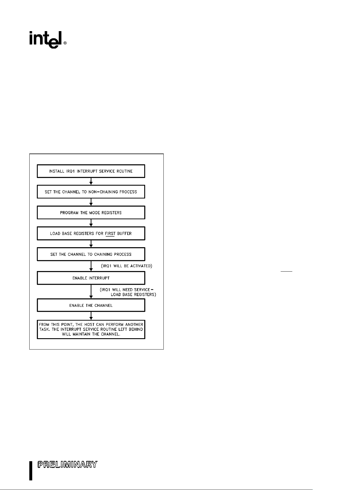
M82380
An interrupt (IRQ1) will be generated immediately after the Chaining Process is entered, as the channel
then perceives the Base Registers as empty and in
need of reloading. It is important to have the interrupt service routine in place at the time the Chaining
Process is entered into. The interrupt request is removed when the most significant byte of the Base
Target Address is loaded.
The interrupt will occur again when the first buffer
expires and the Current Registers are loaded from
the Base Registers. The cycle continues until the
Chaining Process is disabled, or the host fails to respond to IRQ1 before the Current Buffer expires.
271070–35
Figure 36. Flow of Events in the
Buffer Chaining Process
Exiting the Chaining Process can be done by resetting the Chaining Mode Register. If an interrupt is
pending for the channel when the Chaining Register
is reset, the interrupt request will be removed. The
Chaining Process can be temporarily disabled by
setting the channel’s Mask bit in the Mask Register.
The interrupt service routine for IRQ1 has the responsibility of reloading the Base Register as necessary. It should check the status of the channel to
determine the cause of channel expiration, etc. It
should also have access to operating system information regarding the channel, if any exists. The
IRQ1 service routine should be capable of determining whether the chain should be continued or terminated and act on that information.
3.6.2 DATA TRANSFER MODES
The Data Transfer Modes are selected via Mode
Register I. The Demand, Single, and Block Modes
are selected by bits D6 and D7. The individual transfer type (Fly-By vs Two-Cycle, Read-Write-Verify,
and I/O vs Memory) is programmed through both of
the Mode registers.
3.6.3 CASCADED BUS MASTERS
The Cascade Mode is set by writing ones to D7 and
D6 of Mode Register I. When a channel is programmed to operate in the Cascade Mode, all of the
other modes associated with Mode Registers I and II
are ignored. The priority and DREQn/EOP
definitions of the Command Registers will have the same
effect on the channel’s operation as any other
mode.
3.6.4 SOFTWARE COMMANDS
There are five port addresses which, when written
to, command certain operations to be performed by
the M82380 DMA Controller. The data written to
these locations is not of consequence, writing to the
location is all that is necessary to command the
M82380 to perform the indicated function. Following
are descriptions of the command function.
45
Page 46

M82380
Clear Byte Pointer Flip-FlopÐlocation 000CH
Resets the Byte Pointer Flip-Flop. This command
should be performed at the beginning of any access
to the channel registers in order to be assured of
beginning at a predictable place in the register programming sequence.
Master ClearÐlocation 000DH
All DMA functions are set to their default states. This
command is the equivalent of a hardware reset to
the DMA Controller. Functions other than those in
the DMA Controller section of the M82380 are not
affected by this command.
Clear Mask
Register ÐChannels 0–3Ðlocation 000EH
Channels 4 –7Ðlocation 00CEH
This command simultaneously clears the Mask Bits
of all channels in the addressed group, enabling all
of the channels in the group.
Clear TC Interrupt RequestÐlocation 001EH
This command resets the Terminal Count Interrupt
Request Flip-Flop. It is provided to allow the program which made a software DMA request to acknowledge that it has responded to the expiration of
the requested channel(s).
3.7 Register Definitions
The following diagrams outline the bit definitions and
functions of the M82380 DMA Controller’s Status
and Control Registers. The function and programming of the registers is covered in the previous section on DMA Controller Programming. An entry of ‘X’
as a bit value indicates ‘‘don’t care.’’
Channel Registers
(Read Current, Write Base)
Channel
Register Name Address Byte Bits
(Hex) Pointer Accessed
Channel 0 Target Address 00 0 0– 7
1 8–15
87 x 16–23
10 0 24–31
Byte Count 01 0 0– 7
1 8–15
11 0 16–23
Requester Address 90 0 0-7
1 8–15
91 0 16–23
1 24–31
Channel 1 Target Address 02 0 0– 7
1 8–15
83 x 16–23
12 0 24–31
Byte Count 03 0 0– 7
1 8–15
13 0 16–23
Requester Address 92 0 0-7
1 8–15
93 0 16–23
1 24–31
46
Page 47

M82380
Channel Registers
(Read Current, Write Base)
Channel
Register Name Address Byte Bits
(Hex) Pointer Accessed
Channel 2 Target Address 04 0 0– 7
1 8–15
81 x 16–23
14 0 24–31
Byte Count 05 0 0– 7
1 8–15
15 0 16–23
Requester Address 94 0 0-7
1 8–15
95 0 16–23
1 24–31
Channel 3 Target Address 06 0 0– 7
1 8–15
82 x 16–23
16 0 24–31
Byte Count 07 0 0– 7
1 8–15
17 0 16–23
Requester Address 96 0 0-7
1 8–15
97 0 16–23
1 24–31
Channel 4 Target Address C0 0 0 – 7
1 8–15
8F x 16–23
D0 0 24–31
Byte Count C1 0 0– 7
1 8–15
D1 0 16–23
Requester Address 98 0 0-7
1 8–15
99 0 16–23
1 24–31
Channel 5 Target Address C2 0 0 – 7
1 8–15
8B x 16–23
D2 0 24–31
Byte Count C3 0 0– 7
1 8–15
D3 0 16–23
Requester Address 9A 0 0-7
1 8–15
9B 0 16–23
1 24–31
47
Page 48
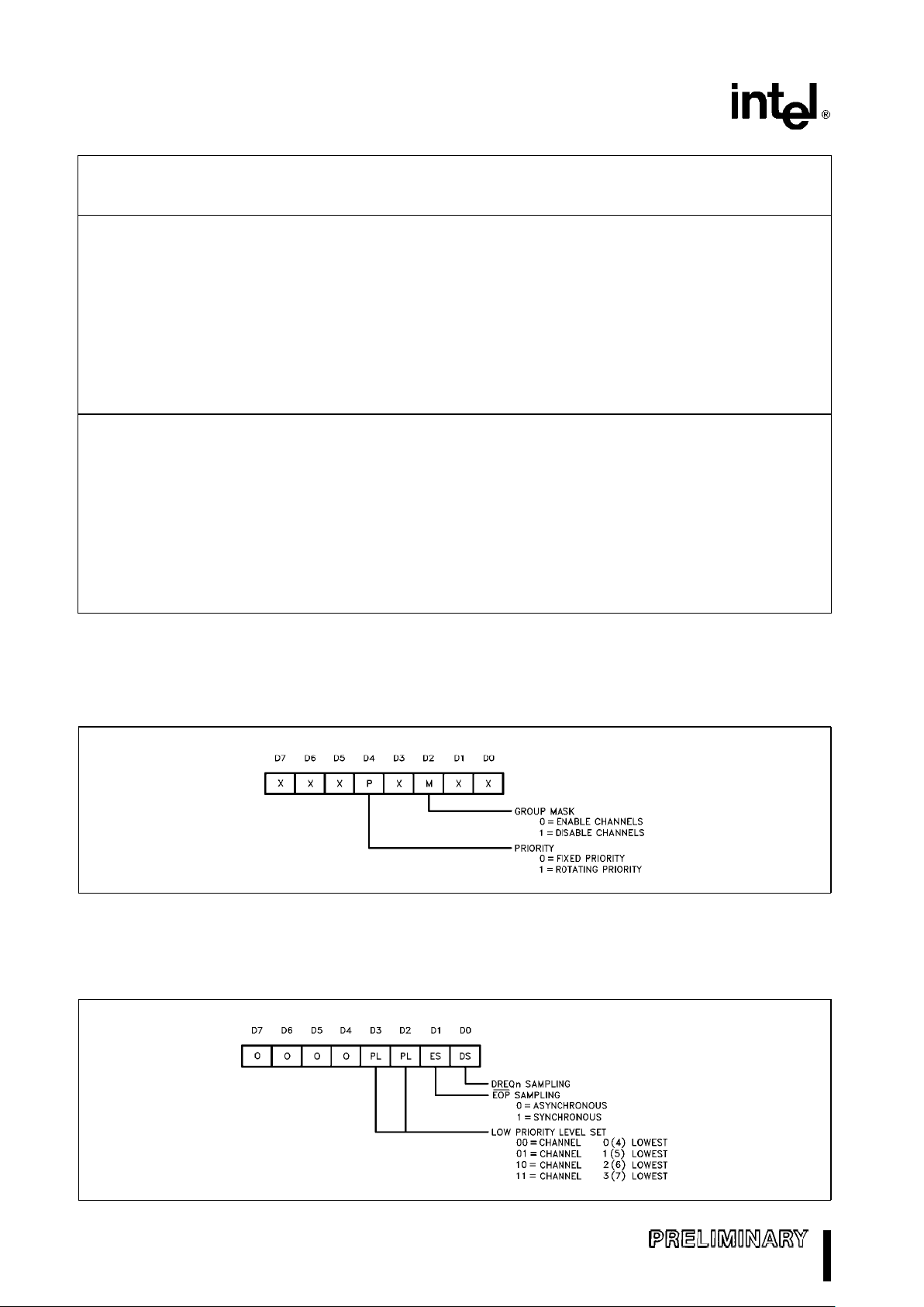
M82380
Channel Registers
(Read Current, Write Base)
Channel
Register Name Address Byte Bits
(Hex) Pointer Accessed
Channel 6 Target Address C4 0 0 – 7
1 8–15
89 x 16–23
D4 0 24–31
Byte Count C5 0 0– 7
1 8–15
D5 0 16–23
Requester Address 9C 0 0-7
1 8–15
9D 0 16–23
1 24–31
Channel 7 Target Address C6 0 0 – 7
1 8–15
8A x 16–23
D6 0 24–31
Byte Count C7 0 0– 7
1 8–15
D7 0 16–23
Requester Address 9E 0 0-7
1 8–15
9F 0 16–23
1 24–31
Command Register I (Write Only)
Port AddressÐChannels 0 – 3Ð0008H
Channels 4– 7Ð00C8H
271070–36
Command Register II (Write Only)
Port AddressesÐChannels 0 – 3Ð-001AH
Channels 4– 7Ð00DAH
271070–37
48
Page 49

M82380
Mode Register I (Write Only)
Port AddressesÐChannels 0 – 3Ð000BH
Channels 4– 7Ð00CBH
271070–38
* Target and Requester DECREMENT is allowed only for byte transfers.
Mode Register II (Write Only)
Port AddressesÐChannels 0 – 3Ð001BH
Channels 4– 7Ð00DBH
271070–39
* Target and Requester DECREMENT is allowed only for byte transfers.
49
Page 50
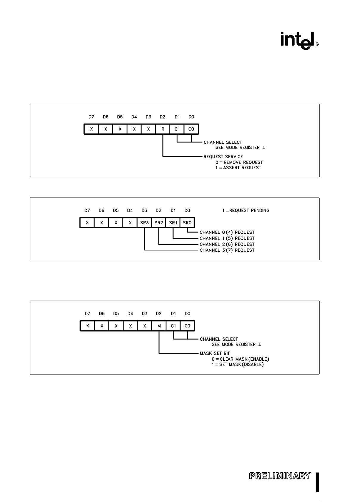
M82380
Software Request Register (Read/Write)
Port AddressesÐChannels 0 – 3Ð0009H
Channels 4– 7Ð00C9H
Write Format: Software DMA Service Request
271070–40
Read Format: Software Requests Pending
271070–41
Mask Set/Reset Register Individual Channel Mask (Write Only)
Port AddressesÐChannels 0 – 3Ð000AH
Channels 4– 7Ð00CAH
271070–42
50
Page 51
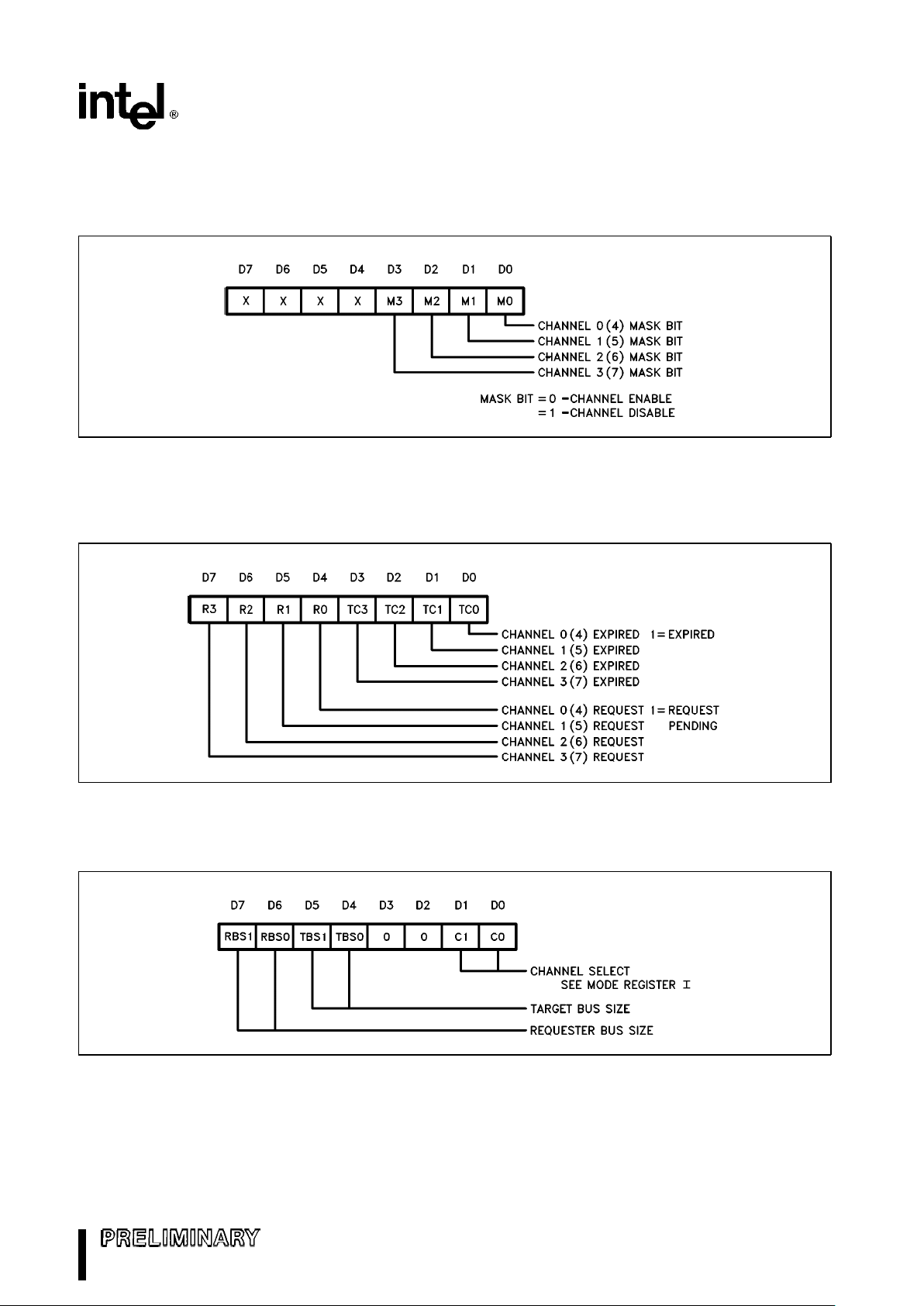
M82380
Mask Read/Write Register Group Channel Mask (Read/Write)
Port AddressesÐChannels 0 – 3Ð000FH
Channels 4– 7Ð00CFH
271070–43
Status Register Channel Process Status (Read Only)
Port AddressesÐChannels 0 – 3Ð0008H
Channels 4– 7Ð00C8H
271070–44
Bus Size Register Set Data Path Width (Write Only)
Port AddressesÐChannels 0 – 3Ð0018H
Channels 4– 7Ð00D8H
271070–45
Bus Size Encoding:
00
e
Reserved by Intel 10e16-bit Bus
01
e
32-bit Bus 11e8-bit Bus
51
Page 52

M82380
Chaining Register (Read/Write)
Port AddressesÐChannels 0 – 3Ð0019H
Channels 4– 7Ð00D9H
Write Format: Set Chaining Mode
271070–46
Read Format: Channel Interrupt Status
271070–47
52
Page 53
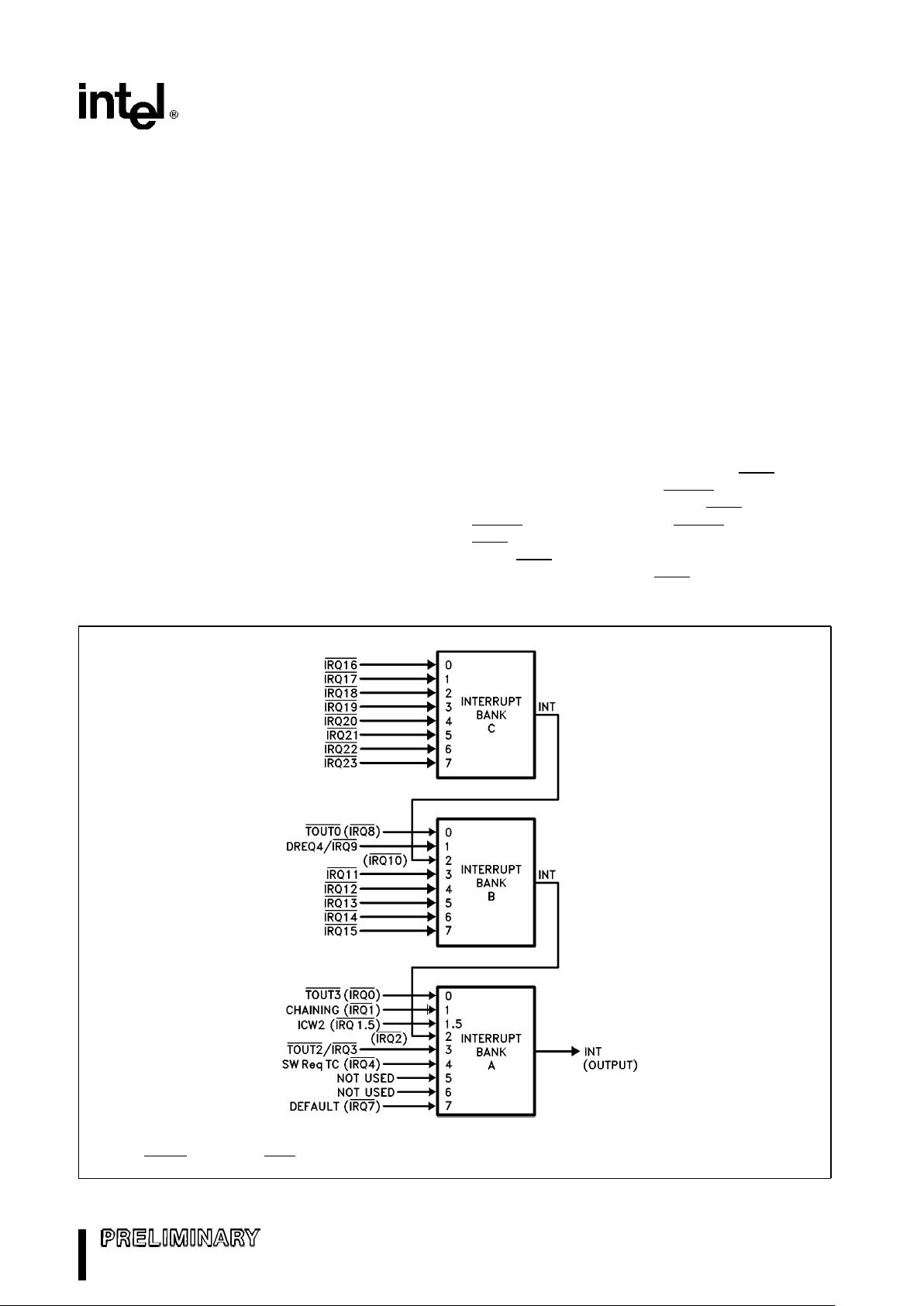
M82380
4.0 PROGRAMMABLE INTERRUPT
CONTROLLER
4.1 Functional Description
The M82380 Programmable Interrupt Controller
(PIC) consists of three enhanced M8259A Interrupt
Contollers. These three controllers together provide
15 external and 5 internal interrupt request inputs.
Each external request input can be cascaded with
an additional M8259A slave collector. This scheme
allows the M82380 to support a maximum of 120
(15 x 8) external interrupt request inputs.
Following one or more interrupt requests, the
M82380 PIC issues an interrupt signal to the i386
processor. When the i386 host processor responds
with an interrupt acknowledge signal, the PIC will arbitrate between the pending interrupt requests and
place the interrupt vector associated with the highest priority pending request on the data bus.
The major enhancement in the M82380 PIC over the
M8259A is that each of the interrupt request inputs
can be individually programmed with its own interrupt vector, allowing more flexibility in interrupt vector mapping.
4.1.1 INTERNAL BLOCK DIAGRAM
The block diagram of the M82380 Programmable Interrupt Controller is shown in Figure 37. Internally,
the PIC consists of three M8259A banks: A, B and
C. The three banks are cascaded to one another: C
is cascaded to B, B is cascaded to A. The INT output
of Bank A is used externally to interrupt the i386
processor.
Bank A has nine interrupt request inputs (two are
unused), and Banks B and C have eight interrupt
request inputs. Of the fifteen external interrupt request inputs, two are shared by other functions. Specifically, the Interrupt Request 3 input (IRQ3
) can be
used as the Timer 2 output (TOUT2
). This pin can be
used in three different ways: IRQ3
input only,
TOUT2
output only, or using TOUT2 to generate an
IRQ3
interrupt request. Also, the Interrupt Request 9
input (IRQ9
) can be used as DMA Request 4 input
(DREQ4). Typically, only IRQ9
or DREQ4 can be
used at a time.
271070–48
NOTE:
Masking IRQ1.5
also masks IRQ2.
Figure 37. Interrupt Controller Block Diagram
53
Page 54
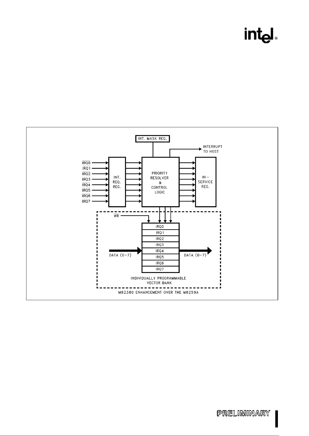
M82380
4.1.2 INTERRUPT CONTROLLER BANKS
All three banks are identical, with the exception of
the IRQ1.5 on Bank A. Therefore, only one bank will
be discussed. In the M82380 PIC, all external requests can be cascaded into and each interrupt controller bank behaves like a master. As compared to
the M8259A, the enhancements in the banks are:
Ð All interrupt vectors are individually programma-
ble. (In the M8259A, the vectors must be programmed in eight consecutive interrupt vector locations.)
Ð The cascade address is provided on the Data
Bus (D0–D7). (In the M8259A, three dedicated
control signals (CAS0, CAS1, CAS2) are used for
master/slave cascading.)
The block diagram of a bank is shown in Figure 38.
As can be seen from this figure, the bank consists of
six major blocks: the Interrupt Request Register
(IRR), the In-Service Register (ISR), the Interrupt
Mask Register (IMR), the Priority Resolver (PR), the
Vector Register (VR), and the Control Logic. The
functional description of each block follows.
271070–49
Figure 38. Interrupt Bank Block Diagram
54
Page 55

M82380
INTERRUPT REQUEST (IRR) AND IN-SERVICE
REGISTER (ISR)
The interrupts at the Interrupt Request (IRQ) input
lines are handled by two registers in cascade, the
Interrupt Request Register (IRR) and the In-Service
Register (ISR). The IRR is used to store all interrupt
levels which are requesting service; and the ISR is
used to store all interrupt levels which are being
serviced.
PRIORITY RESOLVER (PR)
This logic block determines the priorities of the bits
set in the IRR. The highest priority is selected and
strobed into the corresponding bit of the ISR during
an Interrupt Acknowledge cycle.
INTERRUPT MASK REGISTER (IMR)
The IMR stores the bits which mask the interrupt
lines to be masked (disabled). The IMR operates on
the IRR. Masking of a higher priority input will not
affect the interrupt request lines of lower priority.
VECTOR REGISTERS (VR)
This block contains a set of Vector Registers, one
for each interrupt request line, to store the pre-programmed interrupt vector number. The corresponding vector number will be driven onto the Data Bus
of the M82380 during the Interrupt Acknowledge cycle.
CONTROL LOGIC
The Control Logic coordinates the overall operations
of the other internal blocks within the same bank.
This logic will drive the Interrupt Output signal (INT)
HIGH when one or more unmasked interrupt inputs
are active (LOW). The INT output signal goes directly to the i386 processor (in Bank A) or to another
bank to which this bank is cascaded (see Figure 37).
Also, this logic will recognize an Interrupt Acknowledge cycle (via M/IO
, D/C and W/R signals). During
this bus cycle, the Control Logic will enable the corresponding Vector Register to drive the interrupt
vector onto the Data Bus.
In Bank A, the Control Logic is also responsible for
handling the special ICW2 interrupt request input
(IRQ1.5
).
4.2 Interface Signals
4.2.1 INTERRUPT INPUTS
There are 15 external Interrupt Request inputs and 5
internal Interrupt Requests. The external request inputs are: IRQ3
, IRQ9, IRQ11 to IRQ23. They are
shown in bold arrows in Figure 37. All IRQ inputs are
active LOW and they can be programmed (via a control bit in the Initialization Command Word 1 (ICW1))
to be either edge-triggered or level-triggered. In order to be recognized as a valid interrupt request, the
interrupt input must be active (LOW) until the first
INTA
cycle (see Bus Functional Description). Note
that all 15 external Interrupt Request inputs have
weak internal pull-up resistors.
As mentioned earlier, an M8259A can be cascaded
to each external interrupt input to expand the interrupt capacity to a maximum of 120 levels. Also, two
of the interrupt inputs are dual functions: IRQ3
can
be used as Timer 2 output (TOUT2
) and IRQ9
can
be used as DREQ4 input. IRQ3
is a bidirectional dual
function pin. This interrupt request input is wired-OR
with the output of Timer 2 (TOUT2
). If only IRQ3
function is to be used, Timer 2 should be programmed so that OUT2 is LOW. Note that TOUT2
can also be used to generate an interrupt request to
IRQ3
input.
The five internal interrupt requests serve special
system functions. They are shown in Table 8. The
following paragraphs describe these interrupts.
Table 8. M82380 Internal Interrupt Requests
Interrupt Request Interrupt Source
IRQ0 Timer 3 Output (TOUT3)
IRQ8
Timer 0 Output (TOUT0)
IRQ1
DMA Chaining Request
IRQ4
DMA Terminal Count
IRQ1.5
ICW2 Written
TIMER 0 AND TIMER 3 INTERRUPT REQUESTS
IRQ8
and IRQ0 interrupt requests are initiated by the
output of Timers 0 and 3, respectively. Each of these
requests is generated by an edge-detector flip-flop.
The flip-flops are activated by the following conditions:
SetÐ Rising edge of timer output (TOUT);
ClearÐ Interrupt acknowledge for this request;
OR Request is masked (disabled); OR
Hardware Reset.
55
Page 56
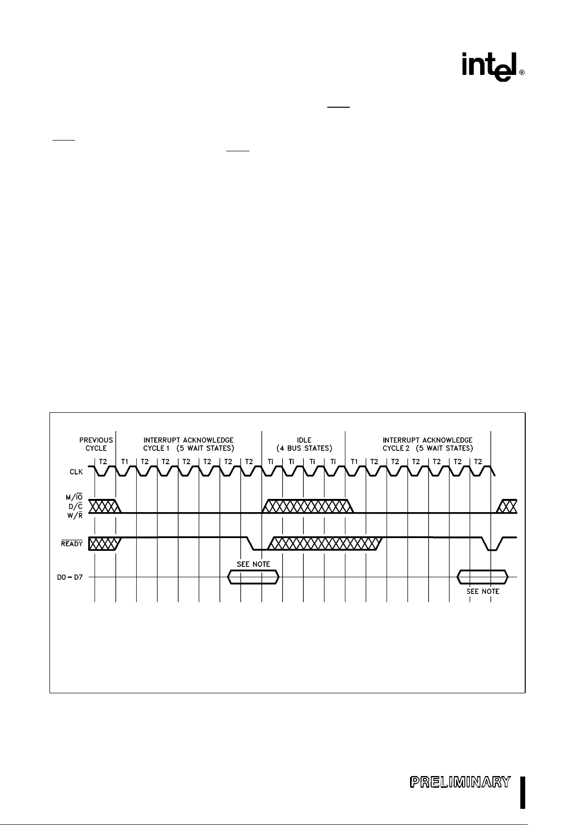
M82380
CHAINING AND TERMINAL COUNT INTERRUPTS
These interrupt requests are generated by the
M82380 DMA Controller. The chaining request
(IRQ1
) indicates that the DMA Base Register is not
loaded. The Terminal Count request (IRQ4
) indi-
cates that a software DMA request was cleared.
ICW2 INTERRUPT REQUEST
Whenever an Initialization Control Word 2 (ICW2) is
written to a Bank, a special ICW2 interrupt request is
generated. The interrupt will be cleared when the
newly programmed ICW2 Register is read. This interrupt request is in Bank A at level 1.5. This interrupt request is internally ORed with the Cascaded
Request from Bank B and is always assigned a higher priority than the Cascaded Request.
This special interrupt is provided to support compatibility with the original M8259A. A detailed description
of this interrupt is discussed in the Programming
section.
DEFAULT INTERRUPT
During an Interrupt Acknowledge cycle, if there is no
active pending request, the PIC will automatically
generate a default vector. This vector corresponds
to the IRQ7 vector in Bank A.
4.2.2 INTERRUPT OUTPUT (INT)
The INT output pin is taken directly from bank A.
This signal should be tied to the Maskable Interrupt
Request (INTR) of the i386 processor. When this
signal is active (HIGH), it indicates that one or more
internal/external interrupt requests are pending. The
i386 processor is expected to respond with an interrupt acknowledge cycle.
4.3 Bus Functional Description
The INT output of bank A will be activated as a result
of any unmasked interrupt request. This may be a
non-cascaded or cascaded request. After the PIC
has driven the INT signal HIGH, i386 processor will
respond by performing two interrupt acknowledge
cycles. The timing diagram in Figure 39 shows a typical interrupt acknowledge process between the
M82380 and the i386 CPU.
271070–50
NOTE:
What is actually driven on the Data Bus depends on if the current interrupt request is a Slave Request.
INTA Cycle 1 INTA Cycle 2
NON-SLAVE REQUEST 00H Vector
SLAVE REQUEST Slave Address High Impedance*
*Slave will place a vector at this time.
Figure 39. Interrupt Acknowledge Cycle
56
Page 57

M82380
After activating the INT signal, the M82380 monitors
the status lines (M/IO
, D/C, W/R) and waits for the
i386 processor to initiate the first interrupt acknowledge cycle. In the i386 processor environment, two
successive interrupt acknowledge cycles (INTA)
marked by M/IOeLOW, D/CeLOW, and W/R
e
LOW are performed. During the first INTA cycle, the
PIC will determine the highest priority request. Assuming this interrupt input has no external Slave
Controller cascaded to it, the M82380 will drive the
Data Bus with 00H in the first INTA cycle. During the
second INTA cycle, the M82380 PIC will drive the
Data Bus with the corresponding preprogrammed interrupt vector.
If the PIC determines (from the ICW3) that this interrupt input has an external Slave Controller cascaded
to it, it will drive the Data Bus with the specific Slave
Cascade Address (instead of 00H) during the first
INTA cycle. This Slave Cascade Address is the preprogrammed content in the corresponding Vector
Register. This means that no Slave Address should
be chosen to be 00H. Note that the Slave Address
and Interrupt Vector are different interpretations of
the same thing. They are both the contents of the
programmable Vector Register. During the second
INTA cycle, the Data Bus will be floated so that the
external Slave Controller can drive its interrupt vector on the bus. Since the Slave Interrupt Controller
resides on the system bus, bus transceiver enable
and direction control logic must take this into consideration.
In order to have a successful interrupt service, the
interrupt request input must be held active (LOW)
until the beginning of the first interrupt acknowledge
cycle. If there is no pending interrupt request when
the first INTA cycle is generated, the PIC will generate a default vector, which is the IRQ7 vector (bank
A level 7).
According to the Bus Cycle definition of the i386
processor, there will be four Bus Idle States between the two interrupt acknowledge cycles. These
idle bus cycles will be initiated by the i386 processor.
Also, during each interrupt acknowledge cycle, the
internal Wait State Generator of the M82380 will automatically generate the required number of wait
states for internal delays.
4.4 Mode of Operation
A variety of modes and commands are available for
controlling the M82380 PIC. All of them are programmable; that is, they may be changed dynamically under software control. In fact, each bank can be
programmed individually to operate in different
modes. With these modes and commands, many
possible configurations are conceivable, giving the
user enough versatility for almost any interrupt controlled application.
This section is not intended to show how the
M82380 PIC can be programmed. Rather, it describes the operation in different modes.
4.4.1 END-OF-INTERRUPT
Upon completion of an interrupt service routine, the
interrupted bank needs to be notified so its ISR can
be updated. This allows the PIC to keep track of
which interrupt levels are in the process of being
serviced and their relative priorities. Three different
End-Of-Interrupt (EOI) formats are available. They
are: Non-Specific EOI Command, Specific EOI Command, and Automatic EOI Mode. Selection of which
EOI to use is dependent upon the interrupt operations the user wishes to perform.
If the M82380 is NOT programmed in the Automatic
EOI Mode, an EOI command must be issued by the
i386 processor to the specific M82380 PIC Controller Bank. Also, if this controller bank is cascaded to
another internal bank, an EOI command must also
be sent to the bank to which this bank is cascaded.
For example, if an interrupt request of Bank C in the
M82380 PIC is serviced, an EOI should be written
into Bank C, Bank B and Bank A. If the request
comes from an external interrupt controller cascaded to Bank C, then an EOI should be written into the
external controller as well.
NON-SPECIFIC EOI COMMAND
A Non-Specific EOI command sent from the i386
processor lets the M82380 PIC bank know when a
service routine has been completed, without specification of its exact interrupt level. The respective interrupt bank automatically determines the interrupt
level and resets the correct bit in the ISR.
To take advantage of the Non-Specific EOI, the interrupt bank must be in a mode of operation in which
it can predetermine its in-service routine levels. For
this reason, the Non-Specific EOI command should
only be used when the most recent level acknowledged and serviced is always the highest priority level (i.e., in the Fully Nested Mode structure to be described below). When the interrupt bank receives a
Non-Specific EOI command, it simply resets the
highest priority ISR bit to indicate that the highest
priority routine in service is finished.
Special consideration should be taken when deciding to use the Non-Specific EOI command. Here are
two operating conditions in which it is best NOT
57
Page 58

M82380
used since the Fully Nested Mode structure will be
destroyed:
Ð Using the Set Priority command within an inter-
rupt service routine.
Ð Using a Special Mask Mode.
These conditions are covered in more detail in their
own sections, but are listed here for reference.
SPECIFIC EOI COMMAND
Unlike a Non-Specific EOI command which automatically resets the highest priority ISR bit, a Specific
EOI command specifies an exact ISR bit to be reset.
Any one of the IRQ levels of an interrupt bank can
be specified in the command.
The Specific EOI command is needed to reset the
ISR bit of a completed service routine whenever the
interrupt bank is not able to automatically determine
it. The Specific EOI command can be used in all
conditions of operation, including those that prohibit
Non-Specific EOI command usage mentioned
above.
AUTOMATIC EOI MODE
When programmed in the Automatic EOI Mode, the
M80386 no longer needs to issue a command to
notify the interrupt bank it has completed an interrupt routine. The interrupt bank accomplishes this by
performing a Non-Specific EOI automatically at the
end of the second INTA cycle.
Special consideration should be taken when deciding to use the Automatic EOI Mode because it may
disturb the Fully Nested Mode structure. In the Automatic EOI Mode, the ISR bit of a routine in service is
reset right after it is acknowledged, thus leaving no
designation in the ISR that a service routine is being
executed. If any interrupt request within the same
bank occurs during this time and interrupts are enabled, it will get serviced regardless of its priority.
Therefore, when using this mode, the M80386
should keep its interrupt request input disabled during execution of a service routine. By doing this,
higher priority interrupt levels will be serviced only
after the completion of a routine in service. This
guideline restores the Fully Nested Mode structure.
However, in this scheme, a routine in service cannot
be interrupted since the host’s interrupt request input is disabled.
4.4.2 INTERRUPT PRIORITIES
The M82380 PIC provides various methods for arranging the interrupt priorities of the interrupt request inputs to suit different applications. The following sub-sections explain these methods in detail.
FULLY NESTED MODE
The Fully Nested Mode of operation is a general purpose priority mode. This mode supports a multi-level
interrupt structure in which all of the Interrupt Request (IRQ) inputs within one bank are arranged
from highest to lowest.
Unless otherwise programmed, the Fully Nested
Mode is entered by default upon initialization. At this
time, IRQ0
is assigned the highest priority (priority
e
0) and IRQ7 the lowest (prioritye7). This default
priority can be changed, as will be explained later in
the Rotating Priority Mode.
When an interrupt is acknowledged, the highest priority request is determined from the Interrupt Request Register (IRR) and its vector is placed on the
bus. In addition, the corresponding bit in the In-Service Register (ISR) is set to designate the routine in
service. This ISR bit will remain set until the M80386
issues an End Of Interrupt (EOI) command immediately before returning from the service routine; or
alternately, if the Automatic End Of Interrupt (AEOI)
bit is set, the ISR bit will be reset at the end of the
second INTA cycle.
58
Page 59
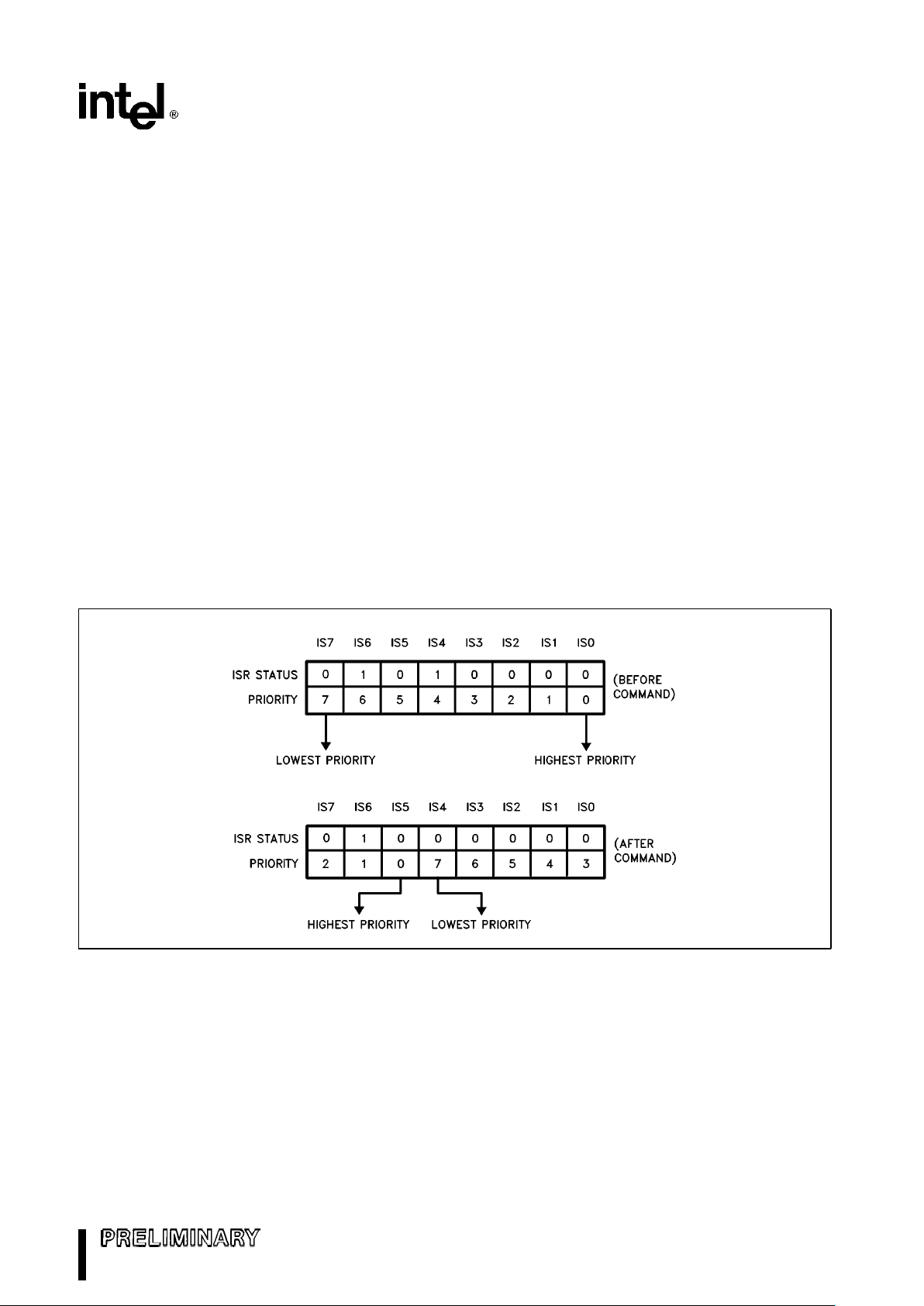
M82380
While the ISR bit is set, all further interrupts of the
same or lower priority are inhibited. Higher level interrupts can still generate an interrupt, which will be
acknowledged only if the i386 processor internal interrupt enable flip-flop has been re-enabled (through
software inside the current service routine).
AUTOMATIC ROTATIONÐEQUAL PRIORITY
DEVICES
Automatic rotation of priorities serves in applications
where the interrupting devices are of equal priority
within an interrupt bank. In this kind of environment,
once a device is serviced, all other equal priority peripherals should be given a chance to be serviced
before the original device is serviced again. This is
accomplished by automatically assigning a device
the lowest priority after being serviced. Thus, in the
worst case, the device would have to wait until all
other peripherals connected to the same bank are
serviced before it is serviced again.
There are two methods of accomplishing automatic
rotation. One is used in conjunction with the NonSpecific EOI command and the other is used with
the Automatic EOI mode. These two methods are
discussed below.
ROTATE ON NON-SPECIFIC EOI COMMAND
When the Rotate On Non-Specific EOI command is
issued, the highest ISR bit is reset as in a normal
Non-Specific EOI command. However, after it is reset, the corresponding Interrupt Request (IRQ) level
is assigned the lowest priority. Other IRQ priorities
rotate to conform to the Fully Nested Mode based
on the newly assigned low priority.
Figure 40 shows how the Rotate On Non-Specific
EOI command affects the interrupt priorities. Assume the IRQ priorities were assigned with IRQ0 the
highest and IRQ7 the lowest. IRQ6 and IRQ4 are
already in service but neither is completed. Being
the higher priority routine, IRQ4 is necessarily the
routine being executed. During the IRQ4 routine, a
rotate on Non-Specific EOI command is executed.
When this happens, Bit 4 in the ISR is reset. IRQ4
then becomes the lowest priority and IRQ5 becomes
the highest.
271070–51
271070–52
Figure 40. Rotate On Non-Specific EOI Command
59
Page 60

M82380
ROTATE ON AUTOMATIC EOI MODE
The Rotate On Automatic EOI Mode works much
like the Rotate On Non-Specific EOI Command. The
main difference is that priority rotation is done automatically after the second INTA cycle of an interrupt
request. To enter or exit this mode, a Rotate-On-Automatic-EOI Set Command and Rotate-On-Automatic-EOI Clear Command is provided. After this mode
is entered, no other commands are needed as in the
normal Automatic EOI Mode. However, it must be
noted again that when using any form of the Automatic EOI Mode, special consideration should be
taken. The guideline presented in the Automatic EOI
Mode also applies here.
SPECIFIC ROTATIONÐSPECIFIC PRIORITY
Specific rotation gives the user versatile capabilities
in interrupt controlled operations. It serves in those
applications in which a specific device’s interrupt priority must be altered. As opposed to Automatic Rotation which will automatically set priorities after
each interrupt request is serviced, specific rotation is
completely user controlled. That is, the user selects
which interrupt level is to receive the lowest or the
highest priority. This can be done during the main
program or within interrupt routines. Two specific rotation commands are available to the user: Set Priority Command and Rotate On Specific EOI Command.
SET PRIORITY COMMAND
The Set Priority Command allows the programmer to
assign an IRQ level the lowest priority. All other interrupt levels will conform to the Fully Nested Mode
based on the newly assigned low priority.
ROTATE ON SPECIFIC EOI COMMAND
The Rotate On Specific EOI Command is literally a
combination of the Set Priority Command and the
Specific EOI Command. Like the Set Priority Command, a specified IRQ level is assigned lowest priority. Like the Specific EOI Command, a specified level
will be reset in the ISR. Thus, this command accomplishes both tasks in one single command.
INTERRUPT PRIORITY MODE SUMMARY
In order to simplify understanding the many modes
of interrupt priority, Table 9 is provided to bring out
their summary of operations.
Table 9. Interrupt Priority Mode Summary
Interrupt Operation Effect On Priority After EOI
Priority Mode Summary
Non-Specific/Automatic Specific
Fully-Nested Mode IRQ0-Highest Priority No change in priority. Not Applicable.
IRQ7
-Lowest Priority Highest ISR bit is reset.
Automatic Rotation Interrupt level just serviced Highest ISR bit is reset and the Not Applicable.
is the lowest priority. Other
(Equal Priority Devices) corresponding level becomes the
priorities rotate to conform
lowest priority.
to Fully-Nested Mode.
Specific Rotation User specifies the lowest Not Applicable. As described under
priority level. Other priorities
(Specific Priority ‘Operation Summary’.
rotate to conform to Fully-
Devices)
Nested Mode.
60
Page 61
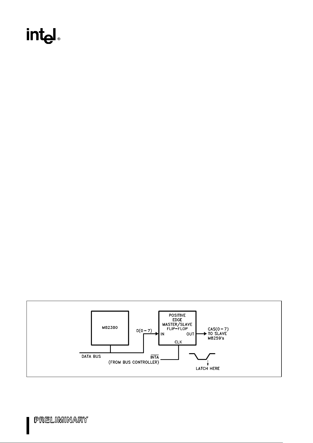
M82380
4.4.3 INTERRUPT MASKING
VIA INTERRUPT MASK REGISTER
Each bank in the M82380 PIC has an Interrupt Mask
Register (IMR) which enhances interrupt control capabilities. This IMR allows individual IRQ masking.
When an IRQ is masked, its interrupt request is disabled until it is unmasked. Each bit in the 8-bit IMR
disables one interrupt channel if it is set (HIGH). Bit
0 masks IRQ0, Bit 1 masks IRQ1 and so forth.
Masking an IRQ channel will only disable the corresponding channel and does not affect the others operations.
The IMR acts only on the output of the IRR. That is,
if an interrupt occurs while its IMR bit is set, this
request is not ‘forgotten’. Even with an IRQ input
masked, it is still possible to set the IRR. Therefore,
when the IMR bit is reset, an interrupt request to the
i386 processor will then be generated, providing that
the IRQ request remains active. If the IRQ request is
removed before the IMR is reset, the Default Interrupt Vector (Bank A, level 7) will be generated during
the interrupt acknowledge cycle.
SPECIAL MASK MODE
In the Fully Nested Mode, all IRQ levels of lower
priority than the routine in service are inhibited. However, in some applications, it may be desirable to let
a lower priority interrupt request to interrupt the routine in service. One method to achieve this is by
using the Special Mask Mode. Working in conjunction with the IMR, the Special Mask Mode enables
interrupts from all levels except the level in service.
This is usually done inside an interrupt service routine by masking the level that is in service and then
issuing the Special Mask Mode Command. Once the
Special Mask Mode is enabled, it remains in effect
until it is disabled.
4.4.4 EDGE OR LEVEL INTERRUPT
TRIGGERING
Each bank in the M82380 PIC can be programmed
independently for either edge or level sensing for the
interrupt request signals. Recall that all IRQ inputs
are active LOW. Therefore, in the edge triggered
mode, an active edge is defined as an input transition from an inactive (HIGH) to active (LOW) state.
The interrupt input may remain active without generating another interrupt. During level triggered mode,
an interrupt request will be recognized by an active
(LOW) input, and there is no need for edge detection. However, the interrupt request must be removed before the EOI Command is issued, or the
i386 processor must be disabled to prevent a second false interrupt from occurring.
In either modes, the interrupt request input must be
active (LOW) during the first INTA cycle in order to
be recognized. Otherwise, the Default Interrupt Vector will be generated at level 7 of Bank A.
4.4.5 INTERRUPT CASCADING
As mentioned previously, the M82380 allows for external Slave interrupt controllers to be cascaded to
any of its external interrupt request pins. The
M82380 PIC indicates that a external Slave Controller is to be serviced by putting the contents of the
Vector Register associated with the particular request on the i386 Data Bus during the first INTA
cycle (instead of 00H during a non-slave service).
The external logic should latch the vector on the
Data Bus using the INTA status signals and use it to
select the external Slave Controller to be serviced
(see Figure 41). The selected Slave will then respond to the second INTA cycle and place its vector
on the Data Bus. This method requires that if external Slave Controllers are used in the system, no vector should be programmed to 00H.
271070–53
Figure 41. Slave Cascade Address Capturing
61
Page 62

M82380
Since the external Slave Cascade Address is provided on the Data Bus during INTA cycle 1, an external
latch is required to capture this address for the Slave
Controller. A simple scheme is depicted in Figure 41.
SPECIAL FULLY NESTED MODE
This mode will be used where cascading is employed and the priority is to be conserved within
each Slave Controller. The Special Fully Nested
Mode is similar to the ‘regular’ Fully Nested Mode
with the following exceptions:
Ð When an interrupt request from a Slave Control-
ler is in service, this Slave Controller is not
locked out from the Master’s priority logic. Further interrupt requests from the higher priority
logic within the Slave Controller will be recognized by the M82380 PIC and will initiate interrupts to the i386 processor. In comparing to the
‘regular’ Fully Nested Mode, the Slave Controller
is masked out when its request is in service and
no higher requests from the same Slave Controller can be serviced.
Ð Before exiting the interrupt service routine, the
software has to check whether the interrupt serviced was the only request from the Slave Controller. This is done by sending a Non-Specific
EOI Command to the Slave Controller and then
reading its In Service Register. If there are no
requests in the Slave Controller, a Non-Specific
EOI can be sent to the corresponding M82380
PIC bank also. Otherwise, no EOI should be
sent.
4.4.6 READING INTERRUPT STATUS
The M82380 PIC provides several ways to read different status of each interrupt bank for more flexible
interrupt control operations. These include polling
the highest priority pending interrupt request and
reading the contents of different interrupt status registers.
POLL COMMAND
The M82380 PIC supports status polling operations
with the Poll Command. In a Poll Command, the
pending interrupt request with the highest priority
can be determined. To use this command, the INT
output is not used, or the i386 processor interrupt is
disabled. Service to devices is achieved by software
using the Poll Command.
This mode is useful if there is a routine command
common to several levels so that the INTA sequence is not needed. Another application is to use
the Poll Command to expand the number of priority
levels.
Notice that the ICW2 mechanism is not supported
for the Poll Command. However, if the Poll Command is used, the programmable Vector Registers
are of no concern since no INTA cycle will be generated.
READING INTERRUPT REGISTERS
The contents of each interrupt register (IRR, ISR,
and IMR) can be read to update the user’s program
on the present status of the M82380 PIC. This can
be a versatile tool in the decision making process of
a service routine, giving the user more control over
interrupt operations.
The reading of the IRR and ISR contents can be
performed via the Operation Control Word 3 by using a Read Status Register Command and the content of IMR can be read via a simple read operation
of the register itself.
4.5 Register Set Overview
Each bank of the M82380 PIC consists of a set of
8-bit registers to control its operations. The address
map of all the registers is shown in Table 10. Since
all three register sets are identical in functions, only
one set will be described.
Functionally, each register set can be divided into
five groups. They are: the four Initialization Command Words (ICW’s), the three Operation Control
Words (OCW’s), the Poll/Interrupt Request/In-Service Register, the Interrupt Mask Register, and the
Vector Registers. A description of each group follows.
62
Page 63

M82380
Table 10. Interrupt Controller Register Address Map
Port
Access Register Description
Address
20H Write Bank B ICW1, OCW2, or OCW3
Read Bank B Poll, Request or In-Service
Status Register
21H Write Bank B ICW2, ICW3, ICW4, OCW1
Read Bank B Mask Register
22H Read Bank B ICW2
28H Read/Write IRQ8 Vector Register
29H Read/Write IRQ9 Vector Register
2AH Read/Write Reserved
2BH Read/Write IRQ11 Vector Register
2CH Read/Write IRQ12 Vector Register
2DH Read/Write IRQ13 Vector Register
2EH Read/Write IRQ14 Vector Register
2FH Read/Write IRQ15 Vector Register
A0H Write Bank C ICW1, OCW2, or OCW3
Read Bank C Poll, Request or In-Service
Status Register
A1H Write Bank C ICW2, ICW3, ICW4, OCW1
Read Bank C Mask Register
A2H Read Bank C ICW2
A8H Read/Write IRQ16 Vector Register
A9H Read/Write IRQ17 Vector Register
AAH Read/Write IRQ18 Vector Register
ABH Read/Write IRQ19 Vector Register
ACH Read/Write IRQ20 Vector Register
ADH Read/Write IRQ21 Vector Register
AEH Read/Write IRQ22 Vector Register
AFH Read/Write IRQ23 Vector Register
30H Write Bank A ICW1, OCW2, or OCW3
Read Bank A Poll, Request or In-Service
Status Register
31H Write Bank A ICW2, ICW3, ICW4, OCW1
Read Bank A Mask Register
32H Read Bank ICW2
38H Read/Write IRQ0 Vector Register
39H Read/Write IRQ1 Vector Register
3AH Read/Write IRQ1.5 Vector Register
3BH Read/Write IRQ3 Vector Register
3CH Read/Write IRQ4 Vector Register
3DH Read/Write Reserved
3EH Read/Write Reserved
3FH Read/Write IRQ7 Vector Register
63
Page 64

M82380
4.5.1 INITIALIZATION COMMAND WORDS (ICW)
Before normal operation can begin, the M82380 PIC
must be brought to a known state. There are four
8-bit Initialization Command Words in each interrupt
bank to setup the necessary conditions and modes
for proper operation. Except for the second common
word (ICW2) which is a read/write register, the other
three are write-only registers. Without going into detail of the bit definitions of the command words, the
following subsections give a brief description of what
functions each command word controls.
ICW1
The ICW1 has three major functions. They are:
Ð To select between the two IRQ input triggering
modes (edge-or level-triggered);
Ð To designate whether or not the interrupt bank is
to be used alone or in the cascade mode. If the
cascade mode is desired, the interrupt bank will
accept ICW3 for further cascade mode programming. Otherwise, no ICW3 will be accepted;
Ð To determine whether or not ICW4 will be issued;
that is, if any of the ICW4 operations are to be
used.
ICW2
ICW2 is provided for compatibility with the M8259A
only. Its contents do not affect the operation of the
interrupt bank in any way. Whenever the ICW2 of
any of the three banks is written into, an interrupt is
generated from Bank A at level 1.5. The interrupt
request will be cleared after the ICW2 register has
been read by the M80386. The user is expected to
program the corresponding vector register or to use
it as an indicator that an attempt was made to alter
the contents. Note that each ICW2 register has different addresses for read and write operations.
ICW3
The interrupt bank will only accept an ICW3 if programmed in the external cascade mode (as indicated in ICW1). ICW3 is used for specific programming
within the cascade mode. The bits in ICW3 indicate
which interrupt request inputs have a Slave cascaded to them. This will subsequently affect the interrupt vector generation during the interrupt acknowledge cycles as described previously.
ICW4
The ICW4 is accepted only if it was selected in
ICW1. This command word register serves two functions:
Ð To select either the Automatic EOI mode or soft-
ware EOI mode;
Ð To select if the Special Nested mode is to be
used in conjunction with the cascade mode.
4.5.2 OPERATION CONTROL WORDS (OCW)
Once initialized by the ICW’s, the interrupt banks will
be operating in the Fully Nested Mode by default
and they are ready to accept interrupt requests.
However, the operations of each interrupt bank can
be further controlled or modified by the use of
OCW’s. Three OCW’s are available for programming
various modes and commands. Note that all OCW’s
are 8-bit write-only registers.
The modes and operations controlled by the OCW’s
are:
Ð Fully Nested Mode;
Ð Rotating Priority Mode;
Ð Special Mask Mode;
Ð Poll Mode;
Ð EOI Commands;
Ð Read Status Commands.
OCW1
OCW1 is used solely for masking operations. It provides a direct link to the Interrupt Mask Register
(IMR). The M80386 can write to this OCW register to
enable or disable the interrupt inputs. Reading the
pre-programmed mask can be done via the Interrupt
Mask Register which will be discussed shortly.
OCW2
OCW2 is used to select End-Of-Interrupt, Automatic
Priority Rotation, and Specific Priority Rotation operations. Associated commands and modes of these
operations are selected using the different combinations of bits in OCW2.
Specifically, the OCW2 is used to:
Ð Designate an interrupt level (0–7) to be used to
reset a specific ISR bit or to set a specific priority. This function can be enabled or disabled;
Ð Select which software EOI command (if any) is to
be executed (i.e., Non-Specific or Specific EOI);
Ð Enable one of the priority rotation operations
(i.e., Rotate On Non-Specific EOI, Rotate On Automatic EOI, or Rotate on Specific EOI).
OCW3
There are three main categories of operation that
OCW3 controls. That are summarized as follows:
64
Page 65

M82380
Ð To select and execute the Read Status Register
Commands, either reading the Interrupt Request
Register (IRR) or the In-Service Register (ISR);
Ð To issue the Poll Command. The Poll Command
will override a Read Register Command if both
functions are enabled simultaneously;
Ð To set or reset the Special Mask Mode.
4.5.3 POLL/INTERRUPT REQUEST/IN-SERVICE
STATUS REGISTER
As the name implies, this 8-bit read-only register has
multiple functions. Depending on the command issued in the OCW3, the content of this register reflects the result of the command executed. For a
Poll Command, the register read contains the binary
code of the highest priority level requesting service
(if any). For a Read IRR Command, the register content will show the current pending interrupt request(s). Finally, for a Read ISR Command, this register will specify all interrupt levels which are being
serviced.
4.5.4 INTERRUPT MASK REGISTER (IMR)
This is a read-only 8-bit register which, when read,
will specify all interrupt levels within the same bank
that are masked.
4.5.5 VECTOR REGISTER (VR)
Each interrupt request input has an 8-bit read/write
programmable vector register associated with it. The
registers should be programmed to contain the interrupt vector for the corresponding request. The contents of the Vector Register will be placed on the
Data Bus during the INTA cycles as described previously.
4.6 Programming
Programming the M82380 PIC is accomplished by
using two types of command words: ICW’s and
OCW’s. All modes and commands explained in the
previous sections are programmable using the
ICW’s and OCW’s. The ICW’s are issued from the
M80386 in a sequential format and are used to setup the banks in the M82380 PIC in an initial state of
operation. The OCW’s are issued as needed to vary
and control the M82380 PIC’s operations.
Both ICW’s and OCW’s are sent by the i386 processor to the interrupt banks via the Data Bus. Each
bank distinguishes between the different ICW’s and
OCW’s by the I/O address map, the sequence they
are issued (ICW’s only), and by some dedicated bits
among the ICW’s and OCW’s.
All three interrupt banks are programmed in a similar
way. Therefore, only a single bank will be described.
4.6.1 INITIALIZATION (ICW)
Before normal operation can begin, each bank must
be initialized by programming a sequence of two to
four bytes written into the ICW’s.
Figure 42 shows the initialization flow for an interrupt
bank. Both ICW1 and ICW2 must be issued for any
form of operation. However, ICW3 and ICW4 are
used only if designated in ICW1. Once initialized, if
any programming changes within the ICW’s are to
be made, the entire ICW sequence must be reprogrammed, not just an individual ICW.
Note that although the ICW2’s in the M82380 PIC do
not affect the Bank’s operation, they still must be
programmed in order to preserve the compatibility
with the M8259A. The contents programmed are not
relevant to the overall operations of the interrupt
banks. Also, whenever one of the three ICW2’s is
programmed, an interrupt level 1.5 in Bank A will be
generated. This interrupt request will be cleared
upon reading of the ICW2 registers. Since the three
ICW2’s share the same interrupt level and the system may not know the origin of the interrupt, all three
ICW2’s must be read.
However, it is not necessary to provide an interrupt
service routine for the ICW2 interrupt. One way to
avoid this is as follows. At the beginning of the initialization of the interrupt banks, the i386 processor interrupt should be disabled. After each ICW2 register
write operation is performed during the initialization,
the corresponding ICW2 register is read. This read
operation will clear the interrupt request of the
M82380. At the end of the initialization, the i386
processor interrupt is re-enabled. With this method,
the i386 processor will not detect the ICW2 interrupt
request, thus eliminating the need of an interrupt
service routine.
Certain internal setup conditions occur automatically
within the interrupt bank after the first ICW (ICW1)
has been issued. They are:
Ð The edge sensitive circuit is reset, which means
that following initialization, an interrupt request
input must make a HIGH-to-LOW transition to
generate an interrupt;
Ð The Interrupt Mask Register (IMR) is cleared;
that is, all interrupt inputs are enabled;
Ð IRQ7 input of each bank is assigned priority 7
(lowest);
Ð Special Mask Mode is cleared and Status Read
is set to IRR;
Ð If no ICW4 is needed, then no Automatic-EOI is
selected.
65
Page 66
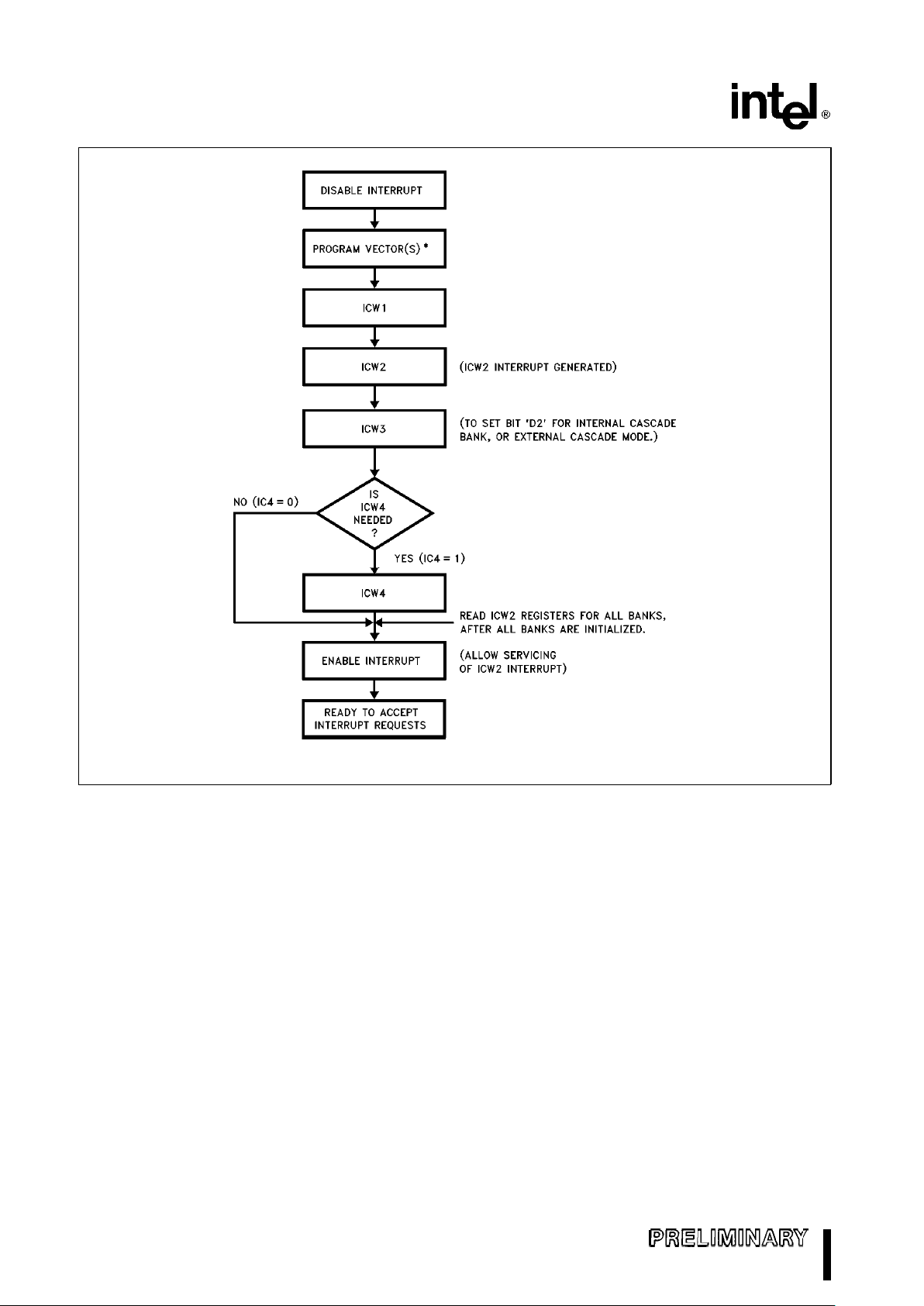
M82380
271070–54
*ICW2 vector address must be programmed now.
Other vector addresses may be programmed via ICW2 interrupt service routine.
Figure 42. Initialization Sequence
4.6.2 VECTOR REGISTERS (VR)
Each interrupt request input has a separate Vector
Register. These Vector Registers are used to store
the pre-programmed vector number corresponding
to their interrupt sources. In order to guarantee proper interrupt handling, all Vector Registers must be
programmed with the predefined vector numbers.
Since an interrupt request will be generated whenever an ICW2 is written during the initialization sequence, it is important that the Vector Register of
IRQ1.5 in Bank A should be initialized and the interrupt service routine of this vector is set up before the
ICW’s are written.
4.6.3 OPERATION CONTROL WORDS (OCW)
After the ICW’s are programmed, the operations of
each interrupt controller bank can be changed by
writing into the OCW’s as explained before. There is
no special programming sequence required for the
OCW’s. Any OCW may be written at any time in order to change the mode of or to perform certain operations on the interrupt banks.
READ STATUS AND POLL COMMANDS (OCW3)
Since the reading of IRR and ISR status as well as
the result of a Poll Command are available on the
66
Page 67

M82380
same read-only Status Register, a special Read
Status/Poll Command must be issued before the
Poll/Interrupt Request/In-Service Status Register is
read. This command can be specified by writing the
required control word into OCW3. As mentioned earlier, if both the Poll Command and the Status Read
Command are enabled simultaneously, the Poll
Command will override the Status Read. That is, after the command execution, the Status Register will
contain the result of the Poll Command.
Note that for reading IRR and ISR, there is no need
to issue a Read Status Command to the OCW3 every time the IRR or ISR is to be read. Once a Read
Status Command is received by the interrupt bank, it
‘remembers’ which register is selected. However,
this is not true when the Poll Command is used.
In the Poll Command, after the OCW3 is written, the
M82380 PIC treats the next read to the Status Register as an interrupt acknowledge. This will set the
appropriate IS bit if there is a request and read the
priority level. Interrupt Request input status remains
unchanged from the Poll Command to the Status
Read.
In addition to the above read commands, the Interrupt Mask Register (IMR) can also be read. When
read, this register reflects the contents of the preprogrammed OCW1 which contains information on
which interrupt request(s) is(are) currently disabled.
4.7 Register Bit Definition
INITIALIZATION COMMAND WORD 1 (ICW1)
271070–55
INITIALIZATION COMMAND WORD 2 (ICW2)
271070–56
67
Page 68
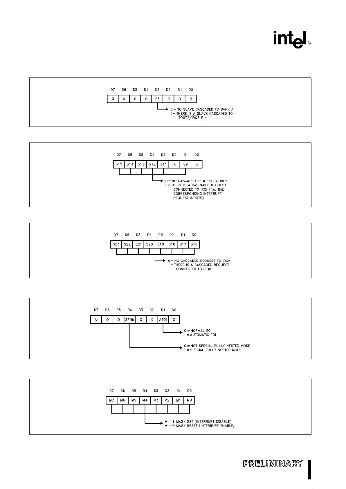
M82380
INITIALIZATION COMMAND WORD 3 (ICW3)
ICW3 for Bank A:
271070–57
ICW3 for Bank B:
271070–58
ICW3 for Bank C:
271070–59
INITIALIZATION COMMAND WORD 4 (ICW4)
271070–60
OPERATION CONTROL WORD 1 (OCW1)
271070–61
68
Page 69
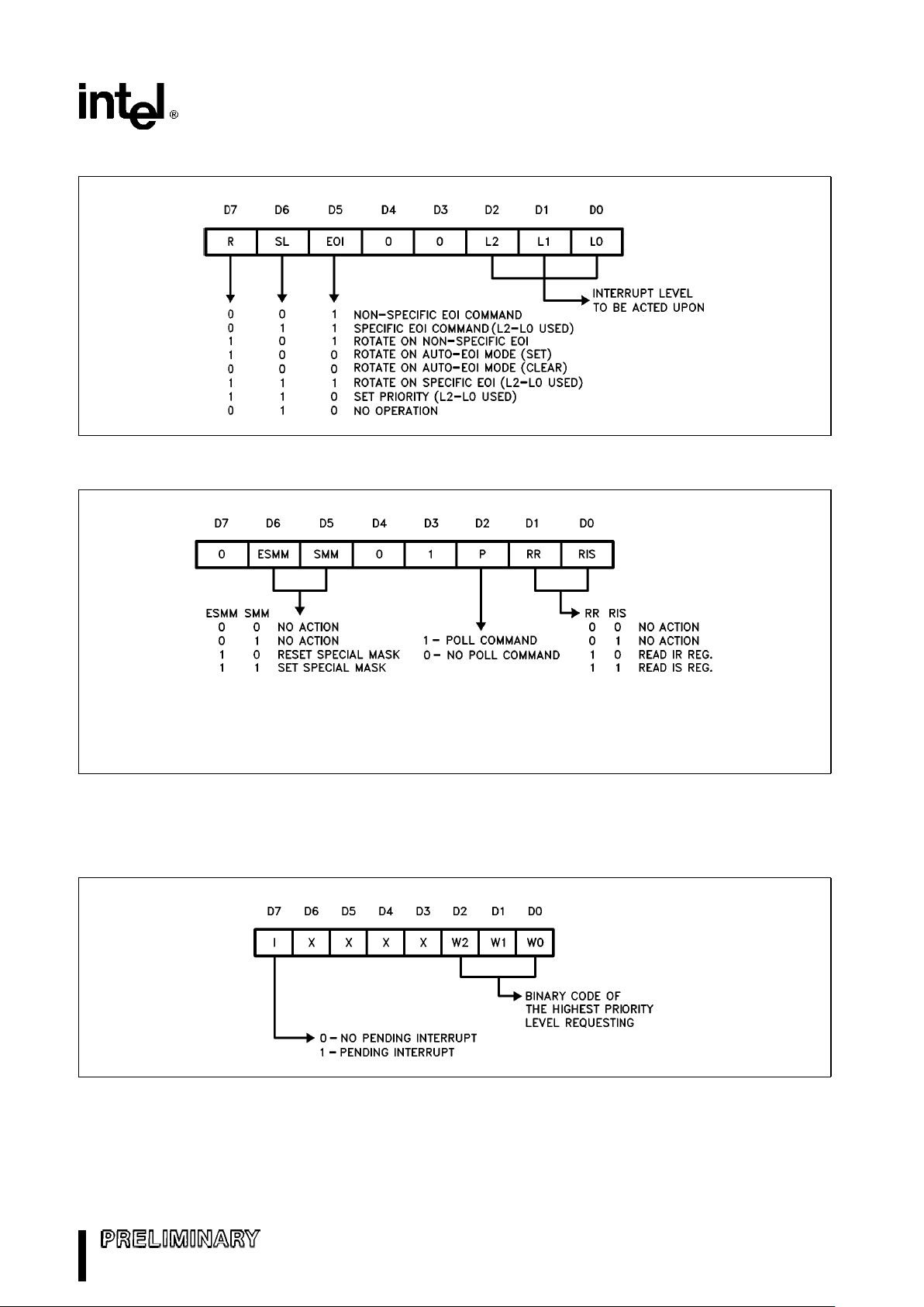
M82380
OPERATION CONTROL WORD 2 (OCW2)
271070–62
OPERATION CONTROL WORD 3 (OCW3)
271070–63
ESMMÐEnable Special Mask Mode. When this bit is set to 1, it enables the SMM bit to set or reset the Special Mask
Mode. When this bit is set to 0, SMM bit becomes don’t care.
SMMÐSpecial Mask Mode. If ESMM
e
1 and SMMe1, the interrupt controller bank will enter Special Mask Mode. If
ESMM
e
1 and SMMe0, the bank will revert to normal mask mode. When ESMMe0, SMM has no effect.
Poll/Interrupt Request/In-Service Status Register
POLL COMMAND STATUS
271070–64
69
Page 70

M82380
INTERRUPT REQUEST STATUS
271070–65
NOTE:
Although all Interrupt Request inputs are active LOW, the internal logical will invert the state of the pins so that when
there is a pending interrupt request at the input, the corresponding IRQ bit will be set to HIGH in the Interrupt Request
Status register.
IN-SERVICE STATUS
271070–66
VECTOR REGISTER (VR)
271070–67
4.8 Register Operational Summary
For ease of reference, Table 11 gives a summary of the different operating modes and commands with their
corresponding registers.
Table 11. Register Operational Summary
Operational Command
Bits
Description Words
Fully Nested Mode OCW-Default Ð
Non-specific EOI Command OCW2 EOI
Specific EOI Command OCW2 SL, EOI,
LO–L2
Automatic EOI Mode ICW1, ICW4 IC4, AEOI
Rotate On Non-Specific OCW2 EOI
EOI Command
Rotate On Automatic OCW2 R, SL, EOI
EOI Mode
Set Priority Command OCW2 L0– L2
Rotate On Specific OCW2 R, SL, EOI
EOI Command
Interrupt Mask Register OCW1 M0 –M7
Special Mask Mode OCW3 ESMM, SMM
Level Triggered Mode ICW1 LTIM
Edge Triggered Mode ICW1 LTIM
Read Register Command, IRR OCW3 RR, RIS
Read Register Command, ISR OCW3 RR, RIS
Red IMR IMR M0– M7
Poll Command OCW3 P
Special Fully Nested Mode ICW2, ICW4 IC4, SFNM
70
Page 71
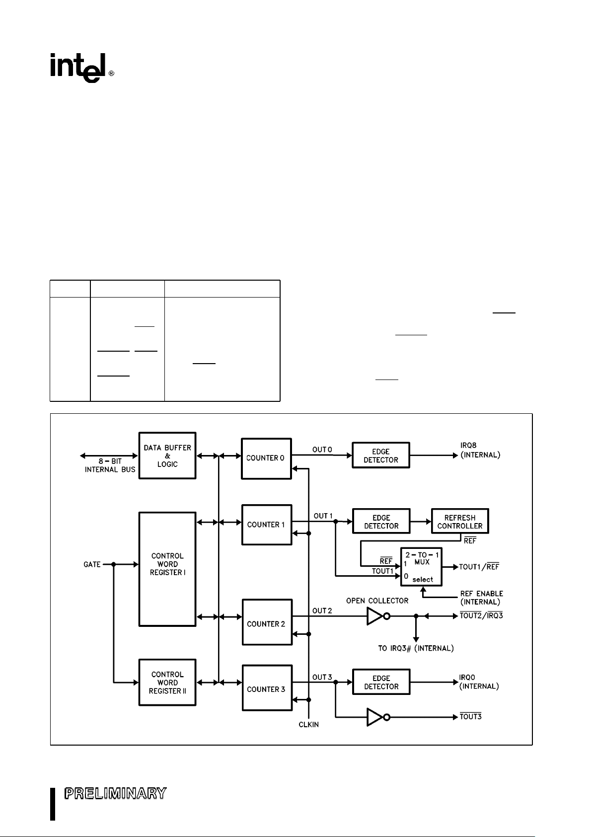
M82380
5.0 PROGRAMMABLE INTERVAL
TIMER
5.1 Functional Description
The M82380 contains four independently Programmable Interval Timers: Timer 0– 3. All four timers are
functionally compatible to the Intel M82C54. The
first three timers (Timer 0 –2) have specific functions. The fourth timer, Timer 3, is a general purpose
timer. Table 12 depicts the functions of each timer.
A brief description of each timer’s function follows.
Table 12. Programmable
Interval Timer Functions
Timer Output Function
0 IRQ8 Event Based
IRQ8 Generator
1 TOUT1/REF Gen. Purpose/DRAM
Refresh Req.
2 TOUT2/IRQ3 Gen. Purpose/Speaker
Out/IRQ3
3 TOUT3 Gen. Purpose/IRQ0
Generator
TIMER 0Ð Event Based IRQ8 Generator
Timer 0 is intended to be used as an Event Counter.
The output of this timer will generate an Interrupt
Request 8 (IRQ8) upon a rising edge of the timer
output (TOUT0). Typically, this timer is used to implement a time-of-day clock or system tick. The Timer 0 output is not available as an external signal.
TIMER 1Ð General Purpose/DRAM Refresh
Request
The output of Timer 1, TOUT1, can be used as a
general purpose timer or as a DRAM Refresh Request signal. The rising edge of this output creates a
DRAM refresh request to the M82380 DRAM Refresh Controller. Upon reset, the Refresh Request
function is disabled, and the output pin is the Timer 1
output.
TIMER 2ÐGeneral Purpose/Speaker Out/IRQ3
The Timer 2 output, TOUT2, could be used to support tone generation to an external speaker. This pin
is a bidirectional signal. When used as an input, a
logic LOW asserted at this pin will generate an Interrupt Register 3 (IRQ3) (see Programmable Interrupt
Controller).
271070–68
Figure 43. Block Diagram of Programmable Interval Timer
71
Page 72

M82380
TIMER 3ÐGeneral Purpose/Interrupt Request 0
Generator
The output of Timer 3 is fed to an edge detector and
generates an Interrupt Request 0 (IRQ0) in the
M82380. The inverted output of this timer (TOUT3
)
is also available as an external signal for general
purpose use.
5.1.1 INTERNAL ARCHITECTURE
The functional block diagram of the Programmable
Interval Timer section is shown in Figure 43. Following is a description of each block.
DATA BUFFER & READ/WRITE LOGIC
This part of the Programmable Interval Timer is used
to interface the four timers to the M82380 internal
bus. The Data Buffer is for transferring commands
and data between the 8-bit internal bus and the
timers.
The Read/Write Logic accepts inputs from the internal bus and generates signals to control other functional blocks within the timer section.
CONTROL WORD REGISTERS I & II
The Control Word Registers are write-only registers.
They are used to control the operating modes of the
timers. Control Word Register I controls Timers 0, 1
and 2, and Control Word Register II controls Timer
3. Detailed description of the Control Word Registers will be included in the Register Set Overview
section.
COUNTER 0, COUNTER 1,
COUNTER 2, COUNTER 3
Counters 0, 1, 2, and 3 are the major parts of Timers
0, 1, 2, and 3, respectively. These four functional
blocks are identical in operation, so only a single
counter will be described. The internal block diagram of one counter is shown in Figure 44.
The four counters share a common clock input
(CLKIN), but otherwise are fully independent. Each
counter is programmable to operate in a different
Mode.
Although the Control Word Register is shown in the
Figure 44, it is not part of the counter itself. Its programmed contents are used to control the operations of the counters.
271070–69
Figure 44. Internal Block Diagram of A Counter
72
Page 73

M82380
The Status Register, when latched, contains the current contents of the Control Word Register and
status of the output and Null Count Flag (see Read
Back Command).
The Counting Element (CE) is the actual counter. It
is a 16-bit presettable synchronous down counter.
The Output Latches (OL) contain two 8-bit latches
(OLM and OLL). Normally, these latches ‘follow’ the
content of the CE. OLM contains the most significant byte of the counter and OLL contains the least
significant byte. If the Counter Latch Command is
sent to the counter, OL will latch the present count
until read by the i386 processor and then return to
follow the CE. One latch at a time is enabled by the
timer’s Control Logic to drive the internal bus. This is
how the 16-bit Counter communicates over the 8-bit
internal bus. Note that CE cannot be read. Whenever the count is read, it is one of the OL’s that is being
read.
When a new count is written into the counter, the
value will be stored in the Count Registers (CR), and
transferred to CE. The transferring of the contents
from CR’s to CE is defined as ‘loading’ of the counter. The Count Register contains two 8-bit registers:
CRM (which contains the most significant byte) and
CRL (which contains the least significant byte). Similar to the OL’s, the Control Logic allows one register
at a time to be loaded from the 8-bit internal bus.
However, both bytes are transferred from the CR’s
to the CE simultaneously. Both CR’s are cleared
when the Counter is programmed. This way, if the
Counter has been programmed for one byte count
(either the most significant or the least significant
byte only), the other byte will be zero. Note that CE
cannot be written into directly. Whenever a count is
written, it is the CR that is being written.
As shown in the diagram, the Control Logic consists
of three signals: CLKIN, GATE, and OUT. CLKIN
and GATE will be discussed in detail in the section
that follows. OUT is the internal output of the counter. The external outputs of some timers (TOUT) are
the inverted version of OUT (see TOUT1, TOUT2
,
TOUT3
). The state of OUT depends on the mode of
operation of the timer.
5.2 Interface Signals
5.2.1 CLKIN
CLKIN is an input signal used by all four timers for
internal timing reference. This signal can be inde-
pendent of the M82380 system clock, CLK2. In the
following discussion, each ‘CLK Pulse’ is defined as
the time period between a rising edge and a falling
edge, in that order, of CLKIN.
During the rising edge of CLKIN, the state of GATE
is sampled. All new counts are loaded and counters
are decremented on the falling edge of CLKIN.
Please note that there are no restrictions on the
CLKIN signal during WRITE cycles to the M82380
timer unit. Refer to Appendix D for details on this
issue.
5.2.2 TOUT1, TOUT2
, TOUT3
TOUT1, TOUT2 and TOUT3 are the external output
signals of Timer 1, Timer 2 and Timer 3, respectively. TOUT2
and TOUT3 are the inverted signals of
their respective counter outputs, OUT. There is no
external output for Timer 0.
If Timer 2 is to be used as a tone generator of a
speaker, external buffering must be used to provide
sufficient drive capability.
The Outputs of Timer 2 and 3 are dual function pins.
The output pin of Timer 2 (TOUT2
/IRQ3), which is a
bidirectional open-collector signal, can also be used
as interrupt request input. When the interrupt function is enabled (through the Programmable Interrupt
Controller), a LOW on this input will generate an Interrupt Request 3 (IRQ3
) to the M82380 Programmable Interrupt Controller. This pin has a weak internal pull-up resistor. To use the IRQ3
function, Timer
2 should be programmed so that OUT2 is LOW. Additionally, OUT3 of Timer 3 is connected to an edge
detector which will generate an Interrupt Request 0
(IRQ0) to the M82380 after the rising edge of OUT3
(see Figure 43).
5.2.3 GATE
GATE is not an externally controllable signal. Rather, it can be software controlled with the Internal
Control Port. The state of GATE is always sampled
on the rising edge of CLKIN. Depending on the
mode of operation, GATE is used to enable/disable
counting or trigger the start of an operation.
For Timer 0 and 1, GATE is always enabled (HIGH).
For Timer 2 and 3, GATE is connected to Bit 0 and
6, respectively, of an Internal Control Port (at address 61H) of the M82380. After a hardware reset,
the state of GATE of Timer 2 and 3 is disabled
(LOW).
73
Page 74

M82380
5.3 Modes of Operation
Each timer can be independently programmed to
operate in one of six different modes. Timers are
programmed by writing a Control Word into the control Word Register followed by an Initial Count (see
Programming).
The following are defined for use in describing the
different modes of operation.
CLK PulseÐA rising edge, then a falling edge, in
that order of CLKIN.
TriggerÐA rising edge of a timer’s GATE input.
Timer/Counter LoadingÐThe transfer of a count
from Count Register (CR) to Count Element
(CE).
5.3.1 MODE 0ÐINTERRUPT ON TERMINAL
COUNT
Mode 0 is typically used for event counting. After the
Control Word is written, OUT is initially LOW, and will
remain LOW until the counter reaches zero. OUT
then goes HIGH and remains HIGH until a new
count or a new Mode 0 Control Word is written into
the counter.
In this mode, GATE
e
HIGH enables counting;
GATE
e
LOW disables counting. However, GATE
has no effect on OUT.
After the Control Word and initial count are written to
a timer, the initial count will be loaded on the next
CLK pulse. This CLK pulse does not decrement the
count, so for an initial count of N, OUT does not go
HIGH until N
a
1 CLK pulses after the initial count is
written.
If a new count is written to the timer, it will be loaded
on the next CLK pulse and counting will continue
from the new count. If a two-byte count is written,
the following happens:
1. Writing the first byte disables counting, OUT is set
LOW immediately (i.e., no CLK pulse required).
2. Writing the second byte allows the new count to
be loaded on the next CLK pulse.
This allows the counting sequence to be synchronized by software. Again, OUT does not go HIGH until
N
a
1 CLK pulses after the new count of N is writ-
ten.
If an initial count is written while GATE is LOW, the
counter will be loaded on the next CLK pulse. When
GATE goes HIGH, OUT will go HIGH N CLK pulses
later; no CLK pulse is needed to load the counter as
this has already been done.
5.3.2 MODE 1ÐGATE RETRIGGERABLE
ONE-SHOT
In this mode, OUT will be initially HIGH. OUT will go
LOW on the CLK pulse following a trigger to start the
one-shot operation. The OUT signal will then remain
LOW until the timer reaches zero. At this point, OUT
will stay HIGH until the next trigger comes in. Since
the state of GATE signals of Timer 0 and 1 are internally set to HIGH.
After writing the Control Word and initial count, the
timer is considered ‘armed’. A trigger results in loading the timer and setting OUT LOW on the next CLK
pulse. Therefore, an initial count of N will result in a
one-shot pulse width of N CLK cycles. Note that this
one-shot operation is retriggerable; i.e., OUT will remain LOW for N CLK pulses after every trigger. The
one-shot operation can be repeated without rewriting the same count into the timer.
If a new count is written to the timer during a oneshot operation, the current one-shot pulse width will
not be affected until the timer is retriggered. This is
because loading of the new count to CE will occur
only when the one-shot is triggered.
74
Page 75
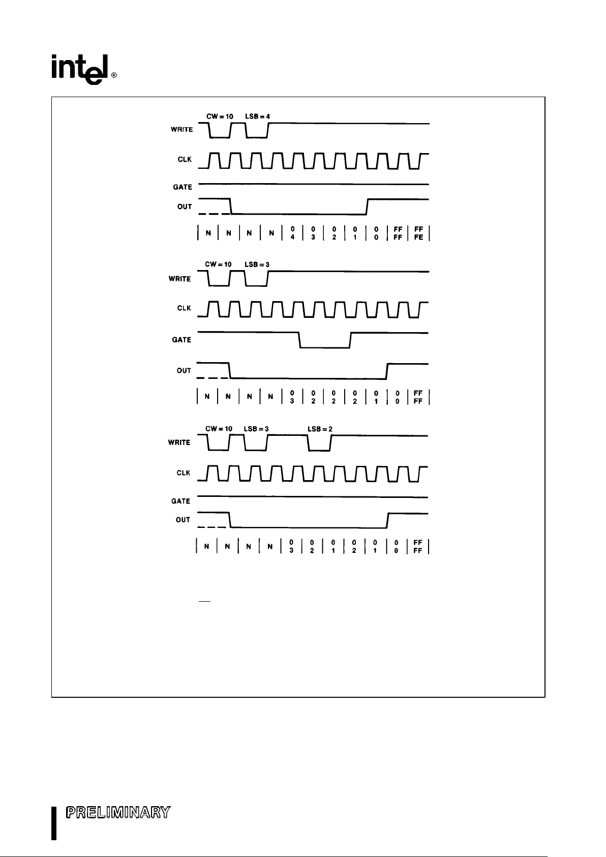
M82380
271070–70
NOTES:
The following conventions apply to all mode timing diagrams.
1. Counters are programmed for binary (not BCD) counting and for reading/writing least significant byte (LSB) only.
2. The counter is always selected (CS
always low).
3. CW stands for ‘‘Control Word’’; CW
e
10 means a control word of 10, Hex is written to the counter.
4. LSB stands for ‘‘least significant byte’’ of count.
5. Numbers below diagrams are count values.
The lower number is the least significant byte.
The upper number is the most significant byte. Since the counter is programmed to read/write LSB only, the
most significant byte cannot be read.
N stands for an undefined count.
Vertical lines show transitions between count values.
Figure 43. Mode 0
75
Page 76
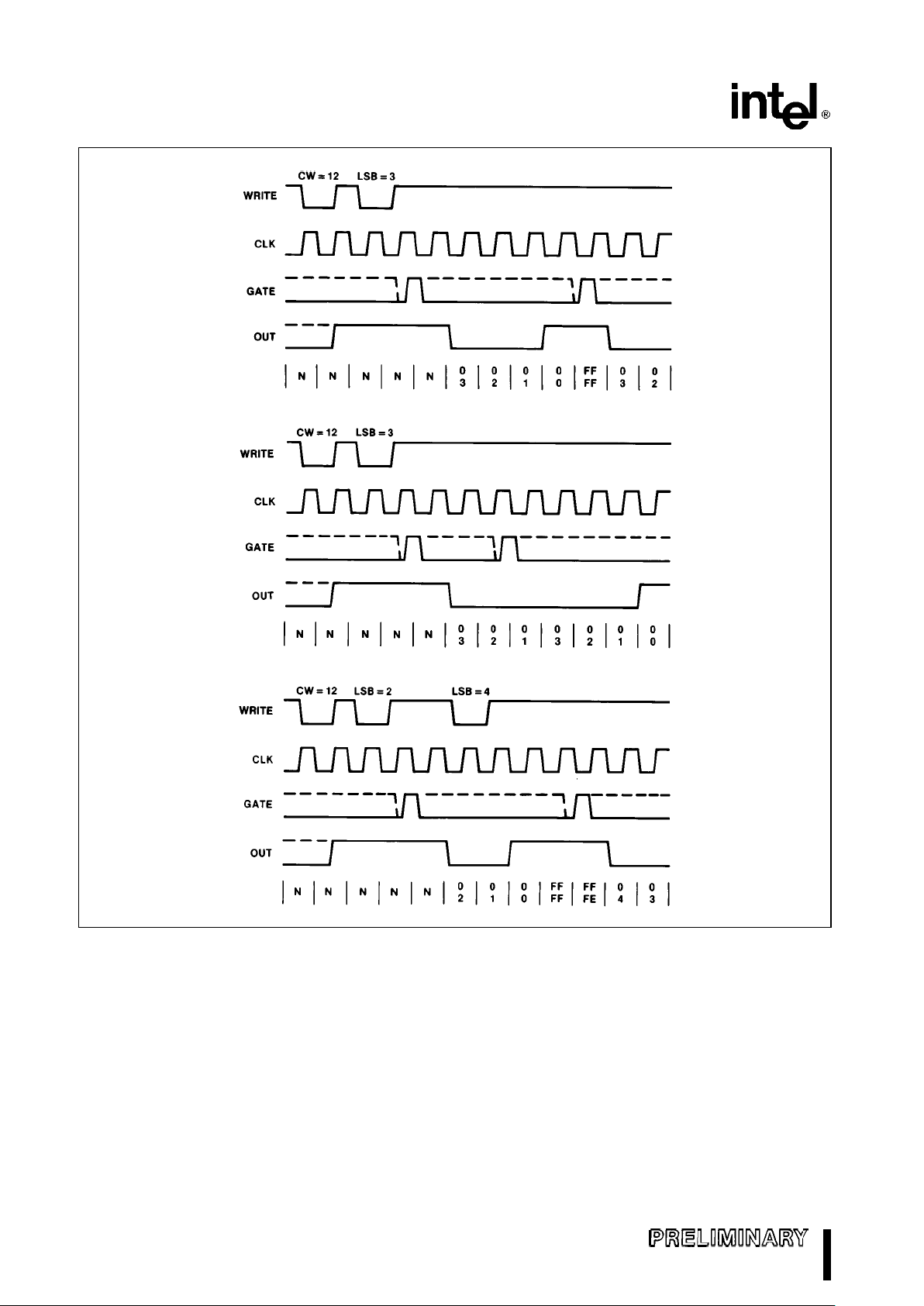
M82380
271070–71
Figure 44. Mode 1
5.3.3 MODE 2ÐRATE GENERATOR
This mode is a divide-by-N counter. It is typically
used to generate a Real Time Clock interrupt. OUT
will initially be HIGH. When the initial count has decremented to 1, OUT goes LOW for one CLK pulse,
then OUT goes HIGH again. Then the timer reloads
the initial count and the process is repeated. In other
words, this mode is periodic since the same sequence is repeated itself indefinitely. For an initial
count of N, the sequence repeats every N CLK cycles.
Similar to Mode 0, GATE
e
HIGH enables counting,
where GATE
e
LOW disables counting. If GATE
goes LOW during an output pulse (LOW), OUT is set
HIGH immediately. A trigger (rising edge on GATE)
will reload the timer with the initial count on the next
CLK pulse. Then, OUT will go LOW (for one CLK
pulse) N CLK pulses after the new trigger. Thus,
GATE can be used to synchronize the timer.
76
Page 77
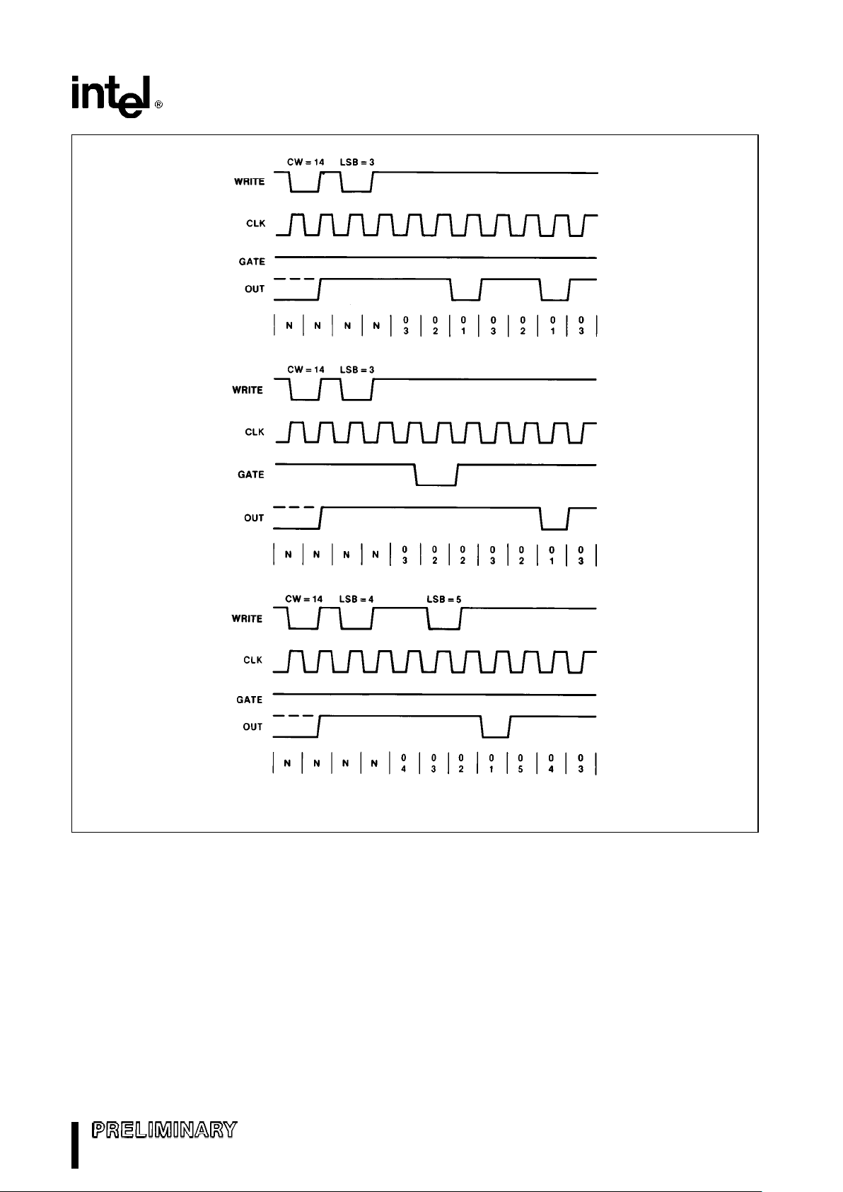
M82380
271070–72
NOTE:
A GATE transition should not occur one clock prior to terminal count.
Figure 45. Mode 2
After writing a Control Word and initial count, the
timer will be loaded on the next CLK pulse. OUT
goes LOW (for the CLK pulse) N CLK pulses after
the initial count is written. This is another way the
timer may be synchronized by software.
Writing a new count while counting does not affect
the current counting sequence because the new
count will not be loaded until the end of the current
counting cycle. If a trigger is received after writing a
new count but before the end of the current period,
the timer will be loaded with the new count on the
next CLK pulse after the trigger, and counting will
continue with the new count.
5.3.4 MODE 3ÐSQUARE WAVE GENERATOR
Mode 3 is typically used for Baud Rate generation.
Functionally, this mode is similar to Mode 2 except
for the duty cycle of OUT. In this mode, OUT will be
initially HIGH. When half of the initial count has expired, OUT goes low for the remainder of the count.
77
Page 78
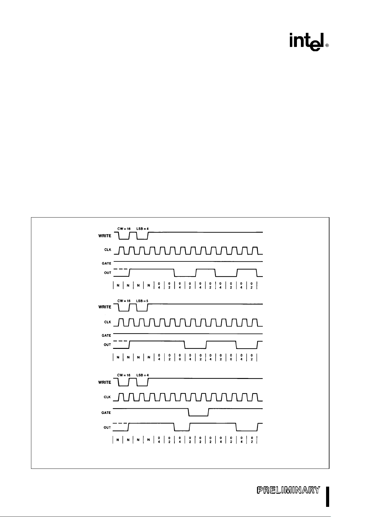
M82380
The counting sequence will be repeated, thus this
mode is also periodic. Note that an initial count of N
results in a square wave with a period of N CLK
pulses.
The GATE input can be used to synchronize the timer. GATE
e
HIGH enables counting; GATEeLOW
disables counting. If GATE goes LOW while OUT is
LOW, OUT is set HIGH immediately (i.e., no CLK
pulse is required). A trigger reloads the timer with the
initial count on the next CLK pulse.
After writing a Control Word and initial count, the
timer will be loaded on the next CLK pulse. This allows the timer to be synchronized by software.
Writing a new count while counting does not affect
the current counting sequence. If a trigger is received after writing a new count but before the end
of the current half-cycle of the square wave, the timer will be loaded with the new count on the next CLK
pulse and counting will continue from the new count.
Otherwise, the new count will be loaded at the end
of the current half-cycle.
There is a slight difference in operation depending
on whether the initial count is EVEN or ODD. The
following description is to show exactly how this
mode is implemented.
EVEN COUNTS:
OUT is initially HIGH. The initial count is loaded on
one CLK pulse and is decremented by two on succeeding CLK pulses. When the count expires (decremented to 2), OUT changes to LOW and the timer is
reloaded with the initial count. The above process is
repeated indefinitely.
ODD COUNTS:
OUT is initially HIGH. The initial count minus one
(which is an even number) is loaded on one CLK
271070–73
NOTE:
A-GATE transition should not occur one clock prior to terminal count.
Figure 46. Mode 3
78
Page 79
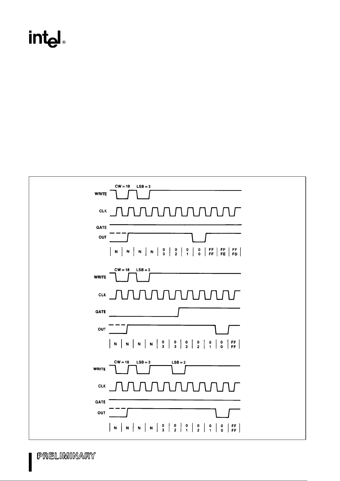
M82380
pulse and is decremented by two on succeeding
CLK pulses. One CLK pulse after the count expires
(decremented to 2), OUT goes LOW and the timer is
loaded with the initial count minus one again. Succeeding CLK pulses decrement the count by two.
When the count expires, OUT goes HIGH immediately and the timer is reloaded with the initial count
minus one. The above process is repeated indefinitely. So for ODD counts, OUT will be HIGH for (N
a
1)/2 counts and LOW for (Nb1)/2 counts.
5.3.5 MODE 4ÐINITIAL COUNT TRIGGERED
STROBE
This mode allows a strobe pulse to be generated by
writing an initial count to the timer. Initially, OUT will
be HIGH. When a new initial count is written into the
timer, the counting sequence will begin. When the
initial count expires (decremented to 1), OUT will go
LOW for one CLK pulse and then go HIGH again.
Again, GATE
e
HIGH enables counting while GATE
e
LOW disables counting. GATE has no effect on
OUT.
After writing the Control Word and initial count, the
timer will be loaded on the next CLK pulse. This CLK
pulse does not decrement the count, so for an initial
count of N, OUT does not strobe LOW until N
a
1
CLK pulses after initial count is written.
If a new count is written during counting, it will be
loaded in the next CLK pulse and counting will continue from the new count.
271070–74
Figure 47. Mode 4
79
Page 80
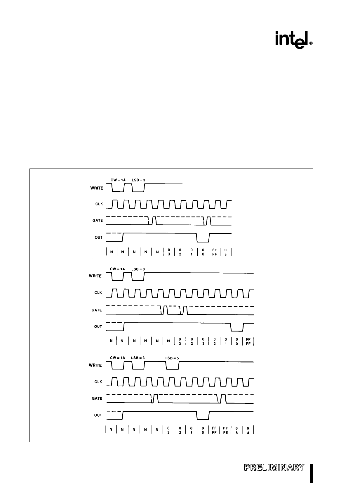
M82380
If a two-byte count is written, the following will occur:
1. Writing the first byte has no effect on counting.
2. Writing the second byte allows the new count to
be loaded on the next CLK pulse.
OUT will strobe LOW N
a
1 CLK pulses after the
new count of N is written. Therefore, when the
strobe pulse will occur after a trigger depends on the
value of the initial count loaded.
5.3.6 MODE 5ÐGATE RETRIGGERABLE
STROBE
Mode 5 is very similar to Mode 4 except the count
sequence is triggered by the GATE signal instead of
by writing an initial count. Initially, OUT will be HIGH.
Counting is triggered by a rising edge of GATE.
When the initial count has expired (decremented to
1), OUT will go LOW for one CLK pulse and then go
HIGH again.
After loading the Control Word and initial count, the
Count Element will not be loaded until the CLK pulse
after a trigger. This CLK pulse does not decrement
the count. Therefore, for an initial count of N, OUT
does not strobe LOW until N
a
1 CLK pulses after a
trigger.
271070–75
Figure 48. Mode 5
80
Page 81

M82380
SUMMARY OF GATE OPERATIONS
Mode
GATE LOW or
GATE Rising
GATE
Going LOW HIGH
0 Disable Count No Effect Enable Count
1 No Effect 1. Initiate Count No Effect
2. Reset Output
After Next Clock
2 1. Disable Count Initiate Count Enable Count
2. Sets Output HIGH
Immediately
3 1. Disable Count Initiate Count Enable Count
2. Sets Output HIGH
Immediately
4 Disable Count No Effect Enable Count
5 No Effect Initiate Count No Effect
The counting sequence is retriggerable. Every trigger will result in the timer being loaded with the initial
count on the next CLK pulse.
If the new count is written during counting, the current counting sequence will not be affected. If a trigger occurs after the new count is written but before
the current count expires, the timer will be loaded
with the new count on the next CLK pulse and a new
count sequence will start from there.
5.3.7 OPERATION COMMON TO ALL MODES
GATE
The GATE input is always sampled on the rising
edge of CLKIN. In Modes 0, 2, 3 and 4, the GATE
input is level sensitive. The logic level is sampled on
the rising edge of CLKIN. In Modes 1, 2, 3 and 5, the
GATE input is rising edge sensitive. In these modes,
a rising edge of GATE (trigger) sets an edge sensitive flip-flop in the timer. The flip-flop is reset immediately after it is sampled. This way, a trigger will be
detected no matter when it occurs; i.e., a HIGH logic
level does not have to be maintained until the next
rising edge of CLKIN. Note that in Modes 2 and 3,
the GATE input is both edge and level sensitive.
COUNTER
New counts are loaded and counters are decremented on the falling edge of CLKIN. The largest
possible initial count is 0. This is equivalent to 2**16
for binary counting and 10**4 for BCD counting.
Note that the counter does not stop when it reaches
zero. In Modes 0, 1, 4, and 5, the counter ‘wraps
around’ to the highest count: either FFFF Hex for
binary counting or 9999 for BCD counting, and continues counting. Modes 2 and 3 are periodic. The
counter reloads itself with the initial count and continues counting from there.
The minimum and maximum initial count in each
counter depends on the mode of operation. They
are summarized below.
Mode Min Max
010
110
220
320
410
510
5.4 Register Set Overview
The Programmable Interval Timer module of the
M82380 contains a set of six registers. The port address map of these registers is shown in Table 13.
Table 13. Timer Register Port Address Map
Port Address Description
40H Counter 0 Register (read/write)
41H Counter 1 Register (read/write)
42H Counter 2 Register (read/write)
43H Control Word Register I
(Counter 0,1&2)(write-only)
44H Counter 3 Register (read/write)
45H Reserved
46H Reserved
47H Control Word Register II
(Counter 3) (write-only)
81
Page 82

M82380
5.4.1 COUNTER 0, 1, 2, 3 REGISTERS
These four 8-bit registers are functionally identical.
They are used to write the initial count value into the
respective timer. Also, they can be used to read the
latched count value of a timer. Since they are 8-bit
registers, reading and writing of the 16-bit initial
count must follow the count format specified in the
Control Word Registers; i.e., least significant byte
only, most significant byte only, or least significant
byte then most significant byte (see Programming).
5.4.2 CONTROL WORD REGISTERI&II
There are two Control Word Registers associated
with the Timer section. One of the two registers
(Control Word Register I) is used to control the operations of Counters 0, 1, and 2 and the other (Control
Word Register II) is for Counter 3. The major functions of both Control Word Registers are listed below:
Ð Select the timer to be programmed.
Ð Define which mode the selected timer is to oper-
ate in.
Ð Define the count sequence; i.e., if the selected
timer is to count as a Binary Counter or a Binary
Coded Decimal (BCD) Counter.
Ð Select the byte access sequence during timer
read/write operations; i.e., least significant byte
only, most significant byte only, or least significant byte first, then most significant byte.
Also, the Control Word Registers can be programmed to perform a Counter Latch Command or a
Read Back Command which will be described later.
5.5 Programming
5.5.1 INITIALIZATION
Upon power-up or reset, the state of all timers is
undefined. The mode, count value, and output of all
timers are random. From this point on, how each
timer operates is determined solely by how it is programmed. Each timer must be programmed before it
can be used. Since the outputs of some timers can
generate interrupt signals to the M82380, all timers
should be initialized to a known state.
Timers are programmed by writing a Control Word
into their respective Control Word Registers. Then,
an Initial Count can be written into the correspond-
ing Count Register. In general, the programming procedure is very flexible. Only two conventions need to
be remembered:
1. For each timer, the Control Word must be written
before the initial count is written.
2. The 16-bit initial count must follow the count format specified in the Control Word (least significant byte only, most significant byte only, or least
significant byte first, followed by most significant
byte).
Since the two Control Word Registers and the four
Counter Registers have separate addresses, and
each timer can be individually selected by the appropriate Control Word Register, no special instruction
sequence is required. Any programming sequence
that follows the conventions above is acceptable.
A new initial count may be written to a timer at any
time without affecting the timer’s programmed mode
in any way. Count sequence will be affected as described in the Modes of Operation section. Note that
the new count must follow the programmed count
format.
If a timer is previously programmed to read/write
two-byte counts, the following precaution applies. A
program must not transfer control between writing
the first and second byte to another routine which
also writes into the same timer. Otherwise, the
read/write will result in incorrect count.
Whenever a Control Word is written to a timer, all
control logic for that timer(s) is immediately reset
(i.e., no CLK pulse is required). Also, the corresponding output pin, TOUT
), goes to a known initial
state.
5.5.2 READ OPERATION
Three methods are available to read the current
count as well as the status of each timer. They are:
Read Counter Registers, Counter Latch Command
and Read Back Command. Following is a description of these methods.
READ COUNTER REGISTERS
The current count of a timer can be read by performing a read operation on the corresponding Counter
Register. The only restriction of this read operation
is that the CLKIN of the timers must be inhibited by
82
Page 83

M82380
using external logic. Otherwise, the count may be in
the process of changing when it is read, giving an
undefined result. Note that since all four timers are
sharing the same CLKIN signal, inhibiting CLKIN to
read a timer will unavoidably disable the other timers
also. This may prove to be impractical. Therefore, it
is suggested that either the Counter Latch Command or the Read Back Command be used to read
the current count of a timer.
Another alternative is to temporarily disable a timer
before reading its Counter Register by using the
GATE input. Depending on the mode of operation,
GATE
e
LOW will disable the counting operation.
However, this option is available on Timer 2 and 3
only, since the GATE signals of the other two timers
are internally enabled all the time.
COUNTER LATCH COMMAND
A Counter Latch Command will be executed whenever a special Control Word is written into a Control
Word Register. Two bits written into the Control
Word Register distinguish this command from a ‘regular’ Control Word (see Register Bit Definition). Also,
two other bits in the Control Word will select which
counter is to be latched.
Upon execution of this command, the selected
counter’s Output Latch (OL) latches the count at the
time the Counter Latch Command is received. This
count is held in the latch until it is read by the
M80386, or until the timer is reprogrammed. The
count is then unlatched automatically and the OL
returns to ‘following’ the Counting Element (CE).
This allows reading the contents of the counters ‘on
the fly’ without affecting counting in progress. Multiple Counter Latch Commands may be used to latch
more than one counter. Each latched count is held
until it is read. Counter Latch Commands do not affect the programmed mode of the timer in any way.
If a counter is latched, and at some time later, it is
latched again before the prior latched count is read,
the second Counter Latch Command is ignored. The
count read will then be the count at the time the first
command was issued.
In any event, the latched count must be read according to the programmed format. Specifically, if
the timer is programmed for two-byte counts, two
bytes must be read. However, the two bytes do not
have to be read right after the other. Read/write or
programming operations of other timers may be performed between them.
Another feature of this Counter Latch Command is
that read and write operations of the same timer
may be interleaved. For example, if the timer is programmed for two-byte counts, the following sequence is valid.
1. Read least significant byte.
2. Write new least significant byte.
3. Read most significant byte.
4. Write new most significant byte.
If a timer is programmed to read/write two-byte
counts, the following precaution applies. A program
must not transfer control between reading the first
and second byte to another routine which also reads
from that same timer. Otherwise, an incorrect count
will be read.
READ BACK COMMAND
The Read Back Command is another special Command Word operation which allows the user to read
the current count value and/or the status of the selected timer(s). Like the Counter Latch Command,
two bits in the Command Word identify this as a
Read Back Command (see Register Bit Definition).
The Read Back Command may be used to latch
multiple counter Output Latches (OL’s) by selecting
more than one timer within a Command Word. This
single command is functionally equivalent to several
Counter Latch Commands, one for each counter to
be latched. Each counter’s latched count will be
held until it is read by the M80386 or until the timer is
reprogrammed. The counter is automatically unlatched when read, but other counters remain
latched until they are read. If multiple Read Back
commands are issued to the same timer without
reading the count, all but the first are ignored; i.e.,
the count read will correspond to the very first Read
Back Command issued.
As mentioned previously, the Read Back Command
may also be used to latch status information of the
selected timer(s). When this function is enabled, the
status of a timer can be read from the Counter Register after the Read Back Command is issued. The
status information of a timer includes the following:
1. Mode of timer:
This allows the user to check the mode of operation of the timer last programmed.
2. State of TOUT pin of the timer:
This allows the user to monitor the counter’s output pin via software, possibly eliminating some
hardware from a system.
83
Page 84
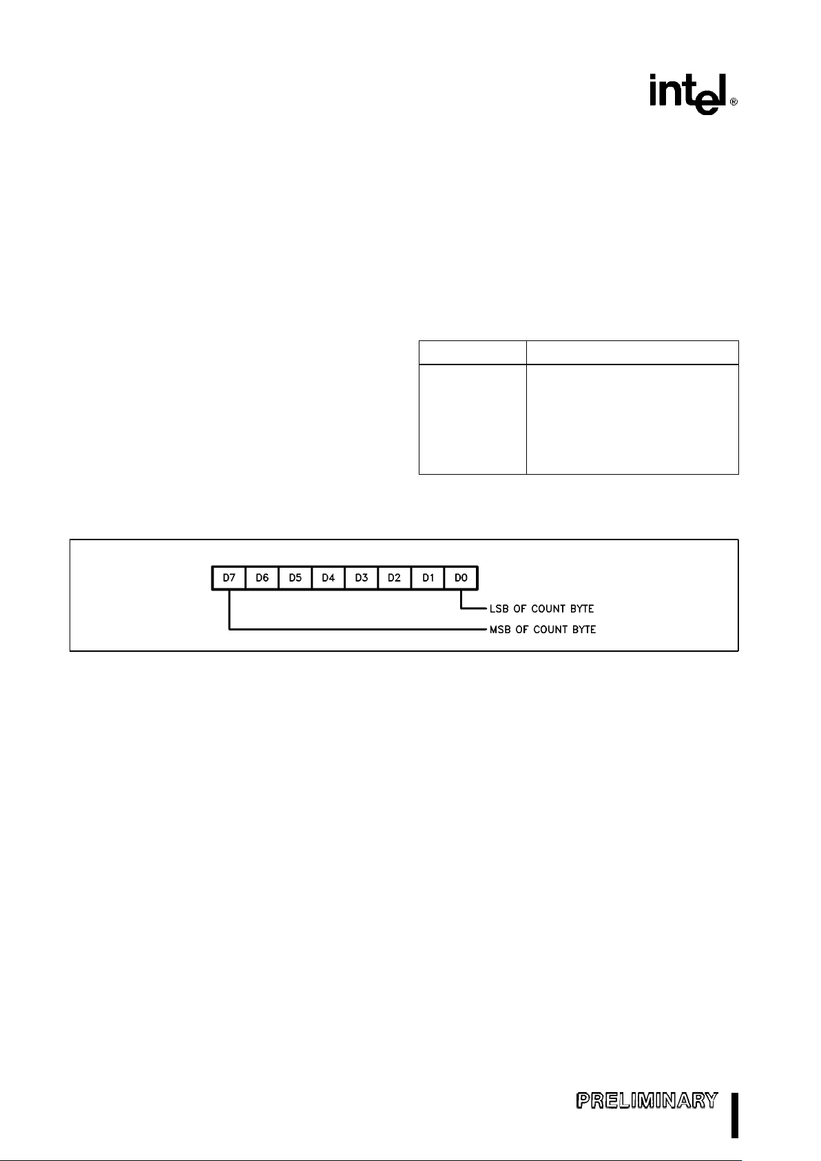
M82380
3. Null Count/Count available:
The Null Count Bit in the status byte indicates if
the last count written to the Count Register (CR)
has been loaded into the Counting Element (CE).
The exact time this happens depends on the
mode of the timer and is described in the Programming section. Until the count is loaded into
the Counting Element (CE), it cannot be read from
the timer. If the count is latched or read before
this occurs, the count value will not reflect the
new count just written.
If multiple status latch operations of the timer(s) are
performed without reading the status, all but the first
command are ignored; i.e., the status read in will
correspond to the first Read Back Command issued.
Both the current count and status of the selected
timer(s) may be latched simultaneously by enabling
both functions in a single Read Back Command.
This is functionally the same as issuing two separate
Read Back Commands at once. Once again, if multiple read commands are issued to latch both the
count and status of a timer, all but the first command
will be ignored.
If both count and status of a timer are latched, the
first read operation of that timer will return the
latched status, regardless of which was latched first.
The next one or two (if two count bytes are to be
read) read operations return the latched count. Note
that subsequent read operations on the Counter
Register will return the unlatched count (like the first
read method discussed).
5.6 Register Bit Definitions
COUNTER 0, 1, 2, 3 REGISTER (READ/WRITE)
Port Address Description
40H Counter 0 Register (read/write)
41H Counter 1 Register (read/write)
42H Counter 2 Register (read/write)
44H Counter 3 Register (read/write)
45H Reserved
46H Reserved
271070–76
84
Page 85
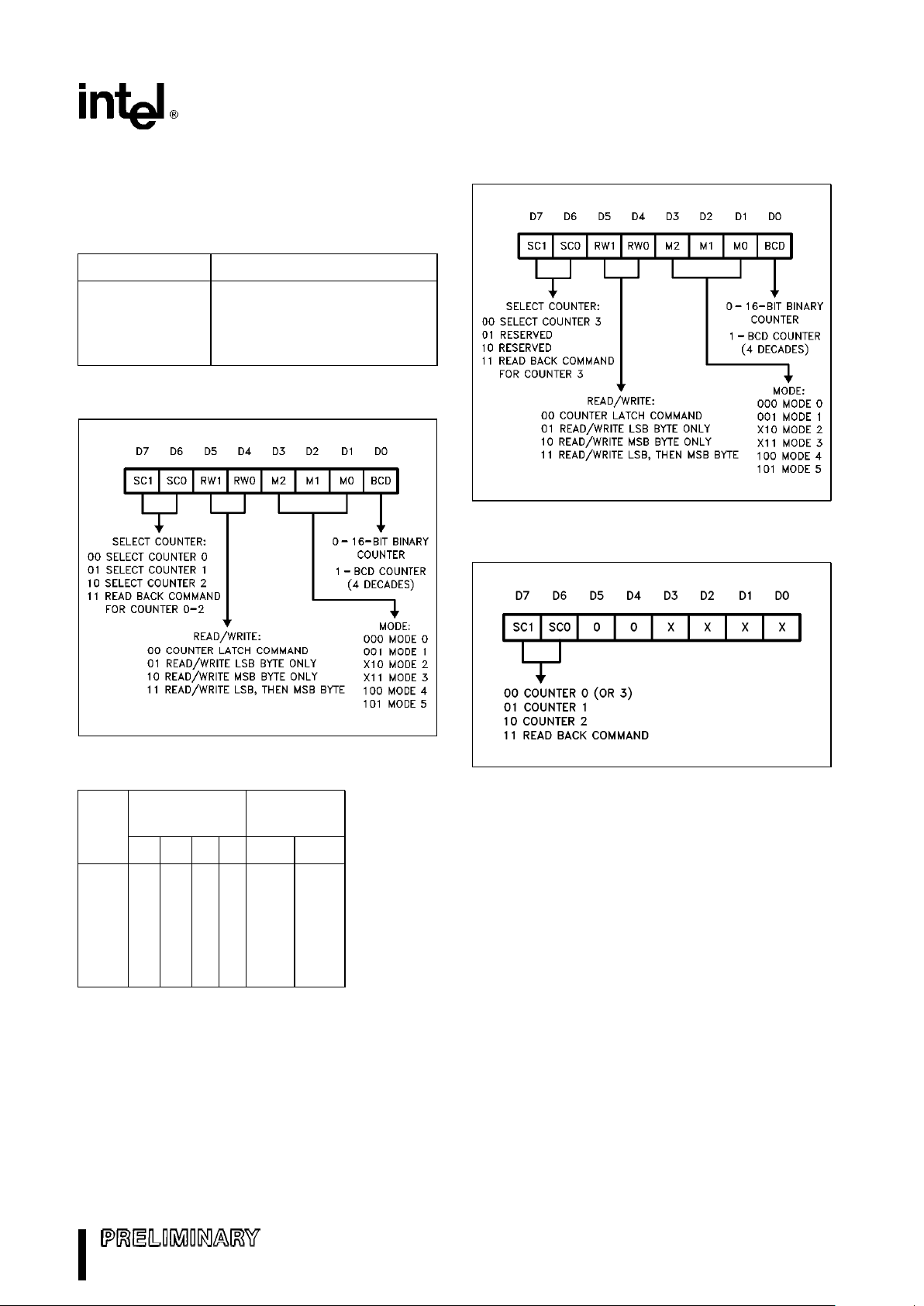
M82380
Note that these 8-bit registers are for writing and
reading of one byte of the 16-bit count value, either
the most significant or the least significant byte.
CONTROL WORD REGISTER I & II (WRITE-ONLY)
Port Address Description
43H Control Word Register I
(Counter 0, 1, 2) (write-only)
47H Control Word Register II
(Counter 3) (write-only)
CONTROL WORD REGISTER I
271070–77
CONTROL WORD REGISTER II
271070–78
COUNTER LATCH COMMAND FORMAT
(Write to Control Word Register)
271070–79
Timer
Gate
Mode Trigger
0 1 2 3 Edge Level
0 X Interrupt on Terminal Count
1NANA
jj X Gate Retriggerable One Shot
2 X X Rate Generator
3 X X Square Wave Generator
4 X Initial Count Triggered Strobe
5NANAjj X Gate Retriggerable Strobe
j
e
Must use Port 61 to generate L edge.
NA
e
Not Applicable
85
Page 86

M82380
READ BACK COMMAND FORMAT
(Write to Control Word Register)
271070–80
STATUS FORMAT
(Returned from Read Back Command)
271070–81
6.0 WAIT STATE GENERATOR
6.1 Functional Description
The M82380 contains a programmable Wait State
Generator which can generate a pre-programmed
number of wait states during both CPU and DMA
initiated bus cycles. This Wait State Generator is capable of generating 1 to 16 wait states in non-pipelined mode, and 0 to 15 wait states in pipelined
mode. Depending on the bus cycle type and the two
Wait State Control inputs (WSC 0 – 1), a pre-programmed number of wait states in the selected Wait
State Register will be generated.
The Wait State Generator can also be disabled to
allow the use of devices capable of generating their
own READY
signals. Figure 49 is a block diagram of
the Wait State Generator.
86
Page 87
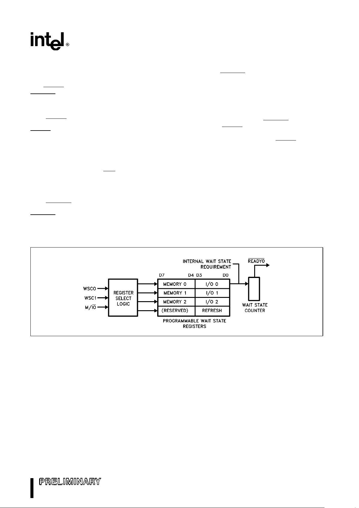
M82380
6.2 Interface Signals
The following describes the interface signals which
affect the operation of the Wait State Generator.
The READY
, WSC0 and WSC1 signals are inputs.
READYO
is the ready output signal to the host proc-
essor.
6.2.1 READY
READY is an active LOW input signal which indicates to the M82380 the completion of a bus cycle.
In the Master mode (e.g., M82380 initiated DMA
transfer), this signal is monitored to determine
whether a peripheral or memory needs wait states
inserted in the current bus cycle. In the Slave mode,
it is used (together with the ADS
signal) to trace CPU
bus cycles to determine if the current cycle is pipelined.
6.2.2 READYO
READYO (Ready Out) is an active LOW output signal and is the output of the Wait State Generator.
The number of wait states generated depends on
the WSC(0– 1) inputs. Note that special cases are
handled for access to the M82380 internal registers
and for the Refresh cycles. For M82380 internal register access, READYO
will be delayed to take into
account the command recovery time of the register.
One or more wait states will be generated in a pipelined cycle. During refresh, the number of wait states
will be determined by the preprogrammed value in
the Refresh Wait State Register.
In the simplest configuration, READYO
can be con-
nected to the READY
input of the M82380 and the
i386 CPU. This is, however, not always the case. If
external circuitry is to control the READY
inputs as
well, additional logic will be required (see Application
Issues).
6.2.3 WSC(0 –1)
These two Wait State Control inputs select one of
the three pre-programmed 8-bit Wait State Registers
which determines the number of wait states to be
generated. The most significant half of the three
Wait State Registers corresponds to memory accesses, the least significant half to I/O accesses.
The combination WSC(0–1)
e
11 disables the Wait
State Generator.
271070–82
Figure 49. Wait State Generator Block Diagram
87
Page 88
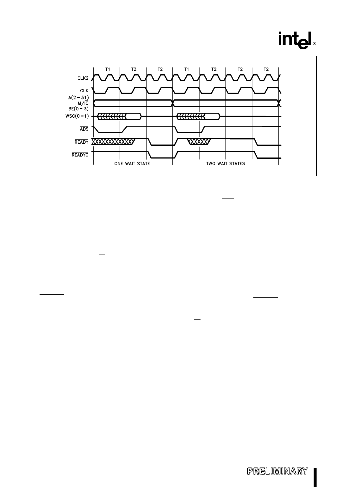
M82380
271070–83
Figure 50. Wait States in Non-Pipelined Cycles
6.3 Bus Function
6.3.1 WAIT STATES IN NON-PIPELINED CYCLE
The timing diagram of two typical non-pipelined cycles with M82380 generated wait states is shown in
Figure 50. In this diagram, it is assumed that the
internal registers of the M82380 are not addressed.
During the first T2 state of each bus cycle, the Wait
State Control and the M/IO
inputs are sampled to
determine which Wait State Register (if any) is selected. If the WSC inputs are active (i.e., not both are
driven HIGH), the pre-programmed number of wait
states corresponding to the selected Wait State
Register will be requested. This is done by driving
the READYO
output HIGH during the end of each T2
state.
The WSC(0 – 1) inputs need only be valid during the
very first T2 state of each non-pipelined cycle. As a
general rule, the WSC inputs are sampled on the
rising edge of the next clock (M82384 CLK) after the
last state when ADS
(Address Status) is asserted.
The number of wait states generated depends on
the type of bus cycle, and the number of wait states
requested. The various combinations are discussed
below.
1. Access the M82380 internal registers: 2 to 5 wait
states, depending upon the specific register addressed. Some back-to-back sequences to the Interrupt Controller will require 7 wait states.
2. Interrupt Acknowledge to the M82380: 5 wait
states.
3. Refresh: As programmed in the Refresh Wait
State Register (see Register Set Overview). Note
that if WSC(0 –1)
e
11, READYO will stay inac-
tive.
4. Other bus cycles: Depending on WSC(0– 1) and
M/IO
inputs, these inputs select a Wait State
Register in which the number of wait states will be
equal to the pre-programmed wait state count in
the register plus 1. The Wait State Register selection is defined as follows (Table 14).
88
Page 89
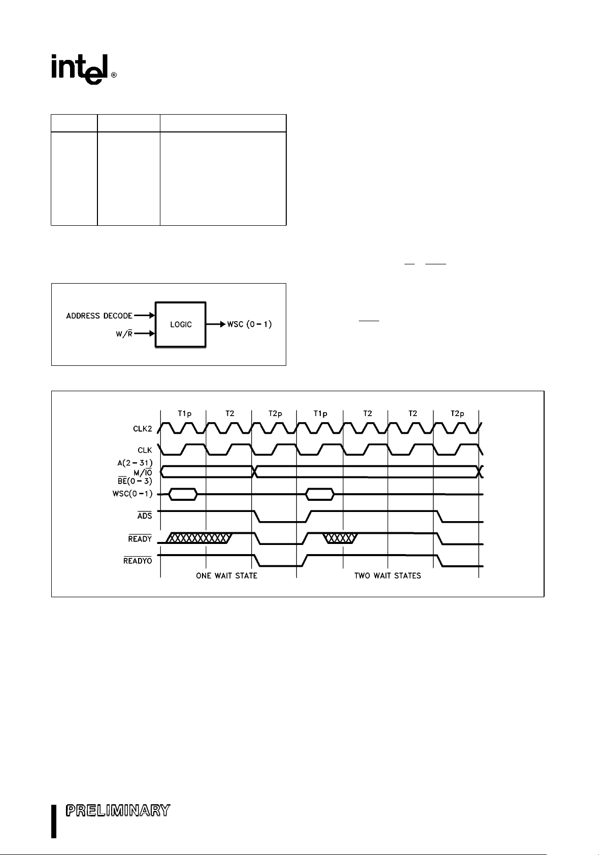
M82380
Table 14. Wait State Register Selection
M/IO
Ý
WSC(1– 0) Register Selected
0 00 WAIT REG 0 (I/O half)
0 01 WAIT REG 1 (I/O half)
0 10 WAIT REG 2 (I/O half)
1 00 WAIT REG 0 (MEM half)
1 01 WAIT REG 1 (MEM half)
1 10 WAIT REG 2 (MEM half)
X 11 Wait State Gen. Disabled
The Wait State Control signals, WSC(0– 1), can be
generated with the address decode and the Read/
Write control signals as shown in Figure 51.
271070–84
Figure 51. WSC(0– 1) Generation
Note that during HALT and SHUTDOWN, the number of wait states will depend on the WSC(0– 1) inputs, which will select the memory half of one of the
Wait State Registers (see CPU Reset and Shutdown
Detect).
6.3.2 WAIT STATES IN PIPELINED CYCLE
The timing diagram of two typical pipelined cycles
with M82380 generated wait states is shown in Figure 52. Again, in this diagram, it is assumed that the
M82380 internal registers are not addressed. As defined in the timing of the i386 processor, the Address (A 2 –31), Byte Enable (BE 0– 3), and other
control signals (M/IO
, ADS) are asserted one
T state earlier than in a non-pipelined cycle; i.e., they
are asserted at T2P. Similar to the non-pipelined
case, the Wait State Control (WSC) inputs are sampled in the middle of the state after the last state
when the ADS
signal is asserted. Therefore, the
WSC inputs should be asserted during the T1P state
of each pipelined cycle (which is one T state earlier
than in the non-pipelined cycle).
271070–85
Figure 52. Wait State in Pipelined Cycles
89
Page 90

M82380
The number of wait states generated in a pipelined
cycle is selected in a similar manner as in the nonpipelined case discussed in the previous section.
The only difference here is that the actual number of
wait states generated will be one less than that of
the non-pipelined cycle. This is done automatically
by the Wait State Generator.
6.3.3 EXTENDING AND EARLY TERMINATING
BUS CYCLE
The M82380 allows external logic to either add wait
states or cause early termination of a bus cycle by
controlling the READY
input to the M82380 and the
host processor. A possible configuration is shown in
Figure 53.
The EXTERNAL READY
signal of Figure 53 allows
external devices to cause early termination of a bus
cycle. When this signal is asserted LOW, the output
of the circuit will also go LOW (even though the
READYO of the M82380 may still be HIGH). This
output is fed to the READY
input of the M80386 and
the M82380 to indicate the completion of the current
bus cycle.
Similarly, the EXT. NOT READY (External Not
Ready) signal is used to delay the READY
input of
the processor and the M82380. As long as this signal is driven HIGH, the output of the circuit will drive
the READY
input HIGH. This will effectively extend
the duration of a bus cycle. However, it is important
to note that if the two-level logic is not fast enough
to satisfy the READY
setup time, the OR gate should
be eliminated. Instead, the M82380 Wait State Generator can be disabled by driving both WSC(0 – 1)
HIGH. In this case, the addressed memory or I/O
device should activate the external READY
input
whenever it is ready to terminate the current bus
cycle.
Figure 54 and 55 show the timing relationships of
the ready signals for the early termination and extension of the bus cycles. The Application Issues section of this data sheet contains a detailed timing
analysis of the external circuit.
271070–86
Figure 53. External ‘READY’ Control Logic
271070–87
Figure 54. Early Termination of Bus Cycle by ‘READY’
90
Page 91

M82380
271070–88
Figure 55. Extending Bus Cycle by ‘READY’
Due to the following implications, it should be noted
that early termination of bus cycles in which M82380
internal registers are accessed is not recommended.
1. Erroneous data may be read from or written into
the addressed register.
2. The M82380 must be allowed to recover either
before HLDA (Hold Acknowledge) is asserted or
before another bus cycle into an M82380 internal
register is initiated.
The recovery time, in bus periods, equals the remaining wait states that were avoided plus 4.
6.4 Register Set Overview
Altogether, there are four 8-bit internal registers associated with the Wait State Generator. The port address map of these registers is shown below in Table 15. A detailed description of each follows.
Table 15. Register Address Map
Port Address Description
72H Wait State Reg 0 (read/write)
73H Wait State Reg 1 (read/write)
74H Wait State Reg 2 (read/write)
75H Ref. Wait State Reg (read/write)
WAIT STATE REGISTER 0, 1, 2
These three 8-bit read/write registers are functionally identical. They are used to store the pre-programmed wait state count. One half of each register
contains the wait state count for I/O accesses while
the other half contains the count for memory accesses. The total number of wait states generated
will depend on the type of bus cycle. For a non-pipelined cycle, the actual number of wait states requested is equal to the wait state count plus 1. For a
pipelined cycle, the number of wait states will be
equal to the wait state count in the selected register.
Therefore, the Wait State Generator is capable of
generating 1 to 16 wait states in non-pipelined
mode, and 0 to 15 wait states in pipelined mode.
Note that the minimum wait state count in each register is 0. This is equivalent to 0 wait states for a
pipelined cycle and 1 wait state for a non-pipelined
cycle.
REFRESH WAIT STATE REGISTER
Similar to the Wait State Registers discussed above,
this 4-bit register is used to store the number of wait
states to be generated during the DRAM refresh cycle. Note that the Refresh Wait State Register is not
selected by the WSC inputs. It will automatically be
91
Page 92
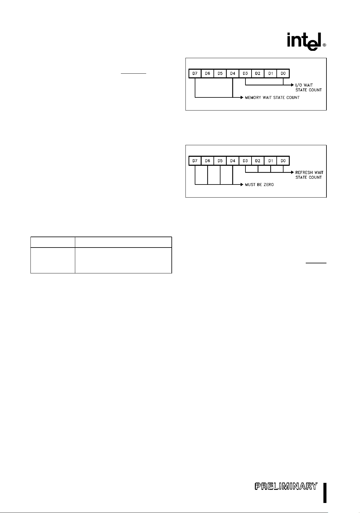
M82380
chosen whenever a DRAM refresh cycle occurs. If
the Wait State Generator is disabled during the refresh cycle (WSC(0 –1)
e
11), READYO will stay
inactive and the Refresh Wait State Register is ignored.
6.5 Programming
Using the Wait State Generator is relatively straightforward. No special programming sequence is required. In order to ensure the expected number of
wait states will be generated when a register is selected, the registers to be used must be programmed after power-up by writing the appropriate
wait state count into each register. Note that upon
hardware reset, all Wait State Registers are initialized with the value FFH, giving the maximum number of wait states possible. Also, each register can
be read to check the wait state count previously
stored in the register.
6.6 Register Bit Definition
WAIT STATE REGISTER 0, 1, 2
Port Address Description
72H Wait State Register 0 (read/write)
73H Wait State Register 1 (read/write)
74H Wait State Register 2 (read/write)
271070–89
REFRESH WAIT STATE REGISTER
Port Address: 75H (Read/Write)
271070–90
6.7 Application Issues
6.7.1 EXTERNAL ‘READY’ CONTROL LOGIC
As mentioned previously, wait state cycles generated by the M82380 can be terminated early or extended longer by means of additional external logic
(see Figure 53). In order to ensure that the READY
input timing requirement of the i386 processor and
the M82380 is satisfied, special care must be taken
when designing this external control logic. This section addresses the design requirements.
92
Page 93

M82380
A simplified block diagram of the external logic along
with the READY
timing diagram is shown in Figure
56. The purpose is to determine the maximum delay
time allowed in the external control logic in order to
satisfy the READY
setup time.
First, it will be assumed that the i386 processor is
running at 16 MHz (i.e., CLK2 and 32 MHz). Therefore, one bus state (two CLK2 periods) will be equivalent to 62.5 nsec. According to the AC specifica-
tions of the M82380, the maximum delay time for
valid READYO
signal is 31 ns after the rising edge of
CLK2 in the beginning of T2 (for non-pipelined cycle)
or T2P (for pipelined cycle). Also, the minimum
READY
setup time of the i386 processor and the
M82380 should be 20 ns before the rising edge of
CLK2 at the beginning of the next bus state. This
limits the total delay time for the external READY
control logic to be 11 ns (62.5b31b21) in order
to meet the READY
setup timing requirement.
271070–91
A
e
PHI1aPHI2e62.5 ns
B
e
Maximum READYO Valid Delaye31 ns
CeREADY Setup Timee21 ns
D
e
Maximum Ready Control Logic DelayeAbBbCe11 ns
Figure 56. ‘READY’ Timing Consideration
93
Page 94
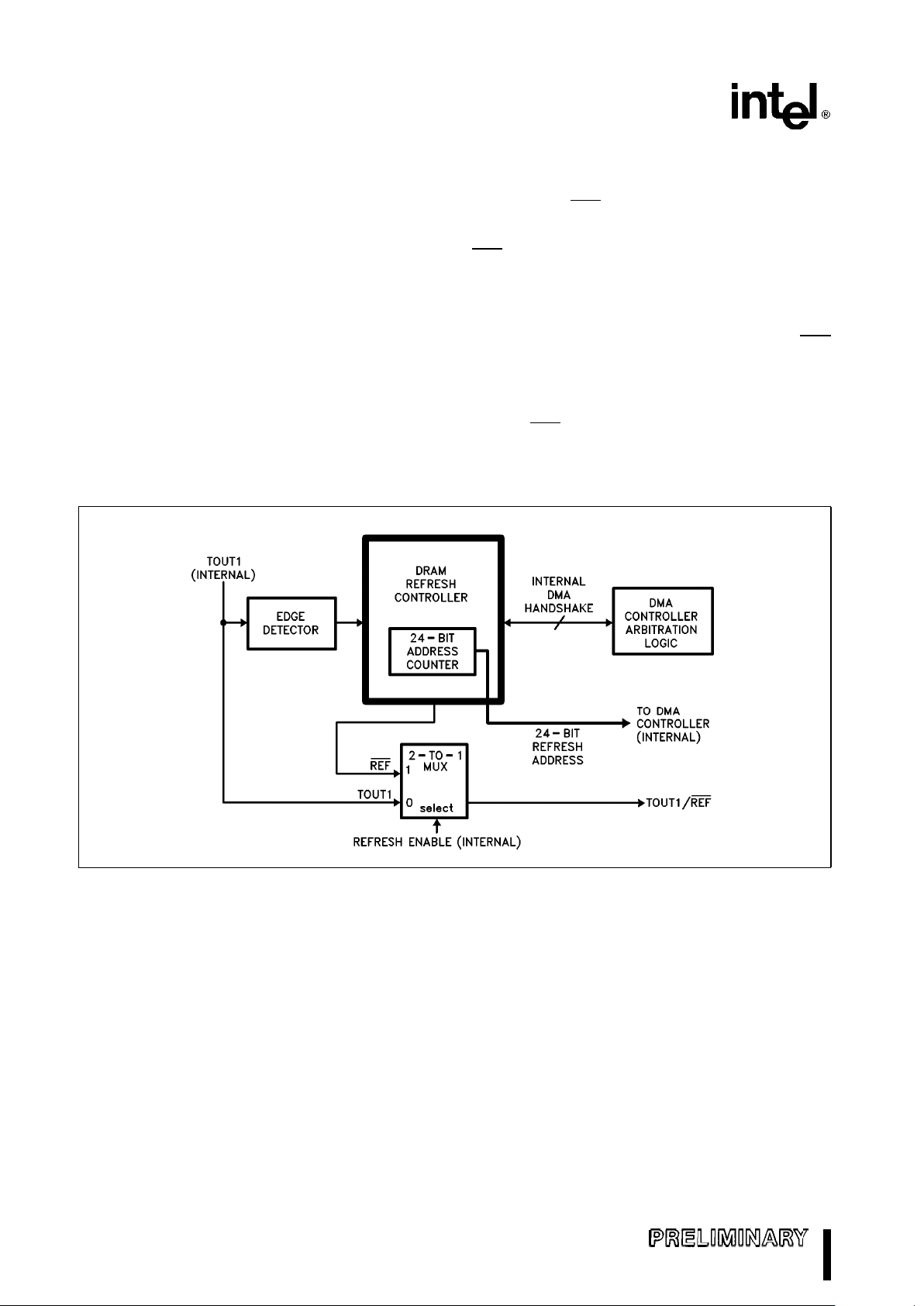
M82380
7.0 DRAM REFRESH CONTROLLER
7.1 Functional Description
The M82380 DRAM Refresh Controller consists of a
24-bit Refresh Address Counter and Refresh Request logic for DRAM refresh operations (see Figure
57). TIMER 1 can be used as a trigger signal to the
DRAM Refresh Request logic. The Refresh Bus Size
can be programmed to be 8-, 16-, or 32-bit wide.
Depending on the Refresh Bus Size, the Refresh
Address Counter will be incremented with the appropriate value after every refresh cycle. The internal
logic of the M82380 will give the Refresh operation
the highest priority in the bus control arbitration process. Bus control is not released and re-requested if
the M82380 is already a bus master.
7.2 Interface Signals
7.2.1 TOUT1/REF
The dual function output pin of TIMER 1 (TOUT1/
REF
) can be programmed to generate DRAM Refresh signal. If this feature is enabled, the rising edge
of TIMER 1 output (TOUT1) will trigger the DRAM
Refresh Request logic. After some delay for gaining
access of the bus, the M82380 DRAM Controller will
generate a DRAM Refresh signal by driving REF
output LOW. This signal is cleared after the refresh
cycle has taken place, or by a hardware reset.
If the DRAM Refresh feature is disabled, the
TOUT1/REF output pin is simply the TIMER 1 output. Detailed information of how TIMER 1 operates
is discussed in section 6ÐProgrammable Interval
Timer, and will not be repeated here.
271070–92
Figure 57. DRAM Refresh Controller
94
Page 95

M82380
7.3 Bus Function
7.3.1 ARBITRATION
In order to ensure data integrity of the DRAMs, the
M82380 gives the DRAM Refresh signal the highest
priority in the arbitration logic. It allows DRAM Refresh to interrupt a DMA in progress in order to perform the DRAM Refresh cycle. The DMA service will
be resumed after the refresh is done.
In case of a DRAM Refresh during a DMA process,
the cascaded device will be requested to get off the
bus. This is done by deasserting the EDACK signal.
Once DREQn goes inactive, the M82380 will perform the refresh operation. Note that the DMA controller does not completely relinquish the system bus
during refresh. The Refresh Generator simply
‘steals’ a bus cycle between DMA accesses.
Figure 58 shows the timing diagram of a Refresh
Cycle. Upon expiration of TIMER 1, the M82380 will
try to take control of the system bus by asserting
HOLD. As soon as the M82380 see HLDA go active,
the DRAM Refresh Cycle will be carried out by activating the REF
signal as well as the refresh address
and control signals on the system bus (Note that
REF
will not be active until two CLK periods after
HLDA is asserted). The address bus will contain the
24-bit address currently in the Refresh Address
Counter. The control signals are driven the same
way as in a Memory Read cycle. This ‘read’ operation is complete when the READY
signal is driven
LOW. Then, the M82380 will relinquish the bus by
de-asserting HOLD. Typically, a Refresh Cycle without wait states will take five bus states to execute. If
‘n’ wait states are added, the Refresh Cycle will last
for five plus ‘n’ bus states.
How often the Refresh Generation will initiate a refresh cycle depends on the frequency of CLKIN as
well as TIMER1’s programmed mode of operation.
For this specific application, TIMER1 should be programmed to operate in Mode 2 or 3 to generate a
constant clock rate. See the section titled Programmable Interval Timer for more information on programming the timer. One DRAM Refresh Cycle will
be generated each time TIMER 1 expires (when
TOUT1 changes to LOW to HIGH).
The Wait State Generator can be used to insert wait
states during a refresh cycle. The M82380 will automatically insert the desired number of wait states as
programmed in the Refresh Wait State Register (see
Wait State Generator).
7.4 Modes of Operation
7.4.1 WORD SIZE AND REFRESH
ADDRESS COUNTER
The M82380 supports 8-, 16- and 32-bit refresh cycle. The bus width during a refresh cycle is programmable (see Programming). The bus size can be programmed via the Refresh Control Register (see Register Overview). If the DRAM bus size is 8-, 16-, or
271070–93
*NOTE:
A24–A31
e
1 during Refresh cycle.
Figure 58. M82380 Refresh Cycle
95
Page 96
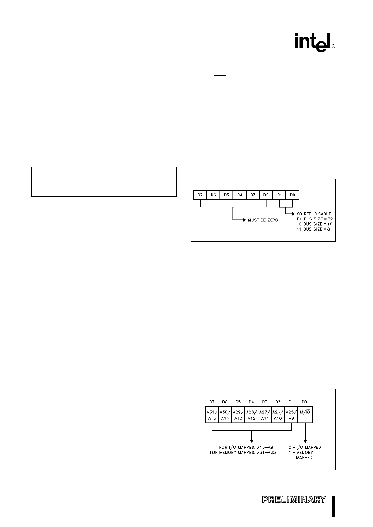
M82380
32-bits, the Refresh Address Counter will be incremented by 1, 2, or 4, respectively.
The Refresh Address Counter is cleared by a hardware reset.
7.5 Register Set Overview
The Refresh Generator has two internal registers to
control its operation. They are the Refresh Control
Register and the Refresh Wait State Register. Their
port address map is shown in Table 16 below.
Table 16. Register Address Map
Port Address Description
1CH Refresh Control Reg. (read/write)
75H Ref. Wait State Reg. (read/write)
The Refresh Wait State Register is not part of the
Refresh Generator. It is only used to program the
number of wait states to be inserted during a refresh
cycle. This register is discussed in detail in section 7
(Wait State Generator) and will not be repeated
here.
REFRESH CONTROL REGISTER
This 2-bit register serves two functions. First, it is
used to enable/disable the DRAM Refresh function
output. If disabled, the output of TIMER 1 is simply
used as a general purpose timer. The second function of this register is to program the DRAM bus size
for the refresh operation. The programmed bus size
also determines how the Refresh Address Counter
will be incremented after each refresh operation.
7.6 Programming
Upon hardware reset, the DRAM Refresh function is
disabled (the Refresh Control Register is cleared).
The following programming steps are needed before
the Refresh Generator can be used. Since the rate
of refresh cycles depends on how TIMER 1 is programmed, this timer must be initialized with the desired mode of operation as well as the correct refresh interval (see Programming Interval Timer).
Whether or not wait states are to be generated during a refresh cycle, the Refresh Wait State Register
must also be programmed with the appropriate value. Then, the DRAM Refresh feature must be enabled and the DRAM bus width should be defined.
These can be done in one step by writing the appropriate control word into the Refresh Control Register
(see Register Bit Definition). After these steps are
done, the refresh operation will automatically be invoked by the Refresh Generator upon expiration of
Timer 1.
In addition to the above programming steps, it
should be noted that after reset, although the
TOUT1/REF
becomes the Timer 1 output, the state
of this pin is undefined. This is because the Timer
module has not been initialized yet. Therefore, if this
output is used as a DRAM Refresh signal, this pin
should be disqualified by external logic until the Refresh function is enabled. One simple solution is to
logically AND this output with HLDA, since HLDA
should not be active after reset.
7.7 Register Bit Definition
REFRESH CONTROL REGISTER
Port Address: 1CH (Read/Write)
271070–94
8.0 RELOCATION REGISTER AND
ADDRESS DECODE
8.1 Relocation Register
All the integrated peripheral devices in the M82380
are controlled by a set of internal registers. These
registers span a total of 256 consecutive address
locations (although not all the 256 locations are
used). The M82380 provides a Relocation Register
which allows the user to map this set of internal registers into either the memory or I/O address space.
The function of the Relocation Register is to define
the base address of the internal register set of the
M82380 as well as if the registers are to be memoryor I/O-mapped. The format of the Relocation Register is depicted in Figure 59.
271070–95
Figure 59. Relocation Register
96
Page 97

M82380
Note that the Relocation Register is part of the internal register set of the M82380. It has a port address
of 7FH. Therefore, any time the content of the Relocation Register is changed, the physical location of
this register will also be moved. Upon reset of the
M82380, the content of the Relocation Register will
be cleared. This implies that the M82380 will respond to its I/O addresses in the range of 0000H to
00FFH.
8.1.1 I/O-MAPPED M82380
As shown in Figure 59, Bit 0 of the Relocation Register determines whether the M82380 registers are to
be memory-mapped or I/O-mapped. When Bit 0 is
set to ‘0’, the M82380 will respond to I/O Addresses. Address signals BE0
–BE3, A2– A7 will be used
to select one of the internal registers to be accessed. Bit 1 to Bit 7 of the Relocation Register will
correspond to A9 to A15 of the Address bus, respectively. Together with A8 implied to be ‘0’, A15 to A8
will be fully decoded by the M82380. The following
shows how the M82380 is mapped into the I/O address space.
Example
Relocation Register
e
11001110 (0CEH)
M82380 will respond to I/O address range
from 0CE00H to 0CEFFH.
Therefore, this I/O mapping mechanism allows the
M82380 internal registers to be located on any even,
contiguous, 256 byte boundary of the system I/O
space.
Port Address: 7FH (Read/Write)
8.1.2 MEMORY-MAPPED M82380
When Bit 0 of the Relocation Register is set to ‘1’,
the M82380 will respond to memory addresses.
Again, Address signals BE0
–BE3, A2 –A7 will be
used to select one of the internal registers to be
accessed. Bit 1 to Bit 7 of the Relocation Register
will correspond to A25 – A31, respectively. A24 is assumed to be ‘0’, and A8– A23 are ignored. Consider
the following example.
Example
Relocation Register
e
10100111 (0A7H)
The M82380 will respond to memory addresses
in the range of 0A6XXXX00H to 0A6XXXXFFH
(where ‘X’ is don’t care).
This scheme implies that the internal register can be
located in any even, contiguous, 2**24 byte page of
the memory space.
8.2 Address Decoding
As mentioned previously, the M82380 internal registers do not occupy the entire contiguous 256 address locations. Some of the locations are ‘unoccupied’. The M82380 always decodes the lower 8 address bits (A0 – A7) to determine if any one of its
registers is being accessed. If the address does not
correspond to any of its registers, the M82380 will
not respond. This allows external devices to be located within the ‘holes’ in the M82380 address
space. Note that there are several unused addresses reserved for future Intel peripheral devices.
9.0 CPU RESET AND SHUTDOWN
DETECT
The M82380 will activate the CPURST signal to reset the host processor when one of the following
conditions occurs:
Ð M82380 RESET is active;
Ð M82380 detects a i386 processor Shutdown cy-
cle (this feature can be disabled);
Ð CPURST software command is issued to i386
processor.
Whenever the CPURST signal is activated, the
M82380 will reset its own internal Slave-Bus state
machine.
9.1 Hardware Reset
Following a hardware reset, the M82380 will assert
its CPURST output to reset the host processor. This
output will stay active for as long as the RESET input
is active. During a hardware reset, the M82380 internal registers will be initialized as defined in the corresponding functional descriptions.
9.2 Software Reset
CPURST can be generated by writing the following
bit pattern into M82380 register location 64H.
D7 D0
1111XXX0
X
e
Don’t Care
97
Page 98

M82380
The Write operation into this port is considered as
an M82380 access and the internal Wait State Generator will automatically determine the required number of wait states. The CPURST will be active following the completion of the Write cycle to this port.
This signal will last for 62 CLK2 periods. The
M82380 should not be accessed until the CPURST
is deactivated.
This internal port is Write-Only and the M82380 will
not respond to a Read operation to this location.
Also, during a CPU software reset command, the
M82380 will reset its Slave-Bus state machine. However, its internal registers remain unchanged. This
allows the operating system to distinguish a ‘warm’
reset by reading any M82380 internal register previously programmed for an non-default value. The Diagnostic registers can be used or this purpose (see
Internal Control and Diagnostic Ports).
9.3 Shutdown Detect
The M82380 is constantly monitoring the Bus Cycle
Definition signals (M/IO
, D/C, R/W) and is able to
detect when the i386 processor executes a Shutdown bus cycle. Upon detection of a processor shutdown, the M82380 will activate the CPURST output
for 62 CLK2 periods to reset the host processor.
This signal is generated after the Shutdown cycle is
terminated by the READY
signal.
Although the M82380 Wait State Generator will not
automatically respond to a Shutdown (or Halt) cycle,
the Wait State Control inputs (WSC0, WSC1) can be
used to determine the number of wait states in the
same manner as other non-M82380 bus cycle.
This Shutdown Detect feature can be enabled or disabled by writing a control bit in the Internal Control
Port at address 61H (see Internal Control and Diagnostic Ports). This feature is disabled upon a hardware reset of the M82380. As in the case of Soft-
ware Reset, the M82380 will reset its Slave-Bus
state machine but will not change any of its internal
register contents.
10.0 INTERNAL CONTROL AND
DIAGNOSTIC PORTS
10.1 Internal Control Port
The format of the Internal Control Port of the
M82380 is shown in Figure 60. This Control Port is
used to enable/disable the Processor Shutdown Detect mechanism as well as controlling the Gate inputs of the Timer 2 and 3. Note that this is a WriteOnly port. Therefore, the M82380 will not respond to
a read operation to this port. Upon hardware reset,
this port will be cleared; i.e., the Shutdown Detect
feature and the Gate inputs of Timer 2 and 3 are
disabled.
10.2 Diagnostic Ports
Two 8-bit read/write Diagnostic Ports are provided
in the M82380. These are two storage registers and
have no effect on the operation of the M82380. They
can be used to store checkpoint data or error codes
in the power-on sequence and in the diagnostic
service routines. As mentioned in CPU RESET AND
SHUTDOWN DETECT section, these Diagnostic
Ports can be used to distinguish between ‘cold’ and
‘warm’ reset. Upon hardware reset, both Diagnostic
Ports are cleared. The address map of these Diagnostic Ports is shown in Figure 61.
Port Address
Diagnostic Port 1 (Read/Write) 80H
Diagnostic Port 2 (Read/Write) 88H
Figure 61. Address Map of Diagnostic Ports
Port Address: 61H (Write Only)
271070–96
Figure 60. Internal Control Port
98
Page 99
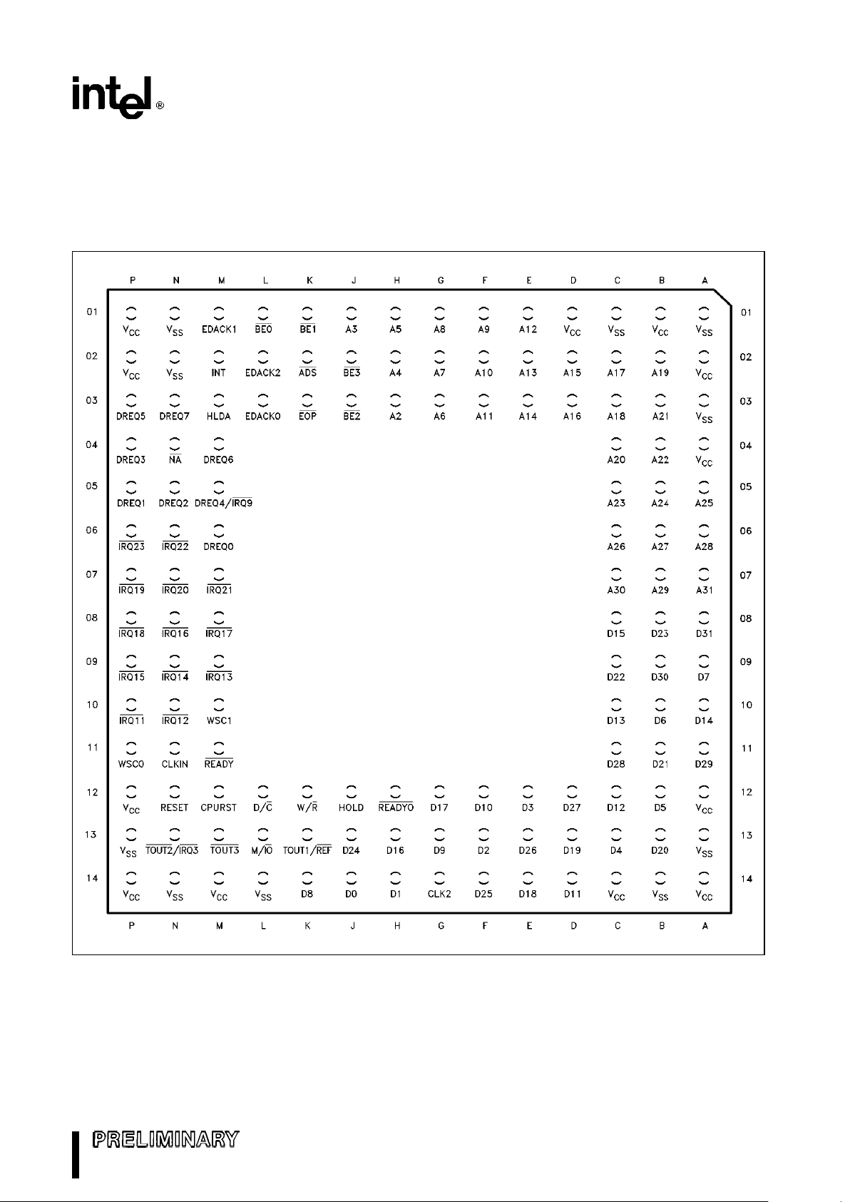
M82380
11.0 INTEL RESERVED I/O PORTS
There are eleven I/O ports in the M82380 address
space which are reserved for Intel future peripheral
device use only. Their address locations are: 2AH,
3DH, 3EH, 45H, 46H, 76H, 77H, 7DH, 7EH, CCH
and CDH. These addresses should not be used in
the system since the M82380 may respond to read/
write operations to these locations and bus contention may occur if any peripheral is assigned to the
same address location.
271070–97
Figure 62. M82380 PGA PinoutÐView from TOP side
99
Page 100
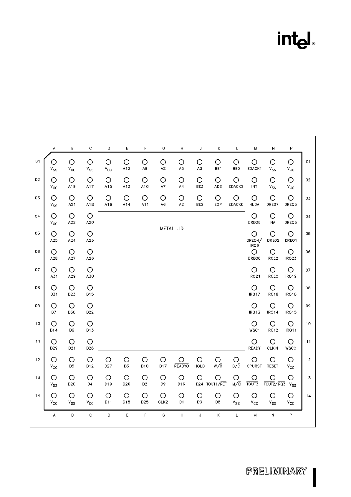
M82380
12.0 MECHANICAL DATA
12.1 Pin Assignment
The M82380 pinout as viewed from the top side of
the PGA component is shown in Figure 62. Its pinout
as viewed from the pin side of the component is
shown in Figure 63. The M82380 pinout as viewed
from the topside of the Quad Flat Pack component
is shown in Figure 64.
V
CC
and GND connections must be made to multi-
ple V
CC
and VSS(GND) pins. Each VCCand V
SS
MUST be connected to the appropriate voltage level. The circuit board should include V
CC
and GND
planes for power distribution and all V
CC
pins must
be connected to the appropriate plane.
Table 17 shows the pin assignments for the PGA
component while Table 18 shows the pin assignments for the Quad Flat Pack.
271070–98
Figure 63. M82380 PGA PinoutÐView from PIN side
100
 Loading...