

TL1453C
DUAL PULSE-WIDTH-MODULATION CONTROL CIRCUIT
SLVS039A – FEBRUARY 1990 – REVISED DECEMBER 1990
1
POST OFFICE BOX 655303 • DALLAS, TEXAS 75265
D
Complete PWM Power Control Circuitry
D
Completely Synchronized Operation
D
Internal Undervoltage Lockout Protection
D
Wide Supply Voltage Range
D
Oscillator Frequency...500 kHz Max
D
Variable Dead Time Provides Control
Over Total Range
D
Internal Regulator Provides a Stable 2.5-V
Reference Supply
description
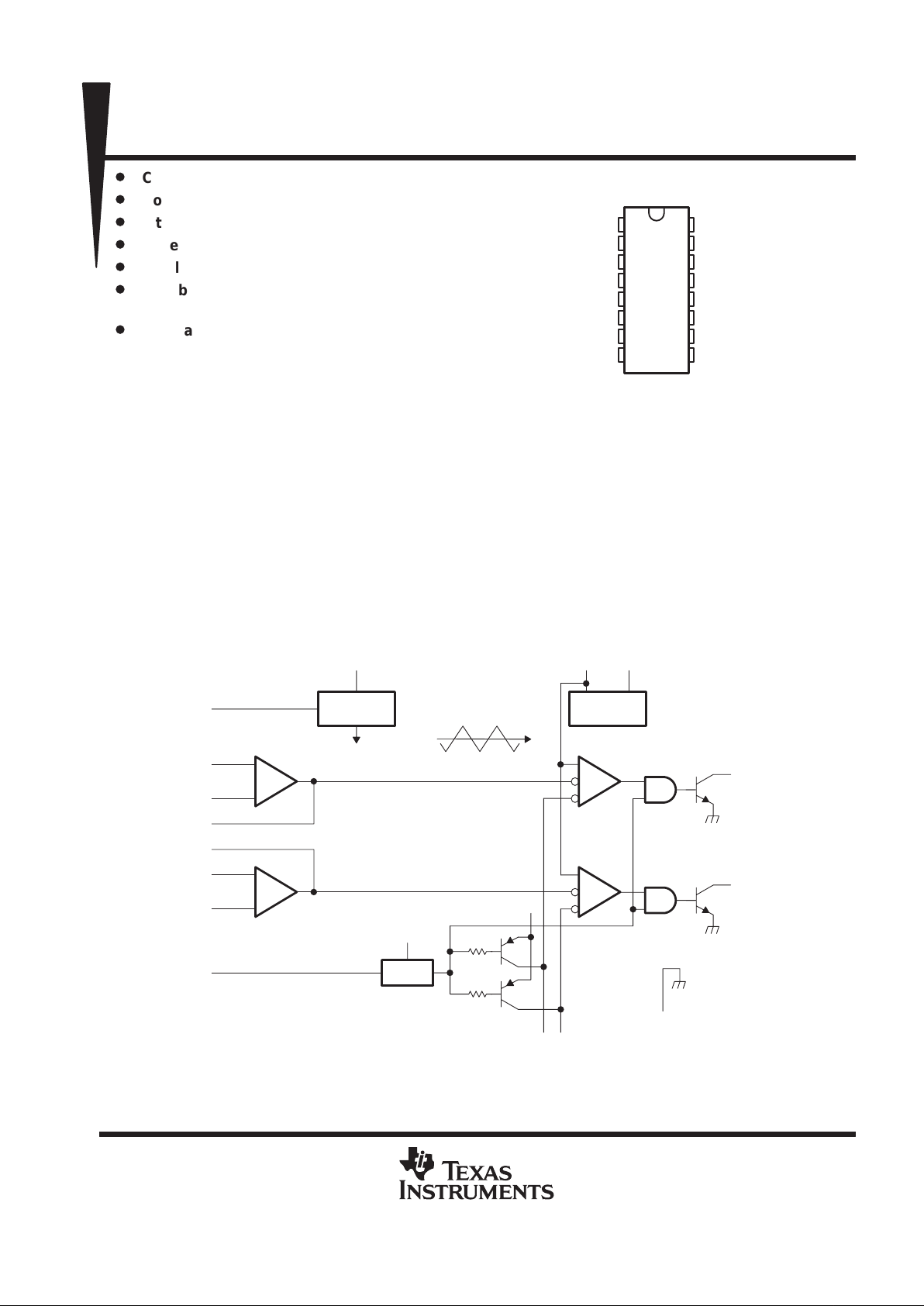
The TL1453C incorporates the functions required in the construction of two pulse-width-modulation control
circuits on a single monolithic chip. Designed primarily for power supply control, the TL1453C contains an
on-chip 2.5-V regulator, two error amplifiers, an adjustable oscillator , two dead-time comparators, undervoltage
lockout circuitry, and dual common-emitter output transistor circuits.
The uncommitted output transistors provide common-emitter output capability for each controller. The internal
amplifiers exhibit a common-mode voltage range from 1.05 V to 1.45 V . The dead-time control comparator has
no offset unless externally altered and may be used to provide 0% to 100% dead time. The on-chip oscillator
may be operated by terminating R
T
(pin 2) and CT (pin 1). During low-VCC conditions, the undervoltage lockout
control circuit feature inhibits the output until the internal circuitry is operational.
The TL1453C is characterized for operation from –20°C to 85°C.
functional block diagram
15
13
14
12
5
4
3
16
SCP
2 IN–
2 IN+
2 FEEDBACK
1 FEEDBACK
1 IN–
1 IN+
REF
GND
8
1 DEAD-TIME CONTROL 2 DEAD-TIME CONTROL
2.5 V
2.5 V
UVLO
†
116
2 OUTPUT
1 OUTPUT
10
7
PWM Comparator 2
PWM Comparator 1
Error Amp.2
1.4 V
2 V
Oscillator
Triangle
Error Amp.1
2.5 V
Voltage
Reference
V
ref
= 2.5 V
V
CC
12
C
T
R
T
2
9
1
†
UVLO = Undervoltage Lockout Protection
Copyright 1990, Texas Instruments Incorporated
PRODUCTION DATA information is current as of publication date.
Products conform to specifications per the terms of Texas Instruments
standard warranty. Production processing does not necessarily include
testing of all parameters.
1
2
3
4
5
6
7
8
16
15
14
13
12
11
10
9
C
T
R
T
ERROR IN+
AMPLIFIER 1 IN–
1 FEEDBACK
1 DEAD-TIME CONTROL
1 OUTPUT
GND
REF
SCP
IN+ ERROR
IN– AMPLIFIER 2
2 FEEDBACK
2 DEAD-TIME CONTRO
L
2 OUTPUT
V
CC
N OR NS PACKAGE
(T0P VIEW)
{
}
TL1453C
DUAL PULSE-WIDTH-MODULATION CONTROL CIRCUIT
SLVS039A – FEBRUARY 1990 – REVISED DECEMBER 1990
2
POST OFFICE BOX 655303 • DALLAS, TEXAS 75265
absolute maximum ratings over operating free-air temperature range (unless otherwise noted)
Supply voltage, V
CC
(see Note 1) 41 V. . . . . . . . . . . . . . . . . . . . . . . . . . . . . . . . . . . . . . . . . . . . . . . . . . . . . . . . . . .
Amplifier input voltage 20 V. . . . . . . . . . . . . . . . . . . . . . . . . . . . . . . . . . . . . . . . . . . . . . . . . . . . . . . . . . . . . . . . . . . . . .
Collector output voltage 51 V. . . . . . . . . . . . . . . . . . . . . . . . . . . . . . . . . . . . . . . . . . . . . . . . . . . . . . . . . . . . . . . . . . . . .
Collector output current 21 mA. . . . . . . . . . . . . . . . . . . . . . . . . . . . . . . . . . . . . . . . . . . . . . . . . . . . . . . . . . . . . . . . . . .
Continuous total power dissipation See Dissipation Rating Table. . . . . . . . . . . . . . . . . . . . . . . . . . . . . . . . . . . . .
Operating free-air temperature range, T
A
–20°C to 85°C. . . . . . . . . . . . . . . . . . . . . . . . . . . . . . . . . . . . . . . . . . . .
Storage temperature range –65°C to 150°C. . . . . . . . . . . . . . . . . . . . . . . . . . . . . . . . . . . . . . . . . . . . . . . . . . . . . . . .
Lead temperature 1,6 mm (1/16 inch) from case for 10 seconds 260°C. . . . . . . . . . . . . . . . . . . . . . . . . . . . . . .
NOTE 1: All voltage values are with respect to network ground terminal.
DISSIPATION RATING TABLE
PACKAGE
TA ≤ 25°C
POWER RATING
DERATING FACTOR
ABOVE TA = 25°C
TA = 85°C
POWER RATING
N 1000 mW 8 mW/°C 520 mW
NS 725 mW 5.8 mW/°C 397 mW
recommended operating conditions
MIN MAX UNIT
Supply voltage, V
CC
3.6 40 V
Amplifier input voltage, V
I
1.05 1.45 V
Collector output voltage, V
O
50 V
Collector output current 20 mA
Current into feedback terminal 45 µA
Feedback resistor, R
F
100 kΩ
Timing capacitor , C
T
150 15000 pF
Timing resistor , R
T
5.1 100 kΩ
Oscillator frequency 1 500 kHz
Operating free-air temperature, T
A
–20 85 °C
electrical characteristics over recommended operating free-air temperature range, VCC = 6 V,
f = 200 kHz (unless otherwise noted)
reference section
PARAMETER TEST CONDITIONS MIN TYP†MAX UNIT
Output voltage (pin 16) IO = 1 mA 2.4 2.5 2.6 V
p
p
TA = –20°C to 25°C –0.1% ±1%
Output voltage change with temperature
TA = 25°C to 85°C –0.2% ±1%
Input regulation VCC = 3.6 V to 40 V 2 12.5 mV
Output regulation IO = 0.1 mA to 1 mA 1 7.5 mV
Short-circuit output current VO = 0 3 10 30 mA
†
All typical values are at TA = 25°C.
TL1453C
DUAL PULSE-WIDTH-MODULATION CONTROL CIRCUIT
SLVS039A – FEBRUARY 1990 – REVISED DECEMBER 1990
3
POST OFFICE BOX 655303 • DALLAS, TEXAS 75265
electrical characteristics over recommended operating free-air temperature range, VCC = 6 V,
f = 200 kHz (unless otherwise noted) (continued)
undervoltage lockout section
PARAMETER TEST CONDITIONS MIN TYP†MAX UNIT
Upper threshold voltage (pin 9) I
Oref
= 0.1 mA, TA = 25°C 2.72 V
Lower threshold voltage (pin 9) I
Oref
= 0.1 mA, TA = 25°C 2.6 V
Hysteresis (pin 9) I
Oref
= 0.1 mA, TA = 25°C 80 120 mV
oscillator section
PARAMETER TEST CONDITIONS MIN TYP†MAX UNIT
Frequency CT = 330 pF, RT = 10 kΩ 200 kHz
Standard deviation of frequency VCC, TA, RT, CT values are constant 10%
Frequency change with voltage VCC = 3.6 V to 40 V 1%
p
TA = –20°C to 25°C –0.4% ±2%
Frequency change with tem erature
TA = 25°C to 85°C –0.2% ±2%
dead-time control section
PARAMETER TEST CONDITIONS MIN TYP†MAX UNIT
Input bias current (pins 6 and 11) 1 µA
Zero duty cycle 2.05 2.25
I
nput threshold voltage at f =
10kHz (pi
ns 6 and
11)
Maximum duty cycle 1.2 1.45
V
error-amplifier section
PARAMETER TEST CONDITIONS MIN TYP†MAX UNIT
Input offset voltage VO (pins 5 and 12) = 1.25 V ±6 mV
Input offset current VO (pins 5 and 12) = 1.25 V ±100 nA
Input bias current VO (pins 5 and 12) = 1.25 V 160 500 nA
1.05
Common-mode input voltage range VCC = 3.6 V to 40 V
1.05
to
V
gg
CC
1.45
Open-loop voltage amplification RF = 200 kΩ 70 80 dB
Unity-gain bandwidth 1.5 MHz
Common-mode rejection ratio 60 80 dB
Positive output voltage swing V
ref
–0.1 V
Negative output voltage swing 1 V
Output (sink) current (pins 5 and 12) VID = –0.1 V, VO = 1.25 V 0.5 1.6 mA
Output (source) current (pins 5 and 12)
VID = 0.1 V, VO = 1.25 V
–45 –70 µA
output section
PARAMETER TEST CONDITIONS MIN TYP†MAX UNIT
VCC = 0, VO = 50 V 10
Collector off-state current
VO = 50 V 10
µ
A
Output saturation voltage IO = 10 mA 1.2 2 V
Short-circuit output current VO = 6 V 90 mA
†
All typical values are at TA = 25°C.

TL1453C
DUAL PULSE-WIDTH-MODULATION CONTROL CIRCUIT
SLVS039A – FEBRUARY 1990 – REVISED DECEMBER 1990
4
POST OFFICE BOX 655303 • DALLAS, TEXAS 75265
electrical characteristics over recommended operating free-air temperature range, VCC = 6 V,
f = 200 kHz (unless otherwise noted) (continued)
pwm comparator section
PARAMETER TEST CONDITIONS MIN TYP†MAX UNIT
p
p
Zero duty cycle 2.05 2.25
Input threshold voltage at f
= 10 kHz
(pins 5 and 12)
Maximum duty cycle 1.2 1.45
V
Input (sink) current (pins 5 and 12) VI = 1.25 V 0.5 1.6 mA
Input (source) current (pins 5 and 12) VI = 1.25 V –45 –70 µA
total device
PARAMETER TEST CONDITIONS MIN TYP†MAX UNIT
Standby supply current Off-state 1.3 1.8 mA
Average supply current RT = 10 kΩ 1.7 2.4 mA
†
All typical values are at TA = 25°C.
test circuit
0.1 µF
OUTPUT 1
OUTPUT 2
9
10
11
12
13
14
15
16
2 OUTPUT
CONTROL
2 DEAD-TIME
2 FEEDBACK
IN–2
IN+2
SCP
REF
GND
1 OUTPUT
CONTROL
1 DEAD-TIME
1 FEEDBACK
IN–1
IN+1
8
7
6
5
4
3
2
1
INPUT
TEST
INPUT
TEST
R
T
C
T
R
T
V
CC
V
CC
R
L
R
L
TL1453C
C
T
330 pF
10 kΩ

TL1453C
DUAL PULSE-WIDTH-MODULATION CONTROL CIRCUIT
SLVS039A – FEBRUARY 1990 – REVISED DECEMBER 1990
5
POST OFFICE BOX 655303 • DALLAS, TEXAS 75265
N (R-PDIP-T**) PLASTIC DUAL-IN-LINE PACKAGE
20
0.975
(24,77)
0.940
(23,88)
18
0.920
0.850
14
0.775
0.745
(19,69)
(18,92)
16
0.775
(19,69)
(18,92)
0.745
A MIN
DIM
A MAX
PINS **
0.310 (7,87)
0.290 (7,37)
(23.37)
(21.59)
Seating Plane
0.010 (0,25) NOM
14/18 PIN ONL Y
4040049/C 08/95
9
8
0.070 (1,78) MAX
A
0.035 (0,89) MAX
0.020 (0,51) MIN
16
1
0.015 (0,38)
0.021 (0,53)
0.200 (5,08) MAX
0.125 (3,18) MIN
0.240 (6,10)
0.260 (6,60)
M
0.010 (0,25)
0.100 (2,54)
0°–15°
16 PIN SHOWN
NOTES: A. All linear dimensions are in inches (millimeters).
B. This drawing is subject to change without notice.
C. Falls within JEDEC MS-001 (20 pin package is shorter then MS-001.)

TL1453C
DUAL PULSE-WIDTH-MODULATION CONTROL CIRCUIT
SLVS039A – FEBRUARY 1990 – REVISED DECEMBER 1990
6
POST OFFICE BOX 655303 • DALLAS, TEXAS 75265
NS (R-PDSO-G**) PLASTIC SMALL-OUTLINE PACKAGE
4040062/B 02/95
14 PIN SHOWN
2,00 MAX
A
0,05 MIN
Seating Plane
1,05
0,55
1
14
PINS **
5,60
5,00
7
8,20
7,40
8
A MIN
A MAX
DIM
Gage Plane
0,15 NOM
0,25
9,90 9,90
10,501410,50
16
12,30 14,70
15,3012,90
20 24
0,10
1,27
0°–10°
M
0,25
0,35
0,51
NOTES: A. All linear dimensions are in millimeters.
B. This drawing is subject to change without notice.
C. Body dimensions do not include mold flash or protrusion, not to exceed 0,15.

IMPORTANT NOTICE
T exas Instruments and its subsidiaries (TI) reserve the right to make changes to their products or to discontinue
any product or service without notice, and advise customers to obtain the latest version of relevant information
to verify, before placing orders, that information being relied on is current and complete. All products are sold
subject to the terms and conditions of sale supplied at the time of order acknowledgement, including those
pertaining to warranty, patent infringement, and limitation of liability.
TI warrants performance of its semiconductor products to the specifications applicable at the time of sale in
accordance with TI’s standard warranty. Testing and other quality control techniques are utilized to the extent
TI deems necessary to support this warranty. Specific testing of all parameters of each device is not necessarily
performed, except those mandated by government requirements.
CERT AIN APPLICATIONS USING SEMICONDUCTOR PRODUCTS MAY INVOLVE POTENTIAL RISKS OF
DEATH, PERSONAL INJURY, OR SEVERE PROPERTY OR ENVIRONMENTAL DAMAGE (“CRITICAL
APPLICATIONS”). TI SEMICONDUCTOR PRODUCTS ARE NOT DESIGNED, AUTHORIZED, OR
WARRANTED TO BE SUITABLE FOR USE IN LIFE-SUPPORT DEVICES OR SYSTEMS OR OTHER
CRITICAL APPLICATIONS. INCLUSION OF TI PRODUCTS IN SUCH APPLICA TIONS IS UNDERST OOD TO
BE FULLY AT THE CUSTOMER’S RISK.
In order to minimize risks associated with the customer’s applications, adequate design and operating
safeguards must be provided by the customer to minimize inherent or procedural hazards.
TI assumes no liability for applications assistance or customer product design. TI does not warrant or represent
that any license, either express or implied, is granted under any patent right, copyright, mask work right, or other
intellectual property right of TI covering or relating to any combination, machine, or process in which such
semiconductor products or services might be or are used. TI’s publication of information regarding any third
party’s products or services does not constitute TI’s approval, warranty or endorsement thereof.
Copyright 1998, Texas Instruments Incorporated
 Loading...