

TL026C
DIFFERENTIAL HIGH-FREQUENCY AMPLIFIER WITH AGC
SLFS007A – JUNE 1985 – REVISED JUL Y 1990
1
POST OFFICE BOX 655303 • DALLAS, TEXAS 75265
D
Low Output Common-Mode Sensitivity to
AGC V oltages
D
Input and Output Impedances Independent
of AGC Voltage
D
Peak Gain . . . 38 dB Typ
D
Wide AGC Range . . . 50 dB Typ
D
3-dB Bandwidth . . . 50 MHz
D
Other Characteristics Similar to NE592 and
uA733
description
This device is a monolithic two-stage highfrequency amplifier with differential inputs and
outputs.
Internal feedback provides wide bandwidth, low phase distortion, and excellent gain stability. Variable gain
based on signal summation provides large AGC control over a wide bandwidth with low harmonic distortion.
Emitter-follower outputs enable the device to drive capacitive loads. All stages are current-source biased to
obtain high common-mode and supply-voltage rejection ratios. The gain may be electronically attenuated by
applying a control voltage to the AGC pin. No external compensation components are required.
This device is particularly useful in TV and radio IF and RF AGC circuits, as well as magnetic-tape and disk-file
systems where AGC is needed. Other applications include video and pulse amplifiers where a large AGC range,
wide bandwidth, low phase shift, and excellent gain stability are required.
The TL026C is characterized for operation from 0°C to 70°C.
absolute maximum ratings over operating free-air temperature range (unless otherwise noted)
†
Supply voltage, V
CC+
(see Note 1) 8 V. . . . . . . . . . . . . . . . . . . . . . . . . . . . . . . . . . . . . . . . . . . . . . . . . . . . . . . . . . . .
Supply voltage, V
CC–
(see Note 1) – 8 V. . . . . . . . . . . . . . . . . . . . . . . . . . . . . . . . . . . . . . . . . . . . . . . . . . . . . . . . . .
Differential input voltage ±5 V. . . . . . . . . . . . . . . . . . . . . . . . . . . . . . . . . . . . . . . . . . . . . . . . . . . . . . . . . . . . . . . . . . . .
Common-mode input voltage ±6 V. . . . . . . . . . . . . . . . . . . . . . . . . . . . . . . . . . . . . . . . . . . . . . . . . . . . . . . . . . . . . . . .
Output current ±10 mA. . . . . . . . . . . . . . . . . . . . . . . . . . . . . . . . . . . . . . . . . . . . . . . . . . . . . . . . . . . . . . . . . . . . . . . . . .
Continuous total dissipation See Dissipation Rating Table. . . . . . . . . . . . . . . . . . . . . . . . . . . . . . . . . . . . . . . . . . .
Operating free-air temperature range 0°C to 70°C. . . . . . . . . . . . . . . . . . . . . . . . . . . . . . . . . . . . . . . . . . . . . . . . . .
Storage temperature range – 65°C to 150°C. . . . . . . . . . . . . . . . . . . . . . . . . . . . . . . . . . . . . . . . . . . . . . . . . . . . . . .
Lead temperature range 1,6 mm (1/16 inch) from case for 10 seconds 260°C. . . . . . . . . . . . . . . . . . . . . . . . . .
†
Stresses beyond those listed under absolute maximum ratings may cause permanent damage to the device. This is a stress rating only, and
functional operation of the device at these or any other conditions beyond those indicated in the recommended operating conditions section of
this specification is not implied. Exposure to absolute-maximum-rated conditions for extended periods may affect device reliability .
NOTE 1: All voltages are with respect to the midpoint of V
CC+
and V
CC–
except differential input and output voltages.
DISSIPATION RATING TABLE
PACKAGE
TA ≤ 25°C
POWER RATING
OPERATING FACTOR
ABOVE TA = 25°C
TA = 70°C
POWER RATING
D 725 mW 5.8 mW/°C 464 mW
P 1000 mW 8.0 mW/°C 640 mW
Copyright 1990, Texas Instruments Incorporated
PRODUCTION DATA information is current as of publication date.
Products conform to specifications per the terms of Texas Instruments
standard warranty. Production processing does not necessarily include
testing of all parameters.
IN–
REF OUT
V
CC
+
OUT–
1
2
3
4
8
7
6
5
IN+
AGC
V
CC
OUT+
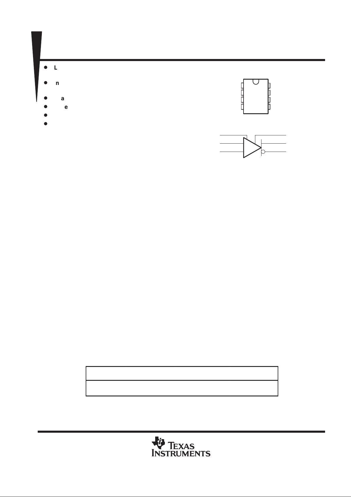
D OR P PACKAGE
(TOP VIEW)
symbol
+
–
AGC
IN +
IN –
7
4
5
2
1
8
REF OUT
OUT+
OUT–
TL026C
DIFFERENTIAL HIGH-FREQUENCY AMPLIFIER WITH AGC
SLFS007A – JUNE 1985 – REVISED JUL Y 1990
2
POST OFFICE BOX 655303 • DALLAS, TEXAS 75265
recommended operating conditions
MIN NOM MAX UNIT
Supply voltage, VCC
+
3 6 8 V
Supply voltage, VCC
–
– 3 – 6 – 8 V
Operating free-air temperature range, T
A
0 70 °C
electrical characteristics at 25°C operating free-air temperature, V
CC+
= ±6 V , V
AGC
= 0, REF OUT pin
open (unless otherwise specified)
PARAMETER FIGURE TEST CONDITIONS MIN TYP MAX UNIT
A
VD
Large-signal differential voltage
amplification
1 V
O(PP)
= 3 V, RL = 2 kΩ 65 85 105 V/V
∆A
VD
Change in voltage amplification 1
V
IPP
= 28.5 mV , RL = 2 kΩ,
V
AGC
– V
ref
= ±180 mV
– 50 dB
V
ref
Voltage at REF OUT I
ref
= – 1 mA to 100 µA 1.3 1.5 V
BW Bandwidth (–3 dB) 2
V
O(PP)
= 1 V,
V
AGC
– V
ref
= ±180 mV
50 MHz
I
IO
Input offset current 0.4 5 µA
I
IB
Input bias current 10 30 µA
V
ICR
Common-mode input voltage range 3 ±1 V
V
OC
Common-mode output voltage 1 RL = ∞ 3.25 3.75 4.25 V
∆V
OC
Change in common-mode output voltage 1 V
AGC
= 0 to 2 V, RL = ∞ 300 mV
V
OO
Output offset voltage 1 VID = 0, RL = ∞ 0.75 V
V
O(PP)
Maximum peak-to-peak output voltage
swing
1 RL = 2 kΩ 3 4 V
r
i
Input resistance at AGC, IN+, or IN – 10 30 kΩ
r
o
Output resistance 20 Ω
VIC = ±1 V, f = 100 kHz 60 86
CMRR
Common-mode rejection ratio
3
VIC = ±1 V, f = 5 mHz 60
dB
k
SVR
Supply voltage rejection ratio
(∆VCC / ∆VIO)
4
∆VCC + = ± 0.5 V ,
∆VCC – = ± 0.5 V
50 70 dB
V
n
Broadband equivalent noise voltage 4 BW = 1 kHz to 10 MHz 12 µV
t
pd
Propagation delay time 2 ∆VO = 1 V 6 10 ns
t
r
Rise time 2 ∆VO = 1 V 4.5 12 ns
I
sink(max)
Maximum output sink current VID = 1 V, VO = 3 V 3 4 mA
I
CC
Supply current No load, No signal 22 27 mA
TL026C
DIFFERENTIAL HIGH-FREQUENCY AMPLIFIER WITH AGC
SLFS007A – JUNE 1985 – REVISED JUL Y 1990
3
POST OFFICE BOX 655303 • DALLAS, TEXAS 75265
electrical characteristics over recommended operating free-air temperature range, V
CC
±
= ±6 V,
V
AGC
= 0, REF OUT pin open (unless otherwise specified)
PARAMETER FIGURE TEST CONDITIONS MIN TYP MAX UNIT
A
VD
Large-signal differential voltage amplification 1 V
O(PP)
= 3 V, RL = 2 kΩ 55 115 V/V
I
IO
Input offset current 6 µA
I
IB
Input bias current 40 µA
V
ICR
Common-mode input voltage range 3 ±1 V
V
OO
Output offset voltage 1 VID = 0, RL = ∞ 1.5 V
V
O(PP)
Maximum peak-to-peak output voltage swing 1 RL = 2 kΩ 2.8 V
r
i
Input resistance at AGC, IN+, or IN – 8 kΩ
CMRR Common-mode rejection ratio 3 VIC = ±1 V, f = 100 kHz 50 dB
k
SVR
Supply voltage rejection ratio
(∆VCC / ∆VIO)
4
∆VCC + = ± 0.5 V ,
∆VCC – = ± 0.5 V
50 dB
I
sink(max)
Maximum output sink current VID = 1 V, VO = 3 V 2.8 4 mA
I
CC
Supply current 1 No load, No signal 30 mA
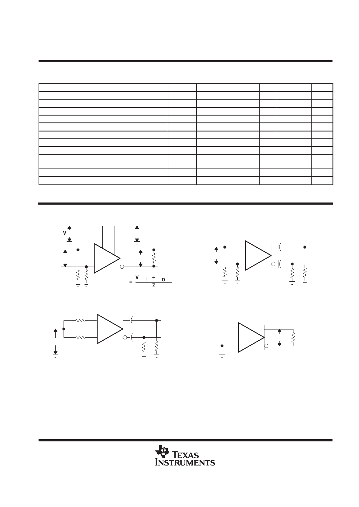
PARAMETER MEASUREMENT INFORMATION
IN +
IN –
AGC
OUT +
OUT –
REF OUT
R
L
50 Ω 50 Ω
VOC+
V
O
)
)
V
O
*
2
+
–
V
AGC
V
ref
V
ID
V
OD
Figure 1. Test Circuit
1 kΩ1 kΩ
VO
+
VO
–
50 Ω 50 Ω
+
–
V
ID
0.2 µF
0.2 µF
Figure 2. Test Circuit
1 kΩ1 kΩ
VO
+
VO
–
50 Ω
50 Ω
+
–
0.2 µF
0.2 µF
V
IC
Figure 3. Test Circuit
RL = 2 kΩ
+
–
V
OD
Figure 4. Test Circuit

TL026C
DIFFERENTIAL HIGH-FREQUENCY AMPLIFIER WITH AGC
SLFS007A – JUNE 1985 – REVISED JUL Y 1990
4
POST OFFICE BOX 655303 • DALLAS, TEXAS 75265
TYPICAL CHARACTERISTICS
Figure 5
– 200 – 100 0 100 200
A
DIFFERENTIAL VOLTAGE AMPLIFICATION
vs
DIFFERENTIAL GAIN-CONTROL VOLTAGE
VD
V
AGC
– V
ref
– Differential Gain-Control Voltage – mV
100
90
80
70
60
50
40
30
20
10
0
VCC + = 6 V
VCC – = – 6 V
TA = 0°C
TA = 70°C
TA = 25°C
— Differential Voltage Amplification — V/ V

TL026C
DIFFERENTIAL HIGH-FREQUENCY AMPLIFIER WITH AGC
SLFS007A – JUNE 1985 – REVISED JUL Y 1990
5
POST OFFICE BOX 655303 • DALLAS, TEXAS 75265
APPLICATION INFORMATION
gain characteristics
Figure 5 shows the differential voltage amplification versus the differential gain-control voltage (V
AGC
– V
ref
).
V
AGC
is the absolute voltage applied to the AGC input and V
ref
is the dc voltage at the REF OUT output. As V
AGC
increases with respect to V
ref
, the TL026C gain changes from maximum to minimum. As shown in Figure 5 for
example, V
AGC
would have to vary from approximately 180 mV less than V
ref
to approximately 180 mV greater
than V
ref
to change the gain from maximum to minimum. The total signal change in V
AGC
is defined by the
following equation.
∆V
AGC
= V
ref
+ 180 mV – (V
ref
– 180 mV)
∆V
AGC
= 360 mV
(1)
However, because V
AGC
varies as the ac AGC signal varies and also differentially around V
ref
, then V
AGC
should
have an ac signal component and a dc component. To preserve the dc and thermal tracking of the device, this
dc voltage must be generated from V
ref
. To apply proper bias to the AGC input, the external circuit used to
generate V
AGC
must combine these two voltages. Figures 6 and 7 show two circuits that will perform this
operation and are easy to implement. The circuits use a standard dual operational amplifier for AGC feedback.
By providing rectification and the required feedback gain, these circuits are also complete AGC systems.
circuit operation
Amplifier A1 amplifies and inverts the rectified and filtered AGC signal voltage VC producing output voltage V1.
Amplifier A2 is a differential amplifier that inverts V1 again and adds the scaled V
ref
voltage. This conditioning
makes V
AGC
the sum of the signal plus the scaled V
ref
. As the signal voltage increases, V
AGC
increases and
the gain of the TL026C is reduced. This maintains a constant output level.
feedback circuit equations
Following the AGC input signal (Figures 6 and 7) from the OUT output through the feedback amplifiers to the
AGC input produces the following equations:
(2)
1. AC ouput to diode D1, assuming sinusoidal signals
V
O
= VOP (sin (wt))
where:
V
OP
= peak voltage of V
O
(3)
2. Diode D1 and capacitor C1 output
VC = VOP – V
F
where:
VF = forward voltage drop of D1
V
C
= voltage across capacitor C1
(4)
3. A1 output
V1
+*
R2
R1
V
C
(5)
4. A2 output (R3 = R4)
V
AGC
+
R2
R1
VC)
2
R6
R5)R6
V
ref

TL026C
DIFFERENTIAL HIGH-FREQUENCY AMPLIFIER WITH AGC
SLFS007A – JUNE 1985 – REVISED JUL Y 1990
6
POST OFFICE BOX 655303 • DALLAS, TEXAS 75265
APPLICATION INFORMATION
Amplifier A2 inverts V1 producing a positive AGC signal voltage. Therefore, the input voltage to the TL026C
AGC pin consists of an AGC signal equal to:
(6)
R2
R1
V
C
and a dc voltage derived from V
ref
, defined as the quiescent value of V
AGC
.
V
AGC
(q)+2
R6
R5)R6
V
ref
(7)
For the initial resistor calculations, V
ref
is assumed to be typically 1.4 V making quiescent V
AGC
approximately
1.22 V (V
AGC
(q) = V
ref
– 180 mV). This voltage allows the TL026C to operate at maximum gain under no-signal
and low-signal conditions. In addition, with V
ref
used as both internal and external reference, its variation from
device to device automatically adjusts the overall bias and makes AGC operation essentially independent of
the absolute value of V
ref
. The resistor divider needs to be calculated only once and is valid for the full tolerance
of V
ref
.
output voltage limits (see Figures 6 and 7)
The output voltage level desired must fall within the following limits:
1. Because the data sheet minimum output swing is 3 V peak-to-peak using a 2-kΩ load resistor , the
user-selected design limit for the peak output swing should not exceed 1.5 V.
2. The voltage drop of the rectifying diode determines the lower voltage limit. When a silicon diode is
used, this voltage is approximately 0.7 V. The output voltage V
O
must have sufficient amplitude to
exceed the rectifying diode drop. Aschottky diode can be used to reduce the V
O
level required.
gain calculations for a peak output voltage of 1 V
A peak output voltage of 1 V was chosen for gain calculations because it is approximately midway between the
limits of conditions 1 and 2 in the preceding paragraph.
Using equation 3 (VC = VOP – Vd), VC is calculated as follows:
V
C
= 1 V – 0.7 V
VC = 0.3 V
Therefore, the gain of A1 must produce a voltage V1 that is equal to or greater than the total change in V
AGC
for maximum TL026C gain change.
With a total change in V
AGC
of 360 mV and using equation 4, the calculation is as follows:
*
V1
V
C
+
D
V
AGC
V
C
+
R2
R1
+
0.36
0.3
+
1.2
If R1 is 10 kΩ, R2 is 1.2 time R1 or 12 kΩ.
Since the output voltage for this circuit must be between 0.85 V and 1.3 V, the component values in
Figures 6 and 7 provide a nominal 1-V peak output limit. This limit is the best choice to allow for temperature
variations of the diode and minimum output voltage specification.

TL026C
DIFFERENTIAL HIGH-FREQUENCY AMPLIFIER WITH AGC
SLFS007A – JUNE 1985 – REVISED JUL Y 1990
7
POST OFFICE BOX 655303 • DALLAS, TEXAS 75265
APPLICATION INFORMATION
The circuit values in Figures 6 and 7 will produce the best results in this general application. Because of
rectification and device input constraints, the circuit in Figure 6 will not provide attenuation and has about
32 dB of control range. The circuit shown in Figure 7 will have approximately 25% variation in the peak output
voltage limit due to the variation in gain of the TL592 device to device. In addition, if a lower output voltage is
desired, the output of the TL026C can be used for approximately 40 mV of controlled signal.
considerations for the use of the TL026C
To obtain the most reliable results, RF breadboarding techniques must be used. A groundplane board should
be used and power supplies should be bypassed with 0.1-µF capacitors. Input leads and output leads should
be as short as possible and separated from each other.
A peak input voltage greater than 200 mV will begin to saturate the input stages of the TL026C and, while the
circuit is in the AGC mode, the output signal may become distorted.
To observe the output signal of TL026C or TL592, low-capacitance FET probes or the output voltage divider
technique shown in Figure 6 should be used.
–
+
+
–
OUT +
OUT –
0.1 µF
0.1 µF
REF
OUT
30 kΩ
To Scope
Monitor
V
out
200 Ω
1.8 kΩ
IN –
IN +
50 Ω
AGC
10 kΩ
10 kΩ
V
AGC
A2
20 kΩ
50 Ω
V
I
+
–
10 kΩ
A1
12 kΩ
1N914
D1
0.1 µF
V1
1/2 TL082
1/2 TL082
TL026C
NOTE: V
CC+
= 6 V and V
CC–
= – 6 V for TL026C and amplifiers A1 and A2.
Figure 6. Typical Application Circuit With No Attenuation

TL026C
DIFFERENTIAL HIGH-FREQUENCY AMPLIFIER WITH AGC
SLFS007A – JUNE 1985 – REVISED JUL Y 1990
8
POST OFFICE BOX 655303 • DALLAS, TEXAS 75265
APPLICATION INFORMATION
–
+
R6
20 kΩ
50 Ω
0.1 µF
V
OUT –
V
OUT +
0.1 µF
A1
50 Ω
10 kΩ
R1
12 kΩ
R2
1/2 TL082
0.1 µF
OUT –
OUT +
IN –
IN +
AGC
To Scope
Monitor
–
+
A2
10 kΩ
R4
1/2 TL082
30 kΩ
R5
10 kΩ
R3
V
AGC
V
I
1.8 kΩ
200 Ω
1N914
REF
OUT
TL026C
0.1 µF
TL592
2 kΩ
2 kΩ
510 Ω
+
–
+
–
X20
Gain
NOTE: VCC + = 6 V and VCC – = – 6 V for TL026C and amplifiers A1 and A2.
Figure 7. Typical Application Circuit With Attenuation

IMPORTANT NOTICE
T exas Instruments and its subsidiaries (TI) reserve the right to make changes to their products or to discontinue
any product or service without notice, and advise customers to obtain the latest version of relevant information
to verify, before placing orders, that information being relied on is current and complete. All products are sold
subject to the terms and conditions of sale supplied at the time of order acknowledgement, including those
pertaining to warranty, patent infringement, and limitation of liability.
TI warrants performance of its semiconductor products to the specifications applicable at the time of sale in
accordance with TI’s standard warranty. Testing and other quality control techniques are utilized to the extent
TI deems necessary to support this warranty. Specific testing of all parameters of each device is not necessarily
performed, except those mandated by government requirements.
CERT AIN APPLICATIONS USING SEMICONDUCT OR PRODUCTS MAY INVOLVE POTENTIAL RISKS OF
DEATH, PERSONAL INJURY, OR SEVERE PROPERTY OR ENVIRONMENTAL DAMAGE (“CRITICAL
APPLICATIONS”). TI SEMICONDUCTOR PRODUCTS ARE NOT DESIGNED, AUTHORIZED, OR
WARRANTED TO BE SUITABLE FOR USE IN LIFE-SUPPORT DEVICES OR SYSTEMS OR OTHER
CRITICAL APPLICATIONS. INCLUSION OF TI PRODUCTS IN SUCH APPLICA TIONS IS UNDERSTOOD T O
BE FULLY AT THE CUSTOMER’S RISK.
In order to minimize risks associated with the customer’s applications, adequate design and operating
safeguards must be provided by the customer to minimize inherent or procedural hazards.
TI assumes no liability for applications assistance or customer product design. TI does not warrant or represent
that any license, either express or implied, is granted under any patent right, copyright, mask work right, or other
intellectual property right of TI covering or relating to any combination, machine, or process in which such
semiconductor products or services might be or are used. TI’s publication of information regarding any third
party’s products or services does not constitute TI’s approval, warranty or endorsement thereof.
Copyright 1998, Texas Instruments Incorporated
 Loading...