Texas Instruments THS4012IDR, THS4011IDR, THS4011MFKB, THS4011IDGNR, THS4011IDGN Datasheet
...
THS4011, THS4012
290-MHz LOW-DISTORTION HIGH-SPEED AMPLIFIERS
SLOS216B – JUNE 1999 – FEBRUARY 2000
1
POST OFFICE BOX 655303 • DALLAS, TEXAS 75265
D
Very High Speed
– 290 MHz Bandwidth (G = 1, –3 dB)
– 310 V/µs Slew Rate
– 37 ns Settling Time (0.1%)
D
Very Low Distortion
– THD = –80 dBc (f = 1 MHz, R
L
= 150 Ω)
D
110 mA Output Current Drive (Typical)
D
7.5 nV/√Hz Voltage Noise
D
Excellent Video Performance
– 70 MHz Bandwidth (0.1 dB, G = 1)
– 0.006% Differential Gain Error
– 0.01° Differential Phase Error
D
±5 V to ±15 V Supply Voltage
D
Available in Standard SOIC, MSOP
PowerPAD, JG, or FK Packages
D
Evaluation Module Available
description
The THS401 1 and THS4012 are very high speed,
single/dual, voltage feedback amplifiers ideal for
a wide range of applications. The devices offer
very good ac performance with 290-MHz
bandwidth, 310-V/µs slew rate, and 37-ns settling
time (0.1%). These amplifiers have a high output
drive capability of 110 mA and draw only 7.8-mA
supply current per channel. For applications
requiring low distortion, the THS4011/12 operate
with a total harmonic distortion (THD) of –80 dBc
at f = 1 MHz. For video applications, the
THS401 1/12 offer 0.1 dB gain flatness to 70-MHz,
0.006% differential gain error, and 0.01°
differential phase error.
RELATED DEVICES
DEVICE DESCRIPTION
THS4011/2
THS4031/2
THS4061/2
290-MHz Low Distortion High-Speed Amplifiers
100-MHz Low Noise High Speed-Amplifiers
180-MHz High-Speed Amplifiers
CAUTION: THE THS4011 AND THS4012 provide ESD protection circuitry . However , permanent damage can still occur if this device
is subjected to high-energy electrostatic discharges. Proper ESD precautions are recommended to avoid any performance
degradation or loss of functionality.
Copyright 2000, Texas Instruments Incorporated
Please be aware that an important notice concerning availability, standard warranty, and use in critical applications of
Texas Instruments semiconductor products and disclaimers thereto appears at the end of this data sheet.
PRODUCTION DATA information is current as of publication date.
Products conform to specifications per the terms of Texas Instruments
standard warranty. Production processing does not necessarily include
testing of all parameters.
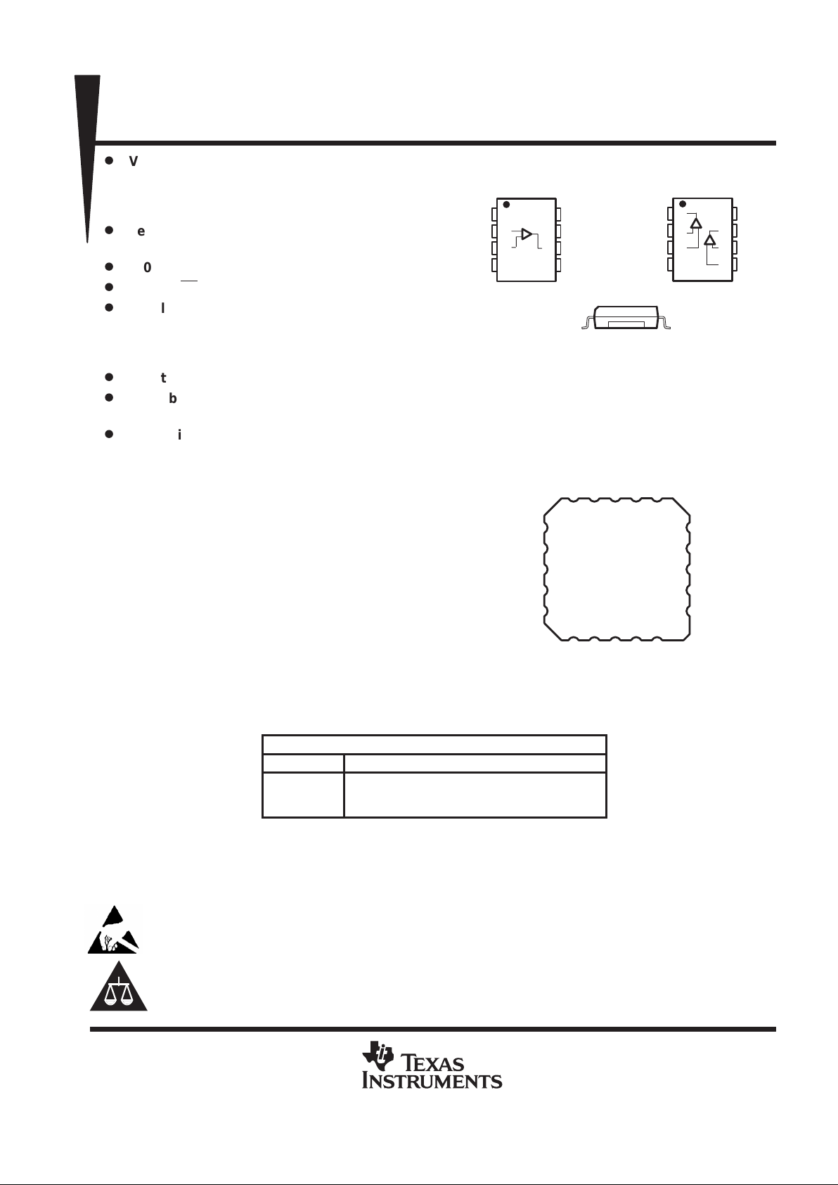
NC
IN–
NC
IN+
NC
THS4012
D AND DGN† PACKAGE
(TOP VIEW)
1
2
3
4
8
7
6
5
1OUT
1IN–
1IN+
–V
CC
V
CC+
2OUT
2IN–
2IN+
1
2
3
4
8
7
6
5
NULL
IN–
IN+
V
CC–
NULL
V
CC+
OUT
NC
THS4011
JG, D AND DGN PACKAGE
(TOP VIEW)
NC – No internal connection
Cross Section View Showing
PowerPAD Option (DGN)
†
This device is in the Product Preview stage of development.
Please contact your local TI sales office for availability.
1920132
17
18
16
15
14
1312119 10
5
4
6
7
8
NC
V
CC+
NC
OUT
NC
NC
NULLNCNULL
NC
V
NCNCNC
NC
THS4011
FK PACKAGE
(TOP VIEW)
CC–
On products compliant to MIL-PRF-38535, all parameters are tested
unless otherwise noted. On all other products, production
processing does not necessarily include testing of all parameters.
THS4011, THS4012
290-MHz LOW-DISTORTION HIGH-SPEED AMPLIFIERS
SLOS216B – JUNE 1999 – FEBRUARY 2000
2
POST OFFICE BOX 655303 • DALLAS, TEXAS 75265
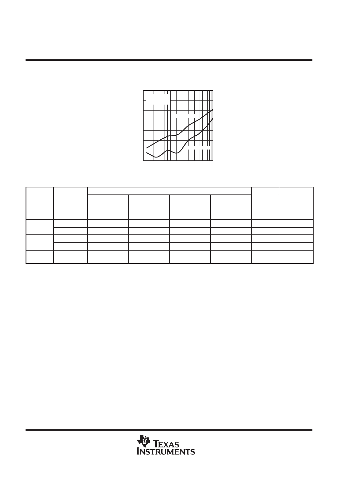
DISTORTION
vs
FREQUENCY
–40
–50
–60
–70
–80
–90
100k 1M 10M
f – Frequency – Hz
–100
Distortion – dB
–110
2nd Harmonic
VCC = ± 15 V
RL = 150 Ω
G = 2
3rd Harmonic
AVAILABLE OPTIONS
PACKAGED DEVICES
T
A
NUMBER OF
CHANNELS
PLASTIC
SMALL
OUTLINE
†
(D)
PLASTIC
MSOP
†
(DGN)
CERAMIC
DIP
(JG)
CHIP
CARRIER
(FK)
MSOP
SYMBOL
EVALUATION
MODULE
0°C to
1 THS4011CD THS4011CDGN — — TIACM THS4011EVM
70°C
2 THS4012CD THS4012CDGN
‡
— — TIABD THS4012EVM
–40°C to
1 THS4011ID THS4011IDGN — — TIACN —
85°C
2 THS4012ID THS4012IDGN
‡
— — TIABZ —
–55°C to
125°C
1 — — THS4011MJG THS4011MFK — —
†
The D and DGN packages are available taped and reeled. Add an R suffix to the device type (i.e., THS401 1CDGNR).
‡
This device is in the Product Preview stage of development. Please contact your local TI sales office for availability.
THS4011, THS4012
290-MHz LOW-DISTORTION HIGH-SPEED AMPLIFIERS
SLOS216B – JUNE 1999 – FEBRUARY 2000
3
POST OFFICE BOX 655303 • DALLAS, TEXAS 75265
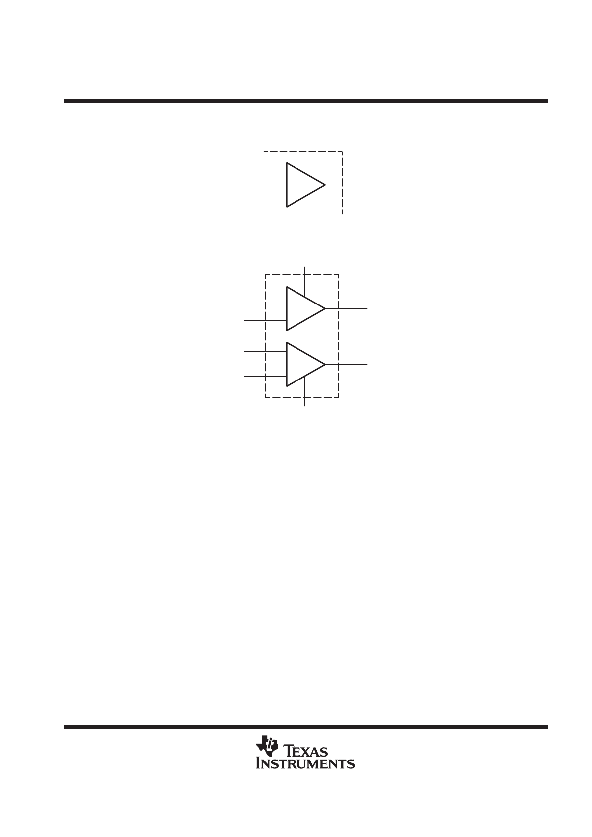
functional block diagram
OUT
8
6
1
IN–
IN+
2
3
Null
–
+
Figure 1. THS4011 – Single Channel
1OUT
1IN–
1IN+
V
CC
2OUT
2IN–
2IN+
–V
CC
8
6
1
2
3
5
7
4
–
+
–
+
Figure 2. THS4012 – Dual Channel
THS4011, THS4012
290-MHz LOW-DISTORTION HIGH-SPEED AMPLIFIERS
SLOS216B – JUNE 1999 – FEBRUARY 2000
4
POST OFFICE BOX 655303 • DALLAS, TEXAS 75265
absolute maximum ratings over operating free-air temperature range (unless otherwise noted)
†
Supply voltage, VCC ±16.5 V. . . . . . . . . . . . . . . . . . . . . . . . . . . . . . . . . . . . . . . . . . . . . . . . . . . . . . . . . . . . . . . . . . . .
Input voltage, VI ±V
CC
. . . . . . . . . . . . . . . . . . . . . . . . . . . . . . . . . . . . . . . . . . . . . . . . . . . . . . . . . . . . . . . . . . . . . . . . . .
Output current, IO 175 mA. . . . . . . . . . . . . . . . . . . . . . . . . . . . . . . . . . . . . . . . . . . . . . . . . . . . . . . . . . . . . . . . . . . . . . .
Differential input voltage, VID ±4 V. . . . . . . . . . . . . . . . . . . . . . . . . . . . . . . . . . . . . . . . . . . . . . . . . . . . . . . . . . . . . . .
Continuous total power dissipation See Dissipation Rating Table. . . . . . . . . . . . . . . . . . . . . . . . . . . . . . . . . . . . .
Maximum junction temperature, T
J
150°C. . . . . . . . . . . . . . . . . . . . . . . . . . . . . . . . . . . . . . . . . . . . . . . . . . . . . . .
Operating free-air temperature, TA, THS401xC 0°C to 70°C. . . . . . . . . . . . . . . . . . . . . . . . . . . . . . . . . . . . . . . .
THS401xI –40°C to 85°C. . . . . . . . . . . . . . . . . . . . . . . . . . . . . . . . . . . . . . .
THS4011M –55°C to 125°C. . . . . . . . . . . . . . . . . . . . . . . . . . . . . . . . . . . . .
Storage temperature, T
stg
–65°C to 150°C. . . . . . . . . . . . . . . . . . . . . . . . . . . . . . . . . . . . . . . . . . . . . . . . . . . . . . . .
Lead temperature, 1,6 mm (1/16 inch) from case for 10 seconds, D, DGN package 300°C. . . . . . . . . . . . . . .
Lead temperature, 1,6 mm (1/16 inch) from case for 60 seconds, JG package 300°C. . . . . . . . . . . . . . . . . . .
Case temperature for 60 seconds, FK package 260°C. . . . . . . . . . . . . . . . . . . . . . . . . . . . . . . . . . . . . . . . . . . . . .
†
Stresses beyond those listed under “absolute maximum ratings” may cause permanent damage to the device. These are stress ratings only, and
functional operation of the device at these or any other conditions beyond those indicated under “recommended operating conditions” is not
implied. Exposure to absolute-maximum-rated conditions for extended periods may affect device reliability.
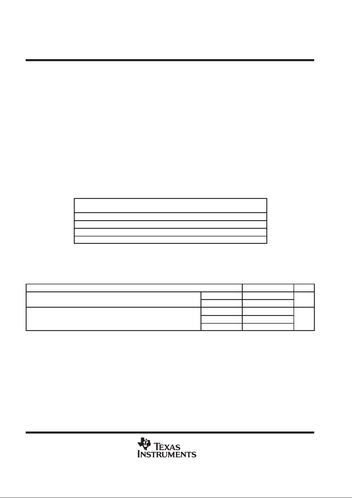
DISSIPATION RATING TABLE
θ
θ
T
= 25°C
PACKAGE
JA
(°C/W)
JC
(°C/W)
A
POWER RATING
D 167
†
38.3 740 mW
DGN
‡
58.4 4.7 2.14 W
JG 119 28 1050 mW
FK 87.7 20 1375 mW
†
This data was taken using the JEDEC standard Low-K test PCB. For the JEDEC Proposed
High-K test PCB, the θJA is 95°C/W with a power rating at TA = 25°C of 1.32 W.
‡
This data was taken using 2 oz. trace and copper pad that is soldered directly to a 3 in. × 3 in.
PC. For further information, refer to
Application Information
section of this data sheet.
recommended operating conditions
MIN NOM MAX UNIT
pp
Split supply ±4.5 ±16
Suppl
y v
oltage, V
CC
Single supply 9 32
V
C suffix 0 70
Operating free-air temperature, T
A
I suffix –40 85
°C
M suffix –55 125
THS4011, THS4012
290-MHz LOW-DISTORTION HIGH-SPEED AMPLIFIERS
SLOS216B – JUNE 1999 – FEBRUARY 2000
5
POST OFFICE BOX 655303 • DALLAS, TEXAS 75265
electrical characteristics, VCC = ±15 V, RL = 150 Ω, TA = 25°C, (unless otherwise noted)
dynamic performance
PARAMETER
TEST CONDITIONS
†
THS4011C/I,
THS4012C/I
UNIT
MIN TYP MAX
VCC = ±15 V 290
Unity-gain bandwidth (–3 dB)
Gain
=
1
VCC = ±5 V 270
MH
z
VCC = ±15 V 70
BW
Bandwidth for 0.1 dB flatness
Gain
=
1
VCC = ±5 V 35
MH
z
p
VCC = ±15 V, RL = 150 Ω V
O(PP)
= 20 V, 4.9
Full power bandwidth (see Note 2)
VCC = ±5 V, RL = 150 Ω, V
O(PP)
= 5 V, 16
MH
z
VCC = ±15 V 310
SR
Slew rate
Gain
= –1,
R
L
=
150 Ω
VCC = ±5 V 260
V/µs
VCC = ±15 V 37
Settling time to 0.1%
V
I
= –2.5 V to 2.5 V,
Gain
= –
1
VCC = ±5 V 35
ns
t
s
VCC = ±15 V 90
Settling time to 0.01%
V
I
= –2.5 V to 2.5 V,
Gain
= –
1
VCC = ±5 V 70
ns
†
Full range = 0°C to 70°C for the C suffix and –40°C to 85°C for the I suffix.
noise/distortion performance
PARAMETER
TEST CONDITIONS
†
THS4011C/I,
THS4012C/I
UNIT
MIN TYP MAX
THD Total harmonic distortion
VCC = ±15 V ,
V
O(PP)
= 2 V
fc = 1 MHz,
–80 dBc
V
n
Input voltage noise VCC = ±5 V or ±15 V, f = 10 kHz 7.5 nV/√Hz
I
n
Input current noise VCC = ±5 V or ±15 V, f = 10 kHz 1 pA/√Hz
Gain = 2,
VCC = ±15 V 0.01%
Differential gain error
R
L
=
150 Ω
,
NTSC
VCC = ±5 V 0.01%
p
Gain = 2,
VCC = ±15 V 0.01°
Differential phase error
R
L
=
150 Ω
,
NTSC
VCC = ±5 V 0.001°
†
Full range = 0°C to 70°C for the C suffix and –40°C to 85°C for the I suffix.
THS4011, THS4012
290-MHz LOW-DISTORTION HIGH-SPEED AMPLIFIERS
SLOS216B – JUNE 1999 – FEBRUARY 2000
6
POST OFFICE BOX 655303 • DALLAS, TEXAS 75265
electrical characteristics at TA = 25°C, VCC = ±15 V , RL = 150 Ω (unless otherwise noted) (continued)
dc performance
PARAMETER
TEST CONDITIONS
†
THS4011C/I,
THS4012C/I
UNIT
MIN TYP MAX
VCC = ±15 V ,
TA = 25°C 10 25
p
p
V
O
=
±10 V
,
RL = 1 kΩ
TA = full range 8
V/mV
Open loop gain
VCC = ±5 V,
TA = 25°C 7 12
V
O
= ±2.5 V,
RL = 250 Ω
TA = full range 5
V/mV
p
TA = 25°C 1 6
VIOInput offset voltage
V
CC
= ±5 V or
±15 V
TA = full range 8
mV
Input offset voltage drift 15 µV/°C
p
TA = 25°C 2 6
IIBInput bias current
V
CC
=
±5 V or ±15 V
TA = full range 8
µ
A
p
TA = 25°C 25 250
IIOInput offset current
V
CC
= ±5 V or
±15 V
TA = full range 400
nA
Offset current drift VCC = ±5 V or ±15 V 0.3 nA/°C
†
Full range = 0°C to 70°C for the C suffix and –40°C to 85°C for the I suffix.
input characteristics
PARAMETER
TEST CONDITIONS
†
THS4011C/I,
THS4012C/I
UNIT
MIN TYP MAX
p
VCC = ±15 V ±13 ±14.1
V
ICR
Common-mode input voltage range
VCC = ±5 V ±3.8 ±4.3
V
V
= ±15 V ,
TA = 25°C 82 110 dB
CC
,
VIC = ±12 V
TA = full range 77 dB
CMRR
Common-mode rejection ratio
V
= ±5 V,
TA = 25°C 90 95
CC
,
VIC = ±2.5 V
TA = full range 83
dB
R
I
Input resistance 2 MΩ
C
I
Input capacitance 1.2 pF
†
Full range = 0°C to 70°C for the C suffix and –40°C to 85°C for the I suffix.
output characteristics
PARAMETER
TEST CONDITIONS
†
THS4011C/I,
THS4012C/I
UNIT
MIN TYP MAX
VCC = ±15 V
±13 ±13.5
p
VCC = ±5 V
R
L
= 1
kΩ
±3.4 ±3.7
VOOutput voltage swing
VCC = ±15 V RL = 250 Ω ±12 ±13
V
VCC = ±5 V RL = 150 Ω ±3 ±3.4
p
VCC = ±15 V 70 110
IOOutput current
R
L
= 20 Ω,
VCC = ±5 V 50 75
mA
I
OS
Short-circuit output current VCC = ±15 V 150 mA
R
O
Output resistance Open loop 12 Ω
†
Full range = 0°C to 70°C for the C suffix and –40°C to 85°C for the I suffix.
THS4011, THS4012
290-MHz LOW-DISTORTION HIGH-SPEED AMPLIFIERS
SLOS216B – JUNE 1999 – FEBRUARY 2000
7
POST OFFICE BOX 655303 • DALLAS, TEXAS 75265
electrical characteristics at TA = 25°C, VCC = ±15 V , RL = 150 Ω (unless otherwise noted) (continued)
power supply
PARAMETER
TEST CONDITIONS
†
THS4011C/I,
THS4012C/I
UNIT
MIN TYP MAX
pp
Dual supply ±4.5 ±16.5
VCCSuppl
y v
oltage
Single supply 9 33
V
TA = 25°C 7.8 9.5
pp
p
V
CC
=
±15 V
TA = full range 11
ICCSupply current (each amplifier)
TA = 25°C 6.9 8.5
mA
V
CC
= ±5
V
TA = full range 10
pp
TA = 25°C 75 83
PSRR
Power supply rejection ratio
V
CC
= ±5 V to
±15 V
TA = full range 68
dB
†
Full range = 0°C to 70°C for the C suffix and –40°C to 85°C for the I suffix.
THS4011, THS4012
290-MHz LOW-DISTORTION HIGH-SPEED AMPLIFIERS
SLOS216B – JUNE 1999 – FEBRUARY 2000
8
POST OFFICE BOX 655303 • DALLAS, TEXAS 75265
electrical characteristics, VCC = ±15 V, RL = 150 Ω, TA = 25°C, (unless otherwise noted)
dynamic performance
THS4011M
PARAMETER
TEST CONDITIONS
†
MIN TYP MAX
UNIT
Unity-gain bandwidth Closed loop, RL = 1 kΩ VCC = ±15 V *160 200 MHz
VCC = ±15 V 70
Bandwidth for 0.1 dB flatness Gain = 1
VCC = ±5 V 35
MHz
BW
VCC = ±2.5 V 30
p
VCC = ±15 V, RL = 150 Ω, V
O(PP)
= 20 V 2.5
Full power bandwidth (see Note 1)
VCC = ±5 V, RL = 150 Ω, V
O(PP)
= 20 V 8
MH
z
SR Slew rate VCC = ±15 V, RL = 1 kΩ *300 400 V/µs
VCC = ±15 V 37
Settling time to 0.1%
V
I
= –2.5 V to 2.5 V,
Gain
= –
1
VCC = ±5 V 35
ns
t
s
VCC = ±15 V 90
Settling time to 0.01%
V
I
= –2.5 V to 2.5 V,
Gain
= –
1
VCC = ±5 V 70
ns
†
Full range = –55°C to 125°C for the M suffix.
*This parameter is not tested.
NOTE 1: Full pwer bandwidth = slew rate/2π V
(PP)
.
noise/distortion performance
THS4011M
PARAMETER
TEST CONDITIONS
†
MIN TYP MAX
UNIT
THD Total harmonic distortion
VCC = ±15 V , fc = 1 MHz,
V
O(PP)
= 1 V
–80 dBc
V
n
Input voltage noise VCC = ±5 V or ±15 V, f = 10 kHz 7.5 nV/√Hz
I
n
Input current noise VCC = ±5 V or ±15 V, f = 10 kHz 1 pA/√Hz
Gain = 2,
VCC = ±15 V 0.006
Differential gain error
R
L
=
150 Ω
,
NTSC
VCC = ±5 V 0.001
%
p
Gain = 2,
VCC = ±15 V 0.01°
Differential phase error
R
L
=
150 Ω
,
NTSC
VCC = ±5 V 0.002°
†
Full range = –55°C to 125°C for the M suffix.
THS4011, THS4012
290-MHz LOW-DISTORTION HIGH-SPEED AMPLIFIERS
SLOS216B – JUNE 1999 – FEBRUARY 2000
9
POST OFFICE BOX 655303 • DALLAS, TEXAS 75265
electrical characteristics at TA = full range, VCC = ±15 V, RL = 1 kΩ (unless otherwise noted)
(continued)
dc performance
THS4011M
PARAMETER
TEST CONDITIONS
†
MIN TYP MAX
UNIT
p
p
VCC = ±15 V , VO = ±10 V ,
RL = 1 kΩ
TA = full range 6 14 V/mV
Open loop gain
VCC = ±5 V, VO = ±2.5 V ,
RL = 1 kΩ
TA = full range 5 10 V/mV
p
TA = 25°C 2 6
VIOInput offset voltage
V
CC
= ±5 V or
±15 V
TA = full range 2 8
mV
Input offset voltage drift VCC = ±5 V or ±15 V 15 µV/°C
p
TA = 25°C 2 6
IIBInput bias current
V
CC
= ±5 V or
±15 V
TA = full range 4 8
µ
A
I
IO
Input offset current VCC = ±5 V or ±15 V 25 250 nA
Offset current drift VCC = ±5 V or ±15 V TA = 25°C 0.3 nA/°C
†
Full range = –55°C to 125°C for the M suffix.
input characteristics
THS4011M
PARAMETER
TEST CONDITIONS
†
MIN TYP MAX
UNIT
p
VCC = ±15 V ±13 ±14.1
V
ICR
Common-mode input voltage range
VCC = ±5 V ±3.8 ±4.3
V
VCC = ±15 V , VIC = ±12 V 75 90
CMRR
Common-mode rejection ratio
VCC = ±5 V, VIC = ±2.5 V 84 95
dB
R
I
Input resistance 2 MΩ
C
I
Input capacitance 1.2 pF
†
Full range = –55°C to 125°C for the M suffix.
output characteristics
THS4011M
PARAMETER
TEST CONDITIONS
†
MIN TYP MAX
UNIT
VCC = ±15 V
±13 ±13.5
p
VCC = ±5 V
R
L
= 1
kΩ
±3.4 ±3.7
VOOutput voltage swing
VCC = ±15 V RL = 250 Ω ±12 ±13
V
VCC = ±5 V RL = 150 Ω ±3 ±3.4
p
VCC = ±15 V
70 115
IOOutput current
VCC = ±5 V
R
L
=
20 Ω
50 75
mA
I
OS
Short-circuit output current VCC = ±15 V TA = 25°C 150 mA
R
O
Output resistance Open loop 12 Ω
†
Full range = –55°C to 125°C for the M suffix.
 Loading...