

www.ti.com
0
0.01
0.02
0.03
0.04
0.05
0.06
0.07
0 1 2 3 4 5 6 7 8
Number of 150 Ω Loads
Differential Gain − %
PAL
NTSC
Gain = 2,
RF = 649 Ω,
VS = ±15 V,
40 IRE − NTSC and PAL,
Worst Case ±100 IRE Ramp
+
−
75 Ω
75 Ω
75 Ω
75 Ω
75 Ω
n Lines
V
O(1)
V
O(n)
75-Ω Transmission Line
V
I
649 Ω 649 Ω
−15 V
15 V
0
0.02
0.04
0.06
0.08
0.1
0.12
0.14
0 1 2 3 4 5 6 7 8
Number of 150 Ω Loads
Differential Phase − deg
PAL
NTSC
Gain = 2,
RF = 649 Ω,
VS = ±15 V,
40 IRE − NTSC and PAL,
Worst Case ±100 IRE Ramp
DIFFERENTIAL PHASE
vs
NUMBER OF LOADS
DIFFERENTIAL GAIN
vs
NUMBER OF LOADS
VIDEO DISTRIBUTION AMPLIFIER APPLICATION
查询THS3120供应商
LOW-NOISE, HIGH-OUTPUT DRIVE, CURRENT-FEEDBACK,
FEATURES DESCRIPTION
• Low Noise
– 1 pA/ √ Hz Noninverting Current Noise
– 10 pA/ √ Hz Inverting Current Noise
– 2.5 nV/ √ Hz Voltage Noise
• High Output Current Drive: 475 mA
• High Slew Rate: 1700 V/ µs (R
V
= 8 V
O
)
PP
• Wide Bandwidth: 120 MHz (G = 2, R
• Wide Supply Range: ± 5 V to ± 15 V
• Power-Down Feature: (THS3120 Only)
APPLICATIONS
• Video Distribution
• Power FET Driver
• Pin Driver
• Capacitive Load Driver
= 50 Ω,
L
THS3120, THS3121
SLOS420A – SEPTEMBER 2003 – REVISED NOVEMBER 2003
OPERATIONAL AMPLIFIERS
The THS3120 and THS3121 are low-noise,
high-voltage, high output current drive, currentfeedback amplifiers designed to operate over a wide
supply range of ± 5 V to ± 15 V for today's high
performance applications.
The THS3120 offers a power saving mode by providing a power-down pin for reducing the 7-mA quiescent current of the device, when the device is not
= 50 Ω)
L
active.
These amplifiers provide well-regulated ac
performance characteristics. Most notably, the 0.1-dB
flat bandwidth is exceedingly high, reaching beyond
90 MHz. The unity gain bandwidth of 130 MHz allows
for good distortion characteristics at 10 MHz. Coupled
with high 1700-V/ µs slew rate, the THS3120 and
THS3121 amplifiers allow for high output voltage
swings at high frequencies.
The THS3120 and THS3121 are offered in a 8-pin
SOIC (D), and the 8-pin MSOP (DGN) packages with
PowerPAD™.
PowerPAD is a trademark of Texas Instruments.
PRODUCTION DATA information is current as of publication date.
Products conform to specifications per the terms of the Texas
Instruments standard warranty. Production processing does not
necessarily include testing of all parameters.
Please be aware that an important notice concerning availability, standard warranty, and use in critical applications of Texas
Instruments semiconductor products and disclaimers thereto appears at the end of this data sheet.
Copyright © 2003, Texas Instruments Incorporated
www.ti.com
1
2
3
4
8
7
6
5
NC
V
IN−
V
IN+
V
S−
NC
V
S+
V
OUT
NC
D, DGNTOP VIEWD, DGNTOP VIEW
NC = No Internal Connection
1
2
3
4
8
7
6
5
REF
V
IN−
V
IN+
V
S−
PD
V
S+
V
OUT
NC
NC = No Internal Connection
THS3120 THS3121
Note: The device with the power down option defaults to the ON state if no signal is applied to the PD pin. Additionallly, the REF pin
functional range is from VS− to (VS+ − 4 V).
THS3120, THS3121
SLOS420A – SEPTEMBER 2003 – REVISED NOVEMBER 2003
This integrated circuit can be damaged by ESD. Texas Instruments recommends that all integrated circuits be handled with
appropriate precautions. Failure to observe proper handling procedures and installation procedures can cause damage.
AVAILABLE OPTIONS
T
A
0 ° C to 70 ° C AQA
-40 ° C to 85 ° C APN
0 ° C to 70 ° C AQO
-40 ° C to 85 ° C APO
(1) Available in tape and reel. The R suffix standard quantity is 2500 (e.g. THS3120CDGNR).
(2) The PowerPAD is electrically isolated from all other pins.
PLASTIC SMALL OUTLINE SOIC (D) PLASTIC MSOP (DGN)
THS3120CD THS3120CDGN
THS3120CDR THS3120CDGNR
THS3120ID THS3120IDGN
THS3120IDR THS3120IDGNR
THS3121CD THS3121CDGN
THS3121CDR THS3121CDGNR
THS3121ID THS3121IDGN
THS3121IDR THS3121IDGNR
PACKAGED DEVICE
(1) (2)
SYMBOL
DISSIPATION RATING TABLE
POWER RATING
TJ= 125 ° C
PACKAGE Θ
(1)
D-8
(2)
DGN-8
(1) This data was taken using the JEDEC standard low-K test PCB. For the JEDEC proposed high-K test PCB, the Θ
power rating at TA= 25 ° C of 1.05 W.
(2) This data was taken using 2 oz. trace and copper pad that is soldered directly to a 3 inch x 3 inch PCB. For further information, refer to
the Application Information section of this data sheet.
( ° C/W) Θ
JC
38.3 95 1.05 W 421 mW
4.7 58.4 1.71 W 685 W
( ° C/W)
JA
TA= 25 ° C TA= 85 ° C
2
JA
is 95 ° C/W with
www.ti.com
THS3120, THS3121
SLOS420A – SEPTEMBER 2003 – REVISED NOVEMBER 2003
RECOMMENDED OPERATING CONDITIONS
MIN NOM MAX UNIT
Supply voltage V
Operating free-air temperature, T
A
Operating junction temperature, continuous operating, T
Normal storage temperature, T
stg
ABSOLUTE MAXIMUM RATINGS
over operating free-air temperature (unless otherwise noted)
Supply voltage, VS-to V
Input voltage, V
Differential input voltage, V
Output current, I
Continuous power dissipation See Dissipation Ratings Table
Maximum junction temperature, T
Maximum junction temperature, continuous operation, long term reliability, T
Operating free-air temperature, T
Storage temperature, T
Lead temperature 1,6 mm (1/16 inch) from case for 10 seconds 300 ° C
ESD ratings:
(1) Stresses beyond those listed under absolute maximum ratings may cause permanent damage to the device. These are stress ratings
only, and functional operation of the device at these or any other conditions beyond those indicated under, , recommended operating
conditions” is not implied. Exposure to absolute-maximum-rated conditions for extended periods may affect device reliability.
(2) The THS3120 and THS3121 may incorporate a PowerPAD™ on the underside of the chip. This acts as a heatsink and must be
connected to a thermally dissipating plane for proper power dissipation. Failure to do so may result in exceeding the maximum junction
temperature which could permanently damage the device. See TI Technical Brief SLMA002 for more information about utilizing the
PowerPAD™ thermally enhanced package.
(3) The absolute maximum temperature under any condition is limited by the constraints of the silicon process.
(4) The maximum junction temperature for continuous operation is limited by the package constraints. Operation above this temperature
may result in reduced reliability and/or lifetime of the device.
S+
I
(2)
O
ID
(3)
J
A
stg
HBM 1000
CDM 1500
MM 200
Dual supply ± 5 ± 15
Single supply 10 30
Commercial 0 70
Industrial -40 85
J
-40 125 ° C
-40 85 ° C
(1)
550 mA
150 ° C
(4)
J
125 ° C
Commercial 0 ° C to 70 ° C
Industrial -40 ° C to 85 ° C
-65 ° C to 125 ° C
UNIT
± 4 V
33 V
± V
S
° C
3

www.ti.com
THS3120, THS3121
SLOS420A – SEPTEMBER 2003 – REVISED NOVEMBER 2003
ELECTRICAL CHARACTERISTICS
VS= ±15 V, RF= 649 Ω,R
PARAMETER TEST CONDITIONS
AC PERFORMANCE
Small-signal bandwidth, -3 dB
0.1 dB bandwidth flatness G = 2, RF= 649 Ω , VO= 200 mV
Large-signal bandwidth G = 5, RF= 499 Ω , VO= 2 V
Slew rate (25% to 75% level) V/µs TYP
Slew rate 900 V/µs MAX
Rise and fall time G = -5, VO= 10-V step, RF= 499 Ω 10 ns TYP
Settling time to 0.1% G = -2, VO= 2 VPPstep 11
Settling time to 0.01% G = -2, VO= 2 VPPstep 52
Harmonic distortion
2nd Harmonic distortion
3rd Harmonic distortion
Input voltage noise f > 20 kHz 2.5 nV / √ Hz TYP
Noninverting input current noise f > 20 kHz 1 pA / √ Hz TYP
Inverting input current noise f > 20 kHz 10 pA / √ Hz TYP
Differential gain
Differential phase
DC PERFORMANCE
Transimpedance VO= ± 3.75 V, Gain = 1 1.9 1.3 1 1 M Ω MIN
Input offset voltage 2 6 8 8 mV MAX
Average offset voltage drift ± 10 ± 10 µV/ ° C TYP
Noninverting input bias current 1 4 6 6 µA MAX
Average bias current drift ± 10 ± 10 nA/ ° C TYP
Inverting input bias current 3 15 20 20 µA MAX
Average bias current drift ± 10 ± 10 nA/ ° C TYP
Input offset current 4 15 20 20 µA MAX
Average offset current drift ± 30 ± 30 nA/ ° C TYP
INPUT CHARACTERISTICS
Input common-mode voltage range ± 13.3 ± 13 ± 12.8 ± 12.8 V MIN
Common-mode rejection ratio VCM= ± 12.5 V 70 63 60 60 dB MIN
Noninverting input resistance 41 M Ω TYP
Noninverting input capacitance 0.4 pF TYP
OUTPUT CHARACTERISTICS
Output voltage swing V MIN
Output current (sourcing) RL= 25 Ω 475 425 400 400 mA MIN
Output current (sinking) RL= 25 Ω 490 425 400 400 mA MIN
Output impedance f = 1 MHz, Closed loop 0.04 Ω TYP
= 50 Ω, and G = 2 (unless otherwise noted)
L
TYP OVER TEMPERATURE
25 ° C 25 ° C UNIT
G = 1, RF= 806 Ω , VO= 200 mV
G = 2, RF= 649 Ω , VO= 200 mV
G = 5, RF= 499 Ω , VO= 200 mV
G = 10, RF= 301 Ω , VO= 200 mV
G = 1, VO= 4-V step, RF= 806 Ω 1500
G = 2, VO= 8-V step, RF= 649 Ω 1700
Recommended maximum SR for
repetitive signals
G = 2,
RF= 649 Ω ,
VO= 2 VPP,
f = 10 MHz
G = 2,
RL= 150 Ω , TYP
RF= 649 Ω
VCM= 0 V
VCM= 0 V
VCM= 0 V
VCM= 0 V
RL= 1 k Ω ± 14 ± 13.5 ± 13 ± 13
RL= 50 Ω ± 13.5 ± 12.5 ± 12 ± 12
(1)
PP
PP
PP
PP
PP
PP
RL= 50 Ω 51
RL= 499 Ω 53
RL= 50 Ω 50
RL= 499 Ω 65
NTSC 0.007%
PAL 0.007%
NTSC 0.018 °
PAL 0.022 °
130
120
105
66
90
80
0 ° C to -40 ° C to MIN/TYP/
70 ° C 85 ° C MAX
MHz TYP
ns TYP
dBc TYP
(1) For more information, see the Application Information section of this data sheet.
4
www.ti.com
THS3120, THS3121
SLOS420A – SEPTEMBER 2003 – REVISED NOVEMBER 2003
ELECTRICAL CHARACTERISTICS (continued)
VS= ±15 V, RF= 649 Ω,R
PARAMETER TEST CONDITIONS
POWER SUPPLY
Specified operating voltage ± 15 ± 16 ± 16 ± 16 V MAX
Maximum quiescent current 7 8.5 11 11 mA MAX
Minimum quiescent current 7 5.5 4 4 mA MIN
Power supply rejection (+PSRR) VS+= 15.5 V to 14.5 V, VS-= 15 V 83 75 70 70 dB MIN
Power supply rejection (-PSRR) VS+= 15 V, VS-= -15.5 V to -14.5 V 78 70 65 65 dB MIN
POWER-DOWN CHARACTERISTICS
Power-down voltage level V MAX
Power-down quiescent current PD = 0V 300 450 500 500 µA MAX
VPDquiescent current µA TYP
Turnon time delay 90% of final value 4
Turnoff time delay 10% of final value 6
Input impedance 3.4 || 1.7 k Ω || pF TYP
= 50 Ω, and G = 2 (unless otherwise noted)
L
Enable, REF = 0 V ≤ 0.8
Power-down , REF = 0 V ≥ 2
VPD= 0 V, REF = 0 V, 11
VPD= 3.3 V, REF = 0 V 11
TYP OVER TEMPERATURE
25 ° C 25 ° C UNIT
0 ° C to -40 ° C to MIN/TYP/
70 ° C 85 ° C MAX
µs TYP
5
www.ti.com
THS3120, THS3121
SLOS420A – SEPTEMBER 2003 – REVISED NOVEMBER 2003
ELECTRICAL CHARACTERISTICS
VS= ±5 V, RF= 750 Ω, RL= 50 Ω, and G = 2 (unless otherwise noted)
TYP OVER TEMPERATURE
PARAMETER TEST CONDITIONS
AC PERFORMANCE
G = 1, RF= 909 Ω , VO= 200 mV
Small-signal bandwidth, -3 dB
0.1 dB bandwidth flatness G = 2, RF= 750 Ω , VO= 200 mV
Large-signal bandwidth G = 2, RF= 750 Ω , VO= 2 V
Slew rate (25% to 75% level) V/µs TYP
Slew rate 900 V/µs MAX
Rise and fall time G = -5, VO= 5-V step, RF= 499 Ω 10 ns TYP
Settling time to 0.1% G = -2, VO= 2 VPPstep 7
Settling time to 0.01% G = -2, VO= 2 VPPstep 42
Harmonic distortion
2nd Harmonic distortion
3rd Harmonic distortion
Input voltage noise f > 20 kHz 2.5 nV / √ Hz TYP
Noninverting input current noise f > 20 kHz 1 pA / √ Hz TYP
Inverting input current noise f > 20 kHz 10 pA / √ Hz TYP
Differential gain
Differential phase
DC PERFORMANCE
Transimpedance VO= ± 1.25 V, Gain = 1 1.2 0.9 0.7 0.7 M Ω MIN
Input offset voltage 3 6 8 8 mV MAX
Average offset voltage drift ± 10 ± 10 µV/ ° C TYP
Noninverting input bias current 1 4 6 6 µA MAX
Average bias current drift ± 10 ± 10 nA/ ° C TYP
Inverting input bias current 2 15 20 20 µA MAX
Average bias current drift ± 10 ± 10 nA/ ° C TYP
Input offset current 2 15 20 20 µA MAX
Average offset current drift ± 30 ± 30 nA/ ° C TYP
INPUT CHARACTERISTICS
Input common-mode voltage range ± 3.2 ± 2.9 ± 2.8 ± 2.8 V MIN
Common-mode rejection ratio VCM= ± 2.5 V 66 62 58 58 dB MIN
Noninverting input resistance 35 M Ω TYP
Noninverting input capacitance 0.5 pF TYP
OUTPUT CHARACTERISTICS
Output voltage swing V MIN
Output current (sourcing) RL= 10 Ω 310 250 200 200 mA MIN
Output current (sinking) RL= 10 Ω 325 250 200 200 mA MIN
Output impedance f = 1 MHz 0.05 Ω TYP
G = 2, RF= 750 Ω , VO= 200 mV
G = 5, RF= 499 Ω , VO= 200 mV
G = 10, RF= 301 Ω , VO= 200 mV
G = 1, VO= 2-V step, RF= 909 Ω 560
G = 2, VO= 2-V step, RF= 750 Ω 620
Recommended maximum SR for
repetitive signals
G = 2,
RF= 649 Ω ,
VO= 2 VPP,
f = 10 MHz
G = 2,
RL= 150 Ω , TYP
RF= 806 Ω
VCM= 0 V
VCM= 0 V
VCM= 0 V
VCM= 0 V
RL= 1 k Ω ± 4 ± 3.8 ± 3.7 ± 3.7
RL= 50 Ω ± 3.9 ± 3.7 ± 3.6 ± 3.6
(1)
PP
PP
PP
PP
PP
PP
RL= 50 Ω 51
RL= 499 Ω 53
RL= 50 Ω 48
RL= 499 Ω 60
NTSC 0.008%
PAL 0.008%
NTSC 0.014 °
PAL 0.018 °
25 ° C 25 ° C UNIT
105
100
95
70
70
85
0 ° C to -40 ° C to MIN/TYP/
70 ° C 85 ° C MAX
MHz TYP
ns TYP
dBc TYP
(1) For more information, see the Application Information section of this data sheet.
6

www.ti.com
THS3120, THS3121
SLOS420A – SEPTEMBER 2003 – REVISED NOVEMBER 2003
ELECTRICAL CHARACTERISTICS (continued)
VS= ±5 V, RF= 750 Ω, RL= 50 Ω, and G = 2 (unless otherwise noted)
TYP OVER TEMPERATURE
PARAMETER TEST CONDITIONS
POWER SUPPLY
Specified operating voltage ± 5 ± 4.5 ± 4.5 ± 4.5 V MIN
Maximum quiescent current 6.5 8 10 10 mA MAX
Minimum quiescent current 6.5 4 3.5 3.5 mA MIN
Power supply rejection (+PSRR) 80 72 67 67 dB MIN
Power supply rejection (-PSRR) 75 67 62 62 dB MIN
POWER-DOWN CHARACTERISTICS
Power-down voltage level V MAX
Power-down quiescent current PD = 0 V 200 450 500 500 µA MAX
VPDquiescent current µA TYP
Turnon time delay 90% of final value 4
Turnoff time delay 10% of final value 6
Input impedance 3.4 || 1.7 k Ω || pF TYP
VS+= 5.5 V to 4.5 V,
VS-= 5 V
VS+= 5 V,
VS-= -5.5 V to -4.5 V
Enable, REF = 0 V ≤ 0.8
Power-down , REF = 0 V ≥ 0.2
VPD= 0 V, REF = 0 V, 11
VPD= 3.3 V, REF = 0 V 11
25 ° C 25 ° C UNIT
0 ° C to -40 ° C to MIN/TYP/
70 ° C 85 ° C MAX
µs TYP
7
www.ti.com
THS3120, THS3121
SLOS420A – SEPTEMBER 2003 – REVISED NOVEMBER 2003
TYPICAL CHARACTERISTICS
TABLE OF GRAPHS
± 15-V graphs
Noninverting small signal gain frequency response 1, 2
Inverting small signal gain frequency response 3
0.1 dB flatness 4
Noninverting large signal gain frequency response 5
Inverting large signal gain frequency response 6
Frequency response capacitive load 7
Recommended R
2nd Harmonic distortion vs Frequency 9
3rd Harmonic distortion vs Frequency 10
Harmonic distortion vs Output voltage swing 11, 12
Slew rate vs Output voltage step 13, 14
Noise vs Frequency 15
Settling time 16, 17
Quiescent current vs Supply voltage 18
Output voltage vs Load resistance 19
Input bias and offset current vs Case temperature 20
Input offset voltage vs Case temperature 21
Transimpedance vs Frequency 22
Rejection ratio vs Frequency 23
Noninverting small signal transient response 24
Inverting large signal transient response 25
Overdrive recovery time 26
Differential gain vs Number of loads 27
Differential phase vs Number of loads 28
Closed loop output impedance vs Frequency 29
Power-down quiescent current vs Supply voltage 30
Turnon and turnoff time delay 31
± 5-V graphs
Noninverting small signal gain frequency response 32
Inverting small signal gain frequency response 33
0.1 dB flatness 34
Slew rate vs Output voltage step 35, 36
2nd Harmonic distortion vs Frequency 37
3rd Harmonic distortion vs Frequency 38
Harmonic distortion vs Output voltage swing 39, 40
Noninverting small signal transient response 41
Inverting small signal transient response 42
Input bias and offset current vs Case temperature 43
Overdrive recovery time 44
Settling time 45
Rejection ratio vs Frequency 46
ISO
vs Capacitive load 8
FIGURE
8
www.ti.com
0
1
2
3
4
5
6
7
8
9
1 M 10 M 100 M 1 G
f − Frequency − Hz
Noninverting Gain − dB
RF = 475 Ω
RF = 649 Ω
RF = 750 Ω
Gain = 2,
RL = 50 Ω,
VO = 0.2 VPP,
VS = ±15 V
−4
−2
0
2
4
6
8
10
12
14
16
18
20
22
24
100 k 1 M 10 M 100 M 1 G
f − Frequency − Hz
Noninverting Gain − dB
G = 1, RF = 806 Ω
G = 10, RF = 301 Ω
G = 5, RF = 499 Ω
G = 2, RF = 649 Ω
RL = 50 Ω,
VO = 0.2 VPP,
VS = ±15 V
-4
-2
0
2
4
6
8
10
12
14
16
18
20
22
24
100 k 1 M 10 M 100 M 1 G
f - Frequency - Hz
Inverting Gain - dB
G = -1, RF = 681 Ω
G = -10, RF = 365 Ω
G = -5, RF = 499 Ω
G = -2, RF = 681 Ω
RL = 50 Ω,
VO = 0.2 VPP,
VS = ±15 V
0
2
4
6
8
10
12
14
16
100 k 1 M 10 M 100 M 1 G
f − Frequency − Hz
Noninverting Gain − dB
G = 5, RF = 499 Ω
G = 2, RF = 681 Ω
RL = 50 Ω,
VO = 2 VPP,
VS = ±15 V
5.7
5.8
5.9
6
6.1
6.2
6.3
100 k 1 M 10 M 100 M
Gain = 2,
RF = 562 Ω,
RL = 50 Ω,
VO = 0.2 VPP,
VS = ±15 V
f - Frequency - Hz
Noninverting Gain - dB
-4
-2
0
2
4
6
8
10
12
14
16
1 M 10 M 100 M 1 G
f - Frequency - Hz
G = -5, RF = 499 Ω
G =-1, RF = 681 Ω
RL = 50 Ω,
VO = 2 VPP,
VS = ±15 V
Inverting Gain - dB
-2
0
2
4
6
8
10
12
14
16
10 M 100 M
Capacitive Load - Hz
Signal Gain - dB
Gain = 5,
RL = 50 Ω
VS = ±15 V
R
(ISO)
= 49.9 Ω CL = 10 pF
R
(ISO)
= 40.2 Ω
CL = 22 pF
R
(ISO)
= 30 Ω
CL = 47 pF
R
(ISO)
= 20 Ω
CL = 100 pF
0
10
20
30
40
50
60
10 100
C
L
− Capacitive Load − pF
Recommended R Ω
Gain = 5,
RL = 50 Ω,
VS = ±15 V
ISO
Resistance −
-90
-80
-70
-60
-50
-40
-30
1 M 10 M 100 M
f - Frequency - Hz
2 nd Harmonic Distortion - dBc
G = 2,
RF = 649 Ω
G = 2, RF = 649 Ω,
RL = 499 Ω
VO = 2 VPP,
RL = 50 Ω,
VS = ±15 V
G = 5,
RF = 499 Ω
-100
100 k
THS3120, THS3121
SLOS420A – SEPTEMBER 2003 – REVISED NOVEMBER 2003
TYPICAL CHARACTERISTICS ( ±15 V)
NONINVERTING SMALL SIGNAL NONINVERTING SMALL SIGNAL INVERTING SMALL SIGNAL
FREQUENCY RESPONSE FREQUENCY RESPONSE FREQUENCY RESPONSE
Figure 1. Figure 2. Figure 3.
0.1 dB FLATNESS FREQUENCY RESPONSE FREQUENCY RESPONSE
NONINVERTING LARGE SIGNAL INVERTING LARGE SIGNAL
Figure 4. Figure 5. Figure 6.
FREQUENCY RESPONSE vs vs
RECOMMENDED R
ISO
2nd HARMONIC DISTORTION
CAPACITIVE LOAD CAPACITIVE LOAD FREQUENCY
Figure 7. Figure 8. Figure 9.
9

www.ti.com
-90
-80
-70
-60
-50
-40
-30
1 M
10 M 100 M
f - Frequency - Hz
3rd Harmonic Distortion - dBc
G = 2,
RF = 649 Ω,
RL = 499 Ω
VO = 2 VPP,
RL = 50 Ω,
VS = ±15 V
100 k
-100
G = 2,
RF = 649 Ω
G = 5,
RF = 499 Ω
-90
-80
-70
-60
-50
-40
0 1 2 3 4 5 6 7 8 9 10
Harmonic Distortion - dBc
VO - Output Voltage Swing - V
PP
Gain = 2,
RF = 649 Ω,
f = 8 MHz
VS = ±15 V
HD2, RL = 50 Ω
HD3, RL = 499Ω
HD2, RL = 499Ω
HD3, RL = 50 Ω
-100
-95
-90
-85
-80
-75
-70
0 1 2 3 4 5 6 7 8 9 10
Harmonic Distortion - dBc
VO - Output Voltage Swing - V
PP
Gain = 2,
RF = 649 Ω,
f= 1 MHz
VS = ±15 V
HD2, RL = 499Ω
HD3, RL = 50Ω
HD3, RL = 499Ω
HD2, RL = 50Ω
0
200
400
600
800
1000
1200
1400
1600
1800
2000
0 0.5 1 1.5 2 2.5 3 3.5 4 4.5 5
SR − Slew Rate − V/
V
O
− Output Voltage −V
PP
sµ
Gain = 1
RL = 50 Ω
RF = 806 Ω
VS = ±15 V
Fall
Rise
0
200
400
600
800
1000
1200
1400
1600
1800
2000
0 1 2 3 4 5 6 7 8 9 10
SR − Slew Rate − V/
V
O
− Output Voltage −V
PP
sµ
Fall
Rise
Gain = 2
RL = 50 Ω
RF = 649 Ω
VS = ±15 V
1
10
100
0.01 0.1 1 10 100
f - Frequency - kHz
- Current Noise -
V
n
I
n
- Voltage Noise -
pA/ Hz
nV/ Hz
I
n-
I
n+
V
n
−1.25
−1
−0.75
−0.5
−0.25
0
0.25
0.5
0.75
1
1.25
0 2 4 6 8 10 12 14 16
t − Time − ns
− Output Voltage − VV
O
Gain = −2
RL = 50 Ω
RF = 499 Ω
VS = ±15 V
Rising Edge
Falling Edge
−4.5
−4
−3.5
−3
−2.5
−2
−1.5
−1
−0.5
0
0.5
1
1.5
2
2.5
3
3.5
4
4.5
0 2 4 6 8 10 12 14 16
t − Time − ns
− Output Voltage − VV
O
Gain = −2
RL = 50 Ω
RF = 499 Ω
VS = ±15 V
Rising Edge
Falling Edge
0
1
2
3
4
5
6
7
8
9
10
2 3 4 5 6 7 8 9 10 11 12 13 14 15
- Quiescent Current - mAI
Q
VS - Supply Voltage - ±V
TA = 25 °C
TA = -40 °C
TA = 85 °C
THS3120, THS3121
SLOS420A – SEPTEMBER 2003 – REVISED NOVEMBER 2003
TYPICAL CHARACTERISTICS ( ±15 V) (continued)
3rd HARMONIC DISTORTION HARMONIC DISTORTION HARMONIC DISTORTION
vs vs vs
FREQUENCY OUTPUT VOLTAGE SWING OUTPUT VOLTAGE SWING
Figure 10. Figure 11. Figure 12.
SLEW RATE SLEW RATE NOISE
vs vs vs
OUTPUT VOLTAGE STEP OUTPUT VOLTAGE STEP FREQUENCY
10
Figure 13. Figure 14. Figure 15.
SETTLING TIME SETTLING TIME SUPPLY VOLTAGE
Figure 16. Figure 17. #IMPLIED #IMPLIED.
QUIESCENT CURRENT
vs

www.ti.com
−16
−14
−12
−10
−8
−6
−4
−2
0
2
4
6
8
10
12
14
16
10 100 1000
R
L
− Load Resistance − Ω
− Output Voltage − VV
O
VS = ±15 V
TA = −40 to 85°C
0
0.5
1
1.5
2
2.5
3
3.5
4
−40−30−20−10 0 10 20 30 40 50 60 70 80 90
− Input Bias Current −
TC − Case Temperature − °C
VS = ±15 V
− Input Offset Current −
I
IB−
I
IB
Aµ
I
OS
Aµ
I
IB+
I
OS
0
1
2
3
4
5
6
−40−30−20−10 0 10 20 30 40 50 60 70 80 90
VS = ±5 V
VS = ±15 V
T
C
− Case Temperature − °C
− Input Offset Voltage − mV
V
OS
-0.3
-0.25
-0.2
-0.15
-0.1
-0.05
0
0.05
0.1
0.15
0.2
0.25
0.3
0.04 0.05 0.06 0.07 0.08 0.09 0.1 0.11 0.12
t - Time - µs
- Output Voltage - VV
O
Output
Input
Gain = 2,
RL = 50 Ω,
RF = 649 Ω,
VS = ±15 V
0
10
20
30
40
50
60
70
80
90
100
100 k 1 M 10 M 100 M 1 G
f - Frequency - Hz
Transimpedance Gain - dB ohms
VS = ±15 V
VS = ±5 V
0
10
20
30
40
50
60
70
100 k 1 M 10 M 100 M
CMRR
VS = ±15 V
Rejection Ratio − dB
f − Frequency − Hz
PSRR−
PSRR+
-20
-15
-10
-5
0
5
10
15
20
0 0.2 0.4 0.6 0.8 1
-4
-3
-2
-1
0
1
2
3
4
t - Time - µs
Output Voltage - V
- Input Voltage - VV
I
Gain = 2,
RF = 648 Ω,
VS = ±15 V
0
0.01
0.02
0.03
0.04
0.05
0.06
0.07
0 1 2 3 4 5 6 7 8
Number of 150 Ω Loads
Differential Gain − %
PAL
NTSC
Gain = 2,
RF = 649 Ω,
VS = ±15 V,
40 IRE − NTSC and PAL,
Worst Case ±100 IRE Ramp
-6
-5
-4
-3
-2
-1
0
1
2
3
4
5
6
0.04 0.05 0.06 0.07 0.08 0.09 0.1 0.11 0.12
t - Time - µs
- Output Voltage - VV
O
Output
Input
Gain = -5,
RL = 50 Ω,
RF = 499 Ω,
VS = ±15 V
TYPICAL CHARACTERISTICS ( ±15 V) (continued)
THS3120, THS3121
SLOS420A – SEPTEMBER 2003 – REVISED NOVEMBER 2003
OUTPUT VOLTAGE OFFSET CURRENT INPUT OFFSET VOLTAGE
INPUT BIAS AND
vs vs vs
LOAD RESISTANCE CASE TEMPERATURE CASE TEMPERATURE
Figure 18. Figure 19. Figure 20.
TRANSIMPEDANCE REJECTION RATIO
vs vs NONINVERTING SMALL SIGNAL
FREQUENCY FREQUENCY TRANSIENT RESPONSE
INVERTING LARGE SIGNAL vs
TRANSIENT RESPONSE OVERDRIVE RECOVERY TIME NUMBER OF LOADS
Figure 21. Figure 22. Figure 23.
Figure 24. Figure 25. Figure 26.
DIFFERENTIAL GAIN
11

www.ti.com
0
0.02
0.04
0.06
0.08
0.1
0.12
0.14
0 1 2 3 4 5 6 7 8
Number of 150 Ω Loads
Differential Phase -
PAL
NTSC
Gain = 2,
RF = 649 Ω,
VS = ±15 V,
40 IRE - NTSC and PAL,
Worst Case ±100 IRE Ramp
°
0.01
0.1
1
10
100
1 M 10 M 100 M 1 G
f − Frequency − Hz
Gain = 2,
RF = 649 Ω,
VS = ±15 V
Z
O
− Closed-Loop Output Impedance −
Ω
0
50
100
150
200
250
300
350
400
3 5 7 9 11 13 15
TA = −40°C
V
S
− Supply Voltage − ±V
Powerdown Quiescent Current −
TA = 85°C
Aµ
TA = 25°C
−0.5
0
0.5
1
1.5
0 0.1 0.2 0.3 0.4 0.5
−1
0
1
2
3
4
5
6
t − Time − ms
− Output Voltage Level − VV
O
Powerdown Pulse
PowerDown Pulse − V
Output Voltage
0.6 0.7
Gain = 5,
VI = 0.1 Vdc
RL = 50 Ω
VS = ±15 V and ±5 V
THS3120, THS3121
SLOS420A – SEPTEMBER 2003 – REVISED NOVEMBER 2003
TYPICAL CHARACTERISTICS ( ±15 V) (continued)
DIFFERENTIAL PHASE IMPEDANCE CURRENT
CLOSED-LOOP OUTPUT POWER-DOWN QUIESCENT
vs vs vs
NUMBER OF LOADS FREQUENCY SUPPLY VOLTAGE
Figure 27. #IMPLIED #IMPLIED. Figure 28.
TURNON AND TURNOFF
TIME DELAY
12
Figure 29.

www.ti.com
−4
−2
0
2
4
6
8
10
12
14
16
18
20
22
24
1 M 10 M 100 M 1 G
f − Frequency − Hz
Noninverting Gain − dB
RL = 50 Ω,
VO = 0.2 VPP,
VS = ±5 V
G = 10, RF = 301 Ω
G = 5, RF = 499 Ω
G = 2, RF = 750 Ω
G = 1, RF = 909 Ω
100 M
-4
-2
0
2
4
6
8
10
12
14
16
18
20
22
24
1 M 10 M 1 G
f - Frequency - Hz
Inverting Gain - dB
G = -1, RF = 750 Ω
G = -10, RF = 365 Ω
G = -5, RF = 499 Ω
G = -2, RF = 681 Ω
RL = 50 Ω,
VO = 0.2 VPP,
VS = ±5 V
5.7
5.8
5.9
6
6.1
6.2
6.3
1 M 10 M 100 M
Gain = 2,
RF = 750 Ω,
RL = 50 Ω,
VO = 0.2 VPP,
VS = ±5 V
f - Frequency - Hz
Noninverting Gain - dB
0
100
200
300
400
500
600
700
0 1 2 3 4 5 6 7
SR − Slew Rate − V/
V
O
− Output Voltage −V
PP
sµ
Gain = 2
RL = 50 Ω
RF = 750 Ω
VS = ±5 V
Fall
Rise
0
100
200
300
400
500
600
700
0 1 2 3 4 5
SR − Slew Rate − V/
V
O
− Output Voltage −V
PP
sµ
Gain = 1
RL = 50 Ω
RF = 909 Ω
VS = ±5 V
Fall
Rise
-90
-80
-70
-60
-50
-40
-30
1 M 10 M 100 M
f - Frequency - Hz
2nd Harmonic Destortion - dBc
VO = 2 VPP,
RL = 100 Ω,
VS = ±5 V
G = -5, RF = 499 Ω
G = -2, RF = 649 Ω
100 k
-100
-90
-80
-70
-60
-50
-40
0 0.5 1 1.5 2 2.5 3 3.5 4 4.5 5
Harmonic Distortion - dBc
VO - Output Voltage Swing - V
PP
HD3, RL = 50Ω
HD3, RL = 50Ω
Gain = 2,
RF = 649 Ω
f= 8 MHz
VS = ±5 V
HD3, RL = 499Ω
HD2, RL = 499Ω
-100
-95
-90
-85
-80
-75
-70
0 0.5 1 1.5 2 2.5 3 3.5 4 4.5 5
Harmonic Distortion - dBc
VO - Output Voltage Swing - V
PP
HD3, RL = 50Ω
HD3, RL = 50Ω
HD2, RL = 499Ω
HD3, RL = 499Ω
Gain = 2,
RF = 649 Ω
f= 1 MHz
VS = ±5 V
-90
-80
-70
-60
-50
-40
-30
1 M 10 M 100 M
f - Frequency - Hz
3rd Harmonic Distortion - dBc
VO = 2 VPP,
RL = 100 Ω,
VS = ±5 V
G = -5, RF = 499 Ω
G = -2, RF = 649 Ω
100 k
-100
SLOS420A – SEPTEMBER 2003 – REVISED NOVEMBER 2003
TYPICAL CHARACTERISTICS ( ±5 V)
NONINVERTING SMALL SIGNAL INVERTING SMALL SIGNAL
FREQUENCY RESPONSE FREQUENCY RESPONSE 0.1 dB FLATNESS
Figure 30. Figure 31. Figure 32.
SLEW RATE SLEW RATE 2nd HARMONIC DISTORTION
vs vs vs
OUTPUT VOLTAGE STEP OUTPUT VOLTAGE STEP FREQUENCY
THS3120, THS3121
3rd HARMONIC DISTORTION HARMONIC DISTORTION HARMONIC DISTORTION
Figure 33. Figure 34. Figure 35.
vs vs vs
FREQUENCY OUTPUT VOLTAGE SWING OUTPUT VOLTAGE SWING
Figure 36. Figure 37. Figure 38.
13

www.ti.com
-0.3
-0.25
-0.2
-0.15
-0.1
-0.05
0
0.05
0.1
0.15
0.2
0.25
0.3
0 10 20 30 40 50 60 70
t - Time - ns
- Output Voltage - VV
O
Gain = 2
RL = 50 Ω
R
F
= 750 Ω
VS = ±5 V
Input
Output
0
0.25
0.5
0.75
1
1.25
1.5
1.75
2
−40−30−20−100 10 20 30 40 50 60 70 80 90
− Input Bias Current −
TC − Case Temperature − °C
VS = ±5 V
− Input Offset Current −
I
IB−
I
IB
Aµ
I
OS
Aµ
I
IB+
I
OS
-3.5
-3
-2.5
-2
-1.5
-1
-0.5
0
0.5
1
1.5
2
2.5
3
3.5
0 10 20 30 40 50 60 70
t - Time - µs
- Output Voltage - VV
O
Output
Input
Gain = -5,
RL = 50 Ω,
RF = 499 Ω,
VS = ±5 V
-5
-4
-3
-2
-1
0
1
2
3
4
5
0 0.2 0.4 0.6 0.8 1
-1
-0.8
-0.6
-0.4
-0.2
0
0.2
0.4
0.6
0.8
1
t - Time - µs
- Input Voltage - VV
I
Gain = 2,
RF = 750 Ω,
VS = ±5 V
- Output Voltage - VV
O
−1.25
−1
−0.75
−0.5
−0.25
0
0.25
0.5
0.75
1
1.25
0 2 4 6 8 10 12 14 16 18 20 22 24 26
t − Time − ns
− Output Voltage − VV
O
Gain = −2
RL = 50 Ω
RF = 681 Ω
VS = ±5 V
Rising Edge
Falling Edge
0
10
20
30
40
50
60
70
100 k
1 M
10 M 100 M
VS = ±5 V
Rejection Ratio − dB
f − Frequency − Hz
PSRR−
PSRR+
CMRR
THS3120, THS3121
SLOS420A – SEPTEMBER 2003 – REVISED NOVEMBER 2003
TYPICAL CHARACTERISTICS ( ±5 V) (continued)
NONINVERTING SMALL SIGNAL INVERTING LARGE SIGNAL vs
TRANSIENT RESPONSE TRANSIENT RESPONSE CASE TEMPERATURE
Figure 39. Figure 40. Figure 41.
INPUT BIAS AND
OFFSET CURRENT
OVERDRIVE RECOVERY TIME SETTLING TIME FREQUENCY
Figure 42. Figure 43. Figure 44.
REJECTION RATIO
vs
14
www.ti.com
_
+
THS3120
R
F
649 Ω
49.9 Ω
0.1 µF 6.8 µF
-V
S
-15 V
R
G
50 Ω Source
+
V
I
0.1 µF 6.8 µF
+
+V
S
15 V
649 Ω
49.9 Ω
50 Ω LOAD
THS3120, THS3121
SLOS420A – SEPTEMBER 2003 – REVISED NOVEMBER 2003
APPLICATION INFORMATION
Maximum Slew Rate for Repetitive Signals
The THS3120 and THS3121 are recommended for
high slew rate pulsed applications where the internal
nodes of the amplifier have time to stabilize between
pulses. It is recommended to have at least 20-ns
delay between pulses.
The THS3120 and THS3121 are not recommended
for applications with repetitive signals (sine, square,
sawtooth, or other) that exceed 900 V/ µ s. Using the
part in these applications results in excessive current
draw from the power supply and possible device
damage.
For applications with high slew rate, repetitive signals,
the THS3091 and THS3095 (single), or THS3092 and
THS3096 (dual) are recommended.
WIDEBAND, NONINVERTING OPERATION
The THS3120 and THS3121 are unity gain stable
130-MHz current-feedback operational amplifiers, designed to operate from a ± 5-V to ± 15-V power supply.
Figure 45 shows the THS3121 in a noninverting gain
of 2-V/V configuration typically used to generate the
performance curves. Most of the curves were
characterized using signal sources with 50- Ω source
impedance, and with measurement equipment presenting a 50- Ω load impedance.
Current-feedback amplifiers are highly dependent on
the feedback resistor R
for maximum performance
F
and stability. Table 1 shows the optimal gain setting
resistors R
and R
F
at different gains to give maxi-
G
mum bandwidth with minimal peaking in the frequency response. Higher bandwidths can be
achieved, at the expense of added peaking in the
frequency response, by using even lower values for
RF. Conversely, increasing R
decreases the
F
bandwidth, but stability is improved.
Table 1. Recommended Resistor Values for
Optimum Frequency Response
THS3120 and THS3121 RFand RGvalues for minimal peaking
GAIN (V/V) RG( Ω) RF( Ω)
1
2
5
10
-1
-2 ± 15 and ± 5 340 681
-5 ± 15 and ± 5 100 499
-10 ± 15 and ± 5 36.5 365
with RL= 50 Ω
SUPPLY VOLTAGE
(V)
± 15 -- 806
± 5 -- 909
± 15 649 649
± 5 750 750
± 15 124 499
± 5 124 499
± 15 33.2 301
± 5 33.2 301
± 15 681 681
± 5 750 750
Figure 45. Wideband, Noninverting Gain
Configuration
15
www.ti.com
_
+
THS3120
49.9 Ω
50 Ω Source
V
I
+V
S
R
F
649 Ω
R
G
649 Ω
+V
S
2
+V
S
2
_
+
THS3120
340 Ω
50 Ω Source
V
I
V
S
R
F
681 Ω
+V
S
2
+V
S
2
59 Ω
R
G
R
T
R
T
49.9 Ω
49.9 Ω
50 Ω LOAD
50 Ω LOAD
_
+
THS3120
R
G
340 Ω
0.1 µF 6.8 µF
-V
S
-15 V
50 Ω Source
+
V
I
0.1 µF 6.8 µF
+
+V
S
15 V
R
F
681 Ω
R
M
59 Ω
49.9 Ω
50 Ω LOAD
+
-
75 Ω
75 Ω
75 Ω
75 Ω
75 Ω
n Lines
V
O(1)
V
O(n)
75-Ω Transmission Line
V
I
649 Ω 649 Ω
-15 V
15 V
THS3120, THS3121
SLOS420A – SEPTEMBER 2003 – REVISED NOVEMBER 2003
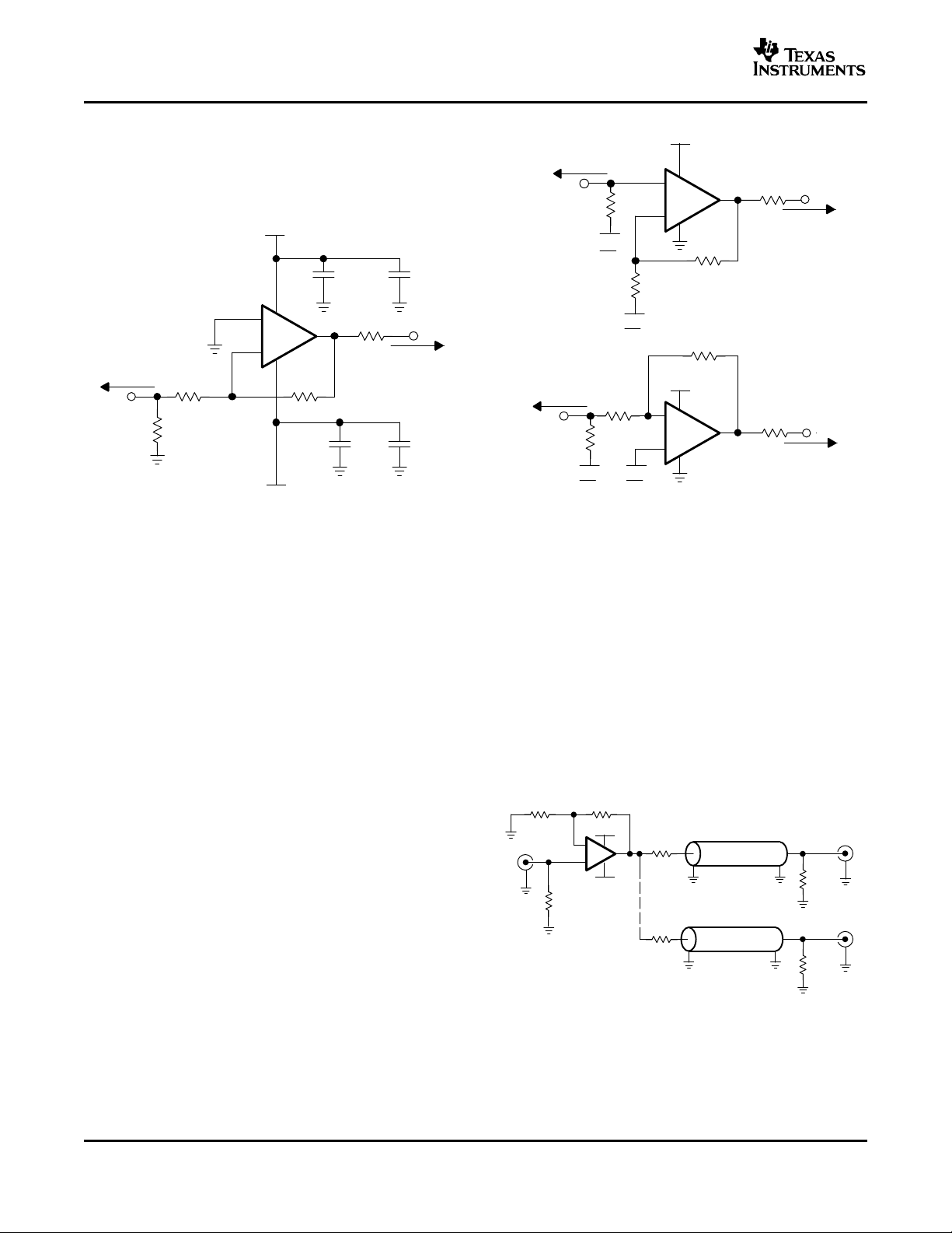
WIDEBAND, INVERTING OPERATION
Figure 46 shows the THS3121 in a typical inverting
gain configuration where the input and output impedances and signal gain from Figure 45 are retained
in an inverting circuit configuration.
Figure 46. Wideband, Inverting Gain
Configuration
SINGLE SUPPLY OPERATION
The THS3120 and THS3121 have the capability to
operate from a single supply voltage ranging from
10 V to 30 V. When operating from a single power
supply, biasing the input and output at mid-supply
allows for the maximum output voltage swing. The
circuits shown in Figure 47 shows inverting and
noninverting amplifiers configured for single supply
operations.
16
Figure 47. DC-Coupled, Single-Supply Operation
Video Distribution
The wide bandwidth, high slew rate, and high output
drive current of the THS3120 and THS3121 matches
the demands for video distribution for delivering video
signals down multiple cables. To ensure high signal
quality with minimal degradation of performance, a
0.1-dB gain flatness should be at least 7x the
passband frequency to minimize group delay variations from the amplifier. A high slew rate minimizes
distortion of the video signal, and supports
component video and RGB video signals that require
fast transition times and fast settling times for high
signal quality.
Figure 48. Video Distribution Amplifier
Application
www.ti.com
0
10
20
30
40
50
60
10 100
C
L
− Capacitive Load − pF
Recommended R Ω
Gain = 5,
RL = 50 Ω,
VS = ±15 V
ISO
Resistance −
_
+
V
S
-V
S
49.9 Ω
499 Ω
5.11 Ω
1 µF
124 Ω
V
S
100 Ω LOAD
R
ISO
_
+
V
S
-V
S
49.9 Ω
5.11 Ω
1 µF
124 Ω
V
S
27 pF
499 Ω
R
F
R
G
750 Ω
100 Ω LOAD
R
IN
_
+
V
S
-V
S
49.9 Ω
499 Ω
Ferrite Bead
1 µF
124 Ω
V
S
100 Ω LOAD
THS3120, THS3121
SLOS420A – SEPTEMBER 2003 – REVISED NOVEMBER 2003
Driving Capacitive Loads
Applications, such as FET drivers and line drivers can
be highly capacitive and cause stability problems for
high-speed amplifiers.
Figure 49 through Figure 55 show recommended
methods for driving capacitive loads. The basic idea
is to use a resistor or ferrite chip to isolate the phase
shift at high frequency caused by the capacitive load
from the amplifier’s feedback path. See Figure 49 for
recommended resistor values versus capacitive load.
Figure 49. Recommended R
vs Capacitive Load
ISO
Placing a small series resistor, R
, between the
ISO
amplifier’s output and the capacitive load, as shown
in Figure 50 , is an easy way of isolating the load
capacitance.
Using a ferrite chip in place of R
, as shown in
ISO
Figure 51 , is another approach of isolating the output
of the amplifier. The ferrite's impedance characteristic
versus frequency is useful to maintain the low frequency load independence of the amplifier while
isolating the phase shift caused by the capacitance at
high frequency. Use a ferrite with similar impedance
to R
, 20 Ω - 50 Ω, at 100 MHz and low impedance
ISO
at dc.
Figure 52 shows another method used to maintain
the low frequency load independence of the amplifier
while isolating the phase shift caused by the capacitance at high frequency. At low frequency, feedback
is mainly from the load side of R
. At high fre-
ISO
quency, the feedback is mainly via the 27-pF capacitor. The resistor R
in series with the negative input
IN
is used to stabilize the amplifier and should be equal
to the recommended value of R
Replacing R
with a ferrite of similar impedance at
IN
F
at unity gain.
about 100 MHz as shown in Figure 53 gives similar
results with reduced dc offset and low frequency
noise. (See the ADDITIONAL REFERENCE MA-
TERIAL section for expanding the usability of cur-
rent-feedback amplifiers.)
Figure 50.
Figure 51.
Figure 52.
17
www.ti.com
_
+
V
S
-V
S
49.9 Ω
5.11 Ω
1 µF
124 Ω
V
S
27 pF
499 Ω
R
F
R
G
FB
100 Ω LOAD
F
IN
_
+
V
S
-V
S
_
+
V
S
-V
S
-V
S
V
S
301 Ω
301 Ω
66.5 Ω
5.11 Ω
5.11 Ω
_
+
V
S
-V
S
499 Ω
5.11 Ω
124 Ω
V
S
_
+
V
S
-V
S
499 Ω
5.11 Ω
124 Ω
24.9 Ω
24.9 Ω
1 nF
THS3120, THS3121
SLOS420A – SEPTEMBER 2003 – REVISED NOVEMBER 2003
Figure 53.
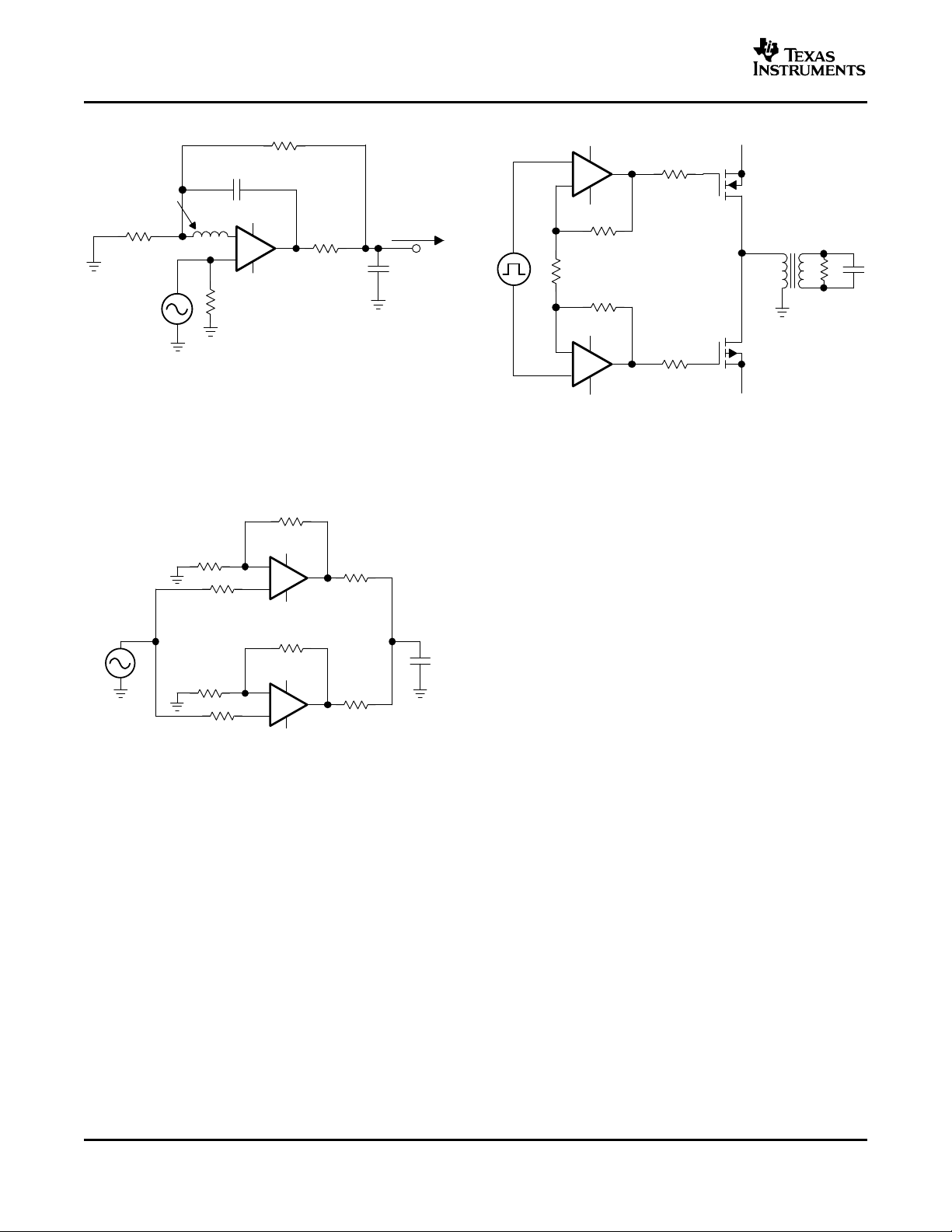
Figure 54 is shown using two amplifiers in parallel to
double the output drive current to larger capacitive
loads. This technique is used when more output
current is needed to charge and discharge the load
faster as when driving large FET transistors.
Figure 54.
Figure 55 shows a push-pull FET driver circuit typical
of ultrasound applications with isolation resistors to
isolate the gate capacitance from the amplifier.
18
Figure 55. PowerFET Drive Circuit
SAVING POWER WITH POWER-DOWN
FUNCTIONALITY AND SETTING
THRESHOLD LEVELS WITH THE
REFERENCE PIN
The THS3120 features a power-down pin (PD) which
lowers the quiescent current from 7 mA down to 300
µA, ideal for reducing system power.
The power-down pin of the amplifier defaults to the
negative supply voltage in the absence of an applied
voltage, putting the amplifier in the power-on mode of
operation. To turn off the amplifier in an effort to
conserve power, the power-down pin can be driven
towards the positive rail. The threshold voltages for
power-on and power-down are relative to the supply
rails and are given in the specification tables. Below
the Enable Threshold Voltage, the device is on.
Above the Disable Threshold Voltage, the device is
off. Behavior in between these threshold voltages is
not specified.
Note that this power-down functionality is just that;
the amplifier consumes less power in power-down
mode. The power-down mode is not intended to
provide a high-impedance output. In other words, the
power-down functionality is not intended to allow use
as a 3-state bus driver. When in power-down mode,
the impedance looking back into the output of the
amplifier is dominated by the feedback and gain
setting resistors, but the output impedance of the
device itself varies depending on the voltage applied
to the outputs.
Figure 56 shows the total system output impedance
which includes the amplifier output impedance in
parallel with the feedback plus gain resistors, which
cumulate to 1298 Ω . Figure 45 shows this circuit
configuration for reference.

www.ti.com
0
200
400
600
800
1000
1200
1400
100 k 1 M 10 M 100 M 1 G
f − Frequency − Hz
Powerdown Output Impedance − Ω
Gain = 2
RF = 649 Ω
VS = ±15 V and ±5 V
Figure 56. Power-down Output Impedance vs
Frequency
As with most current feedback amplifiers, the internal
architecture places some limitations on the system
when in power-down mode. Most notably is the fact
that the amplifier actually turns ON if there is a ± 0.7 V
or greater difference between the two input nodes
(V+ and V-) of the amplifier. If this difference exceeds
± 0.7 V, the output of the amplifier creates an output
voltage equal to approximately
[(V+ - V-) -0.7 V] × Gain. This also implies that if a
voltage is applied to the output while in power-down
mode, the V- node voltage is equal to
V
O(applied)
× R
/(R
+ RG). For low gain configurations
G
F
and a large applied voltage at the output, the amplifier may actually turn ON due to the aforementioned
behavior.
The time delays associated with turning the device on
and off are specified as the time it takes for the
amplifier to reach either 10% or 90% of the final
output voltage. The time delays are in the order of
microseconds because the amplifier moves in and out
of the linear mode of operation in these transitions.
POWER-DOWN REFERENCE PIN
OPERATION
In addition to the power-down pin, the THS3120 also
features a reference pin (REF) which allows the user
to control the enable or disable power-down voltage
levels applied to the PD pin. In most split-supply
applications, the reference pin is connected to
ground. In either case, the user needs to be aware of
voltage level thresholds that apply to the power-down
pin. The usable range at the REF pin is from V
(V
- 4 V).
S+
THS3120, THS3121
SLOS420A – SEPTEMBER 2003 – REVISED NOVEMBER 2003
PRINTED-CIRCUIT BOARD LAYOUT
TECHNIQUES FOR OPTIMAL
PERFORMANCE
Achieving optimum performance with high frequency
amplifiers, like the THS3120 and THS3121, requires
careful attention to board layout parasitic and external
component types.
Recommendations that optimize performance include:
• Minimize parasitic capacitance to any ac ground
for all of the signal I/O pins. Parasitic capacitance
on the output and input pins can cause instability.
To reduce unwanted capacitance, a window
around the signal I/O pins should be opened in all
of the ground and power planes around those
pins. Otherwise, ground and power planes should
be unbroken elsewhere on the board.
• Minimize the distance (< 0.25”) from the power
supply pins to high frequency 0.1- µF and 100-pF
decoupling capacitors. At the device pins, the
ground and power plane layout should not be in
close proximity to the signal I/O pins. Avoid
narrow power and ground traces to minimize
inductance between the pins and the decoupling
capacitors. The power supply connections should
always be decoupled with these capacitors.
Larger (6.8 µF or more) tantalum decoupling
capacitors, effective at lower frequency, should
also be used on the main supply pins. These may
be placed somewhat farther from the device and
may be shared among several devices in the
same area of the PC board.
• Careful selection and placement of external
components preserve the high frequency performance of the THS3120 and THS3121. Resistors should be a very low reactance type.
Surface-mount resistors work best and allow a
tighter overall layout. Again, keep their leads and
PC board trace length as short as possible.
Never use wirebound type resistors in a high
frequency application. Since the output pin and
inverting input pins are the most sensitive to
parasitic capacitance, always position the
feedback and series output resistors, if any, as
close as possible to the inverting input pins and
output pins. Other network components, such as
input termination resistors, should be placed
close to the gain-setting resistors. Even with a
low parasitic capacitance shunting the external
to
S-
resistors, excessively high resistor values can
create significant time constants that can degrade
performance. Good axial metal-film or surface-mount resistors have approximately 0.2 pF
in shunt with the resistor. For resistor values >
2.0 k Ω, this parasitic capacitance can add a pole
and/or a zero that can effect circuit operation.
Keep resistor values as low as possible, consistent with load driving considerations.
19

www.ti.com
DIE
Side View (a)
DIE
End View (b)
Thermal
Pad
Bottom View (c)
THS3120, THS3121
SLOS420A – SEPTEMBER 2003 – REVISED NOVEMBER 2003
• Connections to other wideband devices on the almost impossible to achieve a smooth, stable
board may be made with short direct traces or frequency response. Best results are obtained by
through onboard transmission lines. For short soldering the THS3120 / THS3121 parts directly
connections, consider the trace and the input to onto the board.
the next device as a lumped capacitive load.
Relatively wide traces (50 mils to 100 mils)
should be used, preferably with ground and
power planes opened up around them. Estimate
the total capacitive load and determine if isolation
resistors on the outputs are necessary. Low
parasitic capacitive loads (< 4 pF) may not need
an R
since the THS3120 and THS3121 are
S
nominally compensated to operate with a 2-pF
parasitic load. Higher parasitic capacitive loads
without an RS are allowed as the signal gain
increases (increasing the unloaded phase margin). If a long trace is required, and the 6-dB
signal loss intrinsic to a doubly-terminated transmission line is acceptable, implement a matched
impedance transmission line using microstrip or
stripline techniques (consult an ECL design handbook for microstrip and stripline layout techniques). A 50- Ω environment is not necessary
onboard, and in fact, a higher impedance environment improves distortion as shown in the
distortion versus load plots. With a characteristic
board trace impedance based on board material
and trace dimensions, a matching series resistor
into the trace from the output of the THS3120 /
THS3121 is used as well as a terminating shunt
resistor at the input of the destination device.
Remember also that the terminating impedance is
the parallel combination of the shunt resistor and
the input impedance of the destination device:
this total effective impedance should be set to
match the trace impedance. If the 6-dB attenuation of a doubly terminated transmission line is
unacceptable, a long trace can be
series-terminated at the source end only. Treat
the trace as a capacitive load in this case. This
does not preserve signal integrity as well as a
doubly-terminated line. If the input impedance of
the destination device is low, there is some signal
attenuation due to the voltage divider formed by
the series output into the terminating impedance.
• Socketing a high speed part like the THS3120
and THS3121 is not recommended. The additional lead length and pin-to-pin capacitance
introduced by the socket can create an extremely
troublesome parasitic network which can make it
PowerPAD ™ DESIGN CONSIDERATIONS
The THS3120 and THS3121 are available in a
thermally-enhanced PowerPAD family of packages.
These packages are constructed using a downset
leadframe upon which the die is mounted [see
Figure 57 (a) and Figure 57 (b)]. This arrangement
results in the lead frame being exposed as a thermal
pad on the underside of the package [see Figure 57 (c)]. Because this thermal pad has direct
thermal contact with the die, excellent thermal performance can be achieved by providing a good
thermal path away from the thermal pad. Note that
devices such as the THS312x have no electrical
connection between the PowerPAD and the die.
The PowerPAD package allows for both assembly
and thermal management in one manufacturing operation. During the surface-mount solder operation
(when the leads are being soldered), the thermal pad
can also be soldered to a copper area underneath the
package. Through the use of thermal paths within this
copper area, heat can be conducted away from the
package into either a ground plane or other heat
dissipating device.
The PowerPAD package represents a breakthrough
in combining the small area and ease of assembly of
surface mount with the, heretofore, awkward mechanical methods of heatsinking.
Figure 57. Views of Thermal Enhanced Package
Although there are many ways to properly heatsink
the PowerPAD package, the following steps illustrate
the recommended approach.
20

www.ti.com
0.060
0.040
0.075 0.025
0.205
0.010
vias
Pin 1
Top V iew
0.017
0.035
0.094
0.030
0.013
Figure 58. DGN PowerPAD PCB Etch and Via
Pattern
PowerPAD ™ LAYOUT CONSIDERATIONS
1. PCB with a top side etch pattern as shown in
Figure 58 . There should be etch for the leads as
well as etch for the thermal pad.
2. Place five holes in the area of the thermal pad.
These holes should be 10 mils in diameter. Keep
them small so that solder wicking through the
holes is not a problem during reflow.
3. Additional vias may be placed anywhere along
the thermal plane outside of the thermal pad
area. This helps dissipate the heat generated by
the THS3120 / THS3121 IC. These additional
vias may be larger than the 10-mil diameter vias
directly under the thermal pad. They can be
larger because they are not in the thermal pad
area to be soldered so that wicking is not a
problem.
4. Connect all holes to the internal ground plane.
Note that the PowerPAD is electrically isolated
from the silicon and all leads. Connecting the
PowerPAD to any potential voltage such as V
is acceptable as there is no electrical connection
to the silicon.
5. When connecting these holes to the ground
plane, do not use the typical web or spoke via
connection methodology. Web connections have
THS3120, THS3121
SLOS420A – SEPTEMBER 2003 – REVISED NOVEMBER 2003
a high thermal resistance connection that is
useful for slowing the heat transfer during
soldering operations. This makes the soldering of
vias that have plane connections easier. In this
application, however, low thermal resistance is
desired for the most efficient heat transfer. Therefore, the holes under the THS3120 / THS3121
PowerPAD package should make their connection to the internal ground plane with a complete
connection around the entire circumference of the
plated-through hole.
6. The top-side solder mask should leave the terminals of the package and the thermal pad area
with its five holes exposed. The bottom-side
solder mask should cover the five holes of the
thermal pad area. This prevents solder from
being pulled away from the thermal pad area
during the reflow process.
7. Apply solder paste to the exposed thermal pad
area and all of the IC terminals.
8. With these preparatory steps in place, the IC is
simply placed in position and run through the
solder reflow operation as any standard surface-mount component. This results in a part that
is properly installed.
POWER DISSIPATION AND THERMAL
CONSIDERATIONS
The THS3120 and THS3121 incorporates automatic
thermal shutoff protection. This protection circuitry
shuts down the amplifier if the junction temperature
exceeds approximately 160 ° C. When the junction
temperature reduces to approximately 140 ° C, the
amplifier turns on again. But, for maximum performance and reliability, the designer must take care to
ensure that the design does not exeed a junction
temperature of 125 ° C. Between 125 ° C and 150 ° C,
damage does not occur, but the performance of the
amplifier begins to degrade and long term reliability
suffers. The thermal characteristics of the device are
,
S-
dictated by the package and the PC board. Maximum
power dissipation for a given package can be calculated using the following formula.
21

www.ti.com
P
Dmax
T
max
T
A
JA
where:
P
Dmax
is the maximum power dissipation in the amplifier (W).
T
max
is the absolute maximum junction temperature (°C).
TA is the ambient temperature (°C).
θJA = θ
JC
+ θ
CA
θJC is the thermal coeffiecient from the silicon junctions to
the case (°C/W).
θCA is the thermal coeffiecient from the case to ambient
air (°C/W).
4
3.5
3
2.5
2
1.5
1
0.5
0
−40 −20 0 20 40 60 80 100
− Maximum Power Dissipation − W
P
D
TA − Free-Air Temperature − °C
Results are With No Air Flow and PCB Size = 3”x 3”
θJA = 58.4°C/W for 8-Pin MSOP w/PowerPad (DGN)
θJA = 95°C/W for 8-Pin SOIC High−K Test PCB (D)
θJA = 158°C/W for 8-Pin MSOP w/PowerPad w/o Solder
θJA = 58.4°C/W
θJA = 95°C/W
θJA = 158°C/W
ΤJ = 125°C
THS3120, THS3121
SLOS420A – SEPTEMBER 2003 – REVISED NOVEMBER 2003
For systems where heat dissipation is more critical,
the THS3120 and THS3121 are offered in an 8-pin
MSOP with PowerPAD package offering even better
thermal performance. The thermal coefficient for the
PowerPAD packages are substantially improved over
the traditional SOIC. Maximum power dissipation
levels are depicted in the graph for the available
packages. The data for the PowerPAD packages
assume a board layout that follows the PowerPAD
layout guidelines referenced above and detailed in
the PowerPAD application note (literature number
SLMA002). The following graph also illustrates the
effect of not soldering the PowerPAD to a PCB. The
thermal impedance increases substantially which may
cause serious heat and performance issues. Be sure
to always solder the PowerPAD to the PCB for
optimum performance.
When determining whether or not the device satisfies
the maximum power dissipation requirement, it is
important to not only consider quiescent power dissipation, but also dynamic power
dissipation. Often times, this is difficult to quantify
because the signal pattern is inconsistent, but an
estimate of the RMS power dissipation can provide
visibility into a possible problem.
DESIGN TOOLS
Evaluation Fixtures, Spice Models, and
Application Support
Texas Instruments is committed to providing its customers with the highest quality of applications support. To support this goal an evaluation board has
been developed for the THS3120 and THS3121
operational amplifier. The board is easy to use,
allowing for straightforward evaluation of the device.
The evaluation board can be ordered through the
Texas Instruments web site, www.ti.com, or through
your local Texas Instruments sales representative.
Computer simulation of circuit performance using
SPICE is often useful when analyzing the performance of analog circuits and systems. This is particularly true for video and RF-amplifier circuits where
parasitic capacitance and inductance can have a
major effect on circuit performance. A SPICE model
for the THS3121 is available through the Texas
Instruments web site (www.ti.com). The PIC is also
available for design assistance and detailed product
information. These models do a good job of predicting small-signal ac and transient performance
under a wide variety of operating conditions. They are
not intended to model the distortion characteristics of
the amplifier, nor do they attempt to distinguish
between the package types in their small-signal ac
performance. Detailed information about what is and
is not modeled is contained in the model file itself.
Figure 59. Maximum Power Distribution vs
22
Ambient Temperature

www.ti.com
TP2GND
J2
+
C2
VS−
J7
C4
C6
C1
J1
+
FB1
C5
C3
FB2
VS−
VS+
VS+
R4
J4
Vin+
R8A
2
3
6
7
4
1
J8
Vs+
R2
Z2
J7
R1
J6
Vout
Vs−
R3
J5
Vin
−
_
+
PD
8
R8B
R5 Z1
TP1
R6
0
R7BR7A
REF
1
THS3120DGN EVM
6445588
THS3120, THS3121
SLOS420A – SEPTEMBER 2003 – REVISED NOVEMBER 2003
NOTE: The Edge number for the THS3121 is
6445589.
Figure 60. THS3120 EVM Circuit Configuration
Figure 61. THS3120 EVM Board Layout
(Top Layer)
Figure 62. THS3120 EVM Board Layout
(Bottom Layer)
23

www.ti.com
THS3120, THS3121
SLOS420A – SEPTEMBER 2003 – REVISED NOVEMBER 2003
Table 2. Bill of Materials
THS3120DGN and THS3121DGN EVM
ITEM DESCRIPTION SMD SIZE
1 BeadD, Ferrite, 3 A, 80 Ω 1206 FB1, FB2 2 (Steward) HI1206N800R-00
2 Cap. 6.8 µF, Tanatalum, 35 V, 10% D C1, C2 2 (AVX) TAJD685K035R
3 Open 0805 R5, Z1 2
4 Cap. 0.1 µF, Ceramic, X7R, 50 V 0805 C3, C4 2 (AVX) 08055C104KAT2A
5 Cap. 100 pF, Ceramic, NPO, 100 V 0805 C5, C6 2 (AVX) 08051A101JAT2A
6 Resistor, 0 Ω , 1/8 W, 1% 0805 R6
7 Resistor, 124 Ω , 1/8 W, 1% 0805 R3 1 (Phycomp) 9C08052A1240FKHFT
8 Resistor, 499 Ω , 1/8 W, 1% 0806 R4 1 (Phycomp) 9C08052A4990FKHFT
9 Open 1206 R7A, Z2 2
10 Resistor, 49.9 Ω , 1/4 W, 1% 1206 R2, R8A 2 (Phycomp) 9C12063A49R9FKRFT
11 Resistor, 0 Ω , 1/4 W, 1% 1206 R1 1 (Phycomp) 9C12063A53R6FKRFT
12 Open 2512 R7B, R8B 2
13 Header, 0.1" CTRS, 0.025" SQ pins 3 Pos. JP1
14 Shunts JP1
15 J1, J2, J3 3 (SPC) 813
16 Test point, red J7
17 Test point, black TP2 1 (Keystone) 5001
18 Connector, SMA PCB jack J4, J5, J6 3 (Amphenol) 901-144-8RFX
19 Standoff, 4-40 hex, 0.625" length 4 (Keystone) 1808
20 Screw, Phillips, 4-40, 0.250" 4 SHR-0440-016-SN
21 IC, THS3120 U1
22 Board, printed-circuit (THS3120)
23 IC, THS3121 U1 1 (TI) THS3121DGN
24 Board, printed-circuit (THS3121) 1 (TI) EDGE # 6445589
Jack, banana receptance, 0.25" dia.
hole
(1) The manufacturer's part numbers were used for test purposes only.
(2) Applies to the THS3120DGN EVM only.
REFERENCE PCB MANUFACTURER'S
DESIGNATOR QUANTITY PART NUMBER
(2)
(2)
(2)
(2)
(2)
, J8
, TP1 3 (Keystone) 5000
(2)
(2)
1 (Phycomp) 9C08052A0R00JLHFT
1 (Sullins) PZC36SAAN
1 (Sullins) SSC02SYAN
1 (TI) THS3120DGN
1 (TI) EDGE # 6445588
(1)
ADDITIONAL REFERENCE MATERIAL
• PowerPAD Made Easy, application brief (SLMA004)
• PowerPAD Thermally Enhanced Package, technical brief (SLMA002)
• Voltage Feedback vs Current Feedback Amplifiers, (SLVA051)
• Current Feedback Analysis and Compensation (SLOA021)
• Current Feedback Amplifiers: Review, Stability, and Application (SBOA081)
• Effect of Parasitic Capacitance in Op Amp Circuits (SLOA013)
• Expanding the Usability of Current-Feedback Amplifiers, by Randy Stephens, 3Q 2003 Analog Applications
Journal www.ti.com/sc/analogapps).
24

THERMAL PAD MECHANICAL DATA
www.ti.com
DGN (S-PDSO-G8)
THERMAL INFORMATION
This PowerPAD™ package incorporates an exposed thermal pad that is designed to be attached directly to an
external heatsink. When the thermal pad is soldered directly to the printed circuit board (PCB), the PCB can be
used as a heatsink. In addition, through the use of thermal vias, the thermal pad can be attached directly to a
ground plane or special heatsink structure designed into the PCB. This design optimizes the heat transfer from
the integrated circuit (IC).
For additional information on the PowerPAD package and how to take advantage of its heat dissipating abilities,
refer to Technical Brief, PowerPAD Thermally Enhanced Package, Texas Ins truments Literature No. SLMA002
and Application Brief, PowerPAD Made Easy, Texas Instruments Literature N o . SLMA004. Both documents are
available at www.ti.com.
The exposed thermal pad dimensions for this package are shown in the following illustration.
8
5
Exposed Thermal Pad
1,73
MAX
NOTE: All linear dimensions are in millimeters
Exposed Thermal Pad Dimensions
1
1,78
MAX
Top View
4
PPTD041
PowerPAD is a trademark of Texas Instruments


IMPORTANT NOTICE
Texas Instruments Incorporated and its subsidiaries (TI) reserve the right to make corrections, modifications,
enhancements, improvements, and other changes to its products and services at any time and to discontinue
any product or service without notice. Customers should obtain the latest relevant information before placing
orders and should verify that such information is current and complete. All products are sold subject to TI’s terms
and conditions of sale supplied at the time of order acknowledgment.
TI warrants performance of its hardware products to the specifications applicable at the time of sale in
accordance with TI’s standard warranty. Testing and other quality control techniques are used to the extent TI
deems necessary to support this warranty . Except where mandated by government requirements, testing of all
parameters of each product is not necessarily performed.
TI assumes no liability for applications assistance or customer product design. Customers are responsible for
their products and applications using TI components. To minimize the risks associated with customer products
and applications, customers should provide adequate design and operating safeguards.
TI does not warrant or represent that any license, either express or implied, is granted under any TI patent right,
copyright, mask work right, or other TI intellectual property right relating to any combination, machine, or process
in which TI products or services are used. Information published by TI regarding third-party products or services
does not constitute a license from TI to use such products or services or a warranty or endorsement thereof.
Use of such information may require a license from a third party under the patents or other intellectual property
of the third party, or a license from TI under the patents or other intellectual property of TI.
Reproduction of information in TI data books or data sheets is permissible only if reproduction is without
alteration and is accompanied by all associated warranties, conditions, limitations, and notices. Reproduction
of this information with alteration is an unfair and deceptive business practice. TI is not responsible or liable for
such altered documentation.
Resale of TI products or services with statements different from or beyond the parameters stated by TI for that
product or service voids all express and any implied warranties for the associated TI product or service and
is an unfair and deceptive business practice. TI is not responsible or liable for any such statements.
Following are URLs where you can obtain information on other Texas Instruments products and application
solutions:
Products Applications
Amplifiers amplifier.ti.com Audio www.ti.com/audio
Data Converters dataconverter.ti.com Automotive www.ti.com/automotive
DSP dsp.ti.com Broadband www.ti.com/broadband
Interface interface.ti.com Digital Control www.ti.com/digitalcontrol
Logic logic.ti.com Military www.ti.com/military
Power Mgmt power.ti.com Optical Networking www.ti.com/opticalnetwork
Microcontrollers microcontroller.ti.com Security www.ti.com/security
Telephony www.ti.com/telephony
Video & Imaging www.ti.com/video
Wireless www.ti.com/wireless
Mailing Address: Texas Instruments
Post Office Box 655303 Dallas, Texas 75265
Copyright 2004, Texas Instruments Incorporated

Copyright © Each Manufacturing Company.
All Datasheets cannot be modified without permission.
This datasheet has been download from :
www.AllDataSheet.com
100% Free DataSheet Search Site.
Free Download.
No Register.
Fast Search System.
www.AllDataSheet.com
 Loading...