

查询THS1060供应商
THS1060
10-BIT 60 MSPS IF SAMPLING COMMUNICATIONS
ANALOG-TO-DIGITAL CONVERTER
SLAS212 – MARCH 2000
features
D
60 MSPS Maximum Sample Rate
D
10-Bit Resolution
D
No Missing Codes
D
On-Chip Sample and Hold
D
73 dB Spurious Free Dynamic Range at
fin = 15.5 MHz
D
5 V Analog and Digital Supply
D
3 V and 5 V CMOS Compatible Digital
Output
D
9.5 Bit ENOB at fIN = 31 MHz
D
60 dB SNR at fIN = 31 MHz
D
82 MHz Bandwidth
D
Internal or External Reference
D
Buffered 900 Ω Differential Analog Input
applications
D
Wireless Local Loop
D
Wireless Internet Access
D
Cable Modem Receivers
D
Medical Ultrasound
D
Magnetic Resonant Imaging
description
The THS1060 is a high speed low noise 10-bit CMOS pipelined analog-to-digital converter. A dif ferential sample
and hold minimizes even order harmonics and allows for a high degree of common mode rejection at the analog
input. A buffered analog input allows for operation with a constant analog input impedance, and prevents
transient voltage spikes from feeding backward to the analog input source. Full temperature DNL performance
allows for industrial application with the assurance of no missing codes. The THS1060 can operate with either
internal or external references. Internal reference usage selection is accomplished simply by externally
connecting reference output terminals to reference input terminals. Packaged in a small 48-pin quad flat-pack,
the THS1060 makes use of Texas Instruments PowerPAD technology. The die of the THS1060 is bonded
directly to a copper alloy plate which is exposed on the bottom of the package. When soldered to a ground land,
the PowerPAD provides superior heat dissipation and thermal performance ideal for industrial applications
in high temperature environments.
Please be aware that an important notice concerning availability, standard warranty, and use in critical applications of
Texas Instruments semiconductor products and disclaimers thereto appears at the end of this data sheet.
PowerPAD is a trademark of Texas Instruments.
PRODUCTION DATA information is current as of publication date.
Products conform to specifications per the terms of Texas Instruments
standard warranty. Production processing does not necessarily include
testing of all parameters.
POST OFFICE BOX 655303 • DALLAS, TEXAS 75265
Copyright 2000, Texas Instruments Incorporated
1
THS1060
10-BIT 60 MSPS IF SAMPLING COMMUNICATIONS
ANALOG-TO-DIGITAL CONVERTER
SLAS212 – MARCH 2000
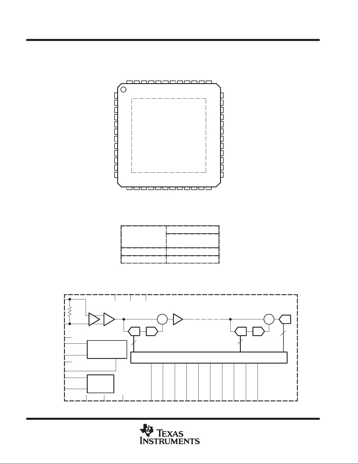
48 PHP PACKAGE
(TOP VIEW)
AV
AV
AV
V
REFOUT–
V
REFIN
V
REFIN
V
REFOUT
AV
AV
DD
DD
CM
V
47 46 45 44 4348 42
1
SS
2
DD
V
3
IN+
V
4
IN–
5
DD
6
–
7
+
8
+
9
V
10
BG
11
SS
12
DD
14 15
13
AV
AVSSAVSSAVDDAV
AV
17 18 19 20
16
SS
DRVSSAVSSDRV
40 39 3841
22 23 24
21
SS
DRVDDDRV
37
DD
36
35
34
33
32
31
30
29
28
27
26
25
NC
NC
D0
D1
D2
D3
D4
D5
D6
D7
D8
D9
functional block diagram
V
V
REFIN+
V
REFOUT+
V
REFOUT–
V
REFIN–
CLK+
CLK–
IN+
V
IN–
V
CM
Buffer
900 Ω
3.0 V
Reference
2.0 V
Timing
AVDDDV
S/H
AV
DD/2
SS
SS
CLK–
CLK+
AV
DV
T
–40°C to 85°C THS1060I
0°C to 70°C THS1060C
DRV
DD
DVDDDVSSDVSSDVDDDVSSDV
AVAILABLE OPTIONS
A
DD
Stage 1 Stage 10
DD
PACKAGE
48-TQFP
(PHP)
Stages 2 – 9
Σ
D/AA/D A/D
1
Digital Error Correction
DRV
SS
DD
DRV
A/D
Σ
D/A
1
1
SS
DV
SS
DRV
SS
POST OFFICE BOX 655303 • DALLAS, TEXAS 75265
AV
2
D9 D8 D7 D6 D5 D4 D3 D2 D1 D0
10-BIT 60 MSPS IF SAMPLING COMMUNICATIONS
I/O
DESCRIPTION
ANALOG-TO-DIGITAL CONVERTER
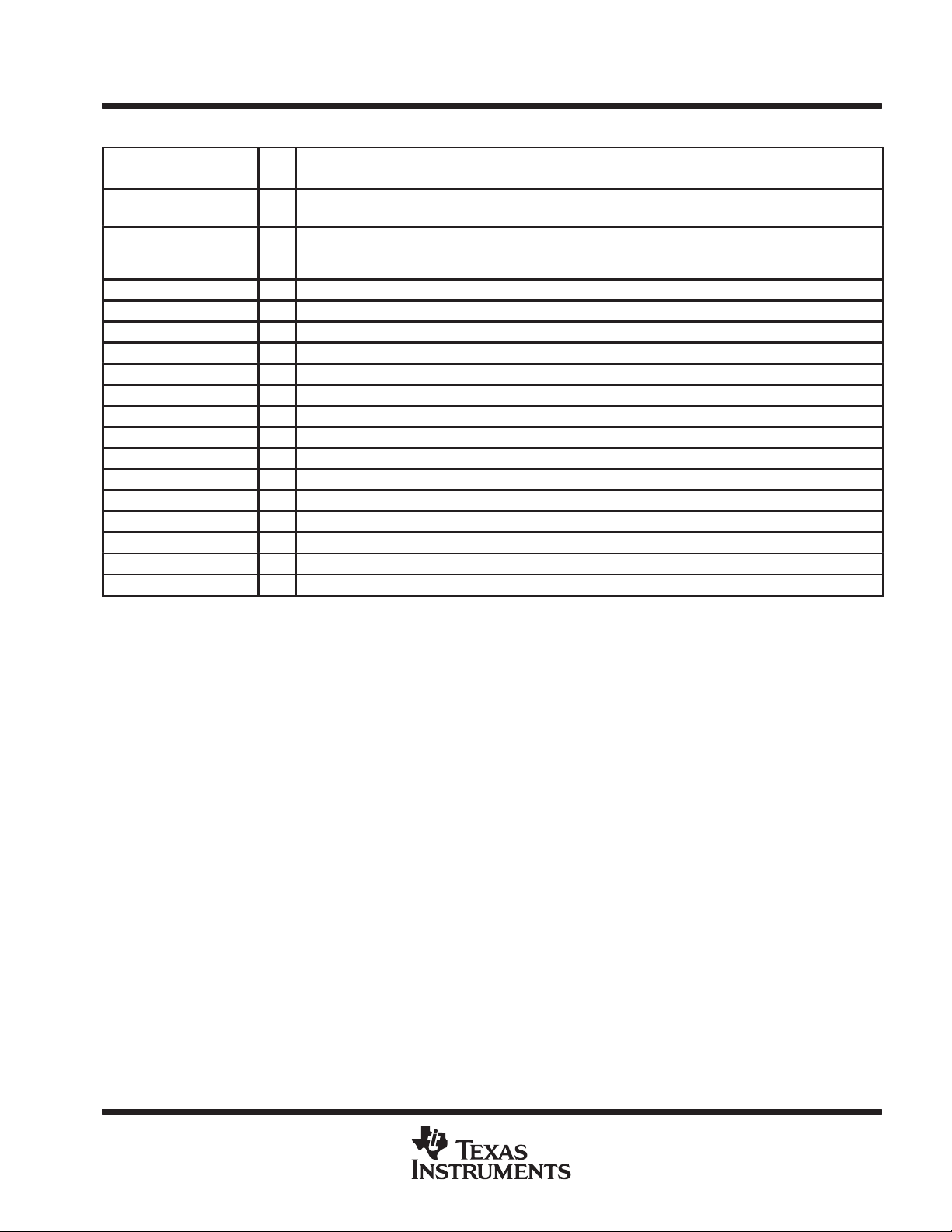
Terminal Functions
TERMINAL
NAME NO.
AV
DD
AV
SS
CLK+ 15 I Clock input
CLK– 16 I Complementary clock input
D9–D0 25–34 O Digital data output bits; LSB= D0, MSB = D9 (2s complement output format)
DRV
DD
DRV
SS
DV
DD
DV
SS
V
BG
V
CM
V
IN+
V
IN–
V
REFIN–
V
REFIN+
V
REFOUT+
V
REFOUT–
2, 5, 12
43, 45, 47
1, 11, 13,
41, 42, 44,
46
24, 37, 38 I Digital output driver supply
23, 39, 40 I Digital output driver ground return
17, 20, 22 I Positive digital supply
18, 19, 21 I Digital ground return
10 O Band gap reference. Bypass to ground with a 1 µF and a 0.01 µF chip capacitor.
48 O Common mode voltage output. Bypass to ground with a 0.1 µF and a 0.01 µF chip device capacitor.
3 I Analog signal input
4 I Complementary analog signal input
7 I External reference input low
8 I External reference input high
9 O Internal reference output. Compensate with a 1 µF and a 0.01 µF chip capacitor.
6 O Internal reference output. Compensate with a 1 µF and a 0.01 µF chip capacitor.
I Analog power supply
I Analog ground return for internal analog circuitry
THS1060
SLAS212 – MARCH 2000
detailed description
The THS1060 uses a differential pipeline architecture and assures no missing codes over the full operating
temperature range. The device uses a 1 bit per stage architecture in order to achieve the highest possible
bandwidth. The differential analog inputs are terminated with a 900 Ω resistor . The inputs are then fed to a unity
gain buffer followed by the S/H (sample and hold) stage. This S/H stage is a switched capacitor op-amp based
circuit, see Figure 3. The pipeline is a typical 1 bit per stage pipeline as shown in the functional block diagram.
The digital output of the 10 stages and the last 1 bit flash are sent to a digital correction logic block which then
outputs the final 10 bits.
POST OFFICE BOX 655303 • DALLAS, TEXAS 75265
3
THS1060
10-BIT 60 MSPS IF SAMPLING COMMUNICATIONS
ANALOG-TO-DIGITAL CONVERTER
SLAS212 – MARCH 2000
absolute maximum ratings over operating free-air temperature (unless otherwise noted)
†
Supply voltage range: AVDD –0.5 V to 7 V. . . . . . . . . . . . . . . . . . . . . . . . . . . . . . . . . . . . . . . . . . . . . . . . . . . . . . . .
DVDD –0.5 V to 7 V. . . . . . . . . . . . . . . . . . . . . . . . . . . . . . . . . . . . . . . . . . . . . . . . . . . . . . . .
DRVDD –0.5 V to 7 V. . . . . . . . . . . . . . . . . . . . . . . . . . . . . . . . . . . . . . . . . . . . . . . . . . . . . .
Voltage between AV
and DVSS –0.3 V to 0.5 V. . . . . . . . . . . . . . . . . . . . . . . . . . . . . . . . . . . . . . . . . . . . . . . . . . .
SS
Voltage between DRVDD and DVDD –0.5 V to 5 V. . . . . . . . . . . . . . . . . . . . . . . . . . . . . . . . . . . . . . . . . . . . . . . . . .
Voltage between AVDD and DVDD –0.5 V to 5 V. . . . . . . . . . . . . . . . . . . . . . . . . . . . . . . . . . . . . . . . . . . . . . . . . . .
Digital data output –0.3 V to DVDD+0.3 V. . . . . . . . . . . . . . . . . . . . . . . . . . . . . . . . . . . . . . . . . . . . . . . . . . . . . . . . . .
CLK peak input current 20 mA. . . . . . . . . . . . . . . . . . . . . . . . . . . . . . . . . . . . . . . . . . . . . . . . . . . . . . . . . . . . . . . . . . .
Peak total input current (all inputs) –30 mA. . . . . . . . . . . . . . . . . . . . . . . . . . . . . . . . . . . . . . . . . . . . . . . . . . . . . . . .
Operating free-air temperature range, TA: THS1060C 0°C to 70°C. . . . . . . . . . . . . . . . . . . . . . . . . . . . . . . . . . . .
THS1060I –40°C to 85°C. . . . . . . . . . . . . . . . . . . . . . . . . . . . . . . . . .
Storage temperature range –65°C to 150°C. . . . . . . . . . . . . . . . . . . . . . . . . . . . . . . . . . . . . . . . . . . . . . . . . . . . . . . .
Lead temperature 1,6 mm (1/16 inch) from the case for 10 seconds 260°C. . . . . . . . . . . . . . . . . . . . . . . . . . . .
†
Stresses beyond those listed under “absolute maximum ratings” may cause permanent damage to the device. These are stress ratings only, and
functional operation of the device at these or any other conditions beyond those indicated under “recommended operating conditions” is not
implied. Exposure to absolute-maximum-rated conditions for extended periods may affect device reliability.
recommended operating conditions
PARAMETER MIN NOM MAX UNIT
Sample rate 1 60 MSPS
Analog supply voltage, AV
Digital supply voltage, DV
Digital output driver supply voltage, DRV
CLK + high level input voltage, V
CLK + low-level input voltage, V
CLK – high-level input voltage, V
CLK – low-level input voltage, V
CLK pulse-width high, t
CLK pulse-width low, t
Operating free-air temperature range, T
Operating free-air temperature range, T
DD
DD
IH
IL
IH
IL
p(H)
p(L)
DD
THS1060C 0 70 °C
A
THS1060I –40 85 °C
A
4.75 5 5.25 V
4.75 5 5.25 V
3 3.3 5.25 V
4 5 5.5 V
0 1 V
4 5 5.5 V
0 1 V
7.5 8.3 ns
7.5 8.3 ns
electrical characteristics, over recommended operating free-air temperature range,
AV
= DVDD = 5 V, DRVDD = 3.3 V, internal references, CLK = 60 MHz, (unless otherwise noted)
DD
dc accuracy
PARAMETER TEST CONDITIONS MIN TYP MAX UNIT
DNL Dif ferential nonlinearity (see Note 1) ±0.4 ±1 LSB
No missing codes (see Note 2) Assured
INL Integral nonlinearity (see Note 1) ±0.9 ±3 LSB
E
O
E
G
‡
All typical values are at TA = 25°C.
NOTES: 1. Tested without over ranging
4
Offset error 15 31 mV
Gain error –7 –10 %FSR
2. Tested with over ranging
POST OFFICE BOX 655303 • DALLAS, TEXAS 75265
‡
THS1060
10-BIT 60 MSPS IF SAMPLING COMMUNICATIONS
ANALOG-TO-DIGITAL CONVERTER
SLAS212 – MARCH 2000
electrical characteristics, over recommended operating free-air temperature range,
= DVDD = 5 V, DRVDD = 3.3 V, internal references, CLK = 60 MHz, (unless otherwise noted)
AV
DD
power supply
PARAMETER TEST CONDITIONS MIN TYP MAX UNIT
I(AV
I(DV
I(DRV
P
D
†
All typical values are at TA = 25°C.
reference
V
REFOUT–
V
REFOUT+
V
REFIN–
V
REFIN+
V(VCM) Common mode output voltage AVDD/2 V
I(VCM) Common mode output current 10 µA
†
All typical values are at TA = 25°C.
Analog supply current V(VIN) = V(VCM) 120 150 mA
DD)
Digital supply current V(VIN) = V(VCM) 2 5 mA
DD)
Output driver supply current V(VIN) = V(VCM) 2 6 mA
DD)
Power dissipation V(VIN) = V(VCM) 0.6 W
PARAMETER TEST CONDITIONS MIN TYP MAX UNIT
Negative reference output voltage 1.95 2 2.05 V
Positive reference output voltage 2.95 3 3.05 V
External reference supplied 2 V
External reference supplied 3 V
†
analog input
PARAMETER TEST CONDITIONS MIN TYP MAX UNIT
RIDifferential input resistance 900 Ω
CIDifferential input capacitance 4 pF
VIAnalog input common mode range VCM ±0.05 V
VIDDifferential input voltage range 2
BW Analog input bandwidth (large signal) –3 dB 82 MHz
†
All typical values are at TA = 25°C.
V p-p
digital outputs
PARAMETER TEST CONDITIONS MIN TYP MAX UNIT
V
OH
V
OL
C
L
†
All typical values are at TA = 25°C.
High-level output voltage IOH = –50 µA 0.8DRV
Low-level output voltage IOL = 50 µA 0.2DRV
Output load capacitance 15 pF
DD
DDVDD
V
POST OFFICE BOX 655303 • DALLAS, TEXAS 75265
5
THS1060
dBc
d
d
10-BIT 60 MSPS IF SAMPLING COMMUNICATIONS
ANALOG-TO-DIGITAL CONVERTER
SLAS212 – MARCH 2000
ac specifications, over recommended operating free-air temperature range, AVDD = DVDD = 5 V,
DRV
noted)
SNR Signal to noise ratio
SINAD Signal to noise and distortion
ENOB Effective number of bits fIN =15.5 MHz 8.5 9.6 bits
THD Total harmonic distortion fIN =15.5 MHz –72 –54
SFDR Spurious-free dynamic range fIN =15.5 MHz 57 73
2
3
Two tone SFDR
†
All typical values are at TA = 25°C.
= 3.3 V, internal references, CLK = 60 MHz, analog input at – 2 dBFS(unless otherwise
DD
†
PARAMETER TEST CONDITIONS MIN TYP MAX UNIT
fIN = 2.2 MHz 60
n
Harmonic Distortion
r
Harmonic Distortion
fIN =15.5 MHz
fIN =31 MHz 60
fIN = 2.2 MHz 59
fIN =15.5 MHz
fIN =31 MHz 59
fIN = 2.2 MHz –80
fIN =15.5 MHz
fIN = 31 MHz –79
fIN = 2.2 MHz –68
fIN =15.5 MHz
fIN = 31 MHz –68
F1 = 14.9 MHz, F2 = 15.6 MHz,
Analog inputs at – 8 dBFS each
56 60
53 59.6
–77 –57
–79 –60
70 dBc
dBFS
dBFS
dBc
dBc
operating characteristics over recommended operating conditions, AVDD = DVDD = 5 V,
DRV
DD = 3.3 V
switching specifications
PARAMETER TEST CONDITIONS MIN TYP MAX UNIT
Aperture delay, t
Aperture jitter 1 ps RMS
Output delay t
Pipeline delay t
d(A)
d(O)
d(PIPE)
After falling edge of CLK+ 13 ns
120 ps
6.5
CLK
Cycle
6
POST OFFICE BOX 655303 • DALLAS, TEXAS 75265

10-BIT 60 MSPS IF SAMPLING COMMUNICATIONS
ANALOG-TO-DIGITAL CONVERTER
SLAS212 – MARCH 2000
definitions of specifications
analog bandwidth
The analog input frequency at which the spectral power of the fundamental frequency of a large input signal
is reduced by 3 dB.
aperture delay
The delay between the 50% point of the rising edge of the clock and the instant at which the analog input is
sampled.
aperture uncertainity (jitter)
The sample-to-sample variation in aperture delay
differential nonlinearity
The average deviation of any output code from the ideal width of 1 LSB.
clock pulse width/duty cycle
Pulse width high is the minimum amount of time that the clock pulse should be left in logic 1 state to achieve
rated performance; pulse width low is the minimum time clock pulse should be left in low state. At a given clock
rate, these specs define acceptable clock duty cycles.
offset error
The difference between the analog input voltage at which the analog-to-digital converter output changes from
negative full scale, to one LSB above negative full scale, and the ideal voltage at which this transition should
occur.
THS1060
gain error
The maximum error in LSBs between a digitized ideal full scale low frequency offset corrected triangle wave
analog input, from the ideal digitized full scale triangle wave, divided by the full scale range, in this case 1024.
harmonic distortion
The ratio of the power of the fundamental to a given harmonic component reported in dBc.
integral nonlinearity
The deviation of the transfer function from an end-point adjusted reference line measured in fractions of 1 LSB.
Also the integral of the DNL curve.
output delay
The delay between the 50% point of the falling edge of the clock and signal and the time when all output data
bits are within valid logic levels (not including pipeline delay).
signal-to-noise-and distortion (SINAD)
When tested with a single tone, the ratio of the signal power to the sum of the power of all other spectral
components, excluding dc, referenced to full scale.
signal-to-noise ratio (SNR)
When tested with a single tone, the ratio of the signal power to the sum of the power of all other power spectral
components, excluding dc and the first 9 harmonics, referenced to full scale.
effective number of bits (ENOB)
For a sine wave, SINAD can be expressed in terms of the number of bits, using the following formula,
ENOB
(
SINAD*1.76
+
6.02
)
spurious-free dynamic range (SFDR)
The ratio of the signal power to the power of the worst spur, excluding dc. The worst spurious component may
or may not be a harmonic. The ratio is reported in dBc (that is, degrades as signal levels are lowered).
POST OFFICE BOX 655303 • DALLAS, TEXAS 75265
7

THS1060
10-BIT 60 MSPS IF SAMPLING COMMUNICATIONS
ANALOG-TO-DIGITAL CONVERTER
SLAS212 – MARCH 2000
Sample N
AIN
t
d(A)
tp(H) tP(L)
t
d(Pipe)
CLK+
Digital Output
(D0 – D9)
Data N–7
equivalent circuits
BAND
GAP
R1
R1
t
c
Data N–6 Data N–5 Data N–4 Data N–3 Data N–2 Data N–1 Data N Data N+1 Data N+2
t
d(O)
Figure 1. Timing Diagram
R2
V
V
REFOUT+
V
REFOUT–
R2
AV
DD
R
1
V
CM
R
2
AV
SS
VIN+
VIN–
φ1
900 Ω
φ1
V
Figure 3. Analog Input Stage
φ2
CM
φ1′
φ1′
CM
φ2
Figure 2. References
DV
CLK+
DV
SS
DV
CLK–
DV
SS
Figure 4. Clock Inputs
DD
DD
Timing
V
DD
10 Ω
V
SS
Figure 5. Digital Outputs
D0–D11
8
POST OFFICE BOX 655303 • DALLAS, TEXAS 75265

THS1060
10-BIT 60 MSPS IF SAMPLING COMMUNICATIONS
ANALOG-TO-DIGITAL CONVERTER
SLAS212 – MARCH 2000
0
–10
–20
–30
–40
–50
–60
–70
Power – dBFS
–80
–90
–100
–110
0 5 10 15 20 25 30
TYPICAL CHARACTERISTICS
OUTPUT POWER SPECTRUM
vs
FREQUENCY
Fs = 60 MSPS
fIN = 2.2 MHz, VIN @ –2 dBFS
8K Point Discrete Fourier
Transform
f – Frequency – MHz
Figure 6
OUTPUT POWER SPECTRUM
vs
FREQUENCY
†
0
–10
–20
–30
–40
–50
–60
–70
Power – dBFS
–80
–90
–100
–110
0 5 10 15 20 25 30
f – Frequency – MHz
Figure 7
†
AVDD = 5 V, DVDD = 5 V, DRVDD = 3.3 V, TA = 25°C (unless otherwise noted)
Fs = 60 MSPS
fIN = 15.5 MHz, VIN @ –2 dBFS
8K Point Discrete Fourier
Transform
POST OFFICE BOX 655303 • DALLAS, TEXAS 75265
9

THS1060
10-BIT 60 MSPS IF SAMPLING COMMUNICATIONS
ANALOG-TO-DIGITAL CONVERTER
SLAS212 – MARCH 2000
TYPICAL CHARACTERISTICS
OUTPUT POWER SPECTRUM
vs
FREQUENCY
0.00
–10.00
–20.00
–30.00
–40.00
–50.00
–60.00
–70.00
Power – dBFS
–80.00
–90.00
–100.00
–110.00
Fs = 60 MSPS
fIN = 31 MHz, VIN @ –2 dBFS
8K Point Discrete Fourier
Transform
0 5 10 15 20 25 30
f – Frequency – MHz
Figure 8
OUTPUT POWER SPECTRUM
vs
FREQUENCY
0
–10
–20
–30
–40
–50
–60
–70
Power – dBFS
–80
–90
–100
–110
0 5 10 15 20 25 30
f – Frequency – MHz
Fs = 60 MSPS
fIN = 69 MHz, VIN @ –2 dBFS
8K Point Discrete Fourier
Transform
Figure 9
10
POST OFFICE BOX 655303 • DALLAS, TEXAS 75265

10-BIT 60 MSPS IF SAMPLING COMMUNICATIONS
ANALOG-TO-DIGITAL CONVERTER
TYPICAL CHARACTERISTICS
NOISE AND DISTORTION
vs
ANALOG INPUT FREQUENCY
100
90
80
70
60
50
40
Power – dB
30
20
10
0
0 102030405060708090100
2nd
Harmonic
(dBc)
SFDR (dBc)
3rd
Harmonic
(dBc)
f – Analog Input Frequency – MHz
Figure 10
Fs = 60 MSPS
VIN @ –2 dBFS
SINAD
(dBFS)
SNR (dBFS)
THS1060
SLAS212 – MARCH 2000
TWO-TONE OUTPUT POWER SPECTRUM
vs
FREQUENCY
0
–10
–20
–30
–40
–50
–60
–70
Power – dBFS
–80
–90
–100
–110
0 5 10 15 20 25 30
f – Frequency – MHz
Fs=60 MSPS, F1=14.9 MHz,
F2 = 15.6 MHz each @ –8 dBFS
8K Point Discrete Fourier
Transform
Figure 11
POST OFFICE BOX 655303 • DALLAS, TEXAS 75265
11

THS1060
10-BIT 60 MSPS IF SAMPLING COMMUNICATIONS
ANALOG-TO-DIGITAL CONVERTER
SLAS212 – MARCH 2000
TYPICAL CHARACTERISTICS
NOISE AND DISTORTION
vs
ANALOG INPUT POWER LEVEL
100
90
Fs = 60 MSPS
fIN = 15.5 MHz
80
70
60
50
40
Power – dB
30
20
10
0
–50 –45 –40 –35 –30 –25 –20 –15 –10 –5 0
SNR(dBFS)
Input Power – dBFS
Figure 12
SFDR(dBc)
SINAD(dBFS)
NOISE AND DISTORTION
vs
CLOCK FREQUENCY
100
90
80
70
60
50
40
Power – dB
30
20
10
fIN = 15.5 MHz, VIN @ –2 dBFS
0
5 1015202530354045505560657075
SFDR(dBc)
SINAD(dBFS)
Clock Frequency – MHz
SNR(dBFS)
Figure 13
12
POST OFFICE BOX 655303 • DALLAS, TEXAS 75265

10-BIT 60 MSPS IF SAMPLING COMMUNICATIONS
ANALOG-TO-DIGITAL CONVERTER
TYPICAL CHARACTERISTICS
NOISE AND DISTORTION
vs
DUTY CYCLE
100
90
80
70
60
50
40
Power – dB
30
Fs = 60 MSPS
20
fIN = 15.5 MHz, VIN @ –2 dBFS
PowerPAD not connected, T = 25°C
10
0
40 45 50 55 60
SFDR (dBc)
SINAD (dBFS)
Duty Cycle – %
Figure 14
SNR (dBFS)
THS1060
SLAS212 – MARCH 2000
DIFFERENTIAL NONLINEARITY
vs
OUTPUT CODE
1
Fs = 60 MSPS
fIN = 15.5 MHz
0
DNL – (LSBs)
–1
0 256 512 768 1024
Output Code
Figure 15
1023
POST OFFICE BOX 655303 • DALLAS, TEXAS 75265
13

THS1060
10-BIT 60 MSPS IF SAMPLING COMMUNICATIONS
ANALOG-TO-DIGITAL CONVERTER
SLAS212 – MARCH 2000
TYPICAL CHARACTERISTICS
INTEGRAL NONLINEARITY
vs
OUTPUT CODE
2
Fs = 60 MSPS
fIN = 15.5 MHz
1
0
INL – LSBs
–1
–2
0 256 512 768
Output Code – LSBs
Figure 16
1023
0
–10
–20
Power – dBFS
Fs = 60 MSPS
–3 dB Point @ 82 MHz
–30
0 20406080100
f – Analog Input Frequency – MHz
Figure 17
LARGE SIGNAL ANALOG INPUT BANDWIDTH
PERFORMANCE
vs
DUTY CYCLE WITH PowerPAD
10
9
8
7
6
5
4
ENOB – bits
3
2
1
0
35 40 45 50 55 60 65
ENOB (25°C)
ENOB (85°C)
Fs = 60 MSPS
fIN = 15.5 MHz, VIN @ –2 dBFS
Duty Cycle – %
Figure 18
14
POST OFFICE BOX 655303 • DALLAS, TEXAS 75265
10-BIT 60 MSPS IF SAMPLING COMMUNICATIONS
ANALOG-TO-DIGITAL CONVERTER
SLAS212 – MARCH 2000
APPLICATION INFORMATION
using the THS1060 references
The option of internal or external reference is provided by allowing for an external connection of the internal
reference to the reference inputs. This type of reference selection offers the lowest noise possible by not relying
on any active switch to make the selection. Compensating each reference output with a 1-µF and 0.01 µF
microwave chip capacitor is required as shown in Figure 19. The differential analog input range is equal to
2 (V
REFOUT+
0.1 µF and 0.01 µF chip capacitor as shown in Figure 20.
– V
REFOUT–)
. When using external references, it is best to decouple the reference inputs with a
V
REFIN+
V
REFOUT+
External Reference +
V
REFIN+
THS1060
0.01 µF 1 µF
0.01 µF 1 µF
V
REFIN–
V
REFOUT–
External Reference –
0.01 µF 0.1 µF
0.01 µF 0.1 µF
V
REFIN–
Figure 19. Internal Reference Usage Figure 20. External Reference Usage
using the THS1060 clock input
The THS1060 is a high performance A/D converter. In order to obtain the best possible performance, care
should be taken to ensure that the device is clocked appropriately . The optimal clock to the device is a low jitter
square wave with sharp rise times (<2ns) at 50% duty cycle. The two clock inputs (CLK+ and CLK–), should
be driven with complimentary signals that have minimal skew, and nominally swing between 0 V and 5 V. The
device will still operate with a peak to peak swing of 3 V on each clock channel (around the 2.5 V midpoint), but
it could become more duty cycle sensitive under such conditions.
Use of a transformer coupled clock input ensures minimal skew between the CLK+ and CLK– signals. If the
available clock signal swing is not adequate, a step-up transformer can be used in order to deliver the required
levels to the converter’s inputs, see Figure 21. For example if a 3.3 V standard CMOS logic is used for clock
generation, a minicircuits T4–1H transformer can be used for 2x voltage step-up. This provides greater than
6 V differential swing at the secondary of the transformer , which provides greater than 3 V swings to both CLK+
and CLK– terminals of THS1060. The center tap of the transformer secondary is connected to the V
of the THS1060 for proper dc biasing.
terminal
CM
Both the transformer and the clock source should be placed close to THS1060 to avoid transmission line effects.
3.3 V TTL logic is not recommended with T4–1H transformer due to TTLs tendency to have lower output swings.
If the input to the transformer is a square wave (such as one generated by a digital driver), care must be taken
to ensure that the transformer’s bandwidth does not limit the signal’s rise time and effectively alter its shape and
duty cycle characteristics. For a 60 MSPS rate, the transformer’s bandwidth should be at least 300 MHz. A low
phase noise sinewave can also be used to effectively drive the THS1060. In this case, the bandwidth of the
transformer becomes less critical, as long as it can accommodate the frequency of interest (for example, 60
MHz). The turns ratio should be chosen to ensure appropriate levels at the device’s input. If the clock signal
is fed through a transmission line of characteristic impedance Zo , then the secondary of the transformer should
be terminated with a resistor of nZo , where n is the transformer’s impedance ratio (1:n) as shown in Figure 21.
Alternatively a series termination can be used at the clock source.
POST OFFICE BOX 655303 • DALLAS, TEXAS 75265
15

THS1060
10-BIT 60 MSPS IF SAMPLING COMMUNICATIONS
ANALOG-TO-DIGITAL CONVERTER
SLAS212 – MARCH 2000
APPLICATION INFORMATION
Impedance Ratio = 1:4
0.1 µF
Z
3 V – 5 V p-p
o
T4-1H
0.01 µF 0.1 µF
Figure 21. Coaxial Clock Source
The clock signals, CLK+ and CLK– should be well matched and must both be driven.
A transformer ensures minimal skew between the two complementary channels. However, skew levels of up
to 500 ps between CLK+ and CLK– can be tolerated with some performance degradation.
4 Z
o
CLK+
THS1060
CLK–
V
CM
The clock input can also be driven differentially with a 5 V TTL signal by using an RF transformer to convert the
TTL signal to a differential signal. The TTL signal is ac coupled to the positive primary terminal with a high pass
circuit. The negative terminal of the transformer is connected to ground (see Figure 22). The transformer
secondary is connected to the CLK inputs.
Impedance Ratio = 1:4
0.1 µF
5 V TTL CLK
T4 - 1H
0.01 µF 0.1 µF
CLK+
THS1060
CLK–
V
CM
Figure 22. TTL Clock Input
16
POST OFFICE BOX 655303 • DALLAS, TEXAS 75265

10-BIT 60 MSPS IF SAMPLING COMMUNICATIONS
ANALOG-TO-DIGITAL CONVERTER
SLAS212 – MARCH 2000
APPLICATION INFORMATION
using the analog input
The THS1060 obtains optimum performance when the analog signal inputs are driven differentially . The circuit
below shows the optimum configuration, see Figure 23. The signal is fed to the primary of an RF transformer.
Since the input signal must be biased around the common mode voltage of the internal circuitry , the common
mode (VCM) reference from the THS1060 is connected to the center-tap of the secondary . To ensure a steady
low noise V
a 0.1 µF and 0.01 µF low inductance capacitor.
reference the best performance is obtained when the VCM output is connected to ground with
CM
50 Ω
ac Signal
1:1
T1-1T
0.01 µF 0.1 µF
R
50 Ω
VIN+
THS1060
VIN–
V
CM
THS1060
Figure 23. THS1060 With Coaxial Feed
When it is necessary to buffer or apply a gain to the incoming analog signal, it is also possible to combine a
single-ended amplifier with an RF transformer as shown in Figure 24. For this application, a wide-band current
mode feedback amplifier such as the THS3001 is best. The single ended output allows the use of standard
passive filters between the amplifier output and the primary . In this case, the SFDR of the op amp is not as critical
as that of the A/D converter. While harmonics generated from within the A/D converter fold back into the first
Nyquist zone, harmonics generated externally in the op amps can be filtered out with passive filters.
1 kΩ1 kΩ
Impedance Ratio = 1:n
IF Input
_
+
R
T
THS3001
10 Ω
BPF
VIN+
THS1060
V
IN–
V
CM
0.1 µF 0.01 µF
Figure 24. IF Input Buffered with THS3001 Op Amp
POST OFFICE BOX 655303 • DALLAS, TEXAS 75265
17

THS1060
10-BIT 60 MSPS IF SAMPLING COMMUNICATIONS
ANALOG-TO-DIGITAL CONVERTER
SLAS212 – MARCH 2000
APPLICATION INFORMATION
digital outputs
The digital outputs can drive either TTL or 5-V CMOS inputs when DRVDD = 5 V . T o reduce capacitive loading,
each digital output of the THS1060 should drive only one digital input. The CMOS output drivers are capable
of handling up to a 15 pF load. For better SNR performance, use 3.3 V for DRVDD. Resistors of 200-Ω in series
with the digital output can be used for optimizing SNR performance.
power supplies
Best performance is obtained when A VDD is kept separate from DVDD. Regulated or linear supplies, as opposed
to switched power supplies, must be used to minimize supply noise. It is also recommended to partition the
analog and digital components on the board in such a way that the analog supply plane does not overlap with
the digital supply plane in order to limit dielectric coupling between the different supplies.
using the TI PowerPAD
While it is not necessary to use the T exas Instruments PowerP AD to meet the minimum and maximum specs
indicated in this spec sheet, proper use of the PowerPAD will improve the performance of the THS1060
especially at TA = 85°C.
For high speed sampling applications (around 60 MSPS), significant performance enhancement above the
specified values can be achieved by properly applying the PowerPAD. This will maintain the junction
temperature of the device at significantly lower levels and render the device even more insensitive to duty cycle
variations on the clock, as shown in Figure 18.
The THS1060 package makes use of the Texas Instruments PowerPAD which, when soldered to a thermal
land, creates a highly efficient path for heat energy and ground noise currents from the circuit die to the PCB
ground plane. The silicon die in a PowerPAD package is bonded to a copper alloy plate with a thin layer of
thermally and electrically conductive epoxy. The copper alloy plate or PowerPAD is exposed on the bottom
of the device package for a direct solder attachment to a PCB land or conductive pad. The land dimensions
should have minimum dimensions equal to the package dimensions minus 2 mm, see Figure 25.
For a multilayer circuit board, a second land having dimensions equal to or greater than the land to which the
device is soldered should be placed on the back of the circuit board (see Figure 26). A total of 9 thermal vias
or plated through-holes should be used to connect the two lands to a ground plane (buried or otherwise) having
a minimum total area of 3 inches square in 1 oz. copper. For the THS1060 package, the thermal via centers
should be spaced at a minimum of 1 mm. The ground plane need not be directly under or centered around the
device footprint if a wide ground plane thermal run having a width on the order of the device is used to channel
the heat from the vias to the larger portion of the ground plane. The THS1060 package has a standoff of 0.19
mm or 7.5 mils. In order to apply the proper amount of solder paste to the land. a solder paste stencil with a 6
mils thickness is recommended for this device. Too thin a stencil may lead to an inadequate connection to the
land. Too thick a stencil may lead to beading of solder in the vicinity of the pins which may lead to shorts. For
more information, refer to Texas Instruments literature number SLMA002
Package
.
PowerPAD Thermally Enhanced
18
POST OFFICE BOX 655303 • DALLAS, TEXAS 75265

using the TI PowerPAD (continued)
THS1060
10-BIT 60 MSPS IF SAMPLING COMMUNICATIONS
ANALOG-TO-DIGITAL CONVERTER
SLAS212 – MARCH 2000
APPLICATION INFORMATION
5 mm
2 x 1.25 mm1.25 mm
5 mm
Figure 25. Thermal Land (top view)
PHP (S-PQFP-G48)
1.25 mm
2 x 1.25 mm
0.33 mm Diameter
Plated Through Hole
Plated Through Hole
Thermal
Land
PWB
Figure 26. Top and Bottom Thermal Lands With Plated Through Holes (side view)
POST OFFICE BOX 655303 • DALLAS, TEXAS 75265
19

THS1060
10-BIT 60 MSPS IF SAMPLING COMMUNICATIONS
ANALOG-TO-DIGITAL CONVERTER
SLAS212 – MARCH 2000
MECHANICAL DATA
PHP (S-PQFP-G48) PowerPAD PLASTIC QUAD FLATP ACK
37
48
1,05
0,95
0,50
36
0,27
0,17
25
24
13
1
5,50 TYP
7,20
SQ
6,80
9,20
SQ
8,80
12
M
0,08
Seating Plane
Thermal Pad
(see Note D)
0,15
0,05
0,13 NOM
Gage Plane
0,25
0°–7°
0,75
0,45
1,20 MAX
NOTES: A. All linear dimensions are in millimeters.
B. This drawing is subject to change without notice.
C. Body dimensions do not include mold flash or protrusions.
D. The package thermal performance may be enhanced by bonding the thermal pad to an external thermal plane. This pad is electrically
and thermally connected to the backside of the die and possibly selected leads.
E. Falls within JEDEC MO-153
0,08
4146927/A 01/98
20
POST OFFICE BOX 655303 • DALLAS, TEXAS 75265

IMPORTANT NOTICE
T exas Instruments and its subsidiaries (TI) reserve the right to make changes to their products or to discontinue
any product or service without notice, and advise customers to obtain the latest version of relevant information
to verify, before placing orders, that information being relied on is current and complete. All products are sold
subject to the terms and conditions of sale supplied at the time of order acknowledgment, including those
pertaining to warranty, patent infringement, and limitation of liability.
TI warrants performance of its semiconductor products to the specifications applicable at the time of sale in
accordance with TI’s standard warranty. Testing and other quality control techniques are utilized to the extent
TI deems necessary to support this warranty . Specific testing of all parameters of each device is not necessarily
performed, except those mandated by government requirements.
Customers are responsible for their applications using TI components.
In order to minimize risks associated with the customer’s applications, adequate design and operating
safeguards must be provided by the customer to minimize inherent or procedural hazards.
TI assumes no liability for applications assistance or customer product design. TI does not warrant or represent
that any license, either express or implied, is granted under any patent right, copyright, mask work right, or other
intellectual property right of TI covering or relating to any combination, machine, or process in which such
semiconductor products or services might be or are used. TI’s publication of information regarding any third
party’s products or services does not constitute TI’s approval, warranty or endorsement thereof.
Copyright 2000, Texas Instruments Incorporated
 Loading...