


TCM1520A
RING DETECTOR
SCTS005B – OCTOBER 1984 – REVISED DECEMBER 1990
• On-Chip 150-V Bridge Diode Configuration
†
• Reliable BIDFET
T echnology
• High Standby Impedance...1 MΩ Typ
• Efficient High-Voltage Operation
• Output Compatible With TTL, NMOS, and
CMOS
AC INPUT
INVERTING OUTPUT
COMMON
5-V OUTPUT
D OR P PACKAGE
(TOP VIEW)
1
2
3
4
8
7
6
5
AC INPUT
COMMON
C FILTER
BELL T APPING SENSE
• Built-In 5-V Series Regulator
• Built-In Lightning and Transient Protection
description
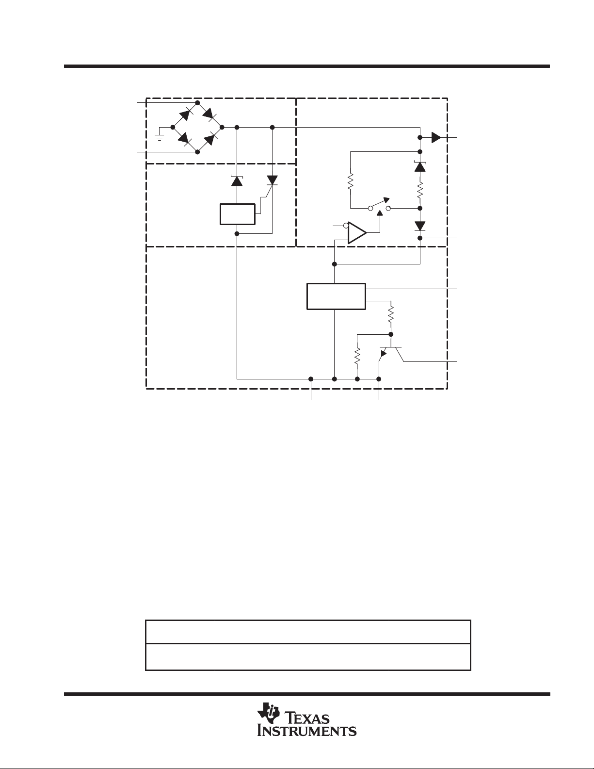
The TCM1520A is a monolithic ring-detection
integrated circuit designed for use in isolated or
nonisolated telephone applications. The device
uses a modified form of the Texas Instruments
BIDFET
CMOS and high-voltage bipolar input/output
circuitry. It features efficient high-voltage (40 V to
150 V) operation with a typical current drain of
1 mA.
During standby, the input impedance is
approximately 1 MΩ or greater, which prevents
any interference with parallel off-hook telephones
transmitting DTMF or voice frequencies. The
device achieves this high input impedance with an
on-chip series zener diode that does not conduct
until the voltage across AC INPUT (pins 1 and 8)
exceeds 8 V . When the voltage across pins 1 and
8 exceeds 18 V , the internal switch is closed, which bypasses the 6.8-V zener diode series resistor . This allows
more efficient power transfer to the load when the device is in the operating mode. In the operating mode, the
impedance of the device varies from 30 kΩ to 7 kΩ over the ring signal of 40 V at 16 Hz to 150 V at 68 Hz and
is reasonably independent of the output load.
†
technology to combine low-voltage
‡
The D package is available taped and reeled with suffix R
added to the device type (i.e., TCM1520ADR).
TCM1520A APPLICATION
Phone Line
TCM1520A
Electronic Telephone
or Accessory
TTL/NMOS/CMOS
Microprocessor
AVAILABLE OPTIONS
T
A
SMALL OUTLINE
TCM1520AD TCM1520AP–40°C to 85°C
AC Ring
Signal
‡
(D)
PACKAGE
PLASTIC DIP
(P)
In typical telephone applications, the TCM1520A is activated through the telephone line by a ring voltage of 40 V
at 16 Hz to 150 V at 68 Hz. The TCM1520A generates a signal suitable to drive an optocoupler or TTL, NMOS,
or CMOS logic. The 5-V OUTPUT can be used as a supply source for optocouplers or low-power logic. This
output is noninverting and is at a high level during ringing.
The TCM1520A incorporates lightning and transient protection that is designed to withstand lightning strikes
of 1.5-kV amplitude and 200-µs duration and also features built-in circuitry to avoid tapping or false triggering
due to transients.
Caution. These devices have limited built-in ESD protection. The leads should be shorted together or the device placed in conductive
foam during storage or handling to prevent electrostatic damage to the MOS gates.
†BIDFET – Bipolar, double-diffused, N-channel and P-channel MOS transistors on same chip. This is a patented process.
PRODUCTION DATA information is current as of publication date.
Products conform to specifications per the terms of Texas Instruments
standard warranty. Production processing does not necessarily include
testing of all parameters.
POST OFFICE BOX 655303 • DALLAS, TEXAS 75265
POST OFFICE BOX 1443
• HOUSTON, TEXAS 77251–1443
Copyright 1990, Texas Instruments Incorporated
1
TCM1520A
DUAL DIFFERENTIAL COMPARATORS
SCTS005B – OCTOBER 1984 – REVISED DECEMBER 1990
functional block diagram
AC INPUT
AC INPUT
1
8
Transient
Protection
Section
Ring-Signal
Voltage Input
Section
45 V 1A
Current
Sensor
Output Section
Regulated
Voltage
V
ref
5-V Series
Regulator
High-Input Impedance/
Antitapping Section
6.8 V
200 Ω
8 kΩ
18 kΩ
5
BELL TAPPING
SENSE
6
C FILTER
4
5-V OUTPUT
2
INVERTING
OUTPUT
37
COMMON COMMON
absolute maximum ratings over operating free-air temperature range (unless otherwise noted)
Continuous supply voltage at C FILTER (see Note 1) 40 V. . . . . . . . . . . . . . . . . . . . . . . . . . . . . . . . . . . . . . . . . .
Continuous differential input voltage, V
Continuous output current at 5-V OUTPUT, I
Continuous SCR on-state input current 200 mA. . . . . . . . . . . . . . . . . . . . . . . . . . . . . . . . . . . . . . . . . . . . . . . . . . . .
SCR on-state input current, I
(duration ≤200 µs) 900 mA. . . . . . . . . . . . . . . . . . . . . . . . . . . . . . . . . . . . . . . . .
I(on)
Continuous total dissipation See Dissipation Rating Table. . . . . . . . . . . . . . . . . . . . . . . . . . . . . . . . . . . . . . . . . . .
Operating free-air temperature range, T
Storage temperature range –40°C to 125°C. . . . . . . . . . . . . . . . . . . . . . . . . . . . . . . . . . . . . . . . . . . . . . . . . . . . . . .
Lead temperature 1,6 mm (1/16 inch) from case for 10 seconds 260°C. . . . . . . . . . . . . . . . . . . . . . . . . . . . . . .
†
Stresses beyond those listed under “absolute maximum ratings” may cause permanent damage to the device. These are stress ratings only, and
functional operation of the device at these or any other conditions beyond those indicated under “recommended operating conditions” is not
implied. Exposure to absolute-maximum-rated conditions for extended periods may affect device reliability.
NOTE 1: All voltage values, unless otherwise noted, are with respect to COMMON (pin 7).
PACKAGE
D 950 mW 7.6 mW/°C 494 mW
P 1000 mW 8.0 mW/°C 520 mW
POWER RATING
(AC INPUT) 40 V. . . . . . . . . . . . . . . . . . . . . . . . . . . . . . . . . . . . . . . . .
ID
DISSIPATION RATING TABLE
TA = 25°C
12 mA. . . . . . . . . . . . . . . . . . . . . . . . . . . . . . . . . . . . . . . . . . . . . . .
O
–40°C to 105°C. . . . . . . . . . . . . . . . . . . . . . . . . . . . . . . . . . . . . . . . . .
A
OPERATING FACTOR
ABOVE TA = 25°C
TA = 85°C
POWER RATING
†
2
POST OFFICE BOX 655303 • DALLAS, TEXAS 75265
POST OFFICE BOX 1443
• HOUSTON, TEXAS 77251–1443
TCM1520A
Impedance when ringing
kΩ
t
Turn-off time
ms
RING DETECTOR
SCTS005B – OCTOBER 1984 – REVISED DECEMBER 1990
recommended operating conditions
MIN MAX UNIT
Input voltage, VIrms (f = 15.3 Hz to 68 Hz) (see Note 2) 40 150 V
Operating free-air temperature, T
NOTE 2: Input voltage is applied to AC INPUT (pins 1 and 8) through a series 2.2-kΩ ± 10% resistor and a 0.47-µF ±10% capacitor. (see
Figures 1, 4, and 5.)
A
electrical characteristics over recommended operating free-air temperature range, RL = open,
C
= 10 µF (unless otherwise noted)
(fltr)
detector section
PARAMETER
V
(BR) CEX
V
OL
V
IT+
V
IT–
V
hys
V
I(on)
V
O
Z
I(off)
I
I(on)
I
I(hold)
†
All characteristics are measured with a 2.2-kΩ resistor and a 0.47-µF capacitor connected at AC INPUT (pin 1) in series with the input signal,
unless otherwise noted.
‡
All typical values are at TA = 25°C.
NOTES: 3. These parameters are measured using pulse techniques (tw ≤ 200 µs, duty cycle ≤ 5%) with C FILTER grounded.
Collector-emitter output breakdown voltage,
INVERTING OUTPUT
Low-level output voltage, INVERTING OUTPUT VID = 25 Vrms, IO = 1.6 mA 1 V
Positive-going input threshold voltage 18 25 V
Negative-going input threshold voltage 6 7 V
Hysteresis (V
Shunt voltage, C FILTER IID = 10 mA 38 50 V
On-state input current, SCR See Note 3 50 100 V
Output voltage, 5-V OUTPUT VID = 40 V, RL = 10 kΩ 4.25 5.75 V
Standby input impedance VIrms = 3 V, f ≤ 20 kHz 1 MΩ
p
On-state input current, SCR (see Note 4)
Input holding current, SCR See Note 3 100 µA
Operating current VID = 40 V, Output open 1 1.6 mA
4. This is the input current required to turn on the SCR.
IT+
– V
) 11 V
IT–
TEST CONDITIONS
VID ≤ 5 Vrms, IO = 5 µA 45 V
VIrms = 40 V, f = 16 Hz 30
VIrms = 130 V, f = 20 Hz 20
See Note 3 55 110 mA
†
MIN
–40 85 °C
‡
TYP
MAX UNIT
switching characteristics at 25°C operating free-air temperature, f = 20 Hz (unless otherwise noted)
t
on
(off)
PARAMETER
Turn-on time VIrms = 40 V 100 ms
POST OFFICE BOX 655303 • DALLAS, TEXAS 75265
POST OFFICE BOX 1443
• HOUSTON, TEXAS 77251–1443
TEST CONDITIONS
VIrms = 40 V 175
VIrms = 60 V to 150 V 300
MIN
TYP
MAX UNIT
3

TCM1520A
RING DETECTOR
SCTS005B – OCTOBER 1984 – REVISED DECEMBER 1990
PARAMETER MEASUREMENT INFORMATION
VIrms = 40 V to 150 V
CAPACITOR VOLTAGE (C FILTER)
DIFFERENTIAL INPUT VOLTAGE
(AC INPUT, PINS 1 AND 8)
18
TA = 25°C
vs
0.47 µF,
350 V
10 µF,
2.2 kΩ
50 V
1
V
ID
8
6
TCM1520A
AC
INPUT
AC
INPUT
C FILTER
COMMON
37
Figure 1. Switching Test Circuit
TYPICAL CHARACTERISTICS
5-V OUTPUT
INVERTING
OUTPUT
OUTPUT VOLTAGE (5-V OUTPUT)
CAPACITOR VOLTAGE (C FILTER)
6
TA = 25°C
4
2
Output
10 kΩ
vs
15
12
9
6
Capacitor Voltage – V
6.8-V Zener Diode
Starts to Conduct
3
0
81012
5
4
Comparator
Switch Fires
14 16 18 20
VID – Differential Input Voltage – V
3
2
– Output Voltage – V
O
V
1
0
45 6
Figure 2 Figure 3
Comparator
Switch Fires
789
Capacitor Voltage – V
10
4
POST OFFICE BOX 655303 • DALLAS, TEXAS 75265
POST OFFICE BOX 1443
• HOUSTON, TEXAS 77251–1443

SCTS005B – OCTOBER 1984 – REVISED DECEMBER 1990
APPLICATION INFORMATION
TCM1520A
RING DETECTOR
VIrms = 40 V to 150 V,
15.3 Hz to 68 Hz
VIrms = 40 V to 150 V,
15.3 Hz to 68 Hz
C1 = 0.47 µF,
350 V
R1 = 2.2 kΩ
C2 = 10 µF,
C1 = 0.47 µF,
350 V
R1 = 2.2 kΩ
TCM1520A
1
50 V
AC
INPUT
V
ID
8
AC
INPUT
6
C FILTER
5-V OUTPUT
COMMON
37
Figure 4. Isolated Configuration
TCM1520A
1
AC
INPUT
V
ID
8
AC
INPUT
6
C FILTER
5-V OUTPUT
INVERTING
OUTPUT
4
4
2
TIL181
To Isolated
Output
R2 = 2.2 kΩ
10 kΩ
Output
C2 = 10 µF,
50 V
COMMON
37
Figure 5. Nonisolated Configuration
NOTE: See Table 1 for component functions.
TABLE 1. COMPONENT FUNCTIONS
COMPONENT
R1 Limits current into SCR during high-voltage transients and aids in dial-pulse rejection.
R2 Limits current into light-emitting diode.
C1
C2 Stores energy from the ring signal to power the 5-V regulator.
Optocoupler Provides ground and transient isolation between the host system and the telephone line.
Blocks dc-battery voltage in standby and aids in filtering dial pulses. Smaller values of C1
improve tapping immunity .
FUNCTION
POST OFFICE BOX 655303 • DALLAS, TEXAS 75265
POST OFFICE BOX 1443
• HOUSTON, TEXAS 77251–1443
5

TCM1520A
RING DETECTOR
SCTS005B – OCTOBER 1984 – REVISED DECEMBER 1990
6
POST OFFICE BOX 655303 • DALLAS, TEXAS 75265
POST OFFICE BOX 1443
• HOUSTON, TEXAS 77251–1443

IMPORTANT NOTICE
T exas Instruments and its subsidiaries (TI) reserve the right to make changes to their products or to discontinue
any product or service without notice, and advise customers to obtain the latest version of relevant information
to verify, before placing orders, that information being relied on is current and complete. All products are sold
subject to the terms and conditions of sale supplied at the time of order acknowledgement, including those
pertaining to warranty, patent infringement, and limitation of liability.
TI warrants performance of its semiconductor products to the specifications applicable at the time of sale in
accordance with TI’s standard warranty. Testing and other quality control techniques are utilized to the extent
TI deems necessary to support this warranty . Specific testing of all parameters of each device is not necessarily
performed, except those mandated by government requirements.
CERT AIN APPLICATIONS USING SEMICONDUCTOR PRODUCTS MAY INVOLVE POTENTIAL RISKS OF
DEATH, PERSONAL INJURY, OR SEVERE PROPERTY OR ENVIRONMENTAL DAMAGE (“CRITICAL
APPLICATIONS”). TI SEMICONDUCTOR PRODUCTS ARE NOT DESIGNED, AUTHORIZED, OR
WARRANTED TO BE SUITABLE FOR USE IN LIFE-SUPPORT DEVICES OR SYSTEMS OR OTHER
CRITICAL APPLICA TIONS. INCLUSION OF TI PRODUCTS IN SUCH APPLICATIONS IS UNDERST OOD TO
BE FULLY AT THE CUSTOMER’S RISK.
In order to minimize risks associated with the customer’s applications, adequate design and operating
safeguards must be provided by the customer to minimize inherent or procedural hazards.
TI assumes no liability for applications assistance or customer product design. TI does not warrant or represent
that any license, either express or implied, is granted under any patent right, copyright, mask work right, or other
intellectual property right of TI covering or relating to any combination, machine, or process in which such
semiconductor products or services might be or are used. TI’s publication of information regarding any third
party’s products or services does not constitute TI’s approval, warranty or endorsement thereof.
Copyright 1998, Texas Instruments Incorporated
 Loading...