

SN54ABT833, SN74ABT833
8-BIT TO 9-BIT PARITY BUS TRANSCEIVERS
SCBS195C – FEBRUARY 1991 – REVISED JANUARY 1997
1
POST OFFICE BOX 655303 • DALLAS, TEXAS 75265
D
State-of-the-Art
EPIC-ΙΙB
BiCMOS Design
Significantly Reduces Power Dissipation
D
ESD Protection Exceeds 2000 V Per
MIL-STD-883, Method 3015; Exceeds 200 V
Using Machine Model (C = 200 pF, R = 0)
D
Latch-Up Performance Exceeds 500 mA Per
JEDEC Standard JESD-17
D
T ypical V
OLP
(Output Ground Bounce) < 1 V
at VCC = 5 V, TA = 25°C
D
High-Drive Outputs (–32-mA IOH,
64-mA IOL)
D
Parity Error Flag With Parity
Generator/Checker
D
Register for Storage of the Parity Error Flag
D
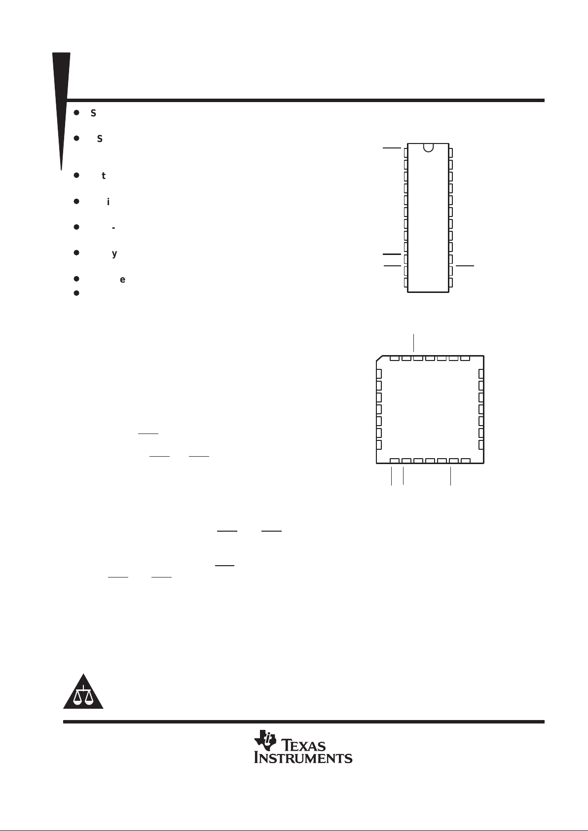
Package Options Include Plastic
Small-Outline (DW) Packages, Ceramic
Chip Carriers (FK), and Plastic (NT) and
Ceramic (JT) DIPs
description
The ’ABT833 8-bit to 9-bit parity transceivers are
designed for communication between data buses.
When data is transmitted from the A bus to the
B bus, a parity bit is generated. When data is
transmitted from the B bus to the A bus with its
corresponding parity bit, the open-collector
parity-error (ERR
) output indicates whether or not
an error in the B data has occurred. The
output-enable (OEA
and OEB) inputs can be used
to disable the device so that the buses are
effectively isolated. The ’ABT833 provide true
data at their outputs.
A 9-bit parity generator/checker generates a
parity-odd (PARITY) output and monitors the
parity of the I/O ports with the ERR flag. ERR is
clocked into the register on the rising edge of the
clock (CLK) input. The error flag register is cleared
with a low pulse on the clear (CLR
) input. When
both OEA and OEB are low, data is transferred
from the A bus to the B bus and inverted parity is
generated. Inverted parity is a forced error
condition that gives the designer more system
diagnostic capability.
Copyright 1997, Texas Instruments Incorporated
UNLESS OTHERWISE NOTED this document contains PRODUCTION
DATA information current as of publication date. Products conform to
specifications per the terms of Texas Instruments standard warranty.
Production processing does not necessarily include testing of all
parameters.
Please be aware that an important notice concerning availability, standard warranty, and use in critical applications of
Texas Instruments semiconductor products and disclaimers thereto appears at the end of this data sheet.
EPIC-ΙΙB is a trademark of Texas Instruments Incorporated.
1
2
3
4
5
6
7
8
9
10
11
12
24
23
22
21
20
19
18
17
16
15
14
13
OEA
A1
A2
A3
A4
A5
A6
A7
A8
ERR
CLR
GND
V
CC
B1
B2
B3
B4
B5
B6
B7
B8
PARITY
OEB
CLK
SN54ABT833 . . . JT PACKAGE
SN74ABT833 ... DW OR NT PACKAGE
(TOP VIEW)
3212827
12 13
5
6
7
8
9
10
11
25
24
23
22
21
20
19
B3
B4
B5
NC
B6
B7
B8
A3
A4
A5
NC
A6
A7
A8
426
14 15 16 1718
ERR
CLR
GND
NC
CLK
OEB
PARITY
A2
A1
OEA
NC
B1
B2
SN54ABT833 . . . FK PACKAGE
(TOP VIEW)
V
CC
NC – No internal connection
SN54ABT833, SN74ABT833
8-BIT TO 9-BIT PARITY BUS TRANSCEIVERS
SCBS195C – FEBRUARY 1991 – REVISED JANUARY 1997
2
POST OFFICE BOX 655303 • DALLAS, TEXAS 75265
description (continued)
T o ensure the high-impedance state during power up or power down, OE should be tied to VCC through a pullup
resistor; the minimum value of the resistor is determined by the current-sinking capability of the driver.
The SN54ABT833 is characterized for operation over the full military temperature range of –55°C to 125°C. The
SN74ABT833 is characterized for operation from –40°C to 85°C.
FUNCTION TABLE
INPUTS
OUTPUT AND I/O
OEB OEA CLR
CLK
Ai
Σ OF H’s
Bi
†
Σ OF H’s
A B PARITY
ERR
‡
FUNCTION
Odd
L
A data to B bus and
LHX
X
Even
NANAAHNA
generate parity
Odd
H
B data to A bus and
HLH↑NA
Even
BNANA
L
check parity
X X L X X X X NA NA H Check error-flag register
H No↑ X NC
LNo↑ X
H
H
H
H ↑ Odd
XZZ
Z
H
Isolati
on
§
H ↑ Even L
Odd
H
A data to B bus and
LLX
X
Even
NANAALNA
generate inverted parity
NA = not applicable, NC = no change, X = don’t care
†
Summation of high-level inputs includes PARITY along with Bi inputs.
‡
Output states shown assume ERR
was previously high.
§
In this mode, ERR
(when clocked) shows inverted parity of the A bus.
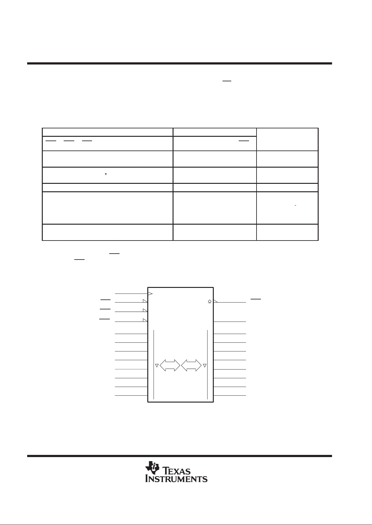
logic symbol
¶
ERR
CLR
OEA
OEB
CLR
11
CLK
13
CLK
1
2
A1
3
A2
4
A3
5
A4
10
PARITY
15
PARITY
B5
19
B6
18
B7
17
B8
16
8
OEA
1
OEB
14
6
A5
7
A6
8
A7
8
9
A8
B1
23
1
B2
22
B3
21
B4
20
ERR
Φ
A Bus B Bus
¶
This symbol is in accordance with ANSI/IEEE Std 91-1984 and IEC Publication 617-12.
Pin numbers shown are for the DW, JT, and NT packages.
SN54ABT833, SN74ABT833
8-BIT TO 9-BIT PARITY BUS TRANSCEIVERS
SCBS195C – FEBRUARY 1991 – REVISED JANUARY 1997
3
POST OFFICE BOX 655303 • DALLAS, TEXAS 75265
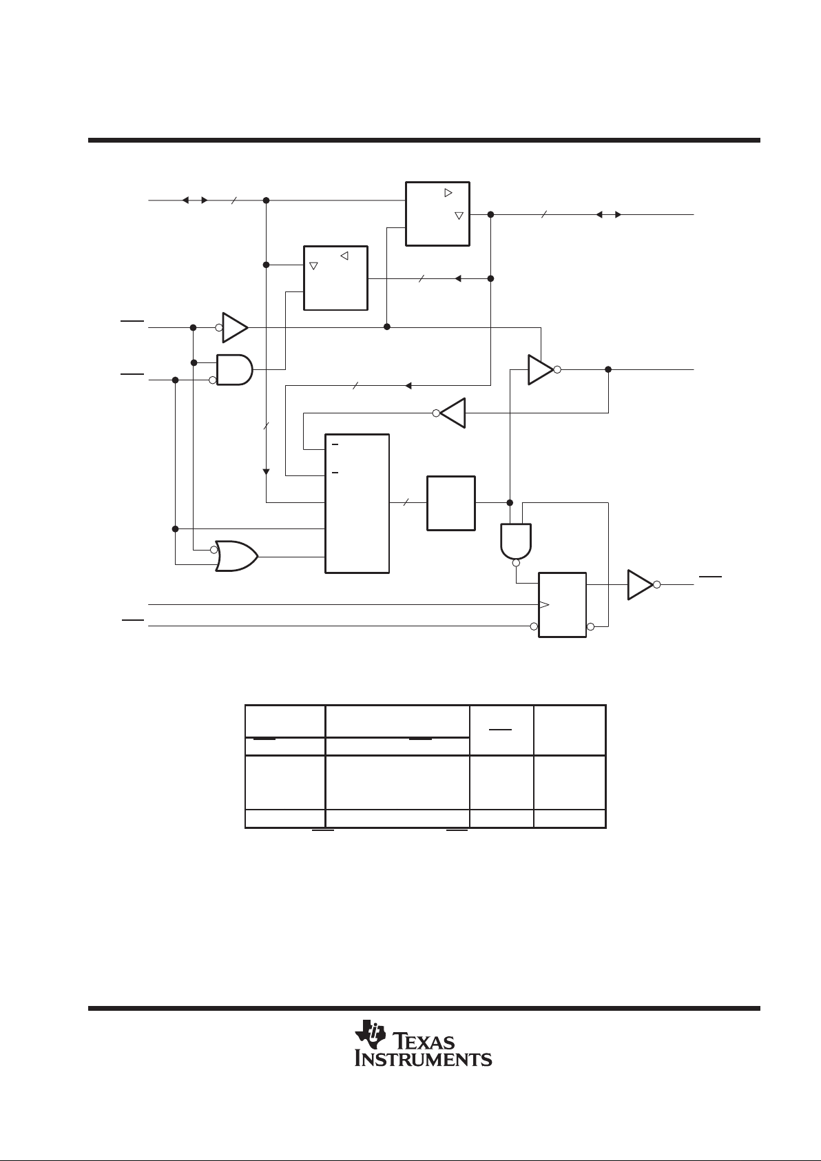
logic diagram (positive logic)
ERR
CLR
OEA
OEB
8
8
8
8
8
9
P
MUX
1
1
1
G1
1
2k
1D
R
C1
EN
EN
8x
8x
A1–A8
CLK
PARITY
B1–B8
15
10
14
1
13
11
2–9
16–23
Pin numbers shown are for the DW, JT, and NT packages.
ERROR-FLAG FUNCTION TABLE
INPUTS
INTERNAL
TO DEVICE
OUTPUT
PRE-STATE
OUTPUT
FUNCTION
CLR CLK POINT P ERR
n–1
†
ERR
H ↑ H H H
H ↑ X LL
Sample
H ↑ L XL
L X X X H Clear
†
The state of ERR before any changes at CLR, CLK, or point P
 Loading...