

Texas Instruments SN65LVDS31-32, SN65LVDS31-32A, SN65LVDS31D, SN65LVDS31DR, SN65LVDS31NS Datasheet
...
SN55LVDS31, SN65LVDS31, SN65LVDS3487, SN65LVDS9638
HIGH-SPEED DIFFERENTIAL LINE DRIVERS
SLLS261F – JULY 1997 – REVISED MARCH 2000
1
POST OFFICE BOX 655303 • DALLAS, TEXAS 75265
D
Meets or Exceeds the Requirements of
ANSI TIA/EIA-644 Standard
D
Low-Voltage Differential Signaling With
Typical Output Voltage of 350 mV and a
100-Ω Load
D
Typical Output Voltage Rise and Fall Times
of 500 ps (400 Mbps)
D
Typical Propagation Delay Times of 1.7 ns
D
Operates From a Single 3.3-V Supply
D
Power Dissipation 25 mW Typical per Driver
at 200 MHz
D
Driver at High Impedance When Disabled or
With VCC = 0
D
Bus-T erminal ESD Protection Exceeds 8 kV
D
Low-Voltage TTL (LVTTL) Logic Input
Levels
D
Pin-Compatible With the AM26LS31,
MC3487, and µA9638
description
The SN55LVDS31, SN65LVDS31,
SN65LVDS3487, and SN65LVDS9638 are
differential line drivers that implement the
electrical characteristics of low-voltage differential
signaling (L VDS). This signaling technique lowers
the output voltage levels of 5 V differential
standard levels (such as TIA/EIA-422B) to reduce
the power, increase the switching speeds, and
allow operation with a 3.3-V supply rail. Any of the
four current-mode drivers will deliver a minimum
differential output voltage magnitude of 247 mV
into a 100-Ω load when enabled.
The intended application of these devices and
signaling technique is for point-to-point baseband
data transmission over controlled impedance
media of approximately 100 Ω. The transmission
media may be printed-circuit board traces,
backplanes, or cables. The ultimate rate and
distance of data transfer is dependent upon the
attenuation characteristics of the media and the
noise coupling to the environment.
The SN65LVDS31, SN65LVDS3487, and
SN65LVDS9638 are characterized for operation
from –40°C to 85°C. The SN55LVDS31 is
characterized for operation from –55°C to 125°C.
Copyright 2000, Texas Instruments Incorporated
PRODUCTION DATA information is current as of publication date.
Products conform to specifications per the terms of Texas Instruments
standard warranty. Production processing does not necessarily include
testing of all parameters.
Please be aware that an important notice concerning availability, standard warranty, and use in critical applications of
Texas Instruments semiconductor products and disclaimers thereto appears at the end of this data sheet.
1
2
3
4
5
6
7
8
16
15
14
13
12
11
10
9
1A
1Y
1Z
G
2Z
2Y
2A
GND
V
CC
4A
4Y
4Z
G
3Z
3Y
3A
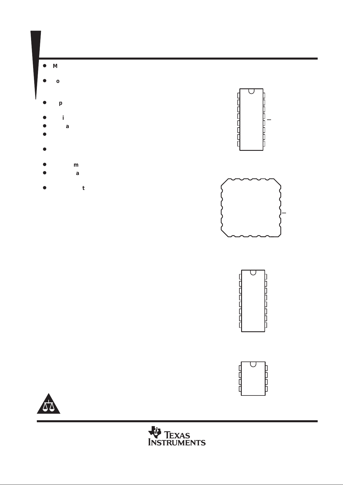
SN55LVDS31 ... J OR W
SN65LVDS31D
(Marked as LVDS31 or 65LVDS31)
(TOP VIEW)
1
2
3
4
5
6
7
8
16
15
14
13
12
11
10
9
1A
1Y
1Z
1,2EN
2Z
2Y
2A
GND
V
CC
4A
4Y
4Z
3,4EN
3Z
3Y
3A
SN65LVDS3487D
(Marked as LVDS3487 or 65LVDS3487)
(TOP VIEW)
1
2
3
4
8
7
6
5
V
CC
1A
2A
GND
1Y
1Z
2Y
2Z
SN65LVDS9638D (Marked as DK638 or LVDS38)
SN65LVDS9638DGN (Marked as L38)
(TOP VIEW)
1920132
17
18
16
15
14
1312119 10
5
4
6
7
8
4Y
4Z
NC
G
3Z
1Z
G
NC
2Z
2Y
1Y1ANCV4A
GND
NC
3A
3Y
2A
SN55LVDS31FK
(TOP VIEW)
CC
SN55LVDS31, SN65LVDS31, SN65LVDS3487, SN65LVDS9638
HIGH-SPEED DIFFERENTIAL LINE DRIVERS
SLLS261F – JULY 1997 – REVISED MARCH 2000
2
POST OFFICE BOX 655303 • DALLAS, TEXAS 75265
AVAILABLE OPTIONS
PACKAGE
T
A
SMALL OUTLINE
(D)
MSOP
(DGN)
CHIP CARRIER
(FK)
CERAMIC DIP
(J)
FLAT PACK
(W)
SN65LVDS31D — — — —
–40°C to 85°C
SN65LVDS3487D — — — —
SN65LVDS9638D SN65LVDS9638DGN — — —
–55°C to 125°C — — SN55LVDS31FK SN55LVDS31J SN55LVDS31W
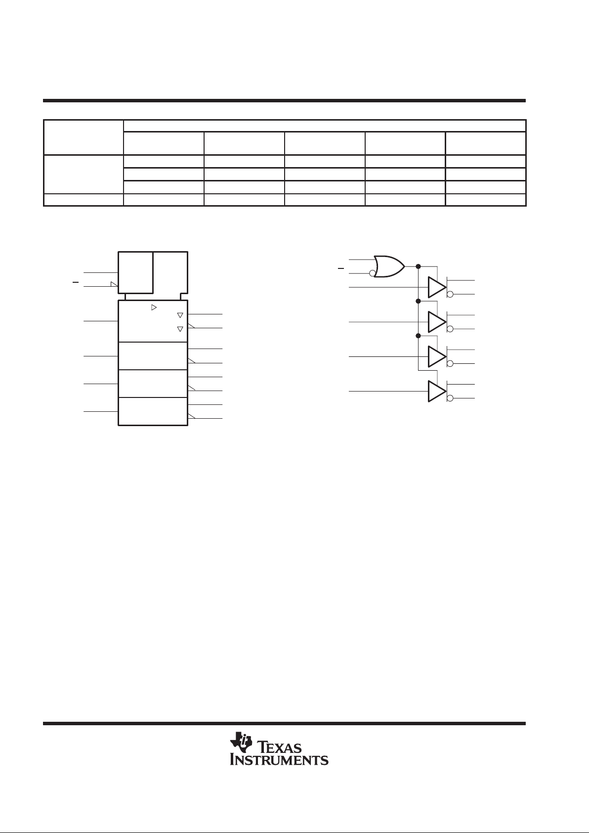
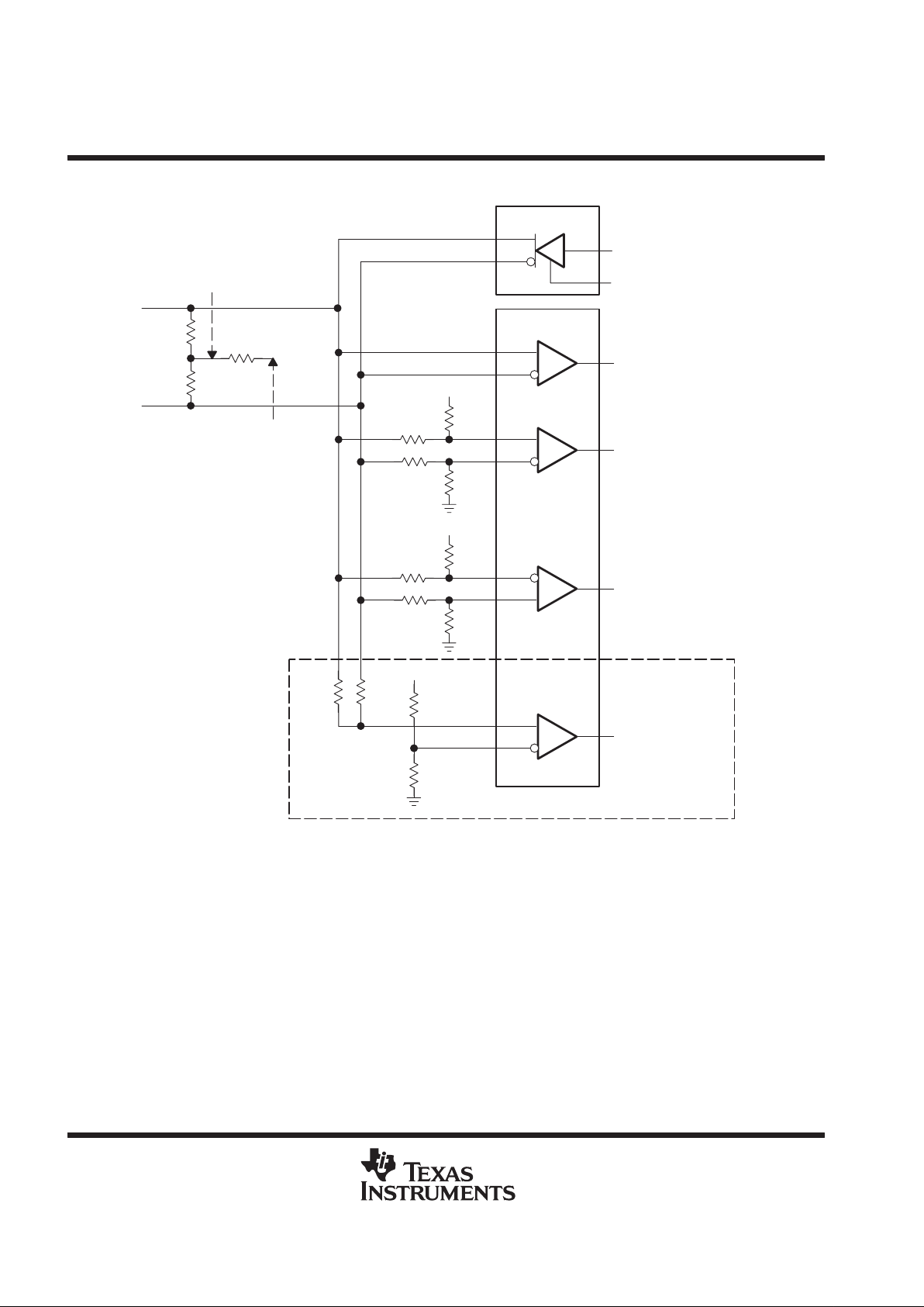
logic symbol
†
SN55LVDS31, SN65LVDS31
4Z
4Y
3Z
3Y
2Z
2Y
1Z
1Y
4A
3A
2A
1A
G
G
13
14
11
10
5
6
3
2
15
9
7
1
12
4
≥ 1
EN
†
This symbol is in accordance with ANSI/IEEE Std 91-1984 and IEC
Publication 617-12.
’LVDS31 logic diagram (positive logic)
4Z
4Y
3Z
3Y
2Z
2Y
1Z
1Y
13
14
11
10
5
6
3
2
4A
3A
2A
1A
G
G
15
9
7
1
12
4
SN55LVDS31, SN65LVDS31, SN65LVDS3487, SN65LVDS9638
HIGH-SPEED DIFFERENTIAL LINE DRIVERS
SLLS261F – JULY 1997 – REVISED MARCH 2000
3
POST OFFICE BOX 655303 • DALLAS, TEXAS 75265
logic symbol
†
EN
EN
4Z
4Y
3Z
3Y
2Z
2Y
1Z
1Y
15
9
12
7
1
4
4A
3A
3,4EN
2A
1A
1,2EN
13
14
11
10
5
6
3
2
SN65LVDS3487
†
This symbol is in accordance with ANSI/IEEE Std 91-1984 and IEC
Publication 617-12.
’LVDS3487 logic diagram (positive logic)
4Z
4Y
3Z
3Y
2Z
2Y
1Z
1Y
13
14
11
10
5
6
3
2
4A
3A
2A
1A
15
9
1
4
7
12
3,4EN
1,2EN
logic symbol
†
2Z
2Y
1Z
1Y
3
2
2A
1A
5
6
7
8
SN65LVDS9638
†
This symbol is in accordance with ANSI/IEEE Std 91-1984 and IEC
Publication 617-12.
’LVDS9638 logic diagram (positive logic)
2Z
2Y
1Z
1Y
5
6
7
8
2A
1A
2
3
SN55LVDS31, SN65LVDS31, SN65LVDS3487, SN65LVDS9638
HIGH-SPEED DIFFERENTIAL LINE DRIVERS
SLLS261F – JULY 1997 – REVISED MARCH 2000
4
POST OFFICE BOX 655303 • DALLAS, TEXAS 75265
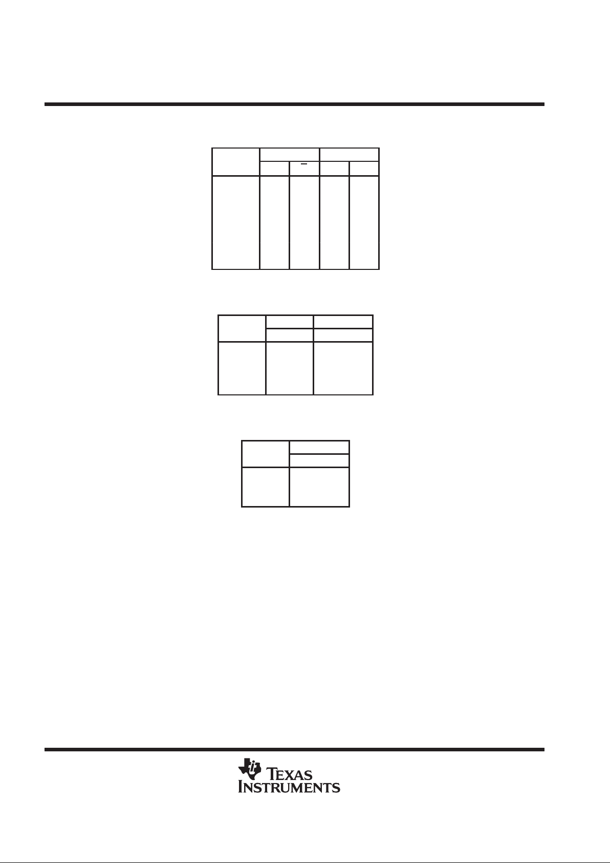
Function Tables
SN55LVDS31, SN65LVDS31
INPUT
ENABLES OUTPUTS
A
G
G
Y Z
H H X H L
L H X L H
H X L H L
L X L L H
X L H Z Z
Open H X L H
Open X L L H
H = high level, L = low level, X = irrelevant,
Z = high impedance (off)
SN65LVDS3487
INPUT
ENABLE OUTPUTS
A
EN Y Z
H H H L
L H L H
X L Z Z
OPEN H L H
H = high level, L = low level, X = irrelevant,
Z = high impedance (off)
SN65LVDS9638
INPUT
OUTPUTS
A
Y Z
H H L
L L H
OPEN L H
H = high level, L = low level
SN55LVDS31, SN65LVDS31, SN65LVDS3487, SN65LVDS9638
HIGH-SPEED DIFFERENTIAL LINE DRIVERS
SLLS261F – JULY 1997 – REVISED MARCH 2000
5
POST OFFICE BOX 655303 • DALLAS, TEXAS 75265
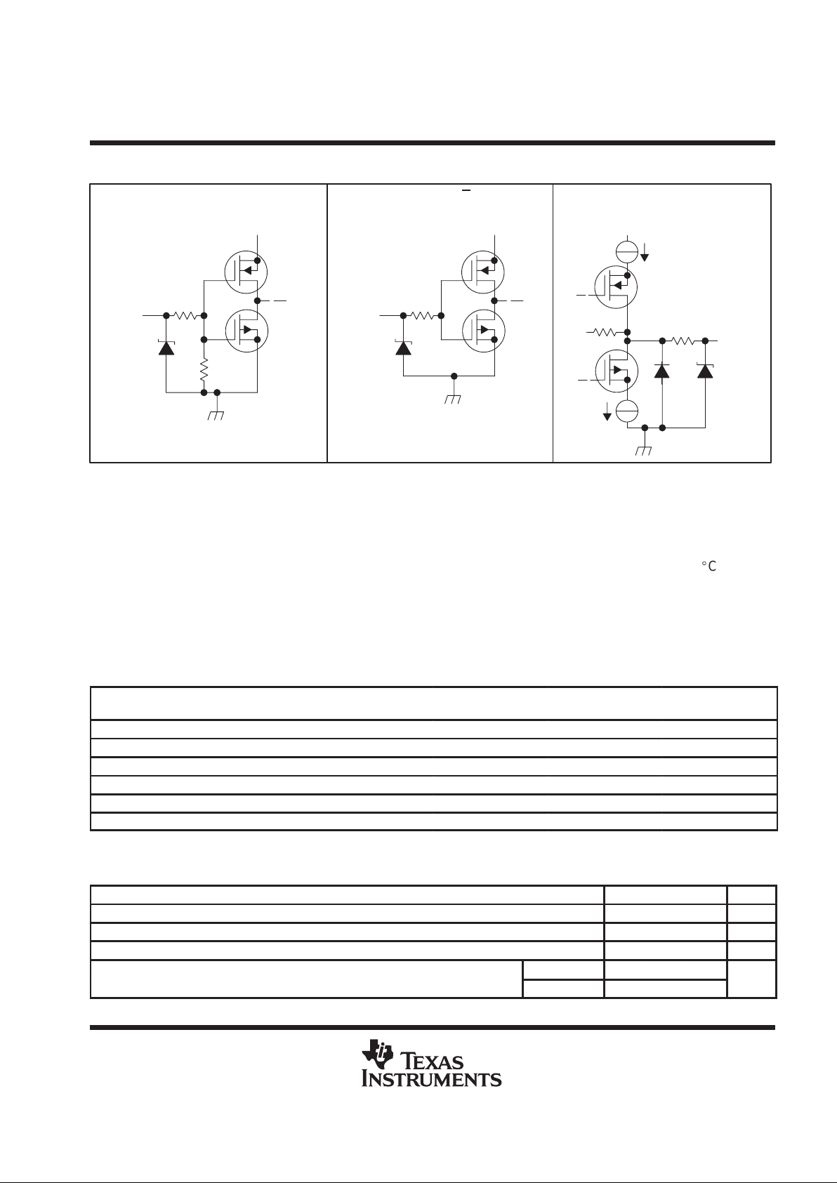
equivalent input and output schematic diagrams
7 V
300 kΩ
50 Ω
V
CC
Input
V
CC
5 Ω
7 V
Y or Z
Output
EQUIVALENT OF EACH A INPUT EQUIVALENT OF G, G, 1,2EN OR
3,4EN INPUTS
TYPICAL OF ALL OUTPUTS
7 V
50 Ω
V
CC
Input
10 kΩ
absolute maximum ratings over operating free-air temperature range (unless otherwise noted)
†
Supply voltage range, VCC (see Note 1) –0.5 V to 4 V. . . . . . . . . . . . . . . . . . . . . . . . . . . . . . . . . . . . . . . . . . . . . . . . . . . .
Input voltage range, V
I
–0.5 V to VCC + 0.5 V. . . . . . . . . . . . . . . . . . . . . . . . . . . . . . . . . . . . . . . . . . . . . . . . . . . . . .
Continuous total power dissipation See Dissipation Rating Table. . . . . . . . . . . . . . . . . . . . . . . . . . . . . . . . . . . . . .
Storage temperature range, T
stg
–65_C to 150°C. . . . . . . . . . . . . . . . . . . . . . . . . . . . . . . . . . . . . . . . . . . . . . . . . . . .
Lead temperature 1,6 mm (1/16 inch) from case for 10 seconds 260°C. . . . . . . . . . . . . . . . . . . . . . . . . . . . . . . .
†
Stresses beyond those listed under “absolute maximum ratings” may cause permanent damage to the device. These are stress ratings only, and
functional operation of the device at these or any other conditions beyond those indicated under “recommended operating conditions” is not
implied. Exposure to absolute-maximum-rated conditions for extended periods may affect device reliability.
NOTE 1: All voltages, except differential I/O bus voltages, are with respect to the network ground terminal.
DISSIPATION RATING T ABLE
PACKAGE
TA ≤ 25°C
POWER RATING
DERATING FACTOR
‡
ABOVE TA = 25°C
TA = 70°C
POWER RATING
TA = 85°C
POWER RATING
TA = 125°C
POWER RATING
D (8) 725 mW 5.8 mW/°C 464 mW 377 mW —
D (16) 950 mW 7.6 mW/°C 608 mW 494 mW —
DGN 2.14 W 17.1 mW/°C 1.37 W 1.11 W —
FK 1375 mW 11.0 mW/°C 880 mW 715 mW 275 mW
J 1375 mW 11.0 mW/°C 880 mW 715 mW 275 mW
W 1000 mW 8.0 mW/°C 640 mW 520 mW 200 mW
‡
This is the inverse of the junction-to-ambient thermal resistance when board-mounted and with no air flow.
recommended operating conditions
MIN NOM MAX UNIT
Supply voltage, V
CC
3 3.3 3.6 V
High-level input voltage, V
IH
2 V
Low-level input voltage, V
IL
0.8 V
p
p
SN65 prefix –40 85
°
Operating free-air temperature, T
A
SN55 prefix –55 125
°C
SN55LVDS31, SN65LVDS31, SN65LVDS3487, SN65LVDS9638
HIGH-SPEED DIFFERENTIAL LINE DRIVERS
SLLS261F – JULY 1997 – REVISED MARCH 2000
6
POST OFFICE BOX 655303 • DALLAS, TEXAS 75265
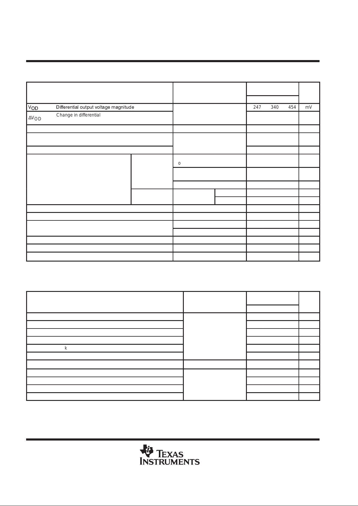
SN65LVDSxxxx electrical characteristics over recommended operating conditions (unless
otherwise noted)
PARAMETER TEST CONDITIONS
SN65LVDS31,
’3487, ’ 9638
UNIT
MIN TYP†MAX
V
OD
Differential output voltage magnitude
247 340 454 mV
∆V
OD
Change in differential output voltage magnitude
between logic states
RL = 100 Ω, See Figure 2
–50
50 mV
V
OC(SS)
Steady-state common-mode output voltage See Figure 3 1.125 1.2 1.375 mV
∆V
OC(SS)
Change in steady-state common-mode output voltage
between logic states
See Figure 3
–50 50 V
V
OC(PP)
Peak-to-peak common-mode output voltage
g
50 150 mV
VI = 0.8 V or 2 V,
No load
Enabled,
9 20 mA
pp
SN65LVDS31,
’3487
VI = 0.8 or 2 V,
Enabled
RL = 100 Ω,
25 35 mA
ICCSu ly current
VI = 0 or VCC,
Disabled
0.25 1 mA
No load
4.7 8 mA
SN65LVDS9638
V
I
= 0.8 V or 2
V
RL = 100 Ω
9 13 mA
I
IH
High-level input current VIH = 2 4 20 µA
I
IL
Low-level input current VIL = 0.8 V 0.1 10 µA
p
V
O(Y)
or V
O(Z)
= 0 –4 –24 mA
IOSShort-circuit output current
VOD = 0 ±12 mA
I
OZ
High-impedance output current VO = 0 or 2.4 V ±1 µA
I
O(OFF)
Power-off output current VCC = 0, VO = 2.4 V ±1 µA
C
I
Input capacitance 3 pF
†
All typical values are at TA = 25°C and with VCC = 3.3 V.
SN65LVDSxxxx switching characteristics over recommended operating conditions (unless
otherwise noted)
PARAMETER TEST CONDITIONS
SN65LVDS31,
’3487, ’ 9638
UNIT
MIN TYP†MAX
t
pLH
Propagation delay time, low-to-high-level output 0.5 1.4 2 ns
t
pHL
Propagation delay time, high-to-low-level output 1 1.7 2.5 ns
t
r
Differential output signal rise time (20% to 80%)
R
= 100 Ω, C
= 10 pF,
0.4 0.5 0.6 ns
t
f
Differential output signal fall time (80% to 20%)
L
,
L
,
See Figure 2
0.4 0.5 0.6 ns
t
sk(p)
Pulse skew (|t
PHL
– t
PLH
|) 0.3 0.6 ns
t
sk(o)
Channel-to-channel output skew
‡
0 0.3 ns
t
sk(pp)
Part-to-part skew
§
800 ps
t
pZH
Propagation delay time, high-impedance-to-high-level output 5.4 15 ns
t
pZL
Propagation delay time, high-impedance-to-low-level output
2.5 15 ns
t
pHZ
Propagation delay time, high-level-to-high-impedance output
See Figure 4
8.1 15 ns
t
pLZ
Propagation delay time, low-level-to-high-impedance output 7.3 15 ns
†
All typical values are at TA = 25°C and with VCC = 3.3 V.
‡
t
sk(o)
is the skew between specified outputs of a single device with all driving inputs connected together and the outputs switching in the same
direction while driving identical specified loads.
§
t
sk(pp)
is the magnitude of the different in propagation delay times between any specified terminals of two devices when both devices operate
with the same supply voltages, same temperature, and have identical packages and test circuits.

SN55LVDS31, SN65LVDS31, SN65LVDS3487, SN65LVDS9638
HIGH-SPEED DIFFERENTIAL LINE DRIVERS
SLLS261F – JULY 1997 – REVISED MARCH 2000
7
POST OFFICE BOX 655303 • DALLAS, TEXAS 75265
SN55LVDS31 electrical characteristics over recommended operating conditions (unless
otherwise noted)
SN55LVDS31
PARAMETER
TEST CONDITIONS
MIN TYP†MAX
UNIT
V
OD
Differential output voltage magnitude
247 340 454 mV
∆V
OD
Change in differential output voltage magnitude
between logic states
RL = 100 Ω, See Figure 2
–50
50 mV
V
OC(SS)
Steady-state common-mode output voltage 1.125 1.2 1.375 V
∆V
OC(SS)
Change in steady-state common-mode output voltage
between logic states
See Figure 3
–50 50 mV
V
OC(PP)
Peak-to-peak common-mode output voltage 50 150 mV
VI = 0.8 V or 2 V,
No load
Enabled,
9 20 mA
I
CC
Supply current
VI = 0.8 or 2 V,
Enabled
RL = 100 Ω,
25 35 mA
VI = 0 or VCC,
Disabled
0.25 1 mA
I
IH
High-level input current VIH = 2 4 20 µA
I
IL
Low-level input current VIL = 0.8 V 0.1 10 µA
p
V
O(Y)
or V
O(Z)
= 0 –4 –24 mA
IOSShort-circuit output current
VOD = 0 ±12 mA
I
OZ
High-impedance output current VO = 0 or 2.4 V ±1 µA
I
O(OFF)
Power-off output current VCC = 0, VO = 2.4 V ±4 µA
C
I
Input capacitance 3 pF
†
All typical values are at TA = 25°C and with VCC = 3.3 V.
SN55LVDS31 switching characteristics over recommended operating conditions (unless
otherwise noted)
SN55LVDS31
PARAMETER
TEST CONDITIONS
MIN TYP†MAX
UNIT
t
pLH
Propagation delay time, low-to-high-level output 0.5 1.4 4 ns
t
pHL
Propagation delay time, high-to-low-level output 1 1.7 4.5 ns
t
r
Differential output signal rise time (20% to 80%)
R
= 100 Ω, C
= 10 pF,
0.4 0.5 1 ns
t
f
Differential output signal fall time (80% to 20%)
L
,
L
,
See Figure 2
0.4 0.5 1 ns
t
sk(p)
Pulse skew (|t
PHL
– t
PLH
|) 0.3 0.6 ns
t
sk(o)
Channel-to-channel output skew
‡
0.3 0.6 ns
t
pZH
Propagation delay time, high-impedance-to-high-level output 5.4 15 ns
t
pZL
Propagation delay time, high-impedance-to-low-level output
2.5 15 ns
t
pHZ
Propagation delay time, high-level-to-high-impedance output
See Figure 4
8.1 17 ns
t
pLZ
Propagation delay time, low-level-to-high-impedance output 7.3 15 ns
†
All typical values are at TA = 25°C and with VCC = 3.3 V.
‡
t
sk(o
) is the maximum delay time difference between drivers on the same device.

SN55LVDS31, SN65LVDS31, SN65LVDS3487, SN65LVDS9638
HIGH-SPEED DIFFERENTIAL LINE DRIVERS
SLLS261F – JULY 1997 – REVISED MARCH 2000
8
POST OFFICE BOX 655303 • DALLAS, TEXAS 75265
PARAMETER MEASUREMENT INFORMATION
V
I
A
(VOY + VOZ)/2
I
OZ
I
OY
Y
Z
V
OD
V
OY
V
OC
I
I
V
OZ
Figure 1. Voltage and Current Definitions
Y
Z
V
OD
Input
(see Note A)
CL = 10 pF
(2 Places)
(see Note B)
100 ± 1 %
2 V
1.4 V
0.8 V
t
PLH
t
PHL
100%
80%
20%
0%
Input
V
OD
0
t
f
t
r
NOTES: A. All input pulses are supplied by a generator having the following characteristics: tr or tf ≤ 1 ns, pulse repetition rate (PRR) = 50 Mpps,
pulse width = 10 ± 0.2 ns.
B. CL includes instrumentation and fixture capacitance within 6 mm of the D.U.T.
Figure 2. Test Circuit, Timing, and Voltage Definitions for the Differential Output Signal
Y
Z
Input
(see Note A)
CL = 10 pF
(2 Places)
(see Note B)
49.9 Ω ± 1% (2 Places)
V
OC
A
A
V
OC
V
OC(PP)
(see Note C)
V
OC(SS)
0
3 V
NOTES: A. All input pulses are supplied by a generator having the following characteristics: tr or tf ≤ 1 ns, pulse repetition rate (PRR) = 50 Mpps,
pulse width = 10 ± 0.2 ns.
B. CL includes instrumentation and fixture capacitance within 6 mm of the D.U.T.
C. The measurement of V
OC(PP)
is made on test equipment with a –3 dB bandwidth of at least 300 MHz.
Figure 3. Test Circuit and Definitions for the Driver Common-Mode Output Voltage

SN55LVDS31, SN65LVDS31, SN65LVDS3487, SN65LVDS9638
HIGH-SPEED DIFFERENTIAL LINE DRIVERS
SLLS261F – JULY 1997 – REVISED MARCH 2000
9
POST OFFICE BOX 655303 • DALLAS, TEXAS 75265
PARAMETER MEASUREMENT INFORMATION
Y
Z
Inputs
(see Note A)
CL = 10 pF
(2 Places)
(see Note B)
49.9 Ω ± 1% (2 Places)
G
G
1.2 V
t
PZH
t
PHZ
t
PZL
t
PLZ
2 V
1.4 V
0.8 V
100%, ≅ 1.4 V
1.4 V
2 V
0.8 V
50%
0%, 1.2 V
0%, ≅ 1 V
100%, 1.2 V
50%
G, 1,2EN,
OR 3,4EN
G
V
OY
or
V
OZ
V
OZ
or
V
OY
A at 2 V, G
at VCC and Input to G
or
G at GND and Input to G
for ’LVDS31 only
A at 0.8 V, G
at VCC and Input to G
or
G at GND and Input to G
for ’LVDS31 only
V
OYVOZ
0.8 V or 2 V
1,2EN or 3,4EN
NOTES: A. All input pulses are supplied by a generator having the following characteristics: tr or tf < 1 ns, pulse repetition rate (PRR) = 0.5 Mpps,
pulse width = 500 ± 10 ns.
B. CL includes instrumentation and fixture capacitance within 6 mm of the D.U.T.
Figure 4. Enable and Disable Time Circuit and Definitions

SN55LVDS31, SN65LVDS31, SN65LVDS3487, SN65LVDS9638
HIGH-SPEED DIFFERENTIAL LINE DRIVERS
SLLS261F – JULY 1997 – REVISED MARCH 2000
10
POST OFFICE BOX 655303 • DALLAS, TEXAS 75265
TYPICAL CHARACTERISTICS
Figure 5
Four Drivers Loaded Per
Figure 3 and Switching
Simultaneously.
29
27
19
15
50 100
– Supply Current – mA
31
33
f – Frequency – MHz
SN55LVDS31, SN65LVDS31
SUPPLY CURRENT
vs
FREQUENCY
35
150 200
21
VCC = 3.6 V
I
CC
VCC = 3.3 V
25
23
17
VCC = 3 V
Figure 6
1.5
1.4
1.2
1
1.7
1.9
–40 –20 0
LOW-TO-HIGH PROPAGATION DELAY TIME
vs
FREE-AIR TEMPERATURE
20 40
TA – Free-Air Temperature – °C
VCC = 3 V
VCC = 3.6 V
1.8
1.6
1.3
1.1
60 80 100
VCC = 3.3 V
– Low-To-High Propagation Delay T ime – ns
t
PLH
Figure 7
HIGH-TO-LOW PROPAGATION DELAY TIME
vs
FREE-AIR TEMPERATURE
1.5
1.4
1.2
1
1.7
1.9
–40 –20 0 20 40
TA – Free-Air Temperature – °C
VCC = 3 V
1.8
1.6
1.3
1.1
60 80 100
VCC = 3.3 V
VCC = 3.6 V
t
PHL
– High-To-Low Propagation Delay T ime – ns

SN55LVDS31, SN65LVDS31, SN65LVDS3487, SN65LVDS9638
HIGH-SPEED DIFFERENTIAL LINE DRIVERS
SLLS261F – JULY 1997 – REVISED MARCH 2000
11
POST OFFICE BOX 655303 • DALLAS, TEXAS 75265
APPLICATIONS INFORMATION
The devices are generally used as building blocks for high-speed point-to-point data transmission where ground
differences are less than 1 V . Devices can interoperate with RS-422, PECL, and IEEE-P1596. Drivers/receivers
approach ECL speeds without the power and dual supply requirements.
10
1
0.1
Transmission Distance – m
100
Signaling Rate – Mbps
TRANSMISSION DISTANCE
vs
SIGNALING RATE
10 100 1000
5% Jitter
(see Note A)
30% Jitter
(see Note A)
24 AWG UTP 96 Ω
(PVC Dielectric)
NOTE A: This parameter is the percentage of distortion of the unit interval (UI) with a pseudo-random data pattern.
Figure 8. T ypical Transmission Distance Versus Signaling Rate
1A
1Y
1Z
G
2Z
2Y
2A
GND
V
CC
4A
4Y
4Z
G
3Z
3Y
3A
1
2
3
4
5
6
7
8
16
15
14
13
12
11
10
9
ZO = 100 Ω
ZO = 100 Ω
ZO = 100 Ω
ZO = 100 Ω
3.3 V
0.1 µF
(see Note A)
0.001 µF
(see Note A)
V
CC
See Note B
NOTES: A. Place a 0.1 µF and a 0.001 µF Z5U ceramic, mica or polystyrene dielectric, 0805 size, chip capacitor between VCC and the ground
plane. The capacitors should be located as close as possible to the device terminals.
B. Unused enable inputs should be tied to VCC or GND as appropriate.
Figure 9. Typical Application Circuit Schematic
SN55LVDS31, SN65LVDS31, SN65LVDS3487, SN65LVDS9638
HIGH-SPEED DIFFERENTIAL LINE DRIVERS
SLLS261F – JULY 1997 – REVISED MARCH 2000
12
POST OFFICE BOX 655303 • DALLAS, TEXAS 75265
APPLICATIONS INFORMATION
1/4 ’LVDS31
’LVDS32
500 Ω
500 Ω
20 kΩ
20 kΩ
3.3 V
500 Ω
500 Ω
20 kΩ
20 kΩ
3.3 V
7 kΩ7 kΩ
10 kΩ
3.3 kΩ
Twisted-Pair B Only
Strb/Data_TX
Strb/Data_Enable
Data/Strobe
1 Arb_RX
2 Arb_RX
Port_Status
TpBias on
Twisted-Pair A
55 Ω
55 Ω
5 kΩ
VG on
Twisted-Pair B
TP
TP
3.3 V
NOTES: A. Resistors are leadless thick-film (0603) 5% tolerance.
B. Decoupling capacitance is not shown but recommended.
C. VCC is 3 V to 3.6 V.
D. The differential output voltage of the ’LVDS31 can exceed that specified by IEEE1394.
Figure 10. 100 Mbps IEEE1394 Transceiver

SN55LVDS31, SN65LVDS31, SN65LVDS3487, SN65LVDS9638
HIGH-SPEED DIFFERENTIAL LINE DRIVERS
SLLS261F – JULY 1997 – REVISED MARCH 2000
13
POST OFFICE BOX 655303 • DALLAS, TEXAS 75265
APPLICATIONS INFORMATION
1A
1Y
1Z
G
2Z
2Y
2A
GND
V
CC
4A
4Y
4Z
G
3Z
3Y
3A
1
2
3
4
5
6
7
8
16
15
14
13
12
11
10
9
ZO = 100 Ω
ZO = 100 Ω
ZO = 100 Ω
ZO = 100 Ω
≈3.6 V
0.1 µF
(see Note A)
V
CC
See Note B
1N645
(2 places)
0.01 µF
5 V
NOTE A: Place a 0.1 µF Z5U ceramic, mica or polystyrene dielectric, 0805 size, chip capacitor between VCC and the ground plane. The capacitor
should be located as close as possible to the device terminals.
Figure 11. Operation with a 5-V Supply
related information
IBIS modeling is available for this device. Please contact the local TI sales office or the TI Web site at
www.ti.com
for more information.
For more application guidelines, please see the following documents:
D
Low-Voltage Differential Signalling Design Notes
(TI literature number SLLA014)
D
Interface Circuits for TIA/EIA-644
(LVDS) (SLLA038)
D
Reducing EMI with LVDS
(SLLA030)
D
Slew Rate Control of LVDS Circuits
(SLLA034)
D
Using an LVDS Receiver with RS-422 Data
(SLLA031)
D
Evaluating the LVDS EVM
(SLLA033)

SN55LVDS31, SN65LVDS31, SN65LVDS3487, SN65LVDS9638
HIGH-SPEED DIFFERENTIAL LINE DRIVERS
SLLS261F – JULY 1997 – REVISED MARCH 2000
14
POST OFFICE BOX 655303 • DALLAS, TEXAS 75265
MECHANICAL INFORMATION
D (R-PDSO-G**) PLASTIC SMALL-OUTLINE PACKAGE
14 PIN SHOWN
4040047/D 10/96
0.228 (5,80)
0.244 (6,20)
0.069 (1,75) MAX
0.010 (0,25)
0.004 (0,10)
1
14
0.014 (0,35)
0.020 (0,51)
A
0.157 (4,00)
0.150 (3,81)
7
8
0.044 (1,12)
0.016 (0,40)
Seating Plane
0.010 (0,25)
PINS **
0.008 (0,20) NOM
A MIN
A MAX
DIM
Gage Plane
0.189
(4,80)
(5,00)
0.197
8
(8,55)
(8,75)
0.337
14
0.344
(9,80)
16
0.394
(10,00)
0.386
0.004 (0,10)
M
0.010 (0,25)
0.050 (1,27)
0°–8°
NOTES: A. All linear dimensions are in inches (millimeters).
B. This drawing is subject to change without notice.
C. Body dimensions do not include mold flash or protrusion, not to exceed 0.006 (0,15).
D. Falls within JEDEC MS-012

SN55LVDS31, SN65LVDS31, SN65LVDS3487, SN65LVDS9638
HIGH-SPEED DIFFERENTIAL LINE DRIVERS
SLLS261F – JULY 1997 – REVISED MARCH 2000
15
POST OFFICE BOX 655303 • DALLAS, TEXAS 75265
MECHANICAL INFORMATION
DGN (S-PDSO-G8) PowerPAD PLASTIC SMALL-OUTLINE PACKAGE
0,69
0,41
0,25
Thermal Pad
(See Note D)
0,15 NOM
Gage Plane
4073271/A 01/98
4,98
0,25
5
3,05
4,78
2,95
8
4
3,05
2,95
1
0,38
0,15
0,05
1,07 MAX
Seating Plane
0,10
0,65
M
0,25
0°–6°
NOTES: A. All linear dimensions are in millimeters.
B. This drawing is subject to change without notice.
C. Body dimensions include mold flash or protrusions.
D. The package thermal performance may be enhanced by attaching an external heat sink to the thermal pad. This pad is electrically
and thermally connected to the backside of the die and possibly selected leads.
E. Falls within JEDEC MO-187
PowerPAD is a trademark of Texas Instruments Incorporated.

SN55LVDS31, SN65LVDS31, SN65LVDS3487, SN65LVDS9638
HIGH-SPEED DIFFERENTIAL LINE DRIVERS
SLLS261F – JULY 1997 – REVISED MARCH 2000
16
POST OFFICE BOX 655303 • DALLAS, TEXAS 75265
MECHANICAL INFORMATION
FK (S-CQCC-N**) LEADLESS CERAMIC CHIP CARRIER
4040140/D 10/96
28 TERMINAL SHOWN
B
0.358
(9,09)
MAX
(11,63)
0.560
(14,22)
0.560
0.458
0.858
(21,8)
1.063
(27,0)
(14,22)
A
NO. OF
MINMAX
0.358
0.660
0.761
0.458
0.342
(8,69)
MIN
(11,23)
(16,26)
0.640
0.739
0.442
(9,09)
(11,63)
(16,76)
0.962
1.165
(23,83)
0.938
(28,99)
1.141
(24,43)
(29,59)
(19,32)(18,78)
**
20
28
52
44
68
84
0.020 (0,51)
TERMINALS
0.080 (2,03)
0.064 (1,63)
(7,80)
0.307
(10,31)
0.406
(12,58)
0.495
(12,58)
0.495
(21,6)
0.850
(26,6)
1.047
0.045 (1,14)
0.045 (1,14)
0.035 (0,89)
0.035 (0,89)
0.010 (0,25)
12
1314151618 17
11
10
8
9
7
5
432
0.020 (0,51)
0.010 (0,25)
6
12826 27
19
21
B SQ
A SQ
22
23
24
25
20
0.055 (1,40)
0.045 (1,14)
0.028 (0,71)
0.022 (0,54)
0.050 (1,27)
NOTES: A. All linear dimensions are in inches (millimeters).
B. This drawing is subject to change without notice.
C. This package can be hermetically sealed with a metal lid.
D. The terminals are gold plated.
E. Falls within JEDEC MS-004

SN55LVDS31, SN65LVDS31, SN65LVDS3487, SN65LVDS9638
HIGH-SPEED DIFFERENTIAL LINE DRIVERS
SLLS261F – JULY 1997 – REVISED MARCH 2000
17
POST OFFICE BOX 655303 • DALLAS, TEXAS 75265
MECHANICAL INFORMATION
J (R-GDIP-T**) CERAMIC DUAL-IN-LINE PACKAGE
1
20
0.290
(7,87)
0.310
0.975
(24,77)
(23,62)
0.930
(7,37)
0.245
(6,22)
(7,62)
0.300
181614
PINS **
0.290
(7,87)
0.310
0.785
(19,94)
(19,18)
0.755
(7,37)
0.310
(7,87)
(7,37)
0.290
0.755
(19,18)
(19,94)
0.785
0.245
(6,22)
(7,62)
0.300A0.300
(7,62)
(6,22)
0.245
A MIN
A MAX
B MAX
B MIN
C MIN
C MAX
DIM
0.310
(7,87)
(7,37)
0.290
(23,10)
0.910
0.300
(7,62)
(6,22)
0.245
0°–15°
Seating Plane
0.014 (0,36)
0.008 (0,20)
4040083/D 08/98
C
8
7
0.020 (0,51) MIN
B
0.070 (1,78)
0.100 (2,54)
0.065 (1,65)
0.045 (1,14)
14 PIN SHOWN
14
0.015 (0,38)
0.023 (0,58)
0.100 (2,54)
0.200 (5,08) MAX
0.130 (3,30) MIN
NOTES: A. All linear dimensions are in inches (millimeters).
B. This drawing is subject to change without notice.
C. This package can be hermetically sealed with a ceramic lid using glass frit.
D. Index point is provided on cap for terminal identification only on press ceramic glass frit seal only.
E. Falls within MIL STD 1835 GDIP1-T14, GDIP1-T16, GDIP1-T18, GDIP1-T20, and GDIP1-T22.

SN55LVDS31, SN65LVDS31, SN65LVDS3487, SN65LVDS9638
HIGH-SPEED DIFFERENTIAL LINE DRIVERS
SLLS261F – JULY 1997 – REVISED MARCH 2000
18
POST OFFICE BOX 655303 • DALLAS, TEXAS 75265
MECHANICAL INFORMATION
W (R-GDFP-F16) CERAMIC DUAL FLATPACK
0.235 (5,97)
0.355 (9,02) 0.355 (9,02)
0.235 (5,97)
98
161
0.745 (18,92)
0.245 (6,22)
0.004 (0,10)
0.026 (0,66)
0.015 (0,38)
0.015 (0,38)
0.045 (1,14)
0.371 (9,42)
0.006 (0,15)
0.045 (1,14)
Base and Seating Plane
0.025 (0,64)
0.019 (0,48)
0.440 (11,18)
0.285 (7,24)
0.085 (2,16)
1.025 (26,04)
4040180-3/B 03/95
0.275 (6,99)
0.305 (7,75)
0.050 (1,27)
NOTES: A. All linear dimensions are in inches (millimeters).
B. This drawing is subject to change without notice.
C. This package can be hermetically sealed with a ceramic lid using glass frit.
D. Index point is provided on cap for terminal identification only.
E. Falls within MIL-STD-1835 GDFP1-F16 and JEDEC MO-092AC

IMPORTANT NOTICE
T exas Instruments and its subsidiaries (TI) reserve the right to make changes to their products or to discontinue
any product or service without notice, and advise customers to obtain the latest version of relevant information
to verify, before placing orders, that information being relied on is current and complete. All products are sold
subject to the terms and conditions of sale supplied at the time of order acknowledgement, including those
pertaining to warranty, patent infringement, and limitation of liability.
TI warrants performance of its semiconductor products to the specifications applicable at the time of sale in
accordance with TI’s standard warranty. Testing and other quality control techniques are utilized to the extent
TI deems necessary to support this warranty. Specific testing of all parameters of each device is not necessarily
performed, except those mandated by government requirements.
CERT AIN APPLICATIONS USING SEMICONDUCTOR PRODUCTS MAY INVOLVE POTENTIAL RISKS OF
DEATH, PERSONAL INJURY, OR SEVERE PROPERTY OR ENVIRONMENTAL DAMAGE (“CRITICAL
APPLICATIONS”). TI SEMICONDUCTOR PRODUCTS ARE NOT DESIGNED, AUTHORIZED, OR
WARRANTED TO BE SUITABLE FOR USE IN LIFE-SUPPORT DEVICES OR SYSTEMS OR OTHER
CRITICAL APPLICATIONS. INCLUSION OF TI PRODUCTS IN SUCH APPLICA TIONS IS UNDERSTOOD T O
BE FULLY AT THE CUSTOMER’S RISK.
In order to minimize risks associated with the customer’s applications, adequate design and operating
safeguards must be provided by the customer to minimize inherent or procedural hazards.
TI assumes no liability for applications assistance or customer product design. TI does not warrant or represent
that any license, either express or implied, is granted under any patent right, copyright, mask work right, or other
intellectual property right of TI covering or relating to any combination, machine, or process in which such
semiconductor products or services might be or are used. TI’s publication of information regarding any third
party’s products or services does not constitute TI’s approval, warranty or endorsement thereof.
Copyright 2000, Texas Instruments Incorporated
 Loading...