

www.ti.com
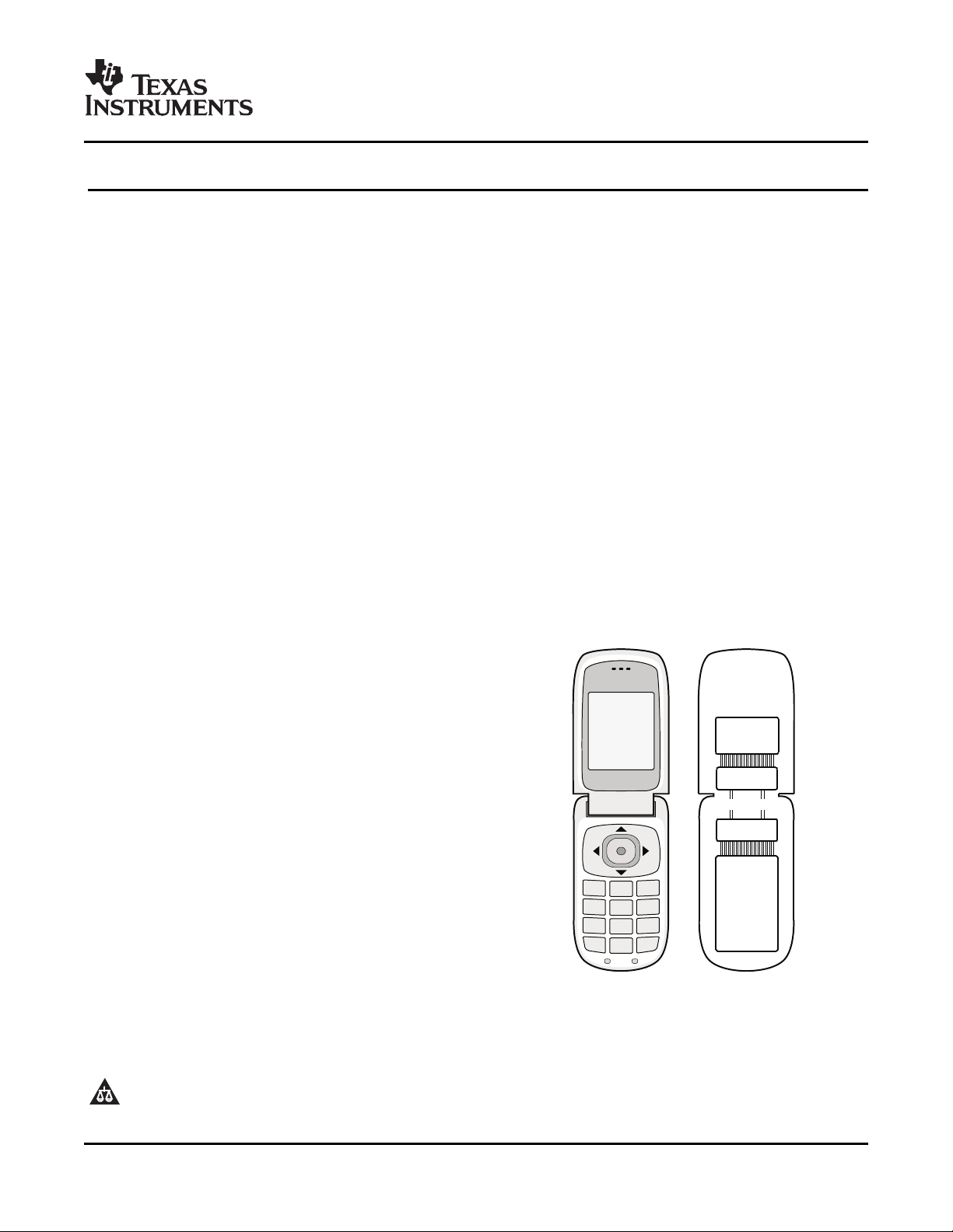
Flatlink 3Gä
1
4
7
*
3
6
9
#
2
5
8
0
Application
Processor
with
RGB
Video
Interface
LVDS306
LVDS305
LCD
Driver
DATACLK
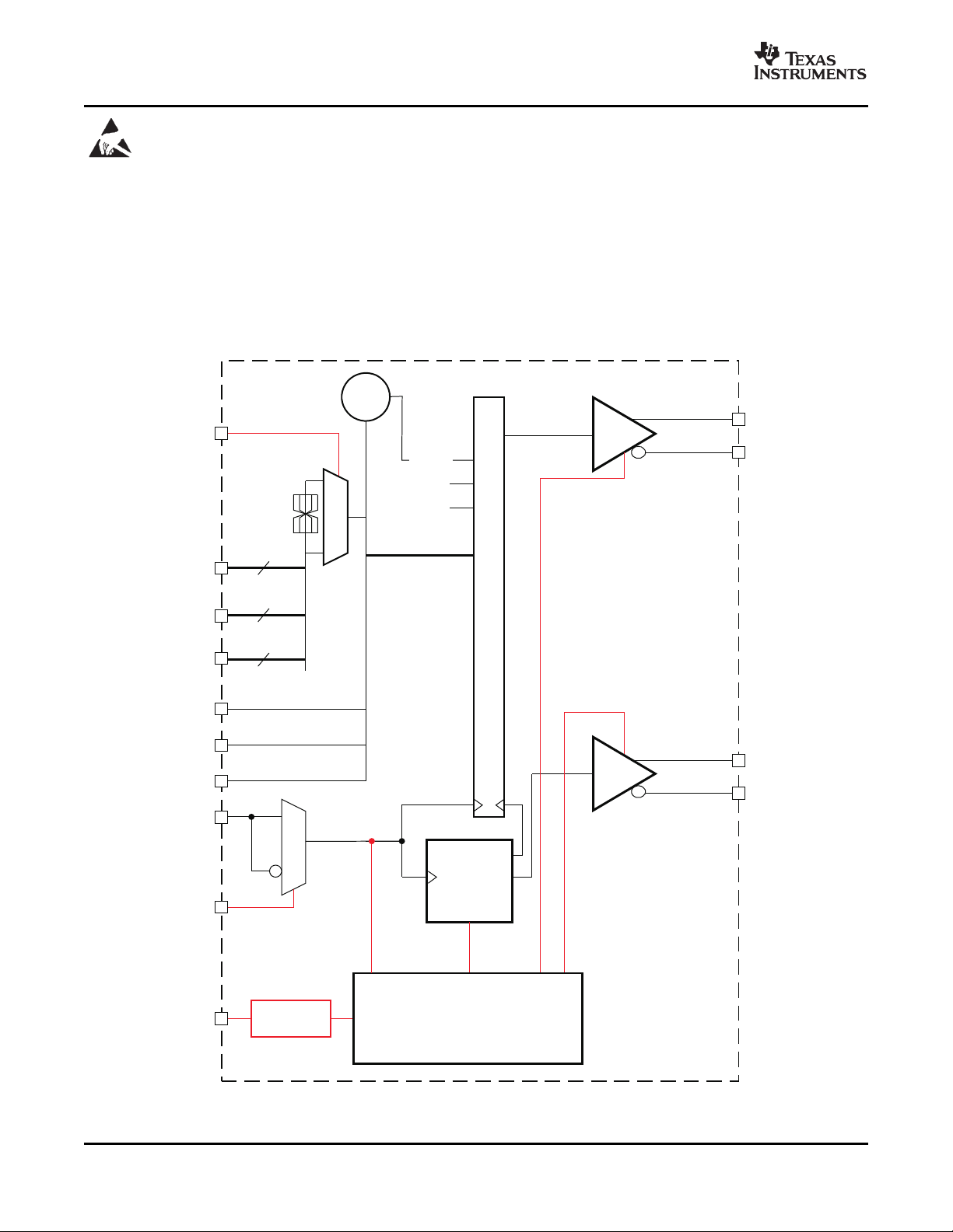
PROGRAMMABLE 27-BIT DISPLAY SERIAL INTERFACE TRANSMITTER
SN65LVDS305
SLLS744A – AUGUST 2006 – REVISED JANUARY 2007
FEATURES
• FlatLink™3G Serial-Interface Technology
• Compatible With FlatLink3G Receivers Such
as SN65LVDS306
• Input Supports 24-bit RGB Video Mode
Interface
• 24-Bit RGB Data, 3 Control Bits, 1 Parity Bit,
and 2 Reserved Bits Transmitted Over One
Differential Line
• SubLVDS Differential Voltage Levels
• Effective Data Throughput up to 405 Mbps
• Three Operating Modes to Conserve Power
– Active-Mode QVGA 17.4 mW (Typical)
– Shutdown Mode ≈ 0.5 µ A (Typical)
– Standby Mode ≈ 0.5 µ A (Typical)
• Bus Swap for Increased PCB Layout
Flexibility
• 1.8-V Supply Voltage
• ESD Rating > 2 kV (HBM)
• Typical Application: Host-Controller to
Display-Module Interface
• Pixel Clock Range of 4 MHz–15 MHz
• Failsafe on all CMOS Inputs
• Packaging: 80-Terminal 5-mm × 5-mm µ BGA
FPC cabling typically interconnects the
SN65LVDS305 with the display. Compared to
parallel signaling, the SN65LVDS305 outputs reduce
the EMI of the interconnect by over 20 dB.
The SN65LVDS305 supports three power modes
(shutdown, standby and active) to conserve power.
When transmitting, the PLL locks to the incoming
pixel clock, PCLK, and generates an internal
high-speed clock at the line rate of the data lines.
The parallel data are latched on the rising or falling
edge of PCLK, as selected by the external control
signal CPOL. The serialized data is presented on the
serial output, D, together with a recreated PCLK
generated from the internal high-speed clock that is
output on CLK. If PCLK stops, the device enters a
standby mode to conserve power.
The parallel (CMOS) input bus offers a bus-swap
feature. The SWAP terminal configures the input
order of the pixel data to be either R[7:0]. G[7:0],
B[7:0], VS, HS, DE or B[0:7]. G[0:7], R[0:7], VS, HS,
DE. This gives a PCB designer the flexibility to better
match the bus to the host controller pinout or to put
the transmitter device on the top side or the bottom
side of the PCB.
®
DESCRIPTION
The SN65LVDS305 serializer device converts 27
parallel data inputs to one sub-low-voltage
differential signaling (SubLVDS) serial output. It
loads a shift register with 24 pixel bits and 3 control
bits from the parallel CMOS input interface. In
addition to the 27 data bits, the device adds a parity
bit and two reserved bits into a 30-bit data word.
Each word is latched into the device by the pixel
clock (PCLK). The parity bit (odd parity) allows a
receiver to detect single bit errors. The serial shift
register is uploaded at 30 times the pixel-clock data
rate. A copy of the pixel clock is output on a separate
differential output.
FlatLink is a trademark of Texas Instruments.
µ BGA is a registered trademark of Tessera, Inc..
PRODUCTION DATA information is current as of publication date.
Products conform to specifications per the terms of the Texas
Instruments standard warranty. Production processing does not
necessarily include testing of all parameters.
Please be aware that an important notice concerning availability, standard warranty, and use in critical applications of Texas
Instruments semiconductor products and disclaimers thereto appears at the end of this data sheet.
Copyright © 2006–2007, Texas Instruments Incorporated
www.ti.com
[0..26]
0
1
TXEN
PCLK
VS
HS
B[0:7]
G[0:7]
R[0:7]
DE
8
8
8
D+
D–
SubLVDS
SubLVDS
CLK+
CLK–
CPOL
SWAP
1
0
iPCLK
Bit28=0
Bit27=0
Bit29
Glitch
Supression
Control/StandbyMonitor
Parity
Calc
1 30-BitParallel-to-SerialConversion´
´10
´1
PLL
Multiplier
SN65LVDS305
SLLS744A – AUGUST 2006 – REVISED JANUARY 2007
These devices have limited built-in ESD protection. The leads should be shorted together or the device placed in conductive foam
during storage or handling to prevent electrostatic damage to the MOS gates.
DESCRIPTION (CONTINUED)
The TXEN input can be used to put the SN65LVDS305 in a shutdown mode. The SN65LVDS305 enters an
active standby mode if the input clock, PCLK, stops. This minimizes power consumption without the need for
controlling an external terminal. The SN65LVDS305 is characterized for operation over ambient air temperatures
of –40 ° C to 85 ° C. All CMOS inputs offer failsafe to protect the input from damage during power up and to avoid
current flow into the device inputs during power up. An input voltage of up to 2.165 V can be applied to all
CMOS inputs while V
is between 0 V and 1.65 V.
DD
Functional Block Diagram
2
Submit Documentation Feedback
www.ti.com
PINOUT – TOP VIEW
9
8764 5321
A
D
C
B
G
F
E
H
J
D–
G0
/G7
B7/R0
NC
NC
NC
NC
D+ CLK+
CLK–
R7/B0
V
DDLVDS
GND
LVDS
V
DDPLLD
GND
PLLD
GND
PLLA
VDD
B0/R7
GND
LVDS
GND
GND
VDD
DE
GND
GND
GND
HS VS
GND
GND
GND
GNDPCLK
TXEN
VDD
V
DDPLLA
GND
B5
/R2 VDD
B1
/R6
VDD
GND
B4
/R3
VDDB2/R5
B3/R4
GND
GND
GND GND
GND
GND
GND
GND
GND
GND
GND
B6
/R1
SWAP
GND
GND
CPOL
GND
VDD
V
DDLVDS
R1/B6
G6/G1
G5/G2G3/G4
G2/G5
G1/G6 R3/B4
R6/B1
R5/B2
R2/B5 R4/B3
G7/G0
R0/B7G4/G3
GND
LVDS
RGBInputpinassignmentbasedonSWAP pinsetting:
SWAP=0/SWAP=1
SN65LVDS305
SLLS744A – AUGUST 2006 – REVISED JANUARY 2007
Submit Documentation Feedback
3
www.ti.com
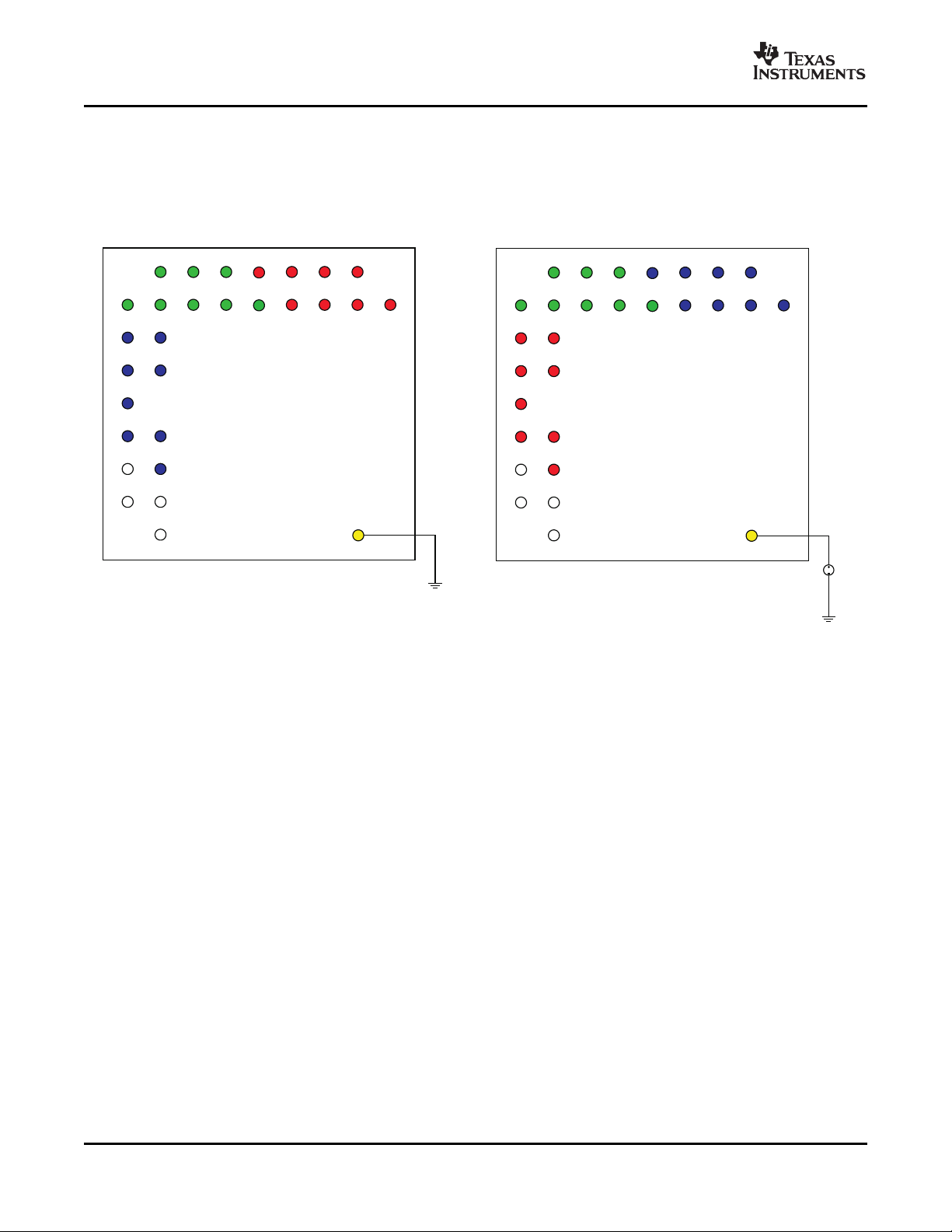
9
8764 5321
A
D
C
B
G
F
E
H
J
G0
B7
R7
B0
DE
HS VS
PCLK
B5
B1B4B2
B3
B6
R1
G6
G5G3
G2
G1 R3R6R5
R2 R4
G7
R0G4
SN65LVDS305
TopView
SWAP
SWAP=0
9
8764 5321
A
D
C
B
G
F
E
H
J
G7
R0
B0
R7
DE
HS VS
PCLK
R2
R6R3R5
R4
R1
B6
G1
G2G4
G5
G6 B4B1B2
B5 B3
G0
B7G3
SN65LVDS305
TopView
SWAP
SWAP=1
1.8V
SN65LVDS305
SLLS744A – AUGUST 2006 – REVISED JANUARY 2007
PINOUT – TOP VIEW (continued)
SWAP TERMINAL FUNCTIONALITY
The SWAP terminal allows the pcb designer to reverse the RGB bus, thus minimize potential signal crossovers
due to signal routing. Figure 1 and Figure 2 show the RGB signal terminal assignment based on the SWAP
terminal setting.
4
Figure 1. SWAP TERMINAL = 0 Figure 2. SWAP Terminal = 1
Submit Documentation Feedback
www.ti.com
SLLS744A – AUGUST 2006 – REVISED JANUARY 2007
PINOUT – TOP VIEW (continued)
Table 1. NUMERIC TERMINAL LIST
. . TERMINAL SWAP SIGNAL TERMINAL SWAP SIGNAL TERMINAL SWAP SIGNAL
A1 — GND 0 B6 0 B1
A2
A3
A4
A5
A6
A7 D1
A8 D2
0 G2 1 R1 1 R6
1 G5 0 B7 0 B2
0 G4 1 R0 1 R5
1 G3 C3 UNPOPULATED F3 — VDD
0 G6 C4 — VDD F4 — GND
1 G1 C5 — GND F5 — GND
0 R0 C6 — VDD F6 — GND
1 B7 C7 — VDD F7 — GND
0 R2 C8 — GND F8 — V
1 B5 C9 — GND F9 — NC
0 R4 0 B4 G1 — PCLK
1 B3 1 R3 0 B0
0 R6 0 B5 1 R7
1 B1 1 R2 G3 — V
A9 — GND D3 — VDD G4 — GND
B1
B2
B3
B4 E1
B5
B6
B7
B8
B9
0 G0 D4 — GND G5 — GND
1 G7 D5 — GND G6 — GND
0 G1 D6 — GND G7 — GND
1 G6 D7 — GND G8 — GND
0 G3 D8 — GND G9 — NC
1 G4 D9 — NC H1 — HS
0 G5 0 B3 H2 — VS
1 G2 1 R4 H3 — GND
0 G7 E2 — GND H4 — GND
1 G0 E3 — VDD H5 — V
0 R1 E4 — GND H6 — GND
1 B6 E5 — GND H7 — V
0 R3 E6 — GND H8 — V
1 B4 E7 — GND H9 — CPOL
0 R5 E8 — GND
1 B2 E9 — NC J2 — DE
0 R7 J3 — TXEN
1 B0 J4 — D–
C1 F1
C2 F2
PLLD
G2
J1 — GND
J5 — D+
J6 — CLK–
J7 — CLK+
J8 — SWAP
J9 — GND
SN65LVDS305
DDPLLD
DD
LVDS
LVDS
DDLVDS
PLLA
DDPLLA
DDLVDS
LVDS
Submit Documentation Feedback
5
www.ti.com
SN65LVDS305
SLLS744A – AUGUST 2006 – REVISED JANUARY 2007
Table 2. TERMINAL FUNCTIONS
NAME I/O DESCRIPTION
D+, D– SubLVDS data link (active during normal operation)
CLK+, CLK– SubLVDS output clock; clock polarity is fixed.
R0–R7 Red pixel data (8); terminal assignment depends on SWAP terminal setting.
G0–G7 Green pixel data (8); terminal assignment depends on SWAP terminal setting.
B0–B7 Blue pixel data (8); terminal assignment depends on SWAP terminal setting.
HS Horizontal sync
VS Vertical sync
DE Data enable
PCLK Input pixel clock; rising or falling clock polarity is selected by control input CPOL.
TXEN
CPOL CMOS In
SWAP CMOS In
V
DD
GND Supply ground
V
DDLVDS
GND
LVDS
V
DDPLLA
GND
PLLA
V
DDPLLD
GND
PLLD
(1) For a multilayer pcb, it is recommended to keep one common GND layer underneath the device and connect all ground terminals
directly to this plane.
SubLVDS Out
CMOS IN
Power supply
Disables the CMOS drivers and turns off the PLL, putting device in shutdown mode
1 – Transmitter enabled
0 – Transmitter disabled (shutdown)
Note: The TXEN input incorporates glitch-suppression logic to avoid device malfunction
on short input spikes. It is necessary to pull TXEN high for longer than 10 µ s to enable
the transmitter. It is necessary to pull the TXEN input low for longer than 10 µ s to
disable the transmitter. At power up, the transmitter is enabled immediately if TXEN = 1
and disabled if TXEN = 0.
Input clock polarity selection
0 – rising edge clocking
1 – falling edge clocking
Bus swap. Swaps the bus terminals to allow device placement on top or bottom of pcb.
See pinout drawing for terminal assignments.
0 – data input from B0...R7
1 – data input from R7...B0
Supply voltage
SubLVDS I/O supply voltage
(1)
SubLVDS ground
PLL analog supply voltage
PLL analog GND
PLL digital supply voltage
PLL digital GND
6
Submit Documentation Feedback
www.ti.com
D+/– CHANNEL
CLK+
B7
B6
R7
R6
R5
R4
R3
R2 R1
R0
G7 G6 G5 G4G3G2 G1 G0
B5
B4
B3
B2 B1
B0
VS HS DE
0 0
CP R7
R6
CP
00
CLK–
SN65LVDS305
SLLS744A – AUGUST 2006 – REVISED JANUARY 2007
FUNCTIONAL DESCRIPTION
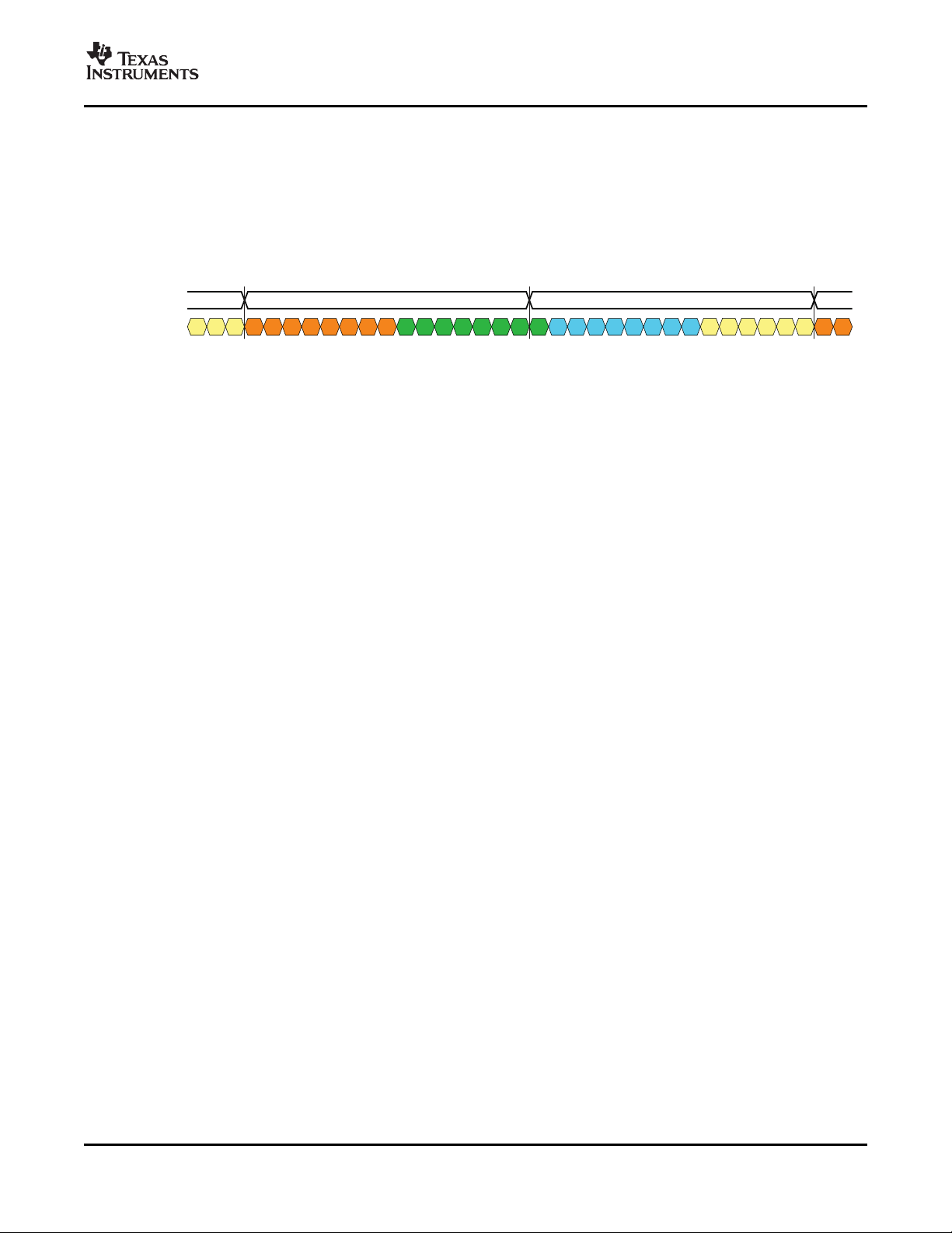
The SN65LVDS305 transmits payload data over a single SubLVDS data pair, D. The PLL locks to PCLK and
internally multiplies the clock by a factor of 30. The internal high-speed clock is used to serialize (shift out) the
data payload on D. Two reserved bits and the parity bit are added to the data frame. Figure 3 illustrates the
timing and the mapping of the data payload into the 30-bit frame. The internal high-speed clock is divided by a
factor of 30 to recreate the pixel clock, and presented on the SubLVDS CLK output. While in this mode, the PLL
can lock to a clock that is in the range of 4 MHz through 15 MHz. This is intended for smaller video display
formats (e.g. QVGA to HVGA) .
Figure 3. Data and Clock Output
Power-Down Modes
The SN65LVDS305 transmitter has two power-down modes to facilitate efficient power management.
Shutdown Mode
The SN65LVDS305 enters shutdown mode when the TXEN terminal is asserted low. This turns off all
transmitter circuitry, including the CMOS input, PLL, serializer, and SubLVDS transmitter output stage. All
outputs are high-impedance. Current consumption in shutdown mode is nearly zero.
Standby Mode
The SN65LVDS305 enters the standby mode if TXEN is high and the PCLK input signal frequency is less than
500 kHz. All circuitry except the PCLK input monitor is shut down, and all outputs enter the high-impedance
state. The current consumption in standby mode is very low. When the PCLK input signal is completely stopped,
the IDDcurrent consumption is less than 10 µ A. The PCLK input must not be left floating.
NOTE:
A floating (left open) CMOS input allows leakage currents to flow from V
to GND.
DD
To prevent large leakage current, a CMOS gate must be kept at a valid logic level,
either V
or VIL. This can be achieved by applying an external voltage of V
IH
or V
IH
to
IL
all SN65LVDS305 inputs.
Active Modes
When TXEN is high and the PCLK input clock signal is faster than 3 MHz, the SN65LVDS305 enters the active
mode. Current consumption in the active mode depends on operating frequency and the number of data
transitions in the data payload.
Acquire Mode (PLL Approaches Lock)
The PLL is enabled and attempts to lock to the input clock. All outputs remain in the high-impedance state.
When the PLL monitor detects stable PLL operation, the device switches from the acquire mode to the transmit
mode. For proper device operation, the pixel clock frequency must fall within the valid f
under recommended operating conditions. If the pixel clock frequency is larger than 3MHz but smaller than
f
(min), the SN65LVDS305 PLL is enabled. Under such conditions, it is possible for the PLL to lock
PCLK
temporarily to the pixel clock, causing the PLL monitor to release the device into transmit mode. If this happens,
the PLL may or may not be properly locked to the pixel clock input, potentially causing data errors, frequency
oscillation, and PLL deadlock (loss of VCO oscillation).
range specified
PCLK
Transmit Mode
After the PLL achieves lock, the device enters the normal transmit mode. The CLK terminal outputs a copy of
PCLK.
Submit Documentation Feedback
7
www.ti.com
Standby
Mode
Transmit
Mode
Acquire
Mode
TXENHigh>10 sm
PowerUp
TXEN=0
PowerUp
TXEN=1
CLK Active
PLL AchievedLock
Shutdown
Mode
TXENLow
>10 sm
TXENLow
>10 sm
TXENLow
>10 sm
PCLK
StopsorLost
PCLK
StopsorLost
PCLK
Active
PowerUp
TXEN=1
CLKInactive
SN65LVDS305
SLLS744A – AUGUST 2006 – REVISED JANUARY 2007
FUNCTIONAL DESCRIPTION (continued)
Parity Bit Generation
The SN65LVDS305 transmitter calculates the parity of the transmit data word and sets the parity bit accordingly.
The parity bit covers the 27-bit data payload consisting of 24 bits of pixel data plus VS, HS, and DE. The two
reserved bits are not included in the parity generation. Odd-parity bit signaling is used. The transmitter sets the
parity bit if the sum of the 27 data bits result in an even number of ones. The parity bit is cleared otherwise. This
allows the receiver to verify parity and detect single bit errors.
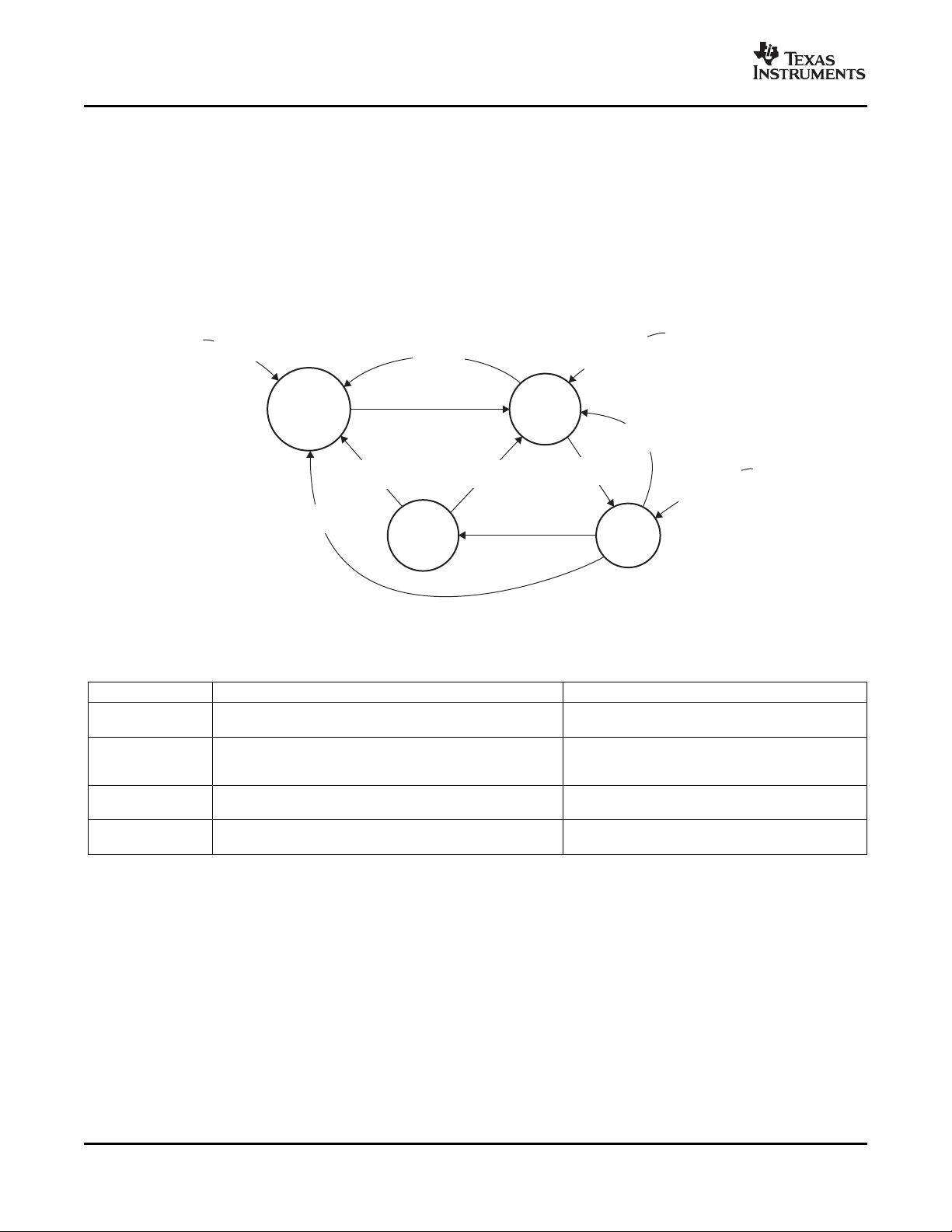
Status Detect and Operating Modes Flow diagram
The SN65LVDS305 switches between the power saving and active modes in the following way:
Figure 4. Status Detect and Operating Modes Flow Diagram
Table 3. Status Detect and Operating Modes Descriptions
Mode Characteristics Conditions
Shutdown mode Least amount of power consumption
Standby mode Low power consumption (only clock activity circuit active; PLL TXEN is high; PCLK input signal is missing or
Acquire mode PLL tries to achieve lock; all outputs are high-impedance. TXEN is high; PCLK input monitor detected input
Transmit mode Data transfer (normal operation); Transmitter serializes data TXEN is high and PLL is locked to incoming clock.
(1) In shutdown mode, all SN65LVDS305 internal switching circuits (e.g., PLL, serializer, etc.) are turned off to minimize power
consumption. The input stage of any input terminal remains active.
(2) Leaving inputs unconnected can cause random noise to toggle the input stage and potentially harm the device. All inputs must be tied to
a valid logic level, VILor VIH, during shutdown or standby mode.
8
off); all outputs are high-impedance.
is disabled to conserve power); all outputs are inactive.
high-impedance.
and transmits data on serial output.
(1)
(most circuitry turned TXEN is low.
Submit Documentation Feedback
activity.
(1) (2)
(2)
www.ti.com
SLLS744A – AUGUST 2006 – REVISED JANUARY 2007
Table 4. Operating Mode Transitions
MODE TRANSITION USE CASE TRANSITION SPECIFICS
Shutdown → standby Drive TXEN high to enable 1. TXEN high > 10 µ s
Standby → acquire Transmitter activity detected 1. PCLK input monitor detects clock input activity.
Acquire → transmit Link is ready to transfer data. 1. PLL is active and approaches lock.
Transmit → standby Request transmitter to enter 1. PCLK Input monitor detects missing PCLK.
Transmit/standby → Turn off transmitter 1. TXEN pulled low for longer than 10 µ s
shutdown
transmitter
standby mode by stopping
PCLK
2. Transmitter enters standby mode.
a. All outputs are high-impedance.
b. Transmitter turns on clock input monitor.
2. Outputs remain high-impedance.
3. PLL circuit is enabled.
2. PLL achieved lock within 2 ms.
3. Parallel data input latches into shift register .
4. CLK output turns on.
5. Selected data outputs turn on and send out first serial data bit.
2. Transmitter indicates standby, putting all outputs into high-impedance.
3. PLL shuts down.
4. PCLK activity input monitor remains active.
2. Transmitter indicates standby, putting output CLK+ and CLK– into
high-impedance state.
3. Transmitter puts all other outputs into high-impedance state.
4. Most IC circuitry is shut down for least power consumption.
SN65LVDS305
ORDERING INFORMATION
PART NUMBER PACKAGE SHIPPING METHOD
SN65LVDS305ZQER ZQE Reel
ABSOLUTE MAXIMUM RATINGS
over operating free-air temperature range (unless otherwise noted)
Supply voltage range, V
Voltage range at any input When V
or output terminal
Electrostatic discharge Charged-device model
Continuous power dissipation See Dissipation Ratings table
(1) Stresses beyond those listed under absolute maximum ratings may cause permanent damage to the device. These are stress ratings
only and functional operation of the device at these or any other conditions beyond those indicated under recommended operating
conditions is not implied. Exposure to absolute maximum-rated conditions for extended periods may affect device reliability.
(2) All voltage values are with respect to the GND terminals.
(3) In accordance with JEDEC Standard 22, Test Method A114-A.
(4) In accordance with JEDEC Standard 22, Test Method C101.
(5) In accordance with JEDEC Standard 22, Test Method A115-A
DD
(2)
, V
When V
Human-body model
Machine model
, V
DDPLLA
DDx
DDx
(1)
VALUE UNIT
, V
DDPLLD
DDLVDS
–0.3 to 2.175 V
> 0 V –0.5 to 2.175 V
≤ 0 V –0.5 to V
(3)
(all terminals) ± 3 kV
(4)
(all terminals) ± 500
(5)
(all terminals) ± 200
+ 2.175 V
DD
V
Submit Documentation Feedback
9
 Loading...