

SN65LVDS2
HIGH-SPEED DIFFERENTIAL LINE RECEIVER
SLLS406 – DECEMBER 1999
D Meets or Exceeds ANSI TIA/EIA-644
Standard
D Designed for Signaling Rates up to
400 Mbps
D Operates From a 2.4-V to 3.6-V Supply
D Available in the SOT-23 Package
D Differential Input Voltage Threshold Less
V
CC
GND
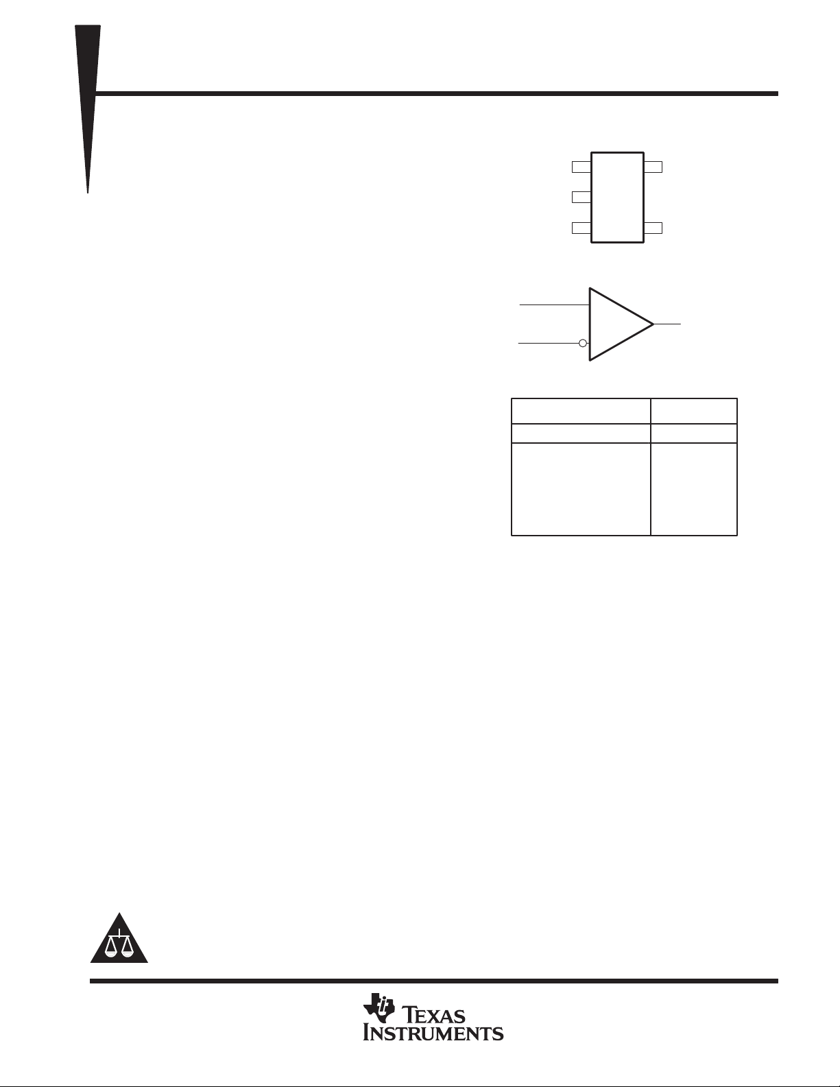
SN65LVDS2
DBV PACKAGE
(TOP VIEW)
1
2
3
A
5
R
4
B
Than 100 mV
D Propagation Delay Times, 2.5 ns Typical
logic diagram
D Power Dissipation at 200 MHz Is Typically
60 mW
D Bus-Pin ESD Protection Exceeds 15 kV
D Open-Circuit Fail Safe
D Output is High Impedance With V
description
The SN65L VDS2 is a single low-voltage dif ferential line receiver in a small-outline transistor
package. The inputs comply with the TIA/EIA-644
standard and provide a maximum differential input
threshold of 100 mV over an input common-mode
voltage range of 0 V to 2.4 V.
When used with a low-voltage differential
signaling (L VDS) driver (such as the SN65LVDS1)
in a point-to-point or multidrop configuration; data
or clocking signals can be transmitted over printed-circuit board traces or cables at very high rates with very
low electromagnetic emissions and power consumption.
CC
< 1.5 V
3
A
B
4
5
R
Function Table
INPUTS OUTPUT
VID = VA – V
VID ≥ 100 mV
–100 mV < VID < 100 mV
VID ≤ –100 mV
Open H
H = high level, L = low level , ? = indeterminate
B
R
H
?
L
The high-speed switching of LVDS signals requires the use of a line impedance matching resistor at the
receiving-end of the cable or transmission media. TI offers you both the SN65LVDS2, which requires this
external resistor, or its companion the SN65L VDT2, which eliminates the need by integrating it with the receiver .
The packaging, low power, low EMI, high ESD tolerance, and wide supply voltage range make these devices
ideal for battery-powered applications.
The SN65LVDS2 is characterized for operation from –40°C to 85°C.
Please be aware that an important notice concerning availability, standard warranty, and use in critical applications of
Texas Instruments semiconductor products and disclaimers thereto appears at the end of this data sheet.
PRODUCTION DATA information is current as of publication date.
Products conform to specifications per the terms of Texas Instruments
standard warranty. Production processing does not necessarily include
testing of all parameters.
Copyright 1999, Texas Instruments Incorporated
POST OFFICE BOX 655303 • DALLAS, TEXAS 75265
1
SN65LVDS2
Common mode in ut voltage, V
IC
(see Figure 6)
V
HIGH-SPEED DIFFERENTIAL LINE RECEIVER
SLLS406 – DECEMBER 1999
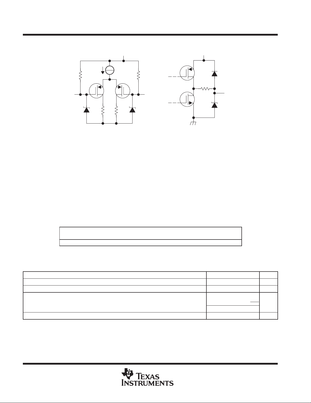
equivalent input and output schematic diagrams
V
CC
300 kΩ300 kΩ
B InputA Input
7 V
7 V
absolute maximum ratings over operating free-air temperature (unless otherwise noted)
V
CC
5 Ω
R Output
7 V
†
Supply voltage range, VCC (see Note 1) –0.5 V to 4 V. . . . . . . . . . . . . . . . . . . . . . . . . . . . . . . . . . . . . . . . . . . . . .
Voltage range (A, B, or R) –0.5 V to VCC+ 0.5 V. . . . . . . . . . . . . . . . . . . . . . . . . . . . . . . . . . . . . . . . . . . . . . . . . . . .
Electrostatic discharge: A, B , and GND (see Note 2) CLass 3, A:15 kV, B:600 V. . . . . . . . . . . . . . . . . . . . . . .
R (see Note 2) CLass 3, A:7 kV, B:500 V. . . . . . . . . . . . . . . . . . . . . . . . . . . . . . . . . . . . .
Continuous total power dissipation See dissipation rating table. . . . . . . . . . . . . . . . . . . . . . . . . . . . . . . . . . . . . . .
Storage temperature range –65°C to 150°C. . . . . . . . . . . . . . . . . . . . . . . . . . . . . . . . . . . . . . . . . . . . . . . . . . . . . . . .
Lead temperature 1,6 mm (1/16 inch) from case for 10 seconds 250°C. . . . . . . . . . . . . . . . . . . . . . . . . . . . . . .
†
Stresses beyond those listed under “absolute maximum ratings” may cause permanent damage to the device. These are stress ratings only, and
functional operation of the device at these or any other conditions beyond those indicated under “recommended operating conditions” is not
implied. Exposure to absolute-maximum-rated conditions for extended periods may affect device reliability.
NOTES: 1. All voltage values, except differential I/O bus voltages are with respect to network ground terminal.
2. Tested in accordance with MIL-STD-883C Method 3015.7.
DISSIPATION RATING TABLE
PACKAGE
DBV 385 mW 3.1 mW/°C 200 mW
†
This is the inverse of the junction-to-ambient thermal resistance when board-mounted (low-K) and with
no air flow.
TA ≤ 25°C
POWER RATING
DERATING FACTOR
ABOVE TA = 25°C
†
TA = 85°C
POWER RATING
recommended operating conditions
MIN NOM MAX UNIT
Supply voltage, V
Magnitude of differential input voltage, VID 0.1 0.6 V
Common–mode input voltage, VIC (see Figure 6)
Operating free–air temperature, T
CC
A
2.4 3.3 3.6 V
Ť
Ť
0
–40 85 °C
2.4 *
VCC–0.8
V
ID
V
2
POST OFFICE BOX 655303 • DALLAS, TEXAS 75265
HIGH-SPEED DIFFERENTIAL LINE RECEIVER
S
3
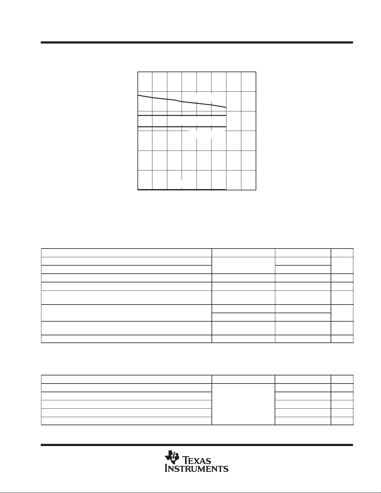
COMMON-MODE INPUT VOLTAGE
vs
DIFFERENTIAL INPUT VOLTAGE
3
SN65LVDS2
SLLS406 – DECEMBER 1999
2.5
2
1.5
1
– Common-Mode Input Voltage – V
0.5
IC
V
0
0
MIN
0.1 0.3
0.2 0.4 0.6
|VID|– Differential Input Voltage – V
Figure 1. VIC vs VID and V
VCC = 3.6 V
VCC = 2.7 V
VCC = 2.4 V
0.5
0.80.7
CC
electrical characteristics over recommended operating conditions, VCC = 2.4 to 3 V (unless
otherwise noted)
PARAMETER TEST CONDITIONS MIN TYP†MAX UNIT
V
ITH+
V
ITH–
V
OH
V
OL
I
CC
I
I
I
ID
I
I(OFF)
†
All typical values are at 25°C and with a 2.7-V supply.
Positive-going differential input voltage threshold
Negative-going differential input voltage threshold
High-level output voltage IOH = –8 mA 1.9 2.4 V
Low-level output voltage IOL = 8 mA 0.25 0.4 V
Supply current
Input current (A or B inputs)
Differential input current (IIA – IIB)
Power-off input current (A or B inputs) VCC = 0 V, VI = 2.4 V ±20 µA
See Figure 2 and Table 1
No load,
Steady state
VI = 0 V ±20
VI = 2.4 V or VCC – 0.8
VIA = 0 V, VIB = 0.1 V
VIA = 2.4 V VIB = 2.3 V,
–100
–1.2
100
mV
4 7 mA
µA
±2 µA
receiver switching characteristics over recommended operating conditions, VCC = 2.4 to 2.7 V
(unless otherwise noted)
PARAMETER TEST CONDITIONS MIN TYP†MAX UNIT
t
PLH
t
PHL
t
sk(p)
t
r
t
f
†
All typical values are at 25°C and with a 2.7-V.
‡
t
sk(p)
Propagation delay time, low-to-high-level output 1.4 2.6 3.6 ns
Propagation delay time, high-to-low-level output
Pulse skew (|t
Output signal rise time
Output signal fall time 0.8 1.4 ns
is the magnitude of the time difference between the high-to-low and low-to-high propagation delay times at an output.
pHL
– t
pLH
‡
|)
POST OFFICE BOX 655303 • DALLAS, TEXAS 75265
CL = 10 pF,
ee Figure
1.4 2.5 3.6 ns
0.1 0.6 ns
0.8 1.4 ns
3

SN65LVDS2
S
3
HIGH-SPEED DIFFERENTIAL LINE RECEIVER
SLLS406 – DECEMBER 1999
electrical characteristics over recommended operating conditions, VCC = 3 V to 3.6 V (unless
otherwise noted)
PARAMETER TEST CONDITIONS MIN TYP†MAX UNIT
V
ITH+
V
ITH–
V
OH
V
OL
I
CC
I
I
I
ID
I
I(OFF)
†
All typical values are at 25°C and with a 3.3-V supply.
receiver switching characteristics over recommended operating conditions, VCC = 3 V to 3.6 V
(unless otherwise noted)
t
PLH
t
PHL
t
sk(p)
t
r
t
f
†
All typical values are at 25°C and with a 3.3-V.
‡
t
sk(p)
Positive-going differential input voltage threshold
Negative-going differential input voltage threshold
High-level output voltage IOH = –8 mA 2.4 3 V
Low-level output voltage IOL = 8 mA 0.25 0.4 V
Supply current
Input current (A or B inputs)
Differential input current (IIA – IIB)
Power-off input current (A or B inputs) VCC = 0 V, VI = 2.4 V 20 µA
PARAMETER TEST CONDITIONS MIN TYP†MAX UNIT
Propagation delay time, low-to-high-level output 1.4 2.6 3.1 ns
Propagation delay time, high-to-low-level output
Pulse skew (|t
Output signal rise time
Output signal fall time 0.7 1.1 ns
is the magnitude of the time difference between the high-to-low and low-to-high propagation delay times at an output.
pHL
– t
pLH
‡
|)
See Figure 2 and Table 1
No load,
Steady state
VI = 0 V ±20
VI = 2.4 V
VIA = 0 V, VIB = 0.1 V
VIA = 2.4 V VIB = 2.3 V,
CL = 10 pF,
ee Figure
–100
–1.2
1.4 2.5 3.1 ns
100
5 8 mA
0.1 0.5 ns
0.7 1.1 ns
mV
µA
±2 µA
4
POST OFFICE BOX 655303 • DALLAS, TEXAS 75265
HIGH-SPEED DIFFERENTIAL LINE RECEIVER
PARAMETER MEASUREMENT INFORMATION
A
SN65LVDS2
SLLS406 – DECEMBER 1999
VIA V
2
IB
V
IA
V
IC
V
ID
B
V
IB
R
V
O
Figure 2. Receiver Voltage Definitions
Table 1. Receiver Minimum and Maximum Input Threshold Test Voltages
APPLIED VOLTAGES
V
1.25 1.15 100 1.2
1.15 1.25 –100 1.2
(V)
IA
2.4 2.3 100 2.35
2.3 2.4 –100 2.35
0.1 0 100 0.05
0 0.1 –100 0.05
1.5 0.9 600 1.2
0.9 1.5 –600 1.2
2.4 1.8 600 2.1
1.8 2.4 –600 2.1
0.6 0 600 0.3
0 0.6 –600 0.3
V
IB
RESULTING DIFFERENTIAL
INPUT VOLTAGE
(mV)
V
ID
RESULTING COMMON-
MODE INPUT VOLTAGE
V
(V)
IC
POST OFFICE BOX 655303 • DALLAS, TEXAS 75265
5

SN65LVDS2
HIGH-SPEED DIFFERENTIAL LINE RECEIVER
SLLS406 – DECEMBER 1999
PARAMETER MEASUREMENT INFORMATION
V
ID
V
IA
V
IB
C
L
10 pF
V
O
V
IA
V
IB
V
ID
t
PHL
V
O
V
O
NOTE A: All input pulses are supplied by a generator having the following characteristics: tr or tf ≤ 1 ns, pulse repetition rate (PRR) = 50 Mpps,
pulse width = 10 ± 0.2 ns. CL includes instrumentation and fixture capacitance within 0,06 m of the D.U.T.
2.4 V
0.4 V
80%
20%
t
f
t
f
t
PLH
t
r
t
r
1.4 V
1 V
0.4 V
0 V
–0.4 V
V
OH
1.4 V
V
OL
V
OH
1.2 V
V
OL
With VCC = 3.3 V
With VCC = 2.7 V
Figure 3. Timing Test Circuit and Waveforms
6
POST OFFICE BOX 655303 • DALLAS, TEXAS 75265

HIGH-SPEED DIFFERENTIAL LINE RECEIVER
TYPICAL CHARACTERISTICS
SN65LVDS2
SLLS406 – DECEMBER 1999
4
3.5
3
2.5
2
1.5
1
– High-Level Output Voltage – V
OH
V
0.5
0
–70
2.9
HIGH-LEVEL OUTPUT VOLTAGE
vs
HIGH-LEVEL OUTPUT CURRENT
VCC = 3.3 V
VCC = 2.7 V
–40–50 –30–60
IOH – High-Level Output Current – mA
–20
–10
Figure 4
HIGH-TO-LOW LEVEL
PROPAGATION DELAY TIMES
vs
FREE-AIR TEMPERATURE
LOW-LEVEL OUTPUT VOLTAGE
vs
4
3.5
3
2.5
2
1.5
1
– Low-Level Output Voltage – V
OL
V
0.5
0
0
LOW-LEVEL OUTPUT CURRENT
VCC = 2.7 V
0
IOL – Low-Level Output Current – mA
3020 4010 50
VCC = 3.3 V
60
70
Figure 5
LOW-TO-HIGH LEVEL
PROPAGATION DELAY TIME
vs
FREE-AIR TEMPERATURE
3
2.85
2.8
2.75
2.7
2.65
2.6
2.55
2.5
2.45
– High-to-Low Level Propagation Delay Time – ns
2.4
PHL
t
VCC = 2.4 V
VCC = 3.6 V
VCC = 3.3 V
VCC = 2.7 V
–20 0 40–40
TA – Free-Air Temperature – °C
20
Figure 6
VCC = 3 V
60 80
2.9
2.8
2.7
2.6
2.5
2.4
2.3
– Low-to-High Level Propagation Delay Time – ns
2.2
PLH
t
VCC = 3.3 V
VCC = 3.6 V
VCC = 3 V
VCC = 2.7 V
–20 0 40–40
TA – Free-Air Temperature – °C
20 60 80 100
Figure 7
VCC = 2.4 V
POST OFFICE BOX 655303 • DALLAS, TEXAS 75265
7

SN65LVDS2
HIGH-SPEED DIFFERENTIAL LINE RECEIVER
SLLS406 – DECEMBER 1999
APPLICATION INFORMATION
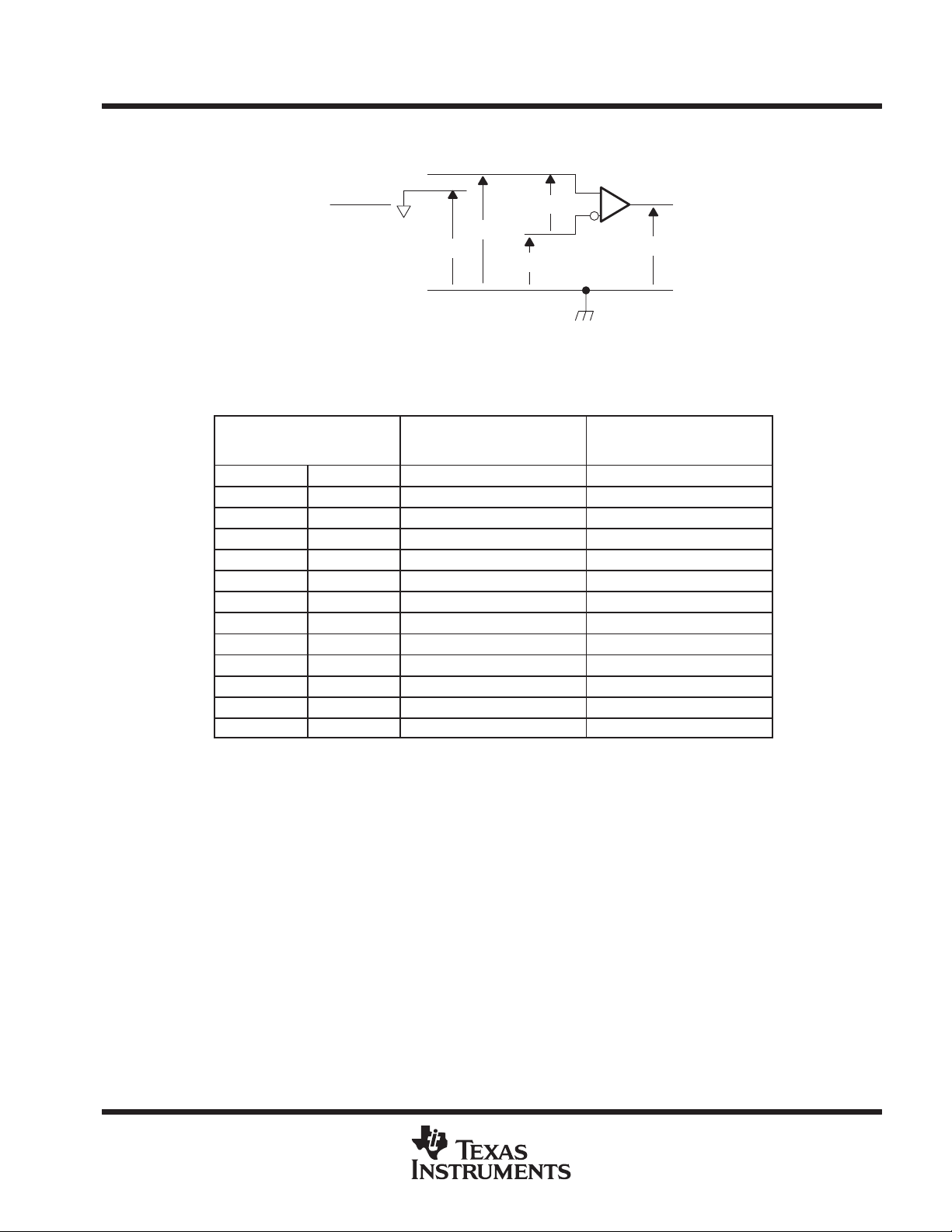
fail safe
One of the most common problems with differential signaling applications is how the system responds when
no differential voltage is present on the signal pair . The LVDS receiver is like most differential line receivers, in
that its output logic state can be indeterminate when the differential input voltage is between –100 mV and 100
mV and within its recommended input common-mode voltage range. TI’s LVDS receiver is different in how it
handles the open-input circuit situation, however.
Open-circuit means that there is little or no input current to the receiver from the data line itself. This could be
when the driver is in a high-impedance state or the cable is disconnected. When this occurs, the L VDS receiver
will pull each line of the signal pair to near V
feature uses an AND gate with input voltage thresholds at about 2.3 V to detect this condition and force the
output to a high-level regardless of the differential input voltage.
300 kΩ 300 kΩ
through 300-kΩ resistors as shown in Figure 10. The fail-safe
CC
V
CC
A
Rt = 100 Ω (Typ)
B
VIT ≈ 2.3 V
Y
Figure 8. Open-Circuit Fail Safe of the LVDS Receiver
It is only under these conditions that the output of the receiver will be valid with less than a 100 mV differential
input voltage magnitude. The presence of the termination resistor, Rt, does not af fect the fail-safe function as
long as it is connected as shown in the figure. Other termination circuits may allow a dc current to ground that
could defeat the pullup currents from the receiver and the fail-safe feature.
8
POST OFFICE BOX 655303 • DALLAS, TEXAS 75265

SN65LVDS2
HIGH-SPEED DIFFERENTIAL LINE RECEIVER
SLLS406 – DECEMBER 1999
MECHANICAL INFORMATION
DBV (R-PDSO-G5) PLASTIC SMALL-OUTLINE
0,95
1,45
0,95
3,00
2,80
45
31
0,05 MIN
0,50
0,30
1,70
1,50
M
0,20
3,00
2,60
Seating Plane
0,10
0,15 NOM
Gage Plane
0°–8°
0,25
0,55
0,35
NOTES: A. All linear dimensions are in millimeters.
B. This drawing is subject to change without notice.
C. Body dimensions do not include mold flash or protrusion.
D. Falls within JEDEC MO-178
4073253-4/E 05/99
POST OFFICE BOX 655303 • DALLAS, TEXAS 75265
9

IMPORTANT NOTICE
T exas Instruments and its subsidiaries (TI) reserve the right to make changes to their products or to discontinue
any product or service without notice, and advise customers to obtain the latest version of relevant information
to verify, before placing orders, that information being relied on is current and complete. All products are sold
subject to the terms and conditions of sale supplied at the time of order acknowledgement, including those
pertaining to warranty, patent infringement, and limitation of liability.
TI warrants performance of its semiconductor products to the specifications applicable at the time of sale in
accordance with TI’s standard warranty. Testing and other quality control techniques are utilized to the extent
TI deems necessary to support this warranty . Specific testing of all parameters of each device is not necessarily
performed, except those mandated by government requirements.
CERTAIN APPLICA TIONS USING SEMICONDUCTOR PRODUCTS MA Y INVOLVE POTENTIAL RISKS OF
DEATH, PERSONAL INJURY, OR SEVERE PROPERTY OR ENVIRONMENTAL DAMAGE (“CRITICAL
APPLICATIONS”). TI SEMICONDUCTOR PRODUCTS ARE NOT DESIGNED, AUTHORIZED, OR
WARRANTED TO BE SUITABLE FOR USE IN LIFE-SUPPORT DEVICES OR SYSTEMS OR OTHER
CRITICAL APPLICA TIONS. INCLUSION OF TI PRODUCTS IN SUCH APPLICATIONS IS UNDERST OOD TO
BE FULLY AT THE CUSTOMER’S RISK.
In order to minimize risks associated with the customer’s applications, adequate design and operating
safeguards must be provided by the customer to minimize inherent or procedural hazards.
TI assumes no liability for applications assistance or customer product design. TI does not warrant or represent
that any license, either express or implied, is granted under any patent right, copyright, mask work right, or other
intellectual property right of TI covering or relating to any combination, machine, or process in which such
semiconductor products or services might be or are used. TI’s publication of information regarding any third
party’s products or services does not constitute TI’s approval, warranty or endorsement thereof.
Copyright 1999, Texas Instruments Incorporated
 Loading...