

Page 1
D
PCI Bus Power Management Interface
Specification 1.0 Compliant
D
ACPI 1.0 Compliant
D
Fully Compatible With the Intel 430TX
(Mobile Triton II) Chipset
D
Packaged in a 208-Pin Low-Profile QFP
(PDV) or GHK High Density Ball Grid Array
(BGA)
D
PCI Local Bus Specification Revision 2.2
Compliant
D
1997 PC Card Standard Compliant
D
PC 99 Compliant
D
3.3-V Core Logic With Universal PCI
Interfaces Compatible With 3.3-V and 5-V
PCI Signaling Environments
D
Mix-and-Match 5-V/3.3-V 16-bit PC Cards
and 3.3-V CardBus Cards
D
Supports Two PC Card or CardBus Slots
With Hot Insertion and Removal
D
Uses Serial Interface to TI TPS2202/2206
Dual-Slot PC Card Power Switch
D
Supports Burst Transfers to Maximize Data
Throughput on the PCI Bus and CardBus
Bus
D
Supports Parallel PCI Interrupts, Parallel
ISA IRQ and Parallel PCI Interrupts, Serial
ISA IRQ With Parallel PCI Interrupts, and
Serial ISA IRQ and PCI Interrupts
Description 2. . . . . . . . . . . . . . . . . . . . . . . . . . . . . . . . . . . . . . . . . . . .
System Block Diagram 3. . . . . . . . . . . . . . . . . . . . . . . . . . . . . . . . . .
Terminal Assignments 4. . . . . . . . . . . . . . . . . . . . . . . . . . . . . . . . . . .
Signal Name/Terminal Number Sort Tables 6. . . . . . . . . . . . . . . . .
Terminal Functions 12. . . . . . . . . . . . . . . . . . . . . . . . . . . . . . . . . . . .
Power Supply Sequencing 22. . . . . . . . . . . . . . . . . . . . . . . . . . . . . .
I/O Characteristics 22. . . . . . . . . . . . . . . . . . . . . . . . . . . . . . . . . . . . .
Clamping Voltages 22. . . . . . . . . . . . . . . . . . . . . . . . . . . . . . . . . . . . .
Peripheral Component Interconnect (PCI) Interface 23. . . . . . . .
PC Card Applications 24. . . . . . . . . . . . . . . . . . . . . . . . . . . . . . . . . .
Serial Bus Interface 29. . . . . . . . . . . . . . . . . . . . . . . . . . . . . . . . . . . .
Programmable Interrupt Subsystem 34. . . . . . . . . . . . . . . . . . . . . .
Power Management Overview 39. . . . . . . . . . . . . . . . . . . . . . . . . .
PC Card Controller Programming Model 44. . . . . . . . . . . . . . . . . .
PCI Configuration Registers (Functions 0 and 1) 44. . . . . . . . . . .
ExCA Compatibility Registers (Functions 0 and 1) 80. . . . . . . . .
D
D
D
D
D
D
D
D
D
D
D
D
D
Table of Contents
CardBus Socket Registers (Functions 0 and 1) 103. . . . . . . . . . . . . .
Absolute Maximum Ratings 111. . . . . . . . . . . . . . . . . . . . . . . . . . . . . . .
Recommended Operating Conditions 112. . . . . . . . . . . . . . . . . . . . . .
Electrical Characteristics 113. . . . . . . . . . . . . . . . . . . . . . . . . . . . . . . . .
PCI Clock/Reset Timing Requirements 114. . . . . . . . . . . . . . . . . . . . .
PCI Timing Requirements 114. . . . . . . . . . . . . . . . . . . . . . . . . . . . . . . .
Parameter Measurement Information 115. . . . . . . . . . . . . . . . . . . . . . .
PCI Bus Parameter Measurement Information 116. . . . . . . . . . . . . . .
PC Card Cycle Timing 117. . . . . . . . . . . . . . . . . . . . . . . . . . . . . . . . . . .
Timing Requirements (Memory Cycles) 118. . . . . . . . . . . . . . . . . . . . .
Timing Requirements (I/O Cycles) 118. . . . . . . . . . . . . . . . . . . . . . . . .
Switching Characteristics (Miscellaneous 119. . . . . . . . . . . . . . . . . . .
PC Card Parameter Measurement Information 120. . . . . . . . . . . . . . .
Mechanical Data 121. . . . . . . . . . . . . . . . . . . . . . . . . . . . . . . . . . . . . . . .
PCI1221 GHK/PDV
PC CARD CONTROLLERS
SCPS042 – JULY 1998
Pipelined Architecture Allows Greater Than
130M-Bps Throughput From
CardBus-to-PCI and From PCI-to-CardBus
Supports Up to Five General-Purpose I/Os
Serial EEPROM Interface for Loading
Subsystem ID and Subsystem Vendor ID
Programmable Output Select for CLKRUN
Multifunction PCI Device With Separate
Configuration Space for Each Socket
Five PCI Memory Windows and T wo I/O
Windows Available for Each R2 Socket
Two I/O Windows and Two Memory
Windows Available to Each CardBus
Socket
Exchangeable Card Architecture (ExCA)
Compatible Registers Are Mapped in
Memory and I/O Space
Intel 82365SL-DF Register Compatible
Supports Ring Indicate, SUSPEND, PCI
CLKRUN, and CardBus CCLKRUN
LED Activity Pins
Supports PCI Bus Lock (LOCK)
Advanced Submicron, Low-Power CMOS
T echnology
ADVANCE INFORMATION
Please be aware that an important notice concerning availability, standard warranty, and use in critical applications of
Texas Instruments semiconductor products and disclaimers thereto appears at the end of this data sheet.
PC Card is a trademark of Personal Computer Memory Card International Association (PCMCIA).
Intel is a trademark of Intel Corporation.
TI is a trademark of Texas Instruments Incorporated.
ADVANCE INFORMATION concerns new products in the sampling or
preproduction phase of development. Characteristic data and other
specifications are subject to change without notice.
POST OFFICE BOX 655303 • DALLAS, TEXAS 75265
Copyright 1998, Texas Instruments Incorporated
1
Page 2

PCI1221 GHK/PDV
PC CARD CONTROLLERS
SCPS042 – JUL Y 1998
description
The TI PCI1221 is a high-performance PCI-to-PC Card controller that supports two independent card sockets
compliant with the 1997 PC Card Standard. The PCI1221 provides a rich feature set that makes it the best
choice for bridging between PCI and PC Cards in both notebook and desktop computers. The 1997 PC Card
Standard retains the 16-bit PC Card specification defined in PCMCIA Release 2.2 and defines the new 32-bit
PC Card, CardBus, capable of full 32-bit data transfers at 33 MHz. The PCI1221 supports any combination of
16-bit and CardBus PC Cards in the two sockets, powered at 5 V or 3.3 V, as required.
The PCI1221 is compliant with the PCI Local Bus Specification 2.2, and its PCI interface can act as either a PCI
master device or a PCI slave device. The PCI bus mastering is initiated during CardBus PC Card bridging
transactions. The PCI1221 is also compliant with the latest
All card signals are internally buffered to allow hot insertion and removal without external buffering. The PCI1221
is register compatible with the Intel 82365SL-DF ExCA controller. The PCI1221 internal data path logic allows
the host to access 8-, 16-, and 32-bit cards using full 32-bit PCI cycles for maximum performance. Independent
buffering and a pipeline architecture provide an unsurpassed performance level with sustained bursting. The
PCI1221 can also be programmed to accept fast posted writes to improve system-bus utilization.
Multiple system-interrupt signaling options are provided, including: parallel PCI, parallel ISA, serialized ISA, and
serialized PCI. Furthermore, general-purpose inputs and outputs are provided for the board designer to
implement sideband functions. Many other features designed into the PCI1221, such as socket activity
light-emitting diode (LED) outputs, are discussed in detail throughout the design specification.
PCI Bus Power Management Interface Specification
.
An advanced complementary metal-oxide semiconductor (CMOS) process is used to achieve low
system-power consumption while operating at PCI clock rates up to 33 MHz. Several low-power modes enable
the host power management system to further reduce power consumption.
Unused PCI1221 inputs must be pulled up using a 43kW-resistor.
2
POST OFFICE BOX 655303 • DALLAS, TEXAS 75265
Page 3
PCI1221 GHK/PDV
PC CARD CONTROLLERS
SCPS042 – JULY 1998
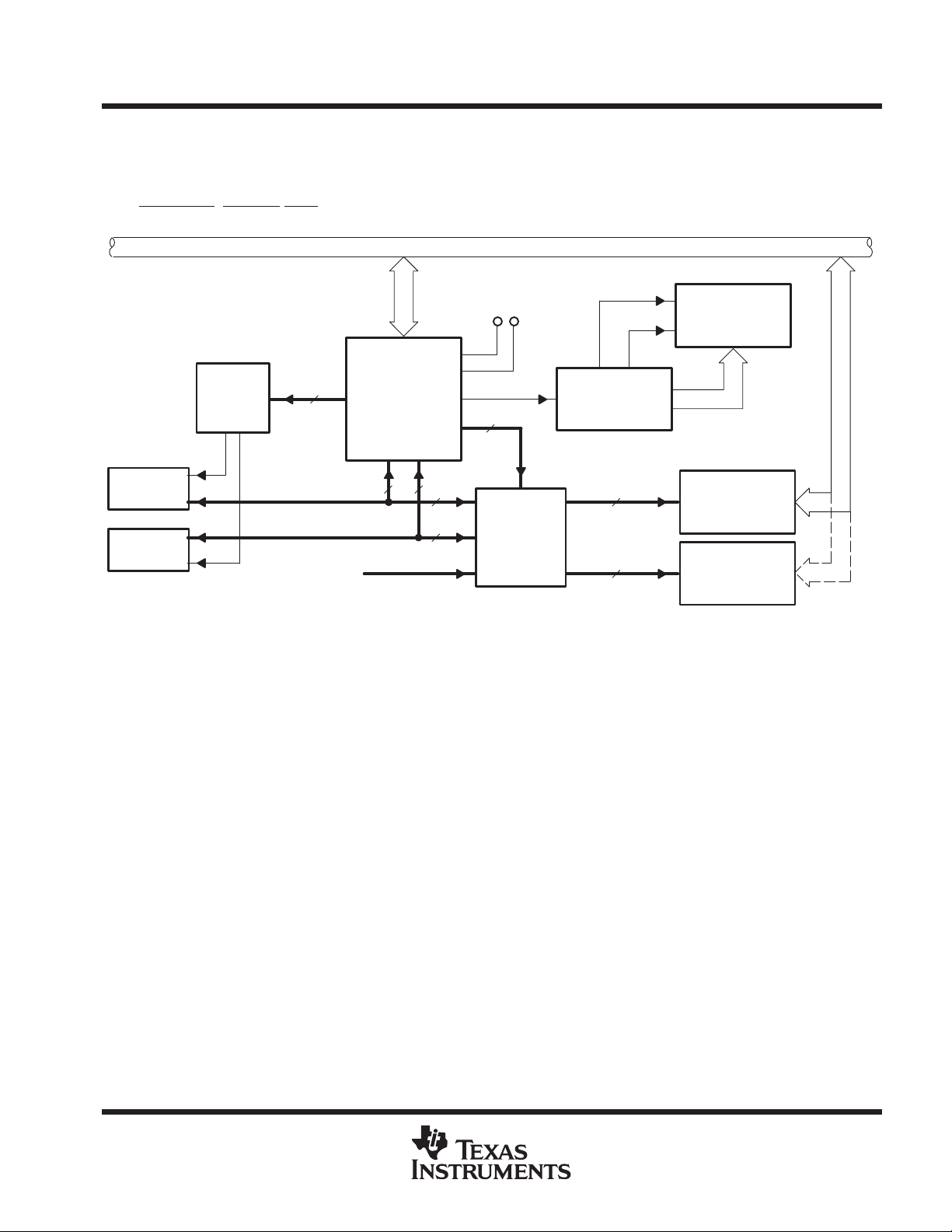
system block diagram
A simplified block diagram of the PCI1221 is provided below. The PCI interface includes all address/data and
control signals for PCI protocol. The interrupt interface includes terminals for parallel PCI, parallel ISA, and
serialized PCI and ISA signaling. Miscellaneous system interface terminals include multifunction terminals:
SUSPEND
, RI_OUT/PME (power management control signal), and SPKROUT.
PCI Bus
Activity LED’s
TPS2206
Power
Switch
PC Card
Socket A
PC Card
Socket B
External ZV Port
NOTE: The PC Card interface is 68 pins for CardBus and 16-bit PC Cards. In zoomed-video mode 23 pins are used for routing the zoomed
video signals to the VGA controller.
3
PCI1221
68 68
23
23
IRQSER
3
PCI930
ZV Switch
PCI950
IRQSER
Deserializer
Zoom Video
Zoom Video
INTA
INTB
19
4
Interrupt
Controller
IRQ2–15
VGA
Controller
Audio
Sub-System
POST OFFICE BOX 655303 • DALLAS, TEXAS 75265
3
Page 4
PCI1221 GHK/PDV
PC CARD CONTROLLERS
SCPS042 – JUL Y 1998
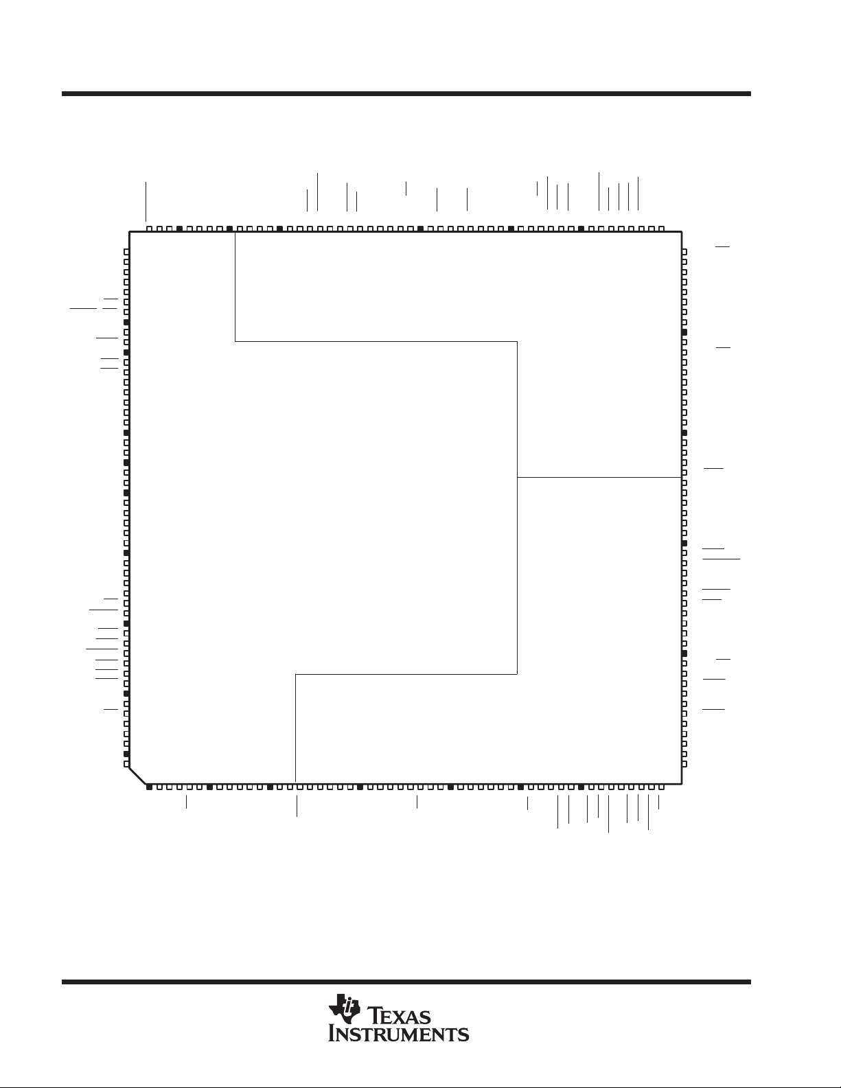
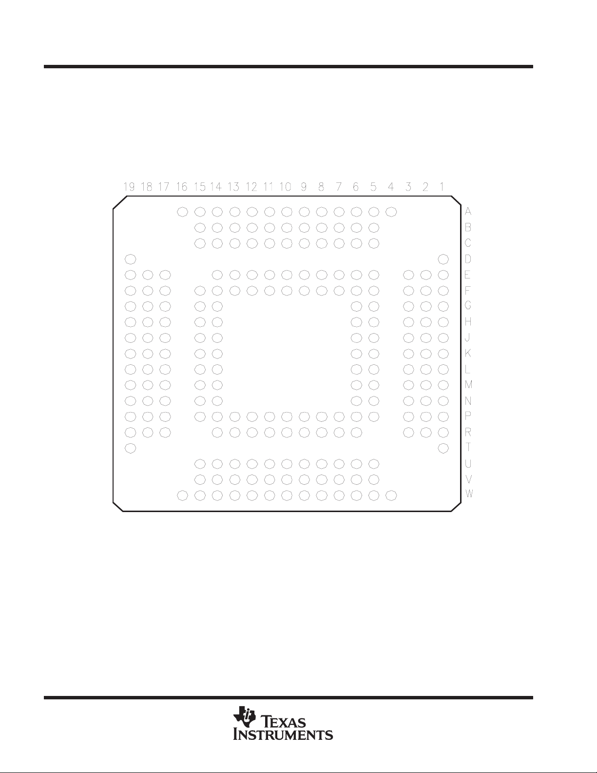
terminal assignments
PDV LOW-PROFILE QUAD FLAT PACKAGE
TOP VIEW
MFUNC2
MFUNC3
MFUNC4
MFUNC5
MFUNC6
C/BE3
RI_OUT/PME
V
CC
AD25
PRST
GND
GNT
REQ
AD31
AD30
AD11
AD29
AD28
V
CC
AD27
AD26
V
CCP
AD24
PCLK
GND
IDSEL
AD23
AD22
AD21
AD20
V
CC
AD19
AD18
AD17
AD16
C/BE2
FRAME
GND
IRDY
TRDY
DEVSEL
STOP
PERR
SERR
V
CC
PAR
C/BE1
AD15
AD14
AD13
GND
AD12
SUSPEND
GND
MFUNC0
DATA
SPKROUT
LATCH
CLOCK
152
151
150
149
VCCI
148
MFUNC1
154
153
156
155
157
158
159
160
161
162
163
164
165
166
167
168
169
170
171
172
173
174
175
176
177
178
179
180
181
182
183
184
185
186
187
188
189
190
191
192
193
194
195
196
197
198
199
200
201
202
203
204
205
206
207
208
214365871091211141316151817201922212423262528273029323134333635383740394241444346454847504952
A_CAD31
A_CAD30
A_RSVD
146
145
147
V
A_CAD28
A_CAD29
A_CAD27
142
141
144
143
PCI1221 Core
A_CCD2
A_CCLKRUN
A_CSTSCHG
138
140
139
A_CAUDIO
137
CC
A_CINT
A_CSERR
A_CVS1
134
136
135
A_CAD25
A_CAD26
A_CAD24
132
131
133
A_CC/BE3
A_CAD23
GND
128
130
129
Card A
A_CAD21
A_CAD22
A_CREQ
126
125
127
A_CRST
124
A_CAD20
A_CAD19
A_CVS2
122
121
123
Card B
CCA
V
A_CAD18
119
120
A_CC/BE2
A_CAD17
118
117
CC
A_CFRAME
A_CTRDY
A_CIRDY
114
113
116
115
A_CCLKVA_CDEVSEL
112
A_CGNT
111
110
A_CSTOP
A_CBLOCK
A_CPERR
108
107
109
A_RSVD
A_CPAR
105
104
103
102
101
100
51 106
99
98
97
96
95
94
93
92
91
90
89
88
87
86
85
84
83
82
81
80
79
78
77
76
75
74
73
72
71
70
69
68
67
66
65
64
63
62
61
60
59
58
57
56
55
54
53
A_CC/BE1
A_CAD16
A_CAD14
A_CAD15
A_CAD12
A_CAD13
A_CAD11
A_CAD10
GND
A_CAD9
A_CC/BE0
A_CAD8
A_CAD7
A_RSVD
A_CAD5
A_CAD6
A_CAD3
A_CAD4
V
CC
A_CAD1
A_CAD2
A_CAD0
A_CCD1
B_CAD31
B_RSVD
B_CAD30
B_CAD29
B_CAD28
B_CAD27
GND
B_CCD2
B_CCLKRUN
B_CSTSCHG
B_CAUDIO
B_CSERR
B_CINT
B_CVS1
B_CAD26
B_CAD25
B_CAD24
V
CC
B_CC/BE3
B_CAD23
B_CREQ
B_CAD22
B_CAD21
B_CRST
B_CAD20
B_CVS2
B_CAD19
B_CAD18
B_CAD17
CCP
V
AD10
AD9
AD8
AD7
C/BE0
CC
AD4
AD6
AD5
AD3
AD1
AD0
V
AD2
GND
B_CAD0
B_CAD2
B_CCD1
B_CAD1
B_CAD4
B_CAD3
GND
B_CAD6
B_CAD5
B_CAD7
B_RSVD
B_CAD8
B_CAD9
B_CAD10
B_CC/BE0
CC
V
B_CAD11
B_CAD13
B_CAD14
B_CAD12
B_CAD15
CCB
V
B_CAD16
B_CC/BE1
B_CPAR
B_RSVD
B_CBLOCK
GND
B_CSTOP
B_CPERR
B_CCLK
B_CGNT
B_CDEVSEL
B_CIRDY
B_CTRDY
B_CFRAME
B_CC/BE2
PCI-to-CardBus Pin Diagram
4
POST OFFICE BOX 655303 • DALLAS, TEXAS 75265
Page 5
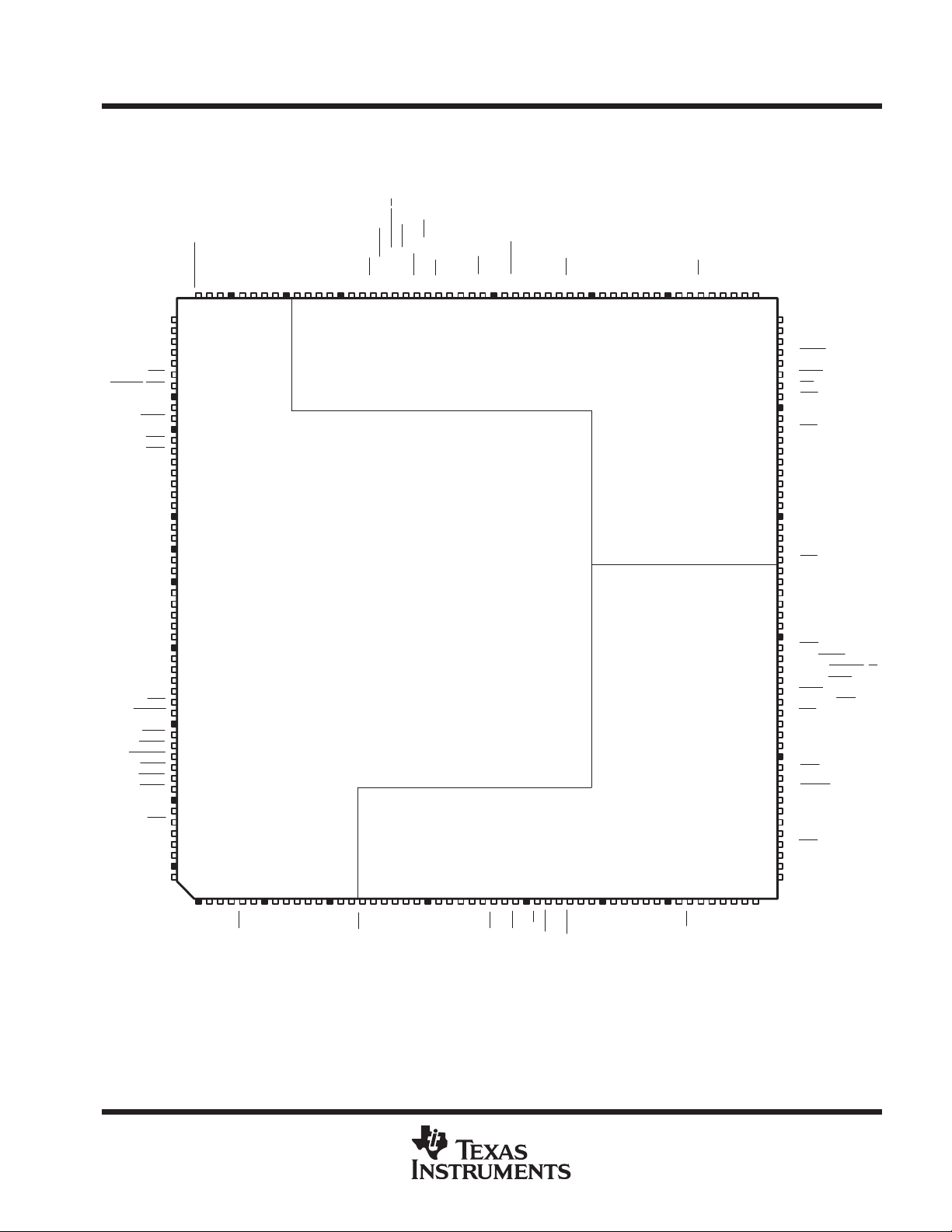
terminal assignments (continued)
PCI1221 GHK/PDV
PC CARD CONTROLLERS
SCPS042 – JULY 1998
PDV LOW-PROFILE QUAD FLAT PACKAGE
TOP VIEW
MFUNC2
MFUNC3
MFUNC4
MFUNC5
MFUNC6
C/BE3
RI_OUT/PME
V
CC
AD25
PRST
GND
GNT
REQ
AD31
AD30
AD11
AD29
AD28
V
CC
AD27
AD26
V
CCP
AD24
PCLK
GND
IDSEL
AD23
AD22
AD21
AD20
V
CC
AD19
AD18
AD17
AD16
C/BE2
FRAME
GND
IRDY
TRDY
DEVSEL
STOP
PERR
SERR
V
CC
PAR
C/BE1
AD15
AD14
AD13
GND
AD12
A_D10
A_D2
146
147
CC
V
A_D9
A_D8
A_D1
142
144
143
145
PCI1221 Core
A_BVD2(SPKR)
A_CD2
A_D0
A_WP(IOIS16)
A_BVD1(STSCHG/RI)
138
137
140
139
141
A_A1
A_READY(IREQ)
A_WAIT
A_A0
A_VS1
132
134
133
136
135
A_A2
131
A_REG
GND
130
129
Card A
A_A3
128
A_INPACK
127
A_A4
126
A_A5
125
CCI
DATA
152
LATCH
CLOCK
150
151
V
SPKROUT
148
149
SUSPEND
GND
MFUNC0
MFUNC1
154
153
156
155
157
158
159
160
161
162
163
164
165
166
167
168
169
170
171
172
173
174
175
176
177
178
179
180
181
182
183
184
185
186
187
188
189
190
191
192
193
194
195
196
197
198
199
200
201
202
203
204
205
206
207
208
214365871091211141316151817201922212423262528273029323134333635383740394241444346454847504952
A_A6
A_RESET
A_VS2
122
124
123
Card B
CCA
V
A_A25
120
121
A_A7
119
A_A24
118
A_A23
A_A12
116
117
A_A22
A_A15
114
115
CC
A_A16VA_A21
112
113
111
A_A20
A_WE
110
109
A_A19
A_A14
108
107
A_A18
A_A13
105
104
103
102
101
100
99
98
97
96
95
94
93
92
91
90
89
88
87
86
85
84
83
82
81
80
79
78
77
76
75
74
73
72
71
70
69
68
67
66
65
64
63
62
61
60
59
58
57
56
55
54
53
51 106
A_A8
A_A17
A_A9
A_IOWR
A_A11
A_IORD
A_OE
A_CE2
GND
A_A10
A_CE1
A_D15
A_D7
A_D14
A_D6
A_D13
A_D5
A_D12
V
CC
A_D4
A_D11
A_D3
A_CD1
B_D10
B_D2
B_D9
B_D1
B_D8
B_D0
GND
B_CD2
B_WP(IOIS16)
B_BVD1(STSCHG/RI)
B_BVD2(SPKR)
B_WAIT
B_READY(IREQ)
B_VS1
B_A0
B_A1
B_A2
V
CC
B_REG
B_A3
B_INPACK
B_A4
B_A5
B_RESET
B_A6
B_VS2
B_A25
B_A7
B_A24
CCP
V
AD9
AD10
AD8
AD7
C/BE0
CC
V
AD6
AD5
AD4
AD3
AD2
GND
AD1
AD0
B_D3
B_CD1
B_D11
B_D4
B_D5
B_D12
GND
B_D6
B_D13
B_D7
B_D14
B_D15
B_CE1
B_A10
B_CE2
V
CC
B_OE
B_IORD
B_A11
B_IOWR
B_A9
CCB
V
B_A17
B_A8
B_A18
B_A13
B_A19
GND
B_A14
B_WE
B_A20
B_A21
B_A16
B_A15
B_A22
B_A23
B_A12
PCI-to-PC Card (16-Bit) Diagram
POST OFFICE BOX 655303 • DALLAS, TEXAS 75265
5
Page 6
PCI1221 GHK/PDV
PC CARD CONTROLLERS
SCPS042 – JUL Y 1998
terminal assignments (continued)
GHK PLASTIC BALL GRID ARRAY
BOTTOM VIEW
signal names and terminal assignments
Table 1 and Table 2 show the terminal assignments for the CardBus PC Card; Table 3 and Table 4 show the
terminal assignments for the 16-bit PC Card; Table 1 and Table 3 show the CardBus PC Card and the 16-bit
PC Card terminals sorted alphanumerically by the associated GHK package terminal number; and Table 2 and
Table 4 show the CardBus PC Card and the 16-bit PC Card terminals sorted alphanumerically by the signal
name and it’s associated terminal numbers.
6
POST OFFICE BOX 655303 • DALLAS, TEXAS 75265
Page 7
SIGNAL NAME
SIGNAL NAME
SIGNAL NAME
SIGNAL NAME
PCI1221 GHK/PDV
PC CARD CONTROLLERS
SCPS042 – JULY 1998
Table 1. CardBus PC Card Signal Names by GHK/PDV Pin Number
PIN NO.
GHK PDV
D1 1 V
A4 208 AD12 F2 8 AD6 K14 132 A_CAD25 P5 50 B_CIRDY
E6 206 AD13 E7 201 V
C6 202 PAR C7 197 DEVSEL K17 130 A_CC/BE3 V5 57 B_CAD20
F7 198 STOP F8 193 FRAME L2 30 B_CAD10 V6 60 B_CAD22
E8 194 GND E9 189 AD18 L3 31 V
A8 190 AD17 A9 185 AD21 L6 32 B_CAD11 U8 68 B_CVS1
B9 186 AD20 B10 181 GND L1 29 B_CAD9 V9 72 B_CSTSCHG
C10 182 IDSEL C11 177 AD26 L17 125 A_CAD21 W10 76 B_CAD27
E11 178 V
A12 174 AD28 B13 169 REQ L14 127 A_CREQ P11 84 A_CAD2
A13 170 AD31 E13 165 AD25 L15 126 A_CAD22 U12 88 A_CAD3
A14 166 PRST G15 149 SPKROUT M1 34 B_CAD12 V13 92 A_CAD7
A15 162 C/BE3 F14 152 DATA M2 35 B_CAD15 V14 96 GND
E14 159 MFUNC4 E19 151 CLOCK M3 36 B_CAD14 P14 100 A_CAD12
C15 158 MFUNC3 F17 150 LATCH L5 33 B_CAD13 R18 109 A_CSTOP
A16 157 MFUNC2 F1 10 AD4 M18 121 A_CAD19 N14 108 A_CPERR
E3 2 AD10 H6 11 AD3 L18 124 A_CRST P15 107 A_CBLOCK
C5 207 GND G3 12 AD2 L19 123 A_CAD20 T1 52 B_CC/BE2
B5 205 AD14 G5 9 AD5 M19 122 A_CVS2 R3 51 B_CFRAME
A5 203 C/BE1 G17 145 A_CAD30 M5 38 V
A6 199 PERR F18 148 V
A7 195 IRDY F19 147 A_CAD31 N2 40 B_RSVD P8 63 B_CC/BE3
B8 191 AD16 G14 146 A_RSVD M6 37 B_CAD16 R8 67 B_CAD26
C9 187 V
E10 183 AD23 H5 15 AD0 M17 120 V
F11 179 AD24 H3 16 B_CCD1 M15 119 A_CAD18 R10 79 B_CAD30
A11 175 V
E12 171 AD30 H14 141 A_CAD27 N6 42 B_CBLOCK V12 87 A_CAD4
F12 167 GND G18 144 A_CAD29 P1 43 B_CPERR W13 91 A_RSVD
C14 163 RI_OUT/PME G19 143 V
F13 160 MFUNC5 H15 142 A_CAD28 N3 41 B_CPAR W15 99 A_CAD13
E17 155 MFUNC1 H1 18 B_CAD2 N15 113 V
D19 156 SUSPEND J1 19 B_CAD1 N17 116 A_CFRAME U15 103 A_CAD16
F5 3 AD9 J2 20 B_CAD4 M14 115 A_CIRDY R17 106 A_CPAR
G6 4 AD8 H2 17 B_CAD0 P19 114 A_CTRDY W4 53 B_CAD17
E2 5 C/BE0 J15 137 A_CAUDIO P3 46 B_CGNT U5 54 B_CAD18
F6 204 AD15 H17 140 A_CCD2 R1 47 B_CDEVSEL R6 55 B_CAD19
B6 200 SERR H18 139 A_CCLKRUN P6 48 B_CCLK W5 58 B_CRST
B7 196 TRDY H19 138 A_CSTSCHG N5 45 B_CSTOP W6 62 B_CAD23
C8 192 C/BE2 J5 22 GND R7 61 B_CREQ W7 66 B_CAD25
F9 188 AD19 J6 23 B_CAD6 V7 65 B_CAD24 W8 70 B_CSERR
F10 184 AD22 K1 24 B_CAD5 V8 69 B_CINT R9 74 B_CCD2
A10 180 PCLK J3 21 B_CAD3 U9 73 B_CCLKRUN U10 78 B_CAD29
B11 176 AD27 J19 133 A_CAD26 V10 77 B_CAD28 V11 82 A_CCD1
C12 172 AD11 J14 136 A_CSERR W11 81 B_CAD31 W12 86 V
C13 168 GNT J17 135 A_CINT R11 85 A_CAD1 R12 90 A_CAD5
B14 164 V
B15 161 MFUNC6/CLKRUN K3 26 B_CAD7 U13 93 A_CAD8 U14 98 A_CAD11
E18 153 GND K5 27 B_CAD8 R13 97 A_CAD10 R14 102 A_CAD14
F15 154 MFUNC0 K6 28 B_CC/BE0 P18 112 A_CCLK W16 104 A_CC/BE1
E1 6 AD7 K2 25 B_RSVD P17 111 A_CDEVSEL T19 105 A_RSVD
CCP
CCP
CC
CC
CC
PIN NO.
GHK PDV
F3 7 V
B12 173 AD29 K19 128 A_CAD23 P10 80 B_RSVD
G1 14 AD1 N18 117 A_CC/BE2 W9 71 B_CAUDIO
G2 13 GND N19 118 A_CAD17 U11 83 A_CAD0
J18 134 A_CVS1 P12 89 A_CAD6 P13 94 A_CC/BE0
CC
CC
CCI
CC
PIN NO.
GHK PDV
K18 129 GND R19 110 A_CGNT
K15 131 A_CAD24 R2 49 B_CTRDY
CC
CCB
N1 39 B_CC/BE1 U6 59 B_CAD21
CCA
P2 44 GND W14 95 A_CAD9
CC
PIN NO.
GHK PDV
U7 64 V
P7 56 B_CVS2
P9 75 GND
V15 101 A_CAD15
CC
CC
POST OFFICE BOX 655303 • DALLAS, TEXAS 75265
7
Page 8
PCI1221 GHK/PDV
SIGNAL NAME
SIGNAL NAME
SIGNAL NAME
SIGNAL NAME
PC CARD CONTROLLERS
SCPS042 – JUL Y 1998
Table 2. CardBus PC Card Signal Names Sorted Alphabetically
PIN NO.
GHK PDV
A_CAD0 U11 83 A_CSTOP R18 109 B_CAD12 M1 34 CLOCK E19 151
A_CAD1 R11 85 A_CSTSCHG H19 138 B_CAD13 L5 33 DATA F14 152
A_CAD2 P11 84 A_CTRDY P19 114 B_CAD14 M3 36 DEVSEL C7 197
A_CAD3 U12 88 A_CVS1 J18 134 B_CAD15 M2 35 FRAME F8 193
A_CAD4 V12 87 A_CVS2 M19 122 B_CAD16 M6 37 GND E8 194
A_CAD5 R12 90 A_RSVD G14 146 B_CAD17 W4 53 GND C5 207
A_CAD6 P12 89 A_RSVD W13 91 B_CAD18 U5 54 GND F12 167
A_CAD7 V13 92 A_RSVD T19 105 B_CAD19 R6 55 GND E18 153
A_CAD8 U13 93 AD0 H5 15 B_CAD20 V5 57 GND B10 181
A_CAD9 W14 95 AD1 G1 14 B_CAD21 U6 59 GND G2 13
A_CAD10 R13 97 AD2 G3 12 B_CAD22 V6 60 GND J5 22
A_CAD11 U14 98 AD3 H6 11 B_CAD23 W6 62 GND K18 129
A_CAD12 P14 100 AD4 F1 10 B_CAD24 V7 65 GND P2 44
A_CAD13 W15 99 AD5 G5 9 B_CAD25 W7 66 GND V14 96
A_CAD14 R14 102 AD6 F2 8 B_CAD26 R8 67 GND P9 75
A_CAD15 V15 101 AD7 E1 6 B_CAD27 W10 76 GNT C13 168
A_CAD16 U15 103 AD8 G6 4 B_CAD28 V10 77 IDSEL C10 182
A_CAD17 N19 118 AD9 F5 3 B_CAD29 U10 78 IRDY A7 195
A_CAD18 M15 119 AD10 E3 2 B_CAD30 R10 79 LATCH F17 150
A_CAD19 M18 121 AD11 C12 172 B_CAD31 W11 81 MFUNC0 F15 154
A_CAD20 L19 123 AD12 A4 208 B_CAUDIO W9 71 MFUNC1 E17 155
A_CAD21 L17 125 AD13 E6 206 B_CBLOCK N6 42 MFUNC2 A16 157
A_CAD22 L15 126 AD14 B5 205 B_CC/BE0 K6 28 MFUNC3 C15 158
A_CAD23 K19 128 AD15 F6 204 B_CC/BE1 N1 39 MFUNC4 E14 159
A_CAD24 K15 131 AD16 B8 191 B_CC/BE2 T1 52 MFUNC5 F13 160
A_CAD25 K14 132 AD17 A8 190 B_CC/BE3 P8 63 MFUNC6/CLKRUN B15 161
A_CAD26 J19 133 AD18 E9 189 B_CCD1 H3 16 PAR C6 202
A_CAD27 H14 141 AD19 F9 188 B_CCD2 R9 74 PCLK A10 180
A_CAD28 H15 142 AD20 B9 186 B_CCLK P6 48 PERR A6 199
A_CAD29 G18 144 AD21 A9 185 B_CCLKRUN U9 73 PRST A14 166
A_CAD30 G17 145 AD22 F10 184 B_CDEVSEL R1 47 REQ B13 169
A_CAD31 F19 147 AD23 E10 183 B_CFRAME R3 51 RI_OUT/PME C14 163
A_CAUDIO J15 137 AD24 F11 179 B_CGNT P3 46 SERR B6 200
A_CBLOCK P15 107 AD25 E13 165 B_CINT V8 69 SPKROUT G15 149
A_CC/BE0 P13 94 AD26 C11 177 B_CIRDY P5 50 STOP F7 198
A_CC/BE1 W16 104 AD27 B11 176 B_CPAR N3 41 SUSPEND D19 156
A_CC/BE2 N18 117 AD28 A12 174 B_CPERR P1 43 TRDY B7 196
A_CC/BE3 K17 130 AD29 B12 173 B_CREQ R7 61 V
A_CCD1 V11 82 AD30 E12 171 B_CRST W5 58 V
A_CCD2 H17 140 AD31 A13 170 B_CSERR W8 70 V
A_CCLK P18 112 B_CAD0 H2 17 B_CSTOP N5 45 V
A_CCLKRUN H18 139 B_CAD1 J1 19 B_CSTSCHG V9 72 V
A_CDEVSEL P17 111 B_CAD2 H1 18 B_CTRDY R2 49 V
A_CFRAME N17 116 B_CAD3 J3 21 B_CVS1 U8 68 V
A_CGNT R19 110 B_CAD4 J2 20 B_CVS2 P7 56 V
A_CINT J17 135 B_CAD5 K1 24 B_RSVD K2 25 V
A_CIRDY M14 115 B_CAD6 J6 23 B_RSVD N2 40 V
A_CPAR R17 106 B_CAD7 K3 26 B_RSVD P10 80 V
A_CPERR N14 108 B_CAD8 K5 27 C/BE0 E2 5 V
A_CREQ L14 127 B_CAD9 L1 29 C/BE1 A5 203 V
A_CRST L18 124 B_CAD10 L2 30 C/BE2 C8 192 V
A_CSERR J14 136 B_CAD11 L6 32 C/BE3 A15 162 V
PIN NO.
GHK PDV
PIN NO.
GHK PDV
CC
CC
CC
CC
CC
CC
CC
CC
CC
CC
CCA
CCB
CCI
CCP
CCP
PIN NO.
GHK PDV
C9 187
A11 175
B14 164
F3 7
E7 201
G19 143
L3 31
N15 113
U7 64
W12 86
M17 120
M5 38
F18 148
D1 1
E11 178
8
POST OFFICE BOX 655303 • DALLAS, TEXAS 75265
Page 9
SIGNAL NAME
SIGNAL NAME
SIGNAL NAME
PCI1221 GHK/PDV
PC CARD CONTROLLERS
Table 3. 16-Bit PC Card Signal Names by GHK/PDV Pin Number
PIN NO.
GHK PDV
D1 1 V
A4 208 AD12 F2 8 AD6 K14 132 A_A1
E6 206 AD13 E7 201 V
C6 202 PAR C7 197 DEVSEL K17 130 A_REG
F7 198 STOP F8 193 FRAME L2
E8 194 GND E9 189 AD18 L3
A8 190 AD17 A9 185 AD21 L6
B9 186 AD20 B10 181 GND L1
C10 182 IDSEL C11 177 AD26 L17 125 A_A5
E11 178 V
A12 174 AD28 B13 169 REQ L14 127 A_INPACK
A13 170 AD31 E13 165 AD25 L15 126 A_A4
A14 166 PRST G15 149 SPKROUT M1
A15 162 C/BE3 F14 152 DATA M2
E14 159 MFUNC4 E19 151 CLOCK M3
C15 158 MFUNC3 F17 150 LATCH L5
A16 157 MFUNC2 F1 10 AD4 M18 121 A_A25
E3 2 AD10 H6 11 AD3 L18 124 A_RESET
C5 207 GND G3 12 AD2 L19 123 A_A6
B5 205 AD14 G5 9 AD5 M19 122 A_VS2
A5 203 C/BE1 G17 145 A_D9 M5
A6 199 PERR F18 148 V
A7 195 IRDY F19 147 A_D10 N2
B8 191 AD16 G14 146 A_D2 M6
C9 187 V
E10 183 AD23 H5 15 AD0 M17 120 V
F11 179 AD24 H3 16 B_CD1 M15 119 A_A7
A11 175 V
E12 171 AD30 H14 141 A_D0 N6
F12 167 GND G18 144 A_D1 P1
C14 163 RI_OUT/PME G19 143 V
F13 160 MFUNC5 H15 142 A_D8 N3
E17 155 MFUNC1 H1 18 B_D11 N15 113 V
D19 156 SUSPEND J1
F5 3 AD9 J2
G6 4 AD8 H2 17 B_D3 P19 114 A_A22
E2 5 C/BE0 J15 137 A_BVD2(SPKR)P3
F6 204 AD15 H17 140 A_CD2 R1
B6 200 SERR H18 139 A_WP(IOIS16)P6
B7 196 TRDY H19 138 A_BVD1(STSCHG/RI)N545B_A20
C8 192 C/BE2 J5
F9 188 AD19 J6
F10 184 AD22 K1
A10 180 PCLK J3 21 B_D5 U9
B11 176 AD27 J19 133 A_A0 V10
C12 172 AD11 J14 136 A_WAIT W11
C13 168 GNT J17 135 A_READY(IREQ)R1185A_D4
B14 164 V
B15 161 MFUNC6 K3
E18 153 GND K5
F15 154 MFUNC0 K6
E1 6 AD7 K2
CCP
CCP
CC
CC
CC
PIN NO.
GHK PDV
F3 7 V
B12 173 AD29 K19 128 A_A3
G1 14 AD1 N18 117 A_A12
G2 13 GND N19 118 A_A24
J18 134 A_VS1 P12
CC
CC
CCI
CC
B_D4 N17 116 A_A23
19
B_D12 M14 115 A_A15
20
GND R7
22
B_D13 V7
23
B_D6 V8
24
B_D7 U13
26
B_D15 R13
27
B_CE1 P18 112 A_A16
28
B_D14 P17 111 A_A21
25
PIN NO.
GHK PDV
K18 129 GND
K15 131 A_A2
B_CE2
30
V
31
CC
B_OE
32
B_A10
29
B_A11
34
B_IOWR
35
B_A9
36
B_IORD
33
V
38
N1
P2
B_A8
39
B_A18
40
B_A17
37
B_A19
42
B_A14
43
GND
44
B_A13
41
B_WE
46
B_A21
47
B_A16
48
B_INPACK
61
B_A2
65
B_READY(IREQ)
69
B_WP(IOIS16)
73
B_D8
77
B_D10
81
A_D13
89
A_D15
93
A_CE2
97
CCB
CCA
CC
SCPS042 – JULY 1998
POST OFFICE BOX 655303 • DALLAS, TEXAS 75265
9
Page 10
PCI1221 GHK/PDV
SIGNAL NAME
SIGNAL NAME
SIGNAL NAME
SIGNAL NAME
SIGNAL NAME
SIGNAL NAME
PC CARD CONTROLLERS
SCPS042 – JUL Y 1998
Table 3. 16-Bit PC Card Signal Names by GHK/PDV Pin Number (Continued)
PIN NO.
GHK PDV
R19 110 A_WE T1
P5
R2
V5
V6
U7
U8
V9
W10
P10
P11
U12
V13
V14
P14
R18 109 A_A20 U15
N14 108 A_A14 R17 106 A_A13
P15 107 A_A19 W4
B_A15 R3
50
B_A22 P7
49
B_A6 U6
57
B_A4 P8
60
V
64
CC
B_VS1 W9
68
72 B_BVD1(STSCHG/RI)
B_D0 R10
76
B_D2 U11
80
A_D11 V12
84
A_D5 W13
88
A_D7 W14
92
GND W15
96
A_A11 V15
100
PIN NO.
GHK PDV
52
51
56
59
63
R8
67
71
P9
75
79
83
87
91
95
99
101
103
53
PIN NO.
GHK PDV
B_A12 U5
B_A23 R6
B_VS2 W5
B_A5 W6
B_REG W7
B_A0 W8
B_BVD2(SPKR)R974B_CD2
GND U10
B_D9 V11
A_D3 W12
A_D12 R12
A_D14 P13
A_A10 U14
A_IORD R14
A_IOWR W16
A_A17 T19 105 A_A18
B_A24
54
55
58
62
66
70
78
82
86
90
94
98
102
104
B_A7
B_A25
B_RESET
B_A3
B_A1
B_WAIT
B_D1
A_CD1
V
CC
A_D6
A_CE1
A_OE
A_A9
A_A8
Table 4. 16-Bit PC Card Signal Names Sorted Alphabetically
PIN NO.
GHK PDV
A_A0 J19 133 A_A20 R18 109 A_D8 H15 142
A_A1 K14 132 A_A21 P17 111 A_D9 G17 145
A_A2 K15 131 A_A22 P19 114 A_D10 F19 147
A_A3 K19 128 A_A23 N17 116 A_D11 P11
A_A4 L15 126 A_A24 N19 118 A_D12 V12
A_A5 L17 125 A_A25 M18 121 A_D13 P12
A_A6 L19 123 A_BVD1(STSCHG/RI) H19 138 A_D14 W13
A_A7 M15 119 A_BVD2(SPKR) J15 137 A_D15 U13
A_A8 W16
A_A9 R14
A_A10 W14
A_A11 P14
A_A12 N18 117 A_D0 H14 141 A_READY(IREQ) J17 135
A_A13 R17 106 A_D1 G18 144 A_REG K17 130
A_A14 N14 108 A_D2 G14 146 A_RESET L18 124
A_A15 M14 115 A_D3 U11
A_A16 P18 112 A_D4 R11
A_A17 U15
A_A18 T19 105 A_D6 R12
A_A19 P15 107 A_D7 V13
A_CD1 V11
104
A_CD2 H17 140 A_IORD W15
102
A_CE1 P13
95
A_CE2 R13
100
A_D5 U12
103
PIN NO.
GHK PDV
82
94
97
83
85
88
90
92
PIN NO.
GHK PDV
84
87
89
91
93
A_INPACK L14 127
99
A_IOWR V15
A_OE U14
A_VS1 J18 134
A_VS2 M19 122
A_WAIT J14 136
A_WE R19 110
A_WP(IOIS16) H18 139
101
98
10
POST OFFICE BOX 655303 • DALLAS, TEXAS 75265
Page 11
SIGNAL NAME
SIGNAL NAME
SIGNAL NAME
PCI1221 GHK/PDV
PC CARD CONTROLLERS
SCPS042 – JULY 1998
Table 4. 16-Bit PC Card Signal Names Sorted Alphabetically (Continued)
PIN NO.
GHK PDV
AD0 H5 15 B_A18 N2
AD1 G1 14 B_A19 N6
AD2 G3 12 B_A20 N5
AD3 H6 11 B_A21 R1
AD4 F1 10 B_A22 R2
AD5 G5 9 B_A23 R3
AD6 F2 8 B_A24 W4
AD7 E1 6 B_A25 R6
AD8 G6 4
AD9 F5 3 B_BVD2(SPKR) W9
AD10 E3 2 B_CD1 H3 16 GND P9
AD11 C12 172 B_CD2 R9
AD12 A4 208 B_CE1 K6
AD13 E6 206 B_CE2 L2
AD14 B5 205 B_D0 W10
AD15 F6 204 B_D1 U10
AD16 B8 191 B_D2 P10
AD17 A8 190 B_D3 H2 17 MFUNC2 A16 157
AD18 E9 189 B_D4 J1
AD19 F9 188 B_D5 J3 21 MFUNC4 E14 159
AD20 B9 186 B_D6 K1
AD21 A9 185 B_D7 K3
AD22 F10 184 B_D8 V10
AD23 E10 183 B_D9 R10
AD24 F11 179 B_D10 W11
AD25 E13 165 B_D11 H1 18 PRST A14 166
AD26 C11 177 B_D12 J2
AD27 B11 176 B_D13 J6
AD28 A12 174 B_D14 K2
AD29 B12 173 B_D15 K5
AD30 E12 171 B_INPACK R7
AD31 A13 170 B_IORD L5
B_A0 R8
B_A1 W7
B_A2 V7
B_A3 W6
B_A4 V6
B_A5 U6
B_A6 V5
B_A7 U5
B_A8 N1
B_A9 M3
B_A10 L1
B_A11 M1
B_A12 T1
B_A13 N3
B_A14 P1
B_A15 P5
B_A16 P6
B_A17 M6
B_BVD1(STSCHG/RI)
B_IOWR M2
67
B_OE L6
66
B_READY(IREQ) V8
65
B_REG P8
62
B_RESET W5
60
B_VS1 U8
59
B_VS2 P7
57
B_WAIT W8
54
B_WE P3
39
B_WP(IOIS16) U9
36
C/BE0 E2 5 V
29
C/BE1 A5 203 V
34
C/BE2 C8 192 V
52
C/BE3 A15 162 V
41
CLOCK E19 151 V
43
DATA F14 152 V
50
DEVSEL C7 197
48
FRAME F8 193
37
PIN NO.
GHK PDV
40
42
45
47
49
51
53
55
V9
72
71
74
28
30
76
78
80
19
24
26
77
79
81
20
23
25
27
61
33
35
32
69
63
58
68
56
70
46
73
PIN NO.
GHK PDV
GND E8 194
GND C5 207
GND F12 167
GND E18 153
GND B10 181
GND G2 13
GND J5
GND K18 129
GND P2
GND V14
22
44
96
75
GNT C13 168
IDSEL C10 182
IRDY A7 195
LATCH F17 150
MFUNC0 F15 154
MFUNC1 E17 155
MFUNC3 C15 158
MFUNC5 F13 160
MFUNC6 B15 161
PAR C6 202
PCLK A10 180
PERR A6 199
REQ B13 169
RI_OUT/PME C14 163
SERR B6 200
SPKROUT G15 149
STOP F7 198
SUSPEND D19 156
TRDY B7 196
V
CC
V
CC
V
CC
V
CC
V
CC
V
CC
V
CC
V
CC
V
CC
CC
CCA
CCB
CCI
CCP
CCP
A11 175
C9 187
B14 164
F3 7
E7 201
G19 143
L3
N15 113
U7
W12
M17 120
M5
F18 148
D1 1
E11 178
31
64
86
38
POST OFFICE BOX 655303 • DALLAS, TEXAS 75265
11
Page 12
PCI1221 GHK/PDV
FUNCTION
I/O
NAME
TYPE
NAME
TYPE
PC CARD CONTROLLERS
SCPS042 – JUL Y 1998
Terminal Functions
The terminals are grouped in tables by functionality, such as PCI system function, power-supply function, etc. The
terminal numbers are also listed for convenient reference.
power supply
TERMINAL
NAME PDV NUMBER GHK NUMBER
GND
V
CC
V
CCA
V
CCB
V
CCI
V
CCP
13, 22, 44, 75, 96, 129, 153,
167, 181, 194, 207
7, 31, 64, 86, 113, 143, 164,
175, 187, 201
120 M17
38 M5
148 F18
1, 178 D1, E11 Clamp voltage for PCI signaling (5 V or 3.3 V)
G2, J5, P2, P9, V14, K18, E18,
F12, B10, E8, C5
F3, L3, U7, W12, N15, G19,
B14, A11, C9, E7
Device ground terminals
Power supply terminal for core logic (3.3 V)
Clamp voltage for PC Card A interface. Indicates Card A
signaling environment, 5 V or 3.3 V.
Clamp voltage for PC Card B interface. Indicates Card B
signaling environment, 5 V or 3.3 V.
Clamp voltage for interrupt subsystem interface and
miscellaneous I/O. (5 V or 3.3 V)
PC Card power switch
TERMINAL
PIN NUMBER
PDV GHK
CLOCK 151 E19 I/O
DATA 152 F14 O
LATCH 150 F17 O
PCI system
TERMINAL
PIN NUMBER
PDV GHK
PCLK 180 A10 I
PRST
166 A14 I
FUNCTION
Three-line power switch clock. Information on the DATA line is sampled at the rising edge of CLOCK.
CLOCK defaults to an input, but can be changed to a PCI1221 output by using the P2CCLK bit in the
System Control Register. The TPS2206 defines the maximum frequency of this signal to be 2 MHz.
If a system design defines this terminal as an output, then this terminal requires an external pull down
resister. The frequency of the PCI1221 output CLOCK is derived from dividing the PCI CLK by 36.
Three-line power switch data. DATA is used to serially communicate socket power control information
to the power switch.
Three-line power switch latch. LATCH is asserted by the PCI1221 to indicate to the PC Card power
switch that the data on the DATA line is valid. When a pulldown resistor is implemented on this
terminal, the MFUNC4 and MFUNC1 terminals provide the serial EEPROM SCL and SDA interface.
I/O
PCI bus clock. PCLK provides timing for all transactions on the PCI bus. All PCI signals are sampled at
the rising edge of PCLK.
PCI reset. When the PCI bus reset is asserted, PRST causes the PCI1221 to place all output buffers
in a high-impedance state and reset all internal registers. When PRST
completely nonfunctional. After PRST
When the SUSPEND and PRST are asserted, the device is protected from the PRST clearing the internal
registers. All outputs are placed in a high-impedance state, but the contents of the registers are
preserved.
FUNCTION
is asserted, the device is
is deasserted, the PCI1221 is in its default state.
12
POST OFFICE BOX 655303 • DALLAS, TEXAS 75265
Page 13
NAME
TYPE
PCI address and data
TERMINAL
PIN NUMBER
PDV GHK
AD31
AD30
AD29
AD28
AD27
AD26
AD25
AD24
AD23
AD22
AD21
AD20
AD19
AD18
AD17
AD16
AD15
AD14
AD13
AD12
AD11
AD10
AD9
AD8
AD7
AD6
AD5
AD4
AD3
AD2
AD1
AD0
C/BE3
C/BE2
C/BE1
C/BE0
PAR 202 C6 I/O
170
171
173
174
176
177
165
179
183
184
185
186
188
189
190
191
204
205
206
208
172
2
3
4
6
8
9
10
11
12
14
15
162
192
203
5
A13
E12
B12
A12
B11
C11
E13
F11
E10
F10
A9
B9
F9
E9
A8
B8
F6
B5
E6
A4
C12
E3
F5
G6
E1
F2
G5
F1
H6
G3
G1
H5
A15
C8
A5
E2
PCI1221 GHK/PDV
PC CARD CONTROLLERS
SCPS042 – JULY 1998
Terminal Functions (Continued)
I/O
PCI address/data bus. These signals make up the multiplexed PCI address and data bus on the primary
interface. During the address phase of a primary bus PCI cycle, AD31-AD0 contain a 32-bit address or
I/O
other destination information. During the data phase, AD31-AD0 contain data.
PCI bus commands and byte enables. These signals are multiplexed on the same PCI terminals. During
the address phase of a primary bus PCI cycle, C/BE3
phase, this 4-bit bus is used as byte enables. The byte enables determine which byte paths of the full 32-bit
I/O
data bus carry meaningful data. C/BE0
(AD15–AD8), C/BE2
PCI bus parity. In all PCI bus read and write cycles, the PCI1221 calculates even parity across the
AD31–AD0 and C/BE3–
indicator with a one-PCLK delay. As a target during PCI cycles, the calculated parity is compared to the
initiator’s parity indicator. A compare error results in the assertion of a parity error (PERR
applies to byte 2 (AD23–AD16), and C/BE3 applies to byte 3 (AD31–AD24).
C/BE0 buses. As an initiator during PCI cycles, the PCI1221 outputs this parity
FUNCTION
–C/BE0 define the bus command. During the data
applies to byte 0 (AD7–AD0), C/BE1 applies to byte 1
).
POST OFFICE BOX 655303 • DALLAS, TEXAS 75265
13
Page 14
PCI1221 GHK/PDV
NAME
TYPE
PC CARD CONTROLLERS
SCPS042 – JUL Y 1998
PCI interface control
TERMINAL
PIN NUMBER
PDV GHK
DEVSEL
FRAME
GNT
IDSEL 182 C10 I
IRDY
PERR
REQ
SERR
STOP
TRDY
197 C7 I/O
193 F8 I/O
168 C13 I
195 A7 I/O
199 A6 I/O
169 B13 O PCI bus request. REQ is asserted by the PCI1221 to request access to the PCI bus as an initiator.
200 B6 O
198 F7 I/O
196 B7 I/O
I/O
Terminal Functions (Continued)
FUNCTION
PCI device select. The PCI1221 asserts DEVSEL to claim a PCI cycle as the target device. As a
PCI initiator on the bus, the PCI1221 monitors DEVSEL
responds before timeout occurs, the PCI1221 terminates the cycle with an initiator abort.
PCI cycle frame. FRAME is driven by the initiator of a bus cycle. FRAME is asserted to indicate that
a bus transaction is beginning, and data transfers continue while this signal is asserted. When
is deasserted, the PCI bus transaction is in the final data phase.
FRAME
PCI bus grant. GNT is driven by the PCI bus arbiter to grant the PCI1221 access to the PCI bus
after the current data transaction has completed. GNT
depending on the PCI bus parking algorithm.
Initialization device select. IDSEL selects the PCI1221 during configuration space accesses.
IDSEL can be connected to one of the upper 24 PCI address lines on the PCI bus.
PCI initiator ready. IRDY indicates the PCI bus initiator’s ability to complete the current data phase
of the transaction. A data phase is completed on a rising edge of PCLK where both IRDY
are asserted. Until IRDY and TRDY are both sampled asserted, wait states are inserted.
PCI parity error indicator. PERR is driven by a PCI device to indicate that calculated parity does
not match PAR when PERR
PCI system error. SERR is an output that is pulsed from the PCI1221 when enabled through the
command register indicating a system error has occurred. The PCI1221 need not be the target of
the PCI cycle to assert this signal. When SERR
pulses, indicating that an address parity error has occurred on a CardBus interface.
PCI cycle stop signal. STOP is driven by a PCI target to request the initiator to stop the current PCI
bus transaction. STOP
that do not support burst data transfers.
PCI target ready. TRDY indicates the primary bus target’s ability to complete the current data phase
of the transaction. A data phase is completed on a rising edge of PCLK when both IRDY
are asserted. Until both IRDY and TRDY are asserted, wait states are inserted.
is enabled through bit 6 of the command register.
is enabled in the control register, this signal also
is used for target disconnects and is commonly asserted by target devices
until a target responds. If no target
may or may not follow a PCI bus request,
and TRDY
and TRDY
14
POST OFFICE BOX 655303 • DALLAS, TEXAS 75265
Page 15
I/O
NAME
TYPE
Terminal Functions (Continued)
multifunction and miscellaneous pins
TERMINAL
PIN NUMBER
PDV GHK
Multifunction terminal 0. MFUNC0 can be configured as parallel PCI interrupt INTA, GPI0,
MFUNC0 154 F15 I/O
MFUNC1 155 E17 I/O
MFUNC2 157 A16 I/O
MFUNC3 158 C15 I/O
GPO0, socket activity LED output, ZV switching outputs, CardBus audio PWM, GPE
parallel IRQ. Refer to the
configuration details.
Multifunction terminal 1. MFUNC1 can be configured as parallel PCI interrupt INTB, GPI1,
GPO1, socket activity LED output, ZV switching outputs, CardBus audio PWM, GPE
parallel IRQ. Refer to the
configuration details.
Serial data (SDA). When the serial bus mode is implemented by pulling the LATCH terminal
low, the MFUNC1 terminal provides the SDA signaling. The two pin serial interface is used to
load the subsystem identification and other register defaults from an EEPROM after a PCI
reset. Refer to the
other serial bus applications.
Multifunction terminal 2. MFUNC2 can be configured as GPI2, GPO2, socket activity LED
output, ZV switching outputs, CardBus audio PWM, GPE
multifunction routing register
Multifunction terminal 3. MFUNC3 can be configured as a parallel IRQ or the serialized
interrupt signal IRQSER. Refer to the
configuration details.
Multifunction terminal 4. MFUNC4 can be configured as PCI LOCK, GPI3, GPO3, socket
activity LED output, ZV switching outputs, CardBus audio PWM, GPE
to the
multifunction routing register
FUNCTION
multifunction routing register
multifunction routing register
serial bus interface implementation
description on page 62 for configuration details.
multifunction routing register
description on page 62 for configuration details.
PCI1221 GHK/PDV
PC CARD CONTROLLERS
SCPS042 – JULY 1998
, or a
description on page 62 for
, or a
description on page 62 for
description on page 29 for details on
, or a parallel IRQ. Refer to the
description on page 62 for
, or a parallel IRQ. Refer
MFUNC4 159 E14 I/O
MFUNC5 160 F13 I/O
MFUNC6 161 B15 I/O
RI_OUT/PME 163 C14 O
SPKROUT
SUSPEND 156 D19 I
149 G15 O
Serial clock (SCL). When the serial bus mode is implemented by pulling the LATCH terminal
low, the MFUNC4 terminal provides the SCL signaling. The two pin serial interface is used to
load the subsystem identification and other register defaults from an EEPROM after a PCI
reset. Refer to the
other serial bus applications.
Multifunction terminal 5. MFUNC5 can be configured as GPI4, GPO4, socket activity LED
output, ZV switching outputs, CardBus audio PWM, GPE
multifunction routing register
Multifunction terminal 6. MFUNC6 can be configured as a PCI CLKRUN or a parallel IRQ.
Refer to the
Ring Indicate Out and Power Management Event Output. Terminal provides an output for
ring-indicate or PME
Speaker output. SPKROUT is the output to the host system that can carry SPKR or CAUDIO
through the PCI1221 from the PC Card interface. SPKROUT is driven as the exclusive-OR
combination of card SPKR
Suspend. SUSPEND is used to protect the internal registers from clearing when the PRST
signal is asserted. See
serial bus interface implementation
description on page 62 for configuration details.
multifunction routing register
signals.
//CAUDIO inputs.
suspend mode
description on page 40 for details.
description on page 29 for details on
, or a parallel IRQ. Refer to the
description on page 62 for configuration details.
POST OFFICE BOX 655303 • DALLAS, TEXAS 75265
15
Page 16

PCI1221 GHK/PDV
FUNCTION
PC CARD CONTROLLERS
SCPS042 – JUL Y 1998
Terminal Functions (Continued)
16-bit PC Card address and data (slots A and B)
TERMINAL
PIN NUMBER
NAME
PDV
A25
A24
A23
A22
A21
A20
A19
A18
A17
A16
A15
A14
A13
A12
A11
A10
A9
A8
A7
A6
A5
A4
A3
A2
A1
A0
D15
D14
D13
D12
D11
D10
D9
D8
D7
D6
D5
D4
D3
D2
D1
D0
†
Terminal name for slot A is preceded with A_. For example, the full name for terminals 121 and M18 are A_A25.
‡
Terminal name for slot B is preceded with B_. For example, the full name for terminals 55 and R6 are B_A25.
121
118
116
114
111
109
107
105
103
112
115
108
106
117
100
95
102
104
119
123
125
126
128
131
132
133
93
91
89
87
84
147
145
142
92
90
88
85
83
146
144
141
SLOT A
†
GHK
M18
N19
N17
P19
P17
R18
P15
T19
U15
P18
M14
N14
R17
N18
P14
W14
R14
W16
M15
L19
L17
L15
K19
K15
K14
J19
U13
W13
P12
V12
P11
F19
G17
H15
V13
R12
U12
R11
U11
G14
G18
H14
SLOT B
PDV
55
53
51
49
47
45
42
40
37
48
50
43
41
52
34
29
36
39
54
57
59
60
62
65
66
67
27
25
23
20
18
81
79
77
26
24
21
19
17
80
78
76
GHK
R6
W4
R3
R2
R1
N5
N6
N2
M6
N3
M1
M3
N1
U5
U6
W6
W7
R8
H1
W11
R10
V10
H2
P10
U10
W10
I/O
‡
TYPE
P6
P5
P1
T1
L1
V5
V6
V7
K5
K2
J6
J2
K3
K1
J3
J1
O PC Card address. 16-bit PC Card address lines. A25 is the most-significant bit.
I/O PC Card data. 16-bit PC Card data lines. D15 is the most-significant bit.
16
POST OFFICE BOX 655303 • DALLAS, TEXAS 75265
Page 17
FUNCTION
PC CARD CONTROLLERS
Terminal Functions (Continued)
16-bit PC Card interface control (slots A and B)
TERMINAL
PIN NUMBER
NAME
PDV GHK PDV GHK
BVD1
(STSCHG
BVD2
(SPKR
)
CD1
CD2
CE1
CE2
INPACK 127 L14 61 R7 I
IORD
IOWR
OE 98 U14 32 L6 O
†
Terminal name for slot A is preceded with A_. For example, the full name for terminals 127 and L14 are A_INP ACK .
‡
Terminal name for slot B is preceded with B_. For example, the full name for terminals 61 and R7 are B_INPACK
138 H19 72 V9 I
/RI)
137 J15 71 W9 I
82
140
9497P13
99 W15 33 L5 O
101 V15 35 M2 O
†
SLOT A
V11
H171674H3R9
R132830
SLOT B
K6
L2
I/O
‡
TYPE
Battery voltage detect 1. BVD1 is generated by 16-bit memory PC Cards that
include batteries. BVD1 is used with BVD2 as an indication of the condition of the
batteries on a memory PC Card. Both BVD1 and BVD2 are kept high when the
battery is good. When BVD2 is low and BVD1 is high, the battery is weak and
should be replaced. When BVD1 is low, the battery is no longer serviceable and
the data in the memory PC Card is lost. See
configuration
register
status bits for this signal.
Status change. STSCHG
write protect, or battery voltage dead condition of a 16-bit I/O PC Card.
Ring indicate. RI
Battery voltage detect 2. BVD2 is generated by 16-bit memory PC Cards that
include batteries. BVD2 is used with BVD1 as an indication of the condition of the
batteries on a memory PC Card. Both BVD1 and BVD2 are high when the battery
is good. When BVD2 is low and BVD1 is high, the battery is weak and should be
replaced. When BVD1 is low, the battery is no longer serviceable and the data
in the memory PC Card is lost. See
configuration register
register
status bits for this signal.
Speaker. SPKR
and socket have been configured for the 16-bit I/O interface. The audio signals
from cards A and B are combined by the PCI1221 and are output on SPKROUT .
PC Card detect 1 and PC Card detect 2. CD1 and CD2 are internally connected
to ground on the PC Card. When a PC Card is inserted into a socket, CD1
I
CD2
Card enable 1 and card enable 2. CE1 and CE2 enable even- and odd-numbered
address bytes. CE1
O
odd-numbered address bytes.
Input acknowledge. INP ACK is asserted by the PC Card when it can respond to
an I/O read cycle at the current address.
I/O read. IORD is asserted by the PCI1221 to enable 16-bit I/O PC Card data
output during host I/O read cycles.
I/O write. IOWR is driven low by the PCI1221 to strobe write data into 16-bit I/O
PC Cards during host I/O write cycles.
Output enable. OE is driven low by the PCI1221 to enable 16-bit memory PC
Card data output during host memory read cycles.
register
on page 88 and the
on page 88 and the
are pulled low. For signal status, see
on page 89 for enable bits. See
ExCA interface status register
is used to alert the system to a change in the READY ,
is used by 16-bit modem cards to indicate a ring detection.
on page 89 for enable bits. See
ExCA interface status register
is an optional binary audio signal available only when the card
enables even-numbered address bytes, and CE2 enables
ExCA card status-change interrupt
ExCA card status-change interrupt
interface status register
PCI1221 GHK/PDV
SCPS042 – JULY 1998
ExCA card status-change
on page 85 for the
ExCA card status-change
on page 85 for the
and
on page 88.
.
POST OFFICE BOX 655303 • DALLAS, TEXAS 75265
17
Page 18
PCI1221 GHK/PDV
FUNCTION
PC CARD CONTROLLERS
SCPS042 – JUL Y 1998
Terminal Functions (Continued)
16-bit PC Card interface control (slots A and B) (continued)
TERMINAL
PIN NUMBER
NAME
PDV GHK PDV GHK
READY
(IREQ
)
REG
RESET 124 L18 58 W5 O PC Card reset. RESET forces a hard reset to a 16-bit PC Card.
WAIT
WE 110 R19 46 P3 O
WP
(IOIS16
)
VS1
VS2
†
Terminal name for slot A is preceded with A_. For example, the full name for terminals 1 10 and R19 are A_WE.
‡
Terminal name for slot B is preceded with B_. For example, the full name for terminals 46 and P3 are B_WE
135 J17 69 V8 I
130 K17 63 P8 O
136 J14 70 W8 I
139 H18 73 U9 I
134
122
†
SLOT A
J18
M196856U8P7
SLOT B
I/O
‡
TYPE
Ready. The ready function is provided by READY when the 16-bit PC Card and
the host socket are configured for the memory-only interface. READY is driven
low by the 16-bit memory PC Cards to indicate that the memory card circuits are
busy processing a previous write command. READY is driven high when the
16-bit memory PC Card is ready to accept a new data transfer command.
Interrupt request. IREQ
that a device on the 16-bit I /O PC Card requires service by the host software.
is high (deasserted) when no interrupt is requested.
IREQ
Attribute memory select. REG remains high for all common memory accesses.
When REG
and to the I/O space (IORD
accessed section of card memory and is generally used to record card capacity
and other configuration and attribute information.
Bus cycle wait. WAIT is driven by a 16-bit PC Card to delay the completion of (i.e.,
extend) the memory or I/O cycle in progress.
Write enable. WE is used to strobe memory write data into 16-bit memory PC
Cards. WE is also used for memory PC Cards that employ programmable
memory technologies.
Write protect. WP applies to 16-bit memory PC Cards. WP reflects the status of
the write-protect switch on 16-bit memory PC Cards. For 16-bit I/O cards, WP is
used for the 16-bit port (IOIS16
I/O is 16 bits. IOIS16
16-bit PC Card when the address on the bus corresponds to an address to which
the 16-bit PC Card responds, and the I/O port that is addressed is capable of
16-bit accesses.
Voltage sense 1 and voltage sense 2. VS1 and VS2, when used in conjunction
I/O
with each other, determine the operating voltage of the 16-bit PC Card.
is asserted, access is limited to attribute memory (OE or WE active)
is asserted by a 16-bit I/O PC Card to indicate to the host
or IOWR active). Attribute memory is a separately
) function.
applies to 16-bit I/O PC Cards. IOIS16 is asserted by the
.
18
POST OFFICE BOX 655303 • DALLAS, TEXAS 75265
Page 19
FUNCTION
PC CARD CONTROLLERS
Terminal Functions (Continued)
CardBus PC Card interface system (slots A and B)
TERMINAL
PIN NUMBER
NAME
PDV GHK PDV GHK
CCLK 112 P18 48 P6 O
CCLKRUN
CRST
†
Terminal name for slot A is preceded with A_. For example, the full name for terminals 1 12 and P18 are A_CCLK.
‡
Terminal name for slot B is preceded with B_. For example, the full name for terminals 48 and P6 are B_CCLK.
139 H18 73 U9 O
124 L18 58 W5 I/O
SLOT A
†
SLOT B
I/O
‡
TYPE
CardBus PC Card clock. CCLK provides synchronous timing for all transactions on
the CardBus interface. All signals except CRST
CAUDIO, CCD2-1
all timing parameters are defined with the rising edge of this signal. CCLK operates
at the PCI bus clock frequency, but it can be stopped in the low state or slowed down
for power savings.
CardBus PC Card clock run. CCLKRUN is used by a CardBus PC Card to request
an increase in the CCLK frequency, and by the PCI1221 to indicate that the CCLK
frequency is going to be decreased.
CardBus PC Card reset. CRST is used to bring CardBus PC Card-specific
registers, sequencers, and signals to a known state. When CRST
CardBus PC Card signals must be 3-stated, and the PCI1221 drives these signals
to a valid logic level. Assertion can be asynchronous to CCLK, but deassertion must
be synchronous to CCLK.
, and CVS2-CVS1 are sampled on the rising edge of CCLK, and
, CCLKRUN, CINT, CSTSCHG,
PCI1221 GHK/PDV
SCPS042 – JULY 1998
is asserted, all
POST OFFICE BOX 655303 • DALLAS, TEXAS 75265
19
Page 20
PCI1221 GHK/PDV
FUNCTION
PC CARD CONTROLLERS
SCPS042 – JUL Y 1998
Terminal Functions (Continued)
CardBus PC Card address and data (slots A and B)
TERMINAL
PIN NUMBER
NAME
PDV GHK PDV GHK
CAD31
CAD30
CAD29
CAD28
CAD27
CAD26
CAD25
CAD24
CAD23
CAD22
CAD21
CAD20
CAD19
CAD18
CAD17
CAD16
CAD15
CAD14
CAD13
CAD12
CAD11
CAD10
CAD9
CAD8
CAD7
CAD6
CAD5
CAD4
CAD3
CAD2
CAD1
CAD0
CC/BE3
CC/BE2
CC/BE1
CC/BE0
CPAR 106 R17 41 N3 I/O
†
Terminal name for slot A is preceded with A_. For example, the full name for terminals 106 and R17 are A_CP AR.
‡
Terminal name for slot B is preceded with B_. For example, the full name for terminals 41 and N3 are B_CPAR.
147
145
144
142
141
133
132
131
128
126
125
123
121
119
118
103
101
102
99
100
98
97
95
93
92
89
90
87
88
84
85
83
130
117
104
94
SLOT A
†
F19
G17
G18
H15
H14
J19
K14
K15
K19
L15
L17
L19
M18
M15
N19
U15
V15
R14
W15
P14
U14
R13
W14
U13
V13
P12
R12
V12
U12
P11
R11
U11
K17
N18
W16
P13
SLOT B
81
79
78
77
76
67
66
65
62
60
59
57
55
54
53
37
35
36
33
34
32
30
29
27
26
23
24
20
21
18
19
17
63
52
39
28
W11
R10
U10
V10
W10
W7
W6
W4
M6
M2
M3
M1
R8
V7
V6
U6
V5
R6
U5
L5
L6
L2
L1
K5
K3
J6
K1
J2
J3
H1
J1
H2
P8
T1
N1
K6
I/O
‡
TYPE
PC Card address and data. These signals make up the multiplexed CardBus address
and data bus on the CardBus interface. During the address phase of a CardBus cycle,
I/O
CAD31–CAD0 contain a 32-bit address. During the data phase of a CardBus cycle,
CAD31–CAD0 contain data. CAD31 is the most-significant bit.
CardBus bus commands and byte enables. CC/BE3–CC/BE0 are multiplexed on the
same CardBus terminals. During the address phase of a CardBus cycle,
CC/BE3–
used as byte enables. The byte enables determine which byte paths of the full 32-bit
I/O
data bus carry meaningful data. CC/BE0
applies to byte 1 (CAD15-CAD8), CC/BE2 applies to byte 2 (CAD23-CAD8), and
CC/BE3
CardBus parity. In all CardBus read and write cycles, the PCI1221 calculates even
parity across the CAD and CC/BE
PCI1221 outputs CPAR with a one-CCLK delay. As a target during CardBus cycles,
the calculated parity is compared to the initiator’s parity indicator; a compare error
results in a parity error assertion.
CC/BE0 defines the bus command. During the data phase, this 4-bit bus is
applies to byte 0 (CAD7-CAD0), CC/BE1
applies to byte 3 (CAD31-CAD24).
buses. As an initiator during CardBus cycles, the
20
POST OFFICE BOX 655303 • DALLAS, TEXAS 75265
Page 21
FUNCTION
I
ith CVS1
CVS2 to identif
I/O
i
ith CCD1
CCD2 to identif
PC CARD CONTROLLERS
Terminal Functions (Continued)
CardBus PC Card interface control (slots A and B)
TERMINAL
PIN NUMBER
NAME
PDV GHK PDV GHK
CAUDIO 137 J15 71 W9 I
CBLOCK
CCD1
CCD2
CDEVSEL
CFRAME
CGNT
CINT
CIRDY
CPERR
CREQ
CSERR
CSTOP
CSTSCHG
CTRDY
CVS1 134 J18 68 U8
CVS2 122 M19 56 P7
†
Terminal name for slot A is preceded with A_. For example, the full name for terminals 137 and J15 are A_CAUDIO.
‡
Terminal name for slot B is preceded with B_. For example, the full name for terminals 71 and W9 are B_CAUDIO.
107 P15 42 N6 I/O
82 V11 16 H3
140 H17 74 R9
111 P17 47 R1 I/O
116 N17 51 R3 I/O
110 R19 46 P3 I
135 J17 69 V8 I
115 M14 50 P5 I/O
108 N14 43 P1 I/O
127 L14 61 R7 I
136 J14 70 W8 I
109 R18 45 N5 I/O
138 H19 72 V9 I
114 P19 49 R2 I/O
SLOT A
†
SLOT B
I/O
‡
TYPE
CardBus audio. CAUDIO is a digital input signal from a PC Card to the system
speaker. The PCI1221 supports the binary audio mode and outputs a binary signal
from the card to SPKROUT.
CardBus lock. CBLOCK is used to gain exclusive access to a target.
CardBus detect 1 and CardBus detect 2. CCD1 and CCD2 are used in conjunction
w
the operating voltage and card type.
CardBus device select. The PCI1221 asserts CDEVSEL to claim a CardBus cycle
as the target device. As a CardBus initiator on the bus, the PCI1221 monitors
CDEVSEL
PCI1221 terminates the cycle with an initiator abort.
CardBus cycle frame. CFRAME is driven by the initiator of a CardBus bus cycle.
CFRAME
transfers continue while this signal is asserted. When CFRAME
CardBus bus transaction is in the final data phase.
CardBus bus grant. CGNT is driven by the PCI1221 to grant a CardBus PC Card
access to the CardBus bus after the current data transaction has been completed.
CardBus interrupt. CINT is asserted low by a CardBus PC Card to request interrupt
servicing from the host.
CardBus initiator ready. CIRDY indicates the CardBus initiator’s ability to complete
the current data phase of the transaction. A data phase is completed on a rising
edge of CCLK when both CIRDY
CTRDY are both sampled asserted, wait states are inserted.
CardBus parity error. CPERR is used to report parity errors during CardBus
transactions, except during special cycles. It is driven low by a target two clocks
following that data when a parity error is detected.
CardBus request. CREQ indicates to the arbiter that the CardBus PC Card desires
use of the CardBus bus as an initiator.
CardBus system error. CSERR reports address parity errors and other system
errors that could lead to catastrophic results. CSERR
synchronous to CCLK, but deasserted by a weak pullup, and may take several
CCLK periods. The PCI1221 can report CSERR
on the PCI interface.
CardBus stop. CSTOP is driven by a CardBus target to request the initiator to stop
the current CardBus transaction. CSTOP
commonly asserted by target devices that do not support burst data transfers.
CardBus status change. CSTSCHG is used to alert the system to a change in the
card’s status, and is used as a wake-up mechanism.
CardBus target ready. CTRDY indicates the CardBus target’ s ability to complete the
current data phase of the transaction. A data phase is completed on a rising edge
of CCLK, when both CIRDY
are inserted.
CardBus voltage sense 1 and CardBus voltage sense 2. CVS1 and CVS2 are used
n conjunction w
to determine the operating voltage and card type.
and
until a target responds. If no target responds before timeout occurs, the
is asserted to indicate that a bus transaction is beginning, and data
y card insertion and interrogate cards to determine
and CTRDY are asserted. Until CIRDY and
to the system by assertion of SERR
is used for target disconnects, and is
and CTRDY are asserted; until this time, wait states
and
y card insertion and interrogate cards
PCI1221 GHK/PDV
SCPS042 – JULY 1998
is deasserted, the
is driven by the card
POST OFFICE BOX 655303 • DALLAS, TEXAS 75265
21
Page 22
PCI1221 GHK/PDV
PC CARD CONTROLLERS
SCPS042 – JUL Y 1998
power supply sequencing
The PCI1221 contains 3.3-V I/O buffers with 5-V tolerance requiring a core power supply and clamping voltage.
The core power supply is always 3.3 V . The clamp voltage can be either 3.3 V or 5 V , depending on the interface.
The following power-up and power-down sequences are recommended.
The power-up sequence is:
1. Apply 3.3-V power to the core.
2. Assert PRST
to the device to disable the outputs during power up. Output drivers must be powered up in
the high-impedance state to prevent high current levels through the clamp diodes to the 5-V supply.
3. Apply the clamping voltage.
The power-down sequence is:
1. Use PRST to switch outputs to a high-impedance state.
2. Remove the clamping voltage.
3. Remove the 3.3-V power from the core.
I/O characteristics
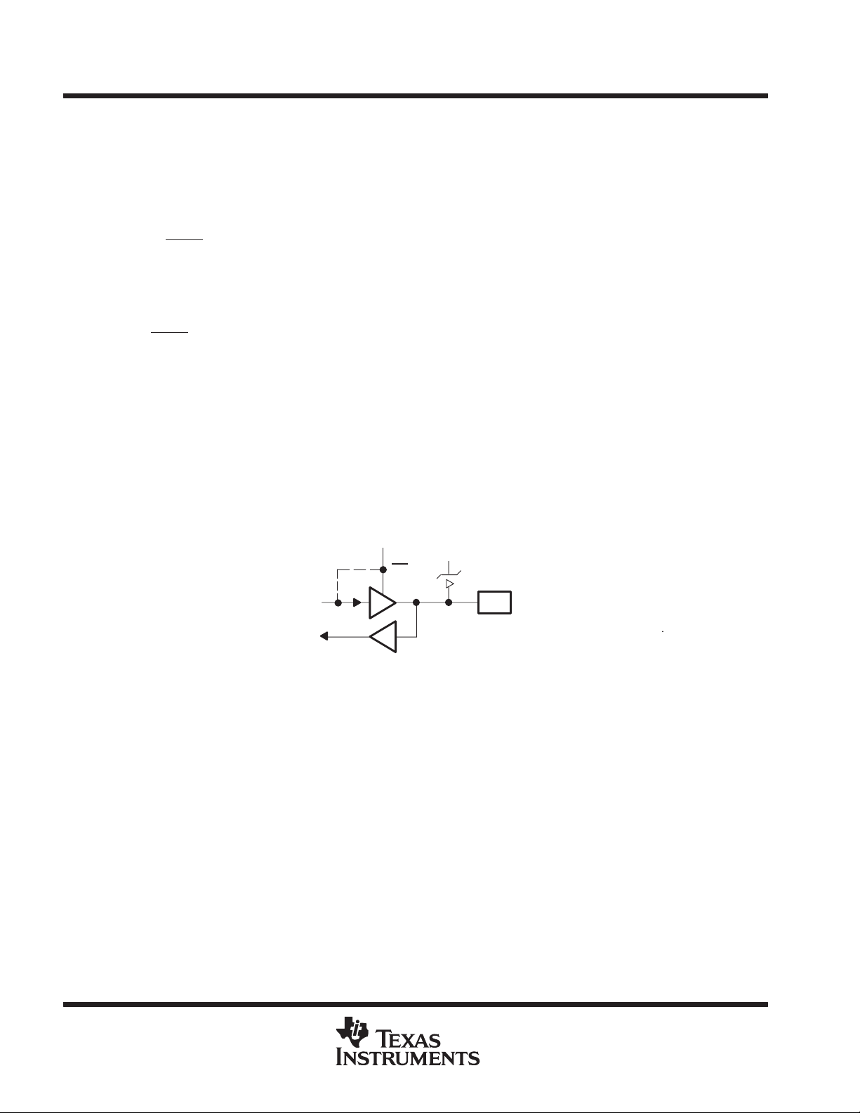
Figure 1 shows a 3-state bidirectional buffer. The
provides the electrical characteristics of the inputs and outputs.
NOTE:
The PCI1221 meets the ac specifications of the 1997 PC Card Standard and PCI Local Bus
Specification Rev. 2.2.
Tied for Open Drain
OE
recommended operating conditions
V
CCP
Pad
table, on page 120,
Figure 1. 3-State Bidirectional Buffer
NOTE:
Unused pins (input or I/O) must be held high or low to prevent them from floating.
clamping voltages
The clamping voltages are set to match whatever external environment the PCI1221 will be working with: 3.3
V or 5 V. The I/O sites can be pulled through a clamping diode to a voltage that protects the core from external
signals. The core power supply is always 3.3 V and is independent of the clamping voltages. For example, PCI
signaling can be either 3.3 V or 5 V, and the PCI1221 must reliably accommodate both voltage levels. This is
accomplished by using a 3.3-V I/O buffer that is 5-V tolerant, with the applicable clamping voltage applied. If
a system designer desires a 5-V PCI bus, V
The PCI1221 requires four separate clamping voltages because it supports a wide range of features. The four
voltages are listed and defined in the
22
recommended operating conditions
POST OFFICE BOX 655303 • DALLAS, TEXAS 75265
can be connected to a 5-V power supply.
CCP
, on page 112.
Page 23

PCI1221 GHK/PDV
PC CARD CONTROLLERS
SCPS042 – JULY 1998
peripheral component interconnect (PCI) interface
The PCI1221 is fully compliant with the PCI Local Bus Specification Rev. 2.2. The PCI1221 provides all required
signals for PCI master or slave operation, and may operate in either a 5-V of 3.3-V signaling environment by
connecting the V
PCI1221 provides the optional interrupt signals INTA and INTB.
PCI bus lock (LOCK)
The bus-locking protocol defined in the PCI specification is not highly recommended, but is provided on the
PCI1221 as an additional compatibility feature. The PCI LOCK signal can be routed to the MFUNC4 terminal
via the multifunction routing register, see the
Note that the use of LOCK is only supported by PCI-to-CardBus bridges in the downstream direction (away from
the processor).
PCI LOCK indicates an atomic operation that may require multiple transactions to complete. When LOCK is
asserted, nonexclusive transactions can proceed to an address that is not currently locked. A grant to start a
transaction on the PCI bus does not guarantee control of LOCK; control of LOCK is obtained under its own
protocol. It is possible for different initiators to use the PCI bus while a single master retains ownership of LOCK
Note that the CardBus signal for this protocol is CBLOCK to avoid confusion with the bus clock.
An agent may need to do an exclusive operation because a critical access to memory might be broken into
several transactions, but the master wants exclusive rights to a region of memory. The granularity of the lock
is defined by PCI to be 16 bytes, aligned. The lock protocol defined by PCI allows a resource lock without
interfering with nonexclusive real-time data transfer, such as video.
terminals to the desired voltage level. In addition to the mandatory PCI signals, the
CCP
multifunction routing register
description on page 62 for details.
.
The PCI bus arbiter may be designed to support only complete bus locks using the LOCK protocol. In this
scenario, the arbiter will not grant the bus to any other agent (other than the LOCK master) while LOCK is
asserted. A complete bus lock may have a significant impact on the performance of the video. The arbiter that
supports complete bus lock must grant the bus to the cache to perform a writeback due to a snoop to a modified
line when a locked operation is in progress.
The PCI1221 supports all LOCK protocol associated with PCI-to-PCI bridges, as also defined for
PCI-to-CardBus bridges. This includes disabling write posting while a locked operation is in progress, which can
solve a potential deadlock when using devices such as PCI-to-PCI bridges. The potential deadlock can occur
if a CardBus target supports delayed transactions and blocks access to the target until it completes a delayed
read. This target characteristic is prohibited by the 2.2 PCI specification, and the issue is resolved by the PCI
master using LOCK
loading subsystem identification
The subsystem vendor ID register and subsystem ID register make up a doubleword of PCI configuration space
located at offset 40h for functions 0 and 1. This doubleword register is used for system and option card (mobile
dock) identification purposes and is required by some operating systems. Implementation of this unique
identifier register is a PC 95 requirement.
The PCI1221 offers two mechanisms to load a read-only value into the subsystem registers. The first
mechanism relies upon the system BIOS providing the subsystem ID value. The default access mode to the
subsystem registers is read only , but can be made read/write by setting the SUBSYSRW bit in the system control
register (bit 5, at PCI offset 80h). Once this bit is set, the BIOS can write a subsystem identification value into
the registers at offset 40h. The BIOS must clear the SUBSYSRW bit such that the subsystem vendor ID register
and subsystem ID register is limited to read-only access. This approach saves the added cost of implementing
the serial electrically erasable programmable ROM (EEPROM).
.
POST OFFICE BOX 655303 • DALLAS, TEXAS 75265
23
Page 24
PCI1221 GHK/PDV
PC CARD CONTROLLERS
SCPS042 – JUL Y 1998
loading subsystem identification (continued)
In some conditions, such as in a docking environment, the subsystem vendor ID register and subsystem ID
register must be loaded with a unique identifier via a serial EEPROM. The PCI1221 loads the data from the serial
EEPROM after a reset of the primary bus. Note that the SUSPEND input gates the PCI reset from the entire
PCI1221 core, including the serial bus state machine (see
SUSPEND).
The PCI1221 provides a two-line serial bus host controller that can be used to interface to a serial EEPROM.
Refer to
serial bus interface
on page 29 for details on the two-wire serial bus controller and applications.
PC Card applications
This section describes the PC Card interfaces of the PCI1221:
D
Card insertion/removal and recognition
D
P2C power-switch interface
D
Zoom video support
D
Speaker and audio applications
D
LED socket activity indicators
D
CardBus socket registers
suspend mode
, on page 40, for details on using
PC Card insertion/removal and recognition
The 1997 PC Card Standard addresses the card-detection and recognition process through an interrogation
procedure that the socket must initiate on card insertion into a cold, nonpowered socket. Through this
interrogation, card voltage requirements and interface (16 bit versus CardBus) are determined.
The scheme uses the CD1, CD2, VS1, and VS2 signals (CCD1, CCD2, CVS1, and CVS2 for CardBus). The
configuration of these four terminals identifies the card type and voltage requirements of the PC Card interface.
The encoding scheme is defined in the 1997 PC Card Standard and in Table 5.
Table 5. PC Card Card-Detect and Voltage-Sense Connections
CD2//CCD2 CD1//CCD1 VS2//CVS2 VS1//CVS1 KEY INTERFACE VOLTAGE
Ground Ground Open Open 5 V 16-bit PC Card 5 V
Ground Ground Open Ground 5 V 16-bit PC Card 5 V and 3.3 V
Ground Ground Ground Ground 5 V 16-bit PC Card 5 V, 3.3 V, and X.X V
Ground Ground Open Ground LV 16-bit PC Card 3.3 V
Ground Connect to CVS1 Open Connect to CCD1 LV CardBus PC Card 3.3 V
Ground Ground Ground Ground LV 16-bit PC Card 3.3 V and X.X V
Connect to CVS2 Ground Connect to CCD2 Ground LV CardBus PC Card 3.3 V and X.X V
Connect to CVS1 Ground Ground Connect to CCD2 LV CardBus PC Card 3.3 V, X.X V, and Y.Y V
Ground Ground Ground Open LV 16-bit PC Card Y.Y V
Connect to CVS2 Ground Connect to CCD2 Open LV CardBus PC Card Y.Y V
Ground Connect to CVS2 Connect to CCD1 Open LV CardBus PC Card X.X V and Y.Y V
Connect to CVS1 Ground Open Connect to CCD2 LV CardBus PC Card Y.Y V
Ground Connect to CVS1 Ground Connect to CCD1 Reserved
Ground Connect to CVS2 Connect to CCD1 Ground Reserved
24
POST OFFICE BOX 655303 • DALLAS, TEXAS 75265
Page 25
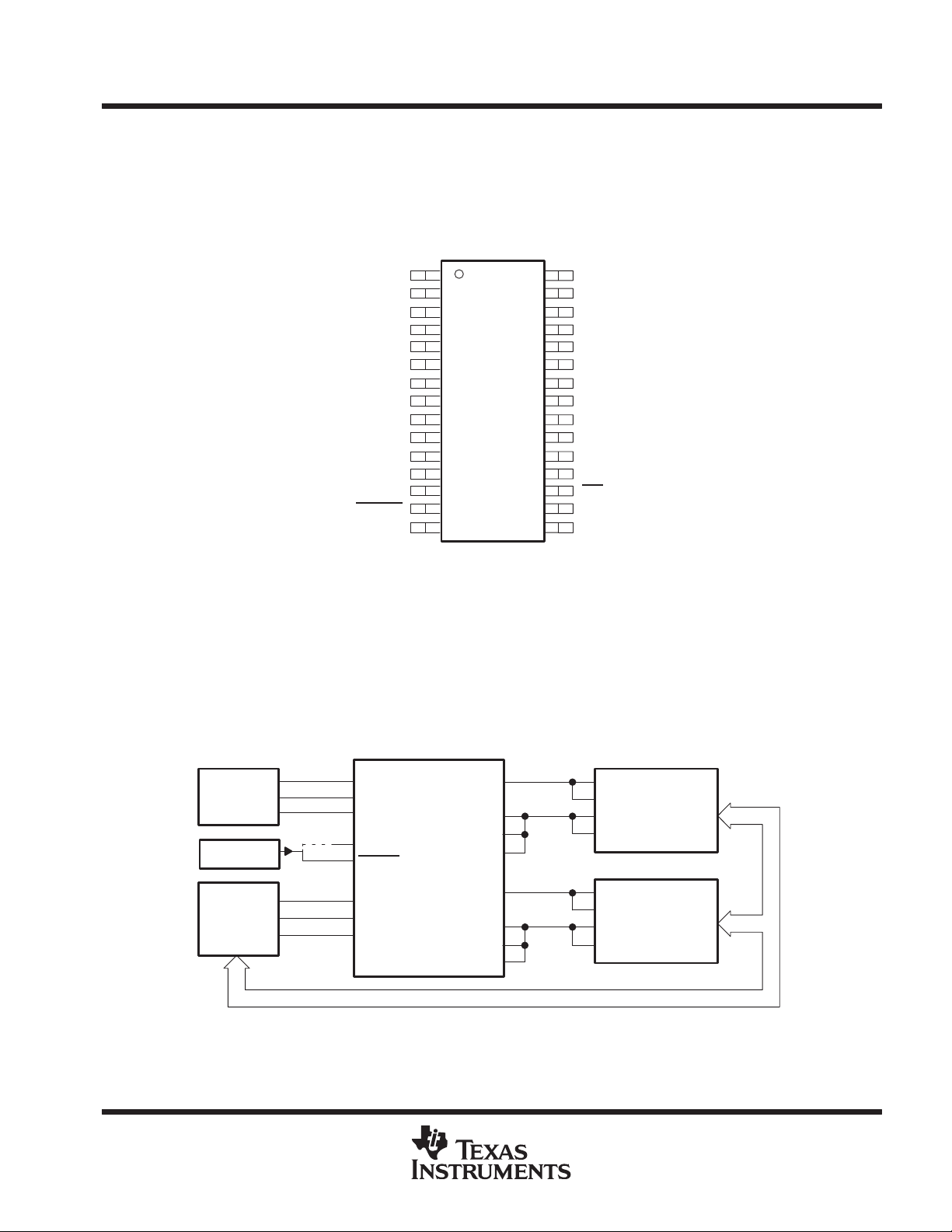
PCI1221 GHK/PDV
PC CARD CONTROLLERS
SCPS042 – JULY 1998
P2C power-switch interface (TPS2202A/2206)
The PCI1221 provides a P2C (PCMCIA Peripheral Control) interface for control of the PC Card power switch.
The CLOCK, DATA, and LATCH terminals interface with the TI TPS2202A/2206 dual-slot PC Card power
interface switches to provide power switch support. Figure 2 shows the terminal assignments of the TPS2206,
and Figure 3 illustrates a typical application where the PCI1221 represents the PCMCIA controller.
5 V
5 V
DATA
CLOCK
LATCH
RESET
12 V
A VPP
A VCC
A VCC
A VCC
GND
NC
RESET
3.3 V
NC – No internal connection
1
2
3
4
5
6
7
8
9
10
11
12
13
14
15
30
29
28
27
26
25
24
23
22
21
20
19
18
17
16
5 V
NC
NC
NC
NC
NC
12 V
BVPP
BVCC
BVCC
BVCC
NC
OC
3.3 V
3.3 V
Figure 2. TPS2206 Terminal Assignments
The CLOCK terminal on the PCI1221 can be an input or an output. The PCI1221 defaults the CLOCK terminal
as an input to control the serial interface and the internal state machine. The P2CCLK bit in the system control
register can be set by the platform BIOS to enable the PCI1221 to generate and drive the CLOCK internally from
the PCI clock. When the system design implements CLOCK as an output from the PCI1221, an external pull
down is required.
Power Supply
12 V
5 V
3.3 V
Supervisor
PCI1221
(PCMCIA
Controller)
TPS2206
12 V
5 V
3.3 V
RESET
RESET
CLOCK
DATA
LATCH
AVPP
AVCC
AVCC
AVCC
BVPP
BVCC
BVCC
BVCC
V
V
V
V
V
V
V
V
PP1
PP2
CC
CC
PP1
PP2
CC
CC
Figure 3. TPS2206 Typical Application
POST OFFICE BOX 655303 • DALLAS, TEXAS 75265
PC Card
A
PC Card
B
25
Page 26
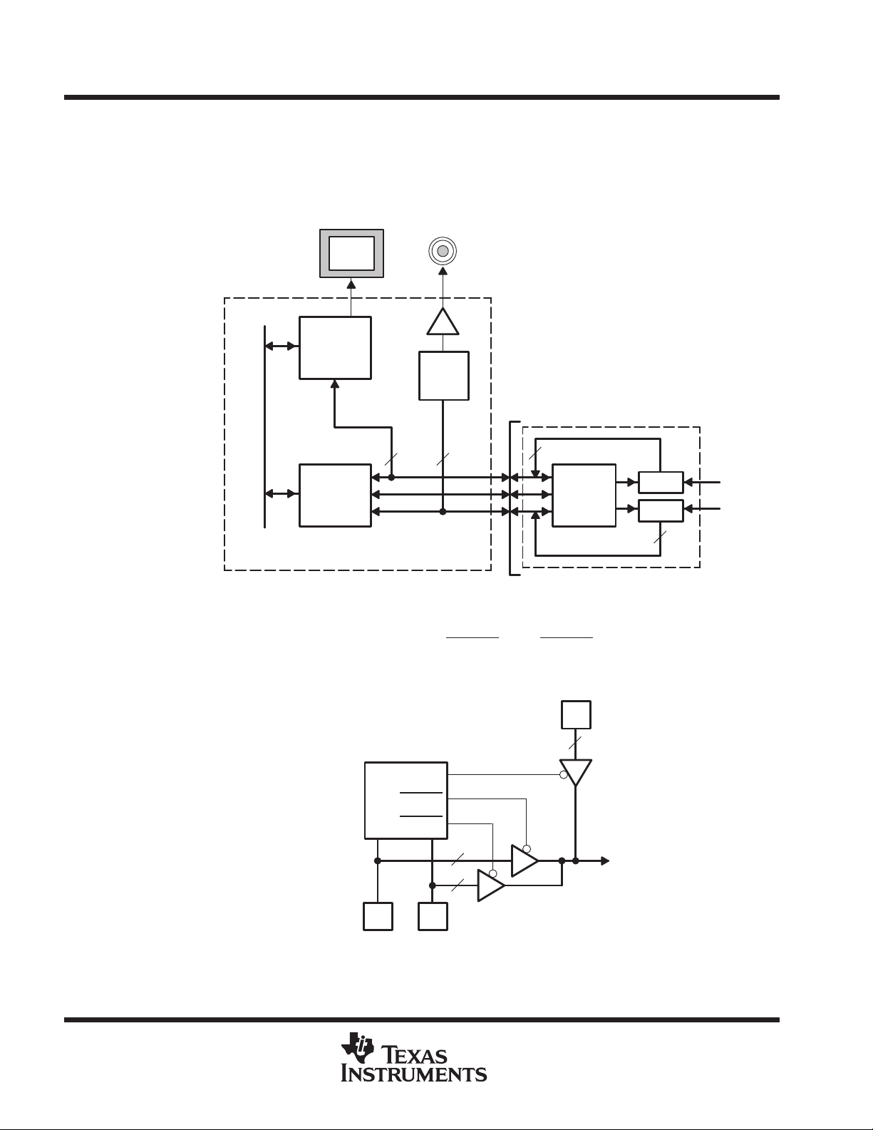
PCI1221 GHK/PDV
PC CARD CONTROLLERS
SCPS042 – JUL Y 1998
zoom video support
The PCI1221 allows for the implementation of zoom video for PC Cards. Zoom video is supported by setting
the ZVENABLE bit in the card control register on a per socket function basis. Setting this bit puts PC Card-16
address lines A25–A4 of the PC Card interface in the high-impedance state. These lines can then be used to
transfer video and audio data directly to the appropriate controller. Card address lines A3-A0 can still be used
to access PC Card CIS registers for PC Card configuration. Figure 4 illustrates a PCI1221 ZV implementation.
Audio
Codec
PCM
Audio
Input
Speakers
PC Card
19
PC Card
Interface
Video
Audio
4
CRT
Motherboard
PCI Bus
VGA
Controller
Zoom Video
Port
19 4
PCI1221
Figure 4. Zoom Video Implementation Using PCI1221
Not shown in Figure 4 is the multiplexing scheme used to route either socket 0 or socket 1 ZV source to the
graphics controller. The PCI1221 provides ZVSTAT, ZVSEL0, and ZVSEL1 signals on the multifunction
terminals to switch external bus drivers. Figure 5 shows an implementation for switching between three ZV
streams using external logic.
26
2
PCI1221
ZVSTAT
ZVSEL0
ZVSEL1
0 1
Figure 5. Zoom Video Switching Application
POST OFFICE BOX 655303 • DALLAS, TEXAS 75265
Page 27
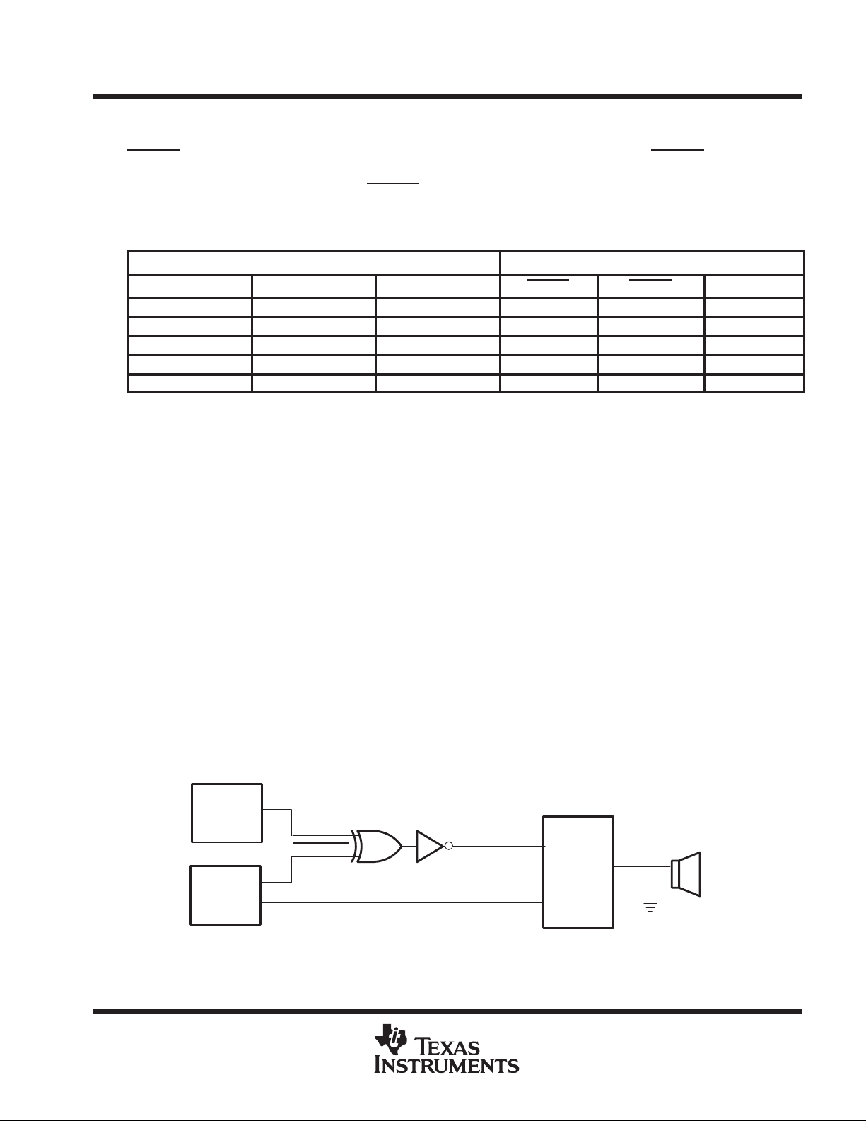
PCI1221 GHK/PDV
PC CARD CONTROLLERS
SCPS042 – JULY 1998
zoom video support (continued)
Figure 5 illustrates an implementation using standard three-state bus drivers with active-low output enables.
ZVSEL0 is an active-low output indicating that the Socket 0 ZV mode is enabled, and ZVSEL1 is an active-low
output indicating that Socket 1 ZV is enabled. When both sockets have ZV mode enabled, the PCI1221 defaults
to indicating socket 0 enabled through ZVSEL0; however , the PORTSEL bit in the card control register allows
software to select the socket ZV source priority. Table 6 illustrates the functionality of the ZV output signals.
Table 6. PC Card Card-Detect and Voltage-Sense Connections
INPUTS OUTPUTS
PORTSEL SOCKET 0 ENABLE SOCKET 1 ENABLE ZVSEL0 ZVSEL1 ZVSTAT
X 0 0 1 1 0
0 1 X 0 1 1
0 0 1 1 0 1
1 X 1 1 0 1
1 1 0 0 1 1
Also shown in Figure 5 is a third ZV source that may be provided from a source such as a high-speed serial bus
like IEEE1394. The ZVSTAT signal provides a mechanism to switch the third ZV source. ZVSTAT is an
active-high output indicating that one of the PCI1221 sockets is enabled for ZV mode. The implementation
shown in Figure 5 can be used if PC Card ZV is prioritized over other sources.
SPKROUT and CAUDPWM usage
SPKROUT carries the digital audio signal from the PC Card to the system. When a 16-bit PC Card is configured
for I/O mode, the BVD2 pin becomes SPKR. This terminal is also used in CardBus binary audio applications,
and is referred to as CAUDIO. SPKR
passes a TTL level digital audio signal to the PCI1221. The CardBus
CAUDIO signal also can pass a single-amplitude binary waveform. The binary audio signals from the two PC
Card Sockets are XOR’ed in the PCI1221 to produce SPKROUT. This output is enabled by the SPKROUTEN
bit in the card control register.
Older controllers support CAUDIO in binary or PWM mode but use the same pin (SPKROUT). Some audio chips
may not support both modes on one pin and may have a separate pin for binary and PWM. The PCI1221
implementation includes a signal for PWM, CAUDPWM, which can be routed to a MFUNC terminal. The
AUD2MUX bit located in the card control register is programmed on a per socket function basis to route a
CardBus CAUDIO PWM terminal to CAUDPWM. If both CardBus functions enable CAUDIO PWM routing to
CAUDPWM, then socket 0 audio takes precedence. Refer to the
multifunction routing register
description on
page 62 for details on configuring the MFUNC terminals.
Figure 6 provides an illustration of a sample application using SPKROUT and CAUDPWM.
System
Core Logic
BINARY_SPKR
Speaker
Subsystem
PWM_SPKR
PCI1221
SPKROUT
CAUDPWM
Figure 6. Sample Application of SPKROUT and CAUDPWM
POST OFFICE BOX 655303 • DALLAS, TEXAS 75265
27
Page 28
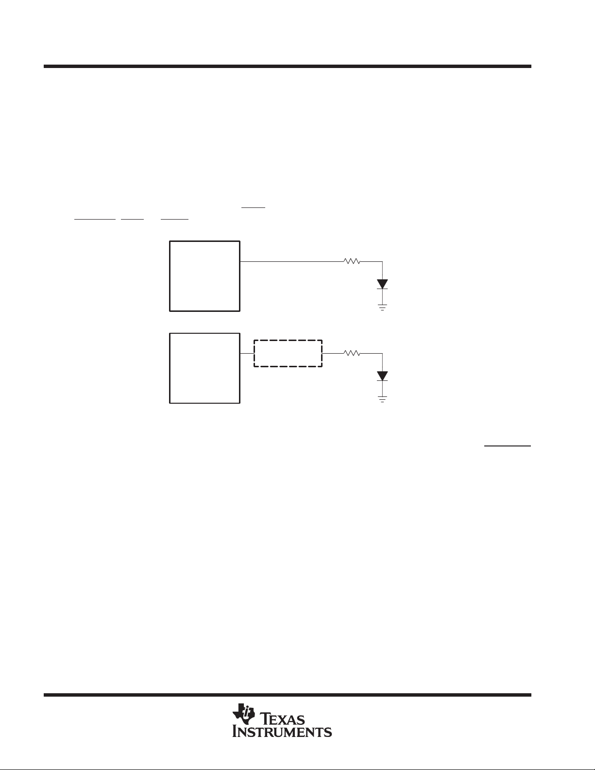
PCI1221 GHK/PDV
PC CARD CONTROLLERS
SCPS042 – JUL Y 1998
LED socket activity indicators
The socket activity LEDs are provided to indicate when a PC Card is being accessed. The LEDA1 and LEDA2
signals can be routed to the multifunction terminals. When configured for LED outputs, these terminals output
an active high signal to indicate socket activity. LEDA1 indicates socket 0 (card A) activity, and LEDA2 indicates
socket 1 (card B) activity. The LED_SKT output indicates socket activity to either socket 0 or socket 1. Refer
to the
multifunction routing register
The LED signal is active high and is driven for 64-ms durations. When the LED is not being driven high, it is driven
to a low state. Either of the two circuits shown in Figure 7 can be implemented to provide LED signaling, and
it is left for the board designer to implement the circuit that best fits the application.
The LED activity signals are valid when a card is inserted, powered, and not in reset. For PC Card 16, the LED
activity signals are pulsed when READY/IREQ is low. For CardBus cards, the LED activity signals are pulsed
if CFRAME, IRDY, or CREQ are active.
description on page 62 for details on configuring the multifunction terminals.
Current Limiting
R ≈ 500 Ω
PCI1221
PCI1221
Application-
Specific Delay
Current Limiting
R ≈ 500 Ω
LED
LED
Figure 7. T wo Sample LED Circuits
As indicated, the LED signals are driven for a period of 64 ms by a counter circuit. To avoid the possibility of
the LEDs appearing to be stuck when the PCI clock is stopped, the LED signaling is cut-off when the SUSPEND
signal is asserted, when the PCI clock is to be stopped during the clock run protocol, or when in the D2 or D1
power state.
If any additional socket activity occurs during this counter cycle, the counter is reset and the LED signal remains
driven. If socket activity is frequent (at least once every 64 ms), the LED signals remain driven.
CardBus socket registers
The PCI1221 contains all registers for compatibility with the latest PCI-to-PCMCIA CardBus bridge
specification. These registers exist as the CardBus socket registers, and are listed in Table 7.
28
POST OFFICE BOX 655303 • DALLAS, TEXAS 75265
Page 29
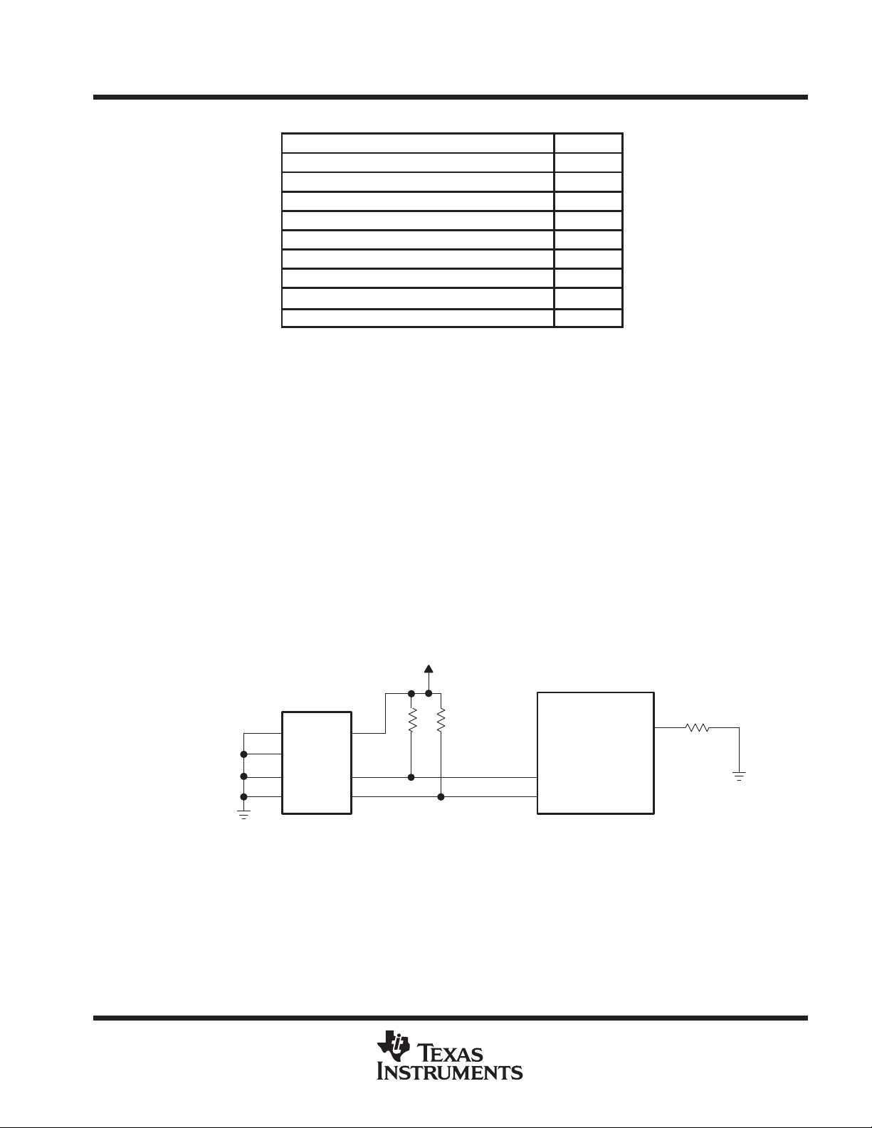
PCI1221 GHK/PDV
PC CARD CONTROLLERS
SCPS042 – JULY 1998
Table 7. CardBus Socket Registers
REGISTER NAME OFFSET
Socket event 00h
Socket mask 04h
Socket present state 08h
Socket force event 0Ch
Socket control 10h
Reserved 14h
Reserved 18h
Reserved 1Ch
Socket power management 20h
serial bus interface
The PCI1221 provides a serial bus interface to load subsystem identification and select register defaults through
a serial EEPROM and to provide a PC Card power switch interface alternative to P2C. Refer to
power-switch interface (TPS2202A/2206)
with various I2C and SMBus components.
on page 25 for details. The PCI1221 serial bus interface is compatible
P2C
serial bus interface implementation
The PCI1221 defaults to serial bus interface are disabled. To enable the serial interface, a pulldown resistor
must be implemented on the LATCH terminal and the appropriate pullup must be implemented on the SDA and
SCL signals, i.e. the MFUNC1 and MFUNC4 terminals. When the interface is detected, the SBDETECT bit in
the system control register is set. The SBDETECT bit is cleared by a write back of 1.
The PCI1221 implements a two pin serial interface with one clock signal (SCL) and one data signal (SDA). When
a pulldown is provided on the LATCH terminal, the SCL signal is mapped to the MFUNC4 terminal and the SDA
signal is mapped to the MFUNC1 terminal. The PCI1221 drives SCL at nearly 100 kHz during data transfers,
which is the maximum specified frequency for standard mode I2C. An example application implementing the
two-wire serial bus is illustrated in Figure 8.
V
CC
Serial
EEPROM
A0
A1
A2
SCL
SDA
PCI1221
LATCH
MFUNC4
MFUNC1
Figure 8. Serial EEPROM Application
Some serial device applications may include PC Card power switches, ZV source switches, card ejectors, or
other devices that may enhance the user’s PC Card experience. The serial EEPROM device and PC Card power
switches are discussed in the sections that follow.
serial bus interface protocol
The SCL and SDA signals are bidirectional, open-drain signals and require pullup resistors as shown in Figure
Figure 8. The PCI1221 supports up to 100 Kb/s data transfer rate and is compatible with standard mode I2C
using seven-bit addressing.
POST OFFICE BOX 655303 • DALLAS, TEXAS 75265
29
Page 30
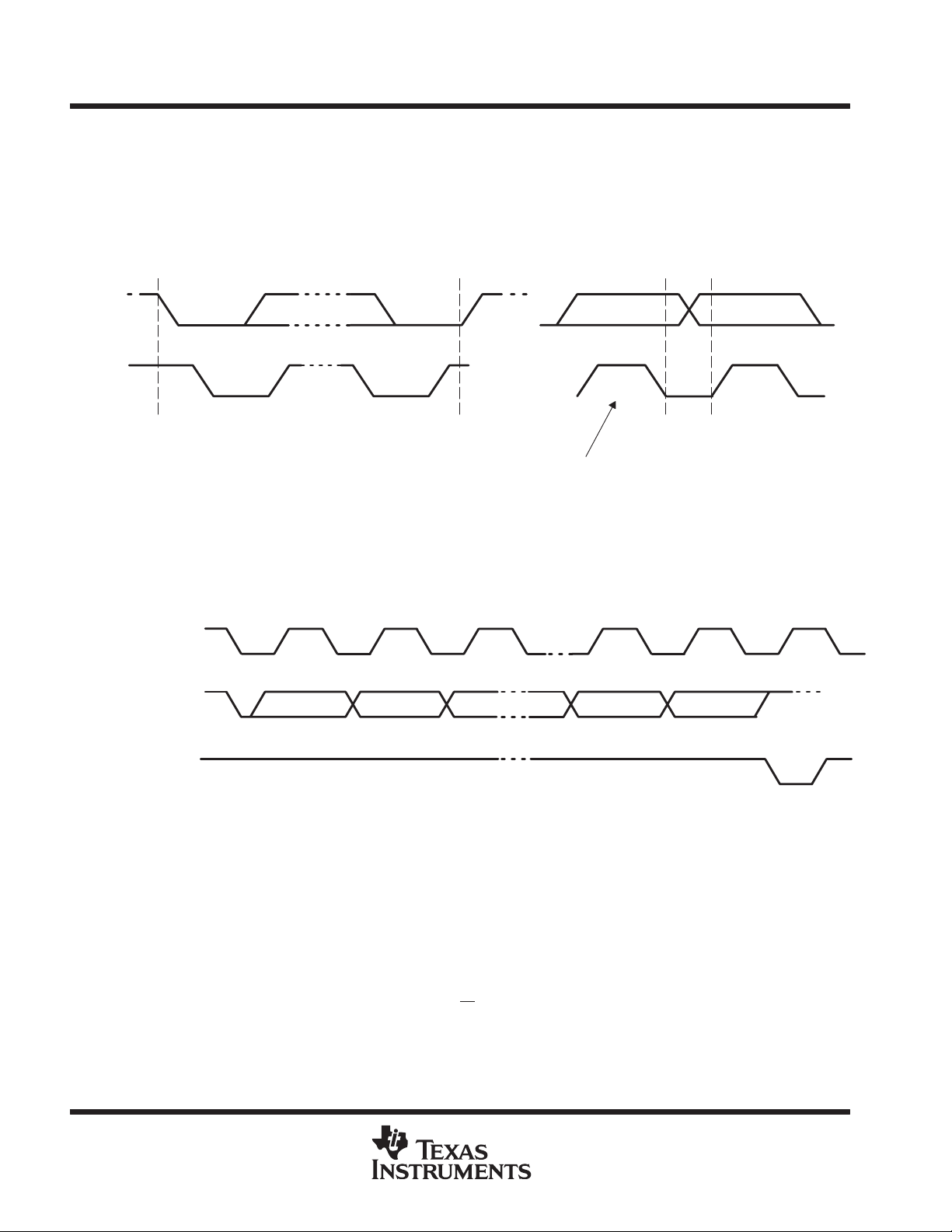
PCI1221 GHK/PDV
PC CARD CONTROLLERS
SCPS042 – JUL Y 1998
serial bus interface protocol (continued)
All data transfers are initiated by the serial bus master. The beginning of a data transfer is indicated by a start
condition, which is signalled when the SDA line transitions to low state while SCL is in the high state, as
illustrated in Figure 9. The end of a requested data transfer is indicated by a stop condition, which is signalled
by a low to high transition of SDA while SCL is in the high state, as shown in Figure 9. Data on SDA must remain
stable during the high state of the SCL signal, as changes on the SDA signal during the high state of SCL are
interpreted as control signals, that is, a start or a stop condition.
SDA
SCL
Start
Condition
Stop
Condition
Change of
Data Allowed
Data Line Stable,
Data Valid
Figure 9. Serial Bus Start/Stop Conditions and Bit Transfers
Data is transferred serially in 8-bit bytes. The number of bytes that may be transmitted during a data transfer
is unlimited, however, each byte must be completed with an acknowledge bit. An acknowledge (ACK) is
indicated by the receiver pulling the SDA signal low so that it remains low during the high state of the SCL signal.
The acknowledge protocol is illustrated in Figure 10.
SCL From
Master
SDA Output
By Transmitter
SDA Output
By Receiver
123 789
Figure 10. Serial Bus Protocol Acknowledge
The PCI1221 is a serial bus master; all other devices connected to the serial bus external to the PCI1221 are
slave devices. As the bus master, the PCI1221 drives the SCL clock at nearly 100 kHz during bus cycles and
three-states SCL (zero frequency) during idle states.
Typically, the PCI1221 masters byte reads and byte writes under software control. Doubleword reads are
performed by the serial EEPROM initialization circuitry upon a PCI reset and may not be generated under
software control. Refer to
serial bus EEPROM application
on page 32 for details on how the PCI1221
automatically loads the subsystem identification and other register defaults through a serial bus EEPROM.
A byte write is illustrated in Figure 11. The PCI1221 issues a start condition and sends the seven bit slave device
address and the command bit zero. A zero in the R/W command bit indicates that the data transfer is a write.
The slave device acknowledges if it recognizes the address. If there is no acknowledgment received by the
PCI1221, then an appropriate status bit is set in the serial bus control and status register. The word address
byte is then sent by the PCI1221 and another slave acknowledgment is expected. Then the PCI1221 delivers
the data byte MSB first and expects a final acknowledgment before issuing the stop condition.
30
POST OFFICE BOX 655303 • DALLAS, TEXAS 75265
Page 31

serial bus interface protocol (continued)
PCI1221 GHK/PDV
PC CARD CONTROLLERS
SCPS042 – JULY 1998
Slave Address Word Address
Sb6 b4b5 b3 b2 b1 b0 0 b7 b6 b5 b4 b3 b2 b1 b0AA
R/W
S/P = Start/stop conditionA = Slave acknowledgement
b7 b6 b4b5 b3 b2 b1 b0 A P
Data Byte
Figure 11. Serial Bus Protocol – Byte Write
A byte read is llustrated in Figure 12. The read protocol is very similar to the write protocol except the R/W
command bit must be set to one to indicate a read-data transfer. In addition, the PCI1221 master must
acknowledge reception of the read bytes from the slave transmitter. The slave transmitter drives the SDA signal
during read data transfers. The SCL signal remains driven by the PCI1221 master.
Slave Address Word Address
Sb6 b4b5 b3 b2 b1 b0 1 b7 b6 b5 b4 b3 b2 b1 b0AA
R/W
S/P = Start/stop conditionA = Slave acknowledgement
b7 b6 b4b5 b3 b2 b1 b0 M P
Data Byte
Figure 12. Serial Bus Protocol – Byte Read
Figure 13 illustrates EEPROM interface doubleword data collection protocol.
Slave Address Word Address
Slave Address
S1 10 0 0 0 0 0 b7 b6 b5 b4 b3 b2 b1 b0AA
Start
Data Byte 3 M
R/W
Data Byte 2 Data Byte 1 Data Byte 0 M PMM
M = Master acknowledgement
S1 10 00001A
Restart
S/P = Start/stop conditionA = Slave acknowledgement
Figure 13. EEPROM Interface doubleword Data Collection
R/W
POST OFFICE BOX 655303 • DALLAS, TEXAS 75265
31
Page 32

PCI1221 GHK/PDV
PC CARD CONTROLLERS
SCPS042 – JUL Y 1998
serial bus EEPROM application
When the PCI bus is reset and the serial bus interface is detected, the PCI1221 attempts to read the subsystem
identification and other register defaults from a serial EEPROM. The registers and corresponding bits that may
be loaded with defaults through the EEPROM are provided in Table 8.
Table 8. Registers and Bits Loadable Through Serial EEPROM
PCI OFFSET
40h 01h Subsystem identification 31–0
80h 02h System control register 31–29, 27, 26, 24, 15, 14, 6–3, 1
8Ch 03h Multifunction routing register 27–0
90h 04h Retry status, Card control, device control, diagnostic 31, 28–24, 22, 19–16, 15, 13, 7, 6
OFFSET
REFERENCE
REGISTER BITS LOADED FROM EEPROM
The EEPROM data format is detailed in Figure 14. This format must be followed for the PCI1221 to properly
load initializations from a serial EEPROM. Any undefined condition results in a terminated load and sets the
ROM_ERR bit in the serial bus control and status register.
Slave Address = 1010 000
Reference(0) Word Address 00h
Byte 3 (0) Word Address 01h
Byte 2 (0) Word Address 02h
Byte 1 (0) Word Address 03h
Byte 0 (0) Word Address 04h
RSVD
RSVD
RSVD
Reference(1) Word Address 08h
Reference(n) Word Address 8 × (n–1)
Byte 3 (n) Word Address 8 × (n–1) + 1
Byte 2 (n) Word Address 8 × (n–1) + 2
Byte 1 (n) Word Address 8 × (n–1) + 3
Byte 0 (n) Word Address 8 × (n–1) + 4
RSVD
RSVD
RSVD
EOL Word Address 8 × (n)
Figure 14. EEPROM Data Format
The byte at the EEPROM word address 00h must either contain a valid PCI offset, as listed in Table 8, or an
end-of-list (EOL) indicator. The EOL indicator is a byte value of FFh, and indicates the end of the data to load
from the EEPROM. Only doubleword registers are loaded from the EEPROM, and all bit fields must be
considered when programming the EEPROM.
The serial EEPROM is addressed at slave address 1010000b by the PCI1221. All hardware address bits for
the EEPROM should be tied to the appropriate level to achieve this address. The serial EEPROM chip in the
sample application circuit (Figure 8) assumes the 1010b high address nibble. The lower three address bits are
terminal inputs to the chip, and the sample application shows these terminal inputs tied to GND.
When a valid offset reference is read, four bytes are read from the EEPROM, MSB first, as illustrated in
Figure 13. The address autoincrements after every byte transfer according to the doubleword read protocol.
Note that the word addresses align with the data format illustrated in Figure 14. The PCI1221 continues to load
data from the serial EEPROM until an end-of-list indicator is read. Three reserved bytes are stuffed to maintain
eight byte data structures.
32
POST OFFICE BOX 655303 • DALLAS, TEXAS 75265
Page 33

PCI1221 GHK/PDV
PC CARD CONTROLLERS
SCPS042 – JULY 1998
serial bus EEPROM application (continued)
Note, the eight-byte data structure is important to provide correct addressing per the doubleword read format
shown in Figure 13. In addition, the reference offsets must be loaded in the EEPROM in sequential order, that
is 01h, 02h, 03h, 04h. If the offsets are not sequential, the registers may be loaded incorrectly.
serial bus power switch application
The PCI1221 does not automatically control a serial bus power switch transparently to host software as it does
2
C power switches. But, the PCI1221 serial bus interface can be used in conjunction with the power status,
for P
GPE,
output, and support software to control a serial bus power switch. If a serial bus power switch interface
is implemented, a pulldown resistor must be provided on the PCI1221 CLOCK terminal to reduce power
consumption.
The PCI1221 supports two common SMBus data write protocols, write byte and send byte formats. The write
byte protocol using a word address of 00h is discussed in
byte protocol is shown in Figure 15 using a slave address ‘101001x’. The PROT_SEL bit in the serial bus control
and status register, see Table 37 on page 79, allows the serial bus interface to operate with the send byte
protocol. For more information on programming the serial bus interface, refer to
through software
.
Slave Address Command Code
serial bus interface protocol
accessing serial bus devices
on page 29. The send
S1 10 0 0 1 X 0 b7 b6 b5 b4 b3 b2 b1 b0AA
R/W
S/P = Start/stop conditionA = Slave acknowledgement
P
Figure 15. Send Byte Protocol
The power switch may support an interrupt mode to indicate over current or other power switch related events.
The PCI1221 does not implement logic to respond to these events, but does implement a flexible general
purpose interface to control these events through ACPI and other handlers. Refer to
and Power Interface Specification
for details on implementing the PCI1221 in an ACPI system.
Advanced Configuration
accessing serial bus devices through software
The PCI1221 provides a programming mechanism to control serial bus devices through software. The
programming is accomplished through a doubleword of PCI configuration space at offset B0h. Table 9 lists the
registers used to program a serial bus device through software.
Table 9. PCI1221 Registers Used to Program Serial Bus Devices
PCI OFFSET REGISTER NAME DESCRIPTION
B0H Serial bus data
B1H Serial bus index
B2H
B3H
Serial bus slave
address
Serial bus control
and status
Contains the data byte to send on write commands or the received data byte on read
commands.
The content of this register is sent as the word address on byte writes or reads. This
register is not used in the quick command protocol.
Write transactions to this register initiate a serial bus transaction. The slave device address
and the R/W
Read data valid, general busy, and general error status are communicated through this
register. In addition, the protocol select bit is programmed through this register.
command selector are programmed through this register.
POST OFFICE BOX 655303 • DALLAS, TEXAS 75265
33
Page 34

PCI1221 GHK/PDV
PC CARD CONTROLLERS
SCPS042 – JUL Y 1998
programmable interrupt subsystem
Interrupts provide a way for I/O devices to let the microprocessor know that they require servicing. The dynamic
nature of PC Cards, and the abundance of PC Card I/O applications require substantial interrupt support from
the PCI1221. The PCI1221 provides several interrupt signaling schemes to accommodate the needs of a variety
of platforms. The different mechanisms for dealing with interrupts in this device are based on various
specifications and industry standards. The ExCA register set provides interrupt control for some 16-bit PC Card
functions, and the CardBus socket register set provides interrupt control for the CardBus PC Card functions.
The PCI1221 is, therefore, backward compatible with existing interrupt control register definitions, and new
registers have been defined where required.
The PCI1221 detects PC Card interrupts and events at the PC Card interface and notifies the host controller
using one of several interrupt signaling protocols. To simplify the discussion of interrupts in the PCI1221, PC
Card interrupts are classified as either card status change (CSC) or as functional interrupts.
The method by which any type of PCI1221 interrupt is communicated to the host interrupt controller varies from
system to system. The PCI1221 offers system designers the choice of using parallel PCI interrupt signaling,
parallel ISA-type IRQ interrupt signaling, or the IRQSER serialized ISA and/or PCI interrupt protocol. It is
possible to use the parallel PCI interrupts in combination with either parallel IRQs or serialized IRQs, as detailed
in the sections that follow. All interrupt signalling is provided through the seven multifunction terminals,
MFUNC0–6.
PC Card functional and card status change interrupts
PC Card functional interrupts are defined as requests from a PC Card application for interrupt service and are
indicated by asserting specially-defined signals on the PC Card interface. Functional interrupts are generated
by 16-bit I/O PC Cards and by CardBus PC Cards.
Card status change (CSC)-type interrupts are defined as events at the PC Card interface that are detected by
the PCI1221 and may warrant notification of host card and socket services software for service. CSC events
include both card insertion and removal from PC Card sockets, as well as transitions of certain PC Card signals.
Table 10 summarizes the sources of PC Card interrupts and the type of card associated with them. CSC and
functional interrupt sources are dependent on the type of card inserted in the PC Card socket. The three types
of cards that can be inserted into any PC Card socket are:
D
16-bit memory card
D
16-bit I/O card
D
CardBus cards
34
POST OFFICE BOX 655303 • DALLAS, TEXAS 75265
Page 35

16-bit I/O
CardBus
y
CSC
memory
PC Card functional and CSC interrupts (continued)
Table 10. Interrupt Mask and Flag Registers
CARD TYPE EVENT MASK FLAG
16-bit
memory
All 16-bit
PC Cards
Battery conditions
(BVD1, BVD2)
Wait states
(READY)
Change in card status
(STSCHG
Interrupt request
Power cycle complete
Change in card status
(CSTSCHG)
Interrupt request
Power cycle complete
Card insertion or
removal
(IREQ
(CINT
)
)
)
ExCA offset 05h/45h/805h
ExCA offset 05h/45h/805h
ExCA offset 05h/45h/805h
ExCA offset 05h/45h/805h
bits 1 and 0
bit 2
bit 0
Always enabled
bit 3
Socket mask
bit 0
Always enabled
Socket mask
bit 3
Socket mask
bits 2 and 1
PCI1221 GHK/PDV
PC CARD CONTROLLERS
SCPS042 – JULY 1998
ExCA offset 04h/44h/804h
bits 1 and 0
ExCA offset 04h/44h/804h
bit 2
ExCA offset 04h/44h/804h
bit 0
PCI configuration offset 91h
bit 0
ExCA offset 04h/44h/804h
bit 3
Socket event
bit 0
PCI configuration offset 91h
bit 0
Socket event
bit 3
Socket event
bits 2 and 1
Functional interrupt events are valid only for 16-bit I/O and CardBus cards; that is, the functional interrupts are
not valid for 16-bit memory cards. Furthermore, card insertion and removal-type CSC interrupts are
independent of the card type.
Table 11. PC Card Interrupt Events and Description
CARD TYPE EVENT TYPE SIGNAL DESCRIPTION
A transition on BVD1 indicates a change in the
PC Card battery conditions.
A transition on BVD2 indicates a change in the
PC Card battery conditions.
A transition on READY indicates a change in
the ability of the memory PC Card to accept or
provide data.
The assertion of STSCHG indicates a status
change on the PC Card.
The assertion of IREQ indicates an interrupt
request from the PC Card.
The assertion of CSTSCHG indicates a status
change on the PC Card.
The assertion of CINT indicates an interrupt
request from the PC Card.
A transition on either CD1//CCD1 or
CD2
//CCD2 indicates an insertion or removal
of a 16-bit or CardBus PC Card.
An interrupt is generated when a PC Card
power-up cycle has completed.
16-bit
16-bit I/O
CardBus
All PC Cards
Battery conditions
(BVD1, BVD2)
Wait states
(READY)
Change in
card status
(STSCHG)
Interrupt request
(IREQ)
Change in
card status
(CSTSCHG)
Interrupt request
(CINT
)
Card insertion
or removal
Power cycle
complete
BVD1(STSCHG)//CSTSCHG
BVD2(SPKR)//CAUDIO
CSC READY(IREQ)//CINT
CSC BVD1(STSCHG)//CSTSCHG
Functional READY(IREQ)//CINT
CSC BVD1(STSCHG)//CSTSCHG
Functional READY(IREQ)//CINT
CSC
CSC N/A
CD1//CCD1,
CD2
//CCD2
POST OFFICE BOX 655303 • DALLAS, TEXAS 75265
35
Page 36

PCI1221 GHK/PDV
PC CARD CONTROLLERS
SCPS042 – JUL Y 1998
PC Card functional and CSC interrupts (continued)
The naming convention for PC Card signals describes the function for 16-bit memory , I/O cards, and CardBus.
For example, READY(IREQ)//CINT includes READY for 16-bit memory cards, IREQ for 16-bit I/O cards, and
CINT for CardBus cards. The 16-bit memory card signal name is first, with the I/O card signal name second,
enclosed in parentheses. The CardBus signal name follows after a forward double slash (//).
The PC Card standard describes the power-up sequence that must be followed by the PCI1221 when an
insertion event occurs and the host requests that the socket VCC and VPP be powered. Upon completion of this
power-up sequence, the PCI1221 interrupt scheme can be used to notify the host system (see Table 11),
denoted by the power cycle complete event. This interrupt source is considered a PCI1221 internal event
because it depends on the completion of applying power to the socket rather than on a signal change at the PC
Card interface.
interrupt masks and flags
Host software may individually mask (or disable) most of the potential interrupt sources listed in Table 11 by
setting the appropriate bits in the PCI1221. By individually masking the interrupt sources listed, software can
control those events that cause a PCI1221 interrupt. Host software has some control over the system interrupt
the PCI1221 asserts by programming the appropriate routing registers. The PCI1221 allows host software to
route PC Card CSC and PC Card functional interrupts to separate system interrupts. Interrupt routing somewhat
specific to the interrupt signaling method used is discussed in more detail in the following sections.
When an interrupt is signaled by the PCI1221, the interrupt service routine must determine which of the events
listed in Table 10 caused the interrupt. Internal registers in the PCI1221 provide flags that report the source of
an interrupt. By reading these status bits, the interrupt service routine can determine the action to be taken.
T able 10 details the registers and bits associated with masking and reporting potential interrupts. All interrupts
can be masked except the functional PC Card interrupts, and an interrupt status flag is available for all types
of interrupts.
Notice that there is not a mask bit to stop the PCI1221 from passing PC Card functional interrupts through to
the appropriate interrupt scheme. These interrupts are not valid until the card is properly powered, and there
should never be a card interrupt that does not require service after proper initialization.
V arious methods of clearing the interrupt flag bits are listed in T able 10. The flag bits in the ExCA registers (16-bit
PC Card-related interrupt flags) can be cleared using two different methods. One method is an explicit write of
1 to the flag bit to clear, and the other is by reading the flag bit register . The selection of flag bit clearing is made
by bit 2 in the global control register (ExCA offset 1Eh/5Eh/81Eh), and defaults to the
read
method.
The CardBus-related interrupt flags can be cleared by an explicit write of 1 to the interrupt flag in the socket event
register. Although some of the functionality is shared between the CardBus registers and the ExCA registers,
software should not program the chip through both register sets when a CardBus card is functioning.
using parallel IRQ interrupts
The seven multifunction terminals, MFUNC6:0, implemented in the PCI1221 may be routed to obtain a subset
of the ISA IRQs . The IRQ choices provide ultimate flexibility in PC Card host interruptions. To use the parallel
ISA type IRQ interrupt signaling, software must program the device control register , located at PCI offset 92h,
to select the parallel IRQ signaling scheme. Refer to the
for details on configuring the multifunction terminals.
multifunction routing register
description on page 62
flag cleared on
A system using parallel IRQs requires (at a minimum) one PCI terminal, INTA, to signal CSC events. This
requirement is dictated by certain card and socket services software. The INTA requirement calls for routing
the MFUNC0 terminal for INT A signaling. The INTRTIE bit is used, in this case, to route socket 1 interrupt events
to INTA
36
. This leaves (at a maximum) six different IRQs to support legacy 16-bit PC Card functions.
POST OFFICE BOX 655303 • DALLAS, TEXAS 75265
Page 37
PCI1221 GHK/PDV
PC CARD CONTROLLERS
SCPS042 – JULY 1998
using parallel IRQ interrupts (continued)
As an example, suppose the six IRQs used by legacy PC Card applications are IRQ3, IRQ4, IRQ5, IRQ10,
IRQ11, and IRQ15. The multifunction control register must be programmed to a value of 0x0FBA5432. This
value routes the MFUNC0 terminal to INTA signaling and routes the remaining terminals as illustrated in
Figure 16. Not shown is that INTA must also be routed to the programmable interrupt controller (PIC), or to some
circuitry that provides parallel PCI interrupts to the host.
PCI1221 PIC
MFUNC1
MFUNC2
MFUNC3
MFUNC4
MFUNC5
MFUNC6
Figure 16. IRQ Implementation
Power-on software is responsible for programming the multifunction routing register to reflect the IRQ
configuration of a system implementing the PCI1221. The multifunction routing register is shared between the
two PCI1221 functions, and only one write to function 0 or 1 is necessary to configure the MFUNC6:0 signals.
Writing to only function 0 is recommended. Refer to the
multifunction routing register
for details on configuring the multifunction terminals.
IRQ3
IRQ4
IRQ5
IRQ10
IRQ11
IRQ15
description on page 62
The parallel ISA type IRQ signaling from the MFUNC6:0 terminals is compatible with those input directly into
the 8259 PIC. The parallel IRQ option is provided for system designs that require legacy ISA IRQs. Design
constraints may demand more MFUNC6:0 IRQ terminals than the PCI1221 makes available. A system designer
may choose to implement an IRQSER deserializer companion chip, such as the Texas Instruments PCI950.
T o use a deserializer , the MFUNC3 terminal must be configured as IRQSER and connected to the deserializer ,
which outputs all 15 ISA IRQ’s and four PCI interrupts as decoded from the IRQSER stream.
using parallel PCI interrupts
Parallel PCI interrupts are available when exclusively in parallel PCI interrupt mode parallel ISA IRQ signaling
mode, and when only IRQs are serialized with the IRQSER protocol. Both INTA and INTB can be routed to
MFUNC terminals (MFUNC0 and MFUNC1). However, both socket functions’ interrupts can be routed to INTA
(MFUNC0) if the INTRTIE bit is set in the system control register.
The INTRTIE bit effects the read-only value provided through accesses to the interrupt pin register. When
INTRTIE bit is set, both functions return a value of 0x01 on reads from the interrupt pin register for both parallel
and serial PCI interrupts. The interrupt signalling modes are summarized in Table 12.
POST OFFICE BOX 655303 • DALLAS, TEXAS 75265
37
Page 38

PCI1221 GHK/PDV
PC CARD CONTROLLERS
SCPS042 – JUL Y 1998
using parallel PCI interrupts (continued)
Table 12. Interrupt Pin Register Cross Reference
INTERRUPT SIGNALING MODE
Parallel PCI interrupts only 0 0x01 (INTA) 0x02 (INTB)
Parallel IRQ and parallel PCI interrupts 0 0x01 (INTA) 0x02 (INTB)
IRQ serialized (IRQSER) and parallel PCI interrupts 0 0x01 (INTA) 0x02 (INTB)
IRQ and PCI serialized (IRQSER) interrupts (default) 0 0x01 (INTA) 0x02 (INTB)
Parallel PCI interrupts only 1 0x01 (INTA) 0x01 (INTA)
Parallel IRQ and parallel PCI interrupts 1 0x01 (INTA) 0x01 (INTA)
IRQ serialized (IRQSER) and parallel PCI interrupts
IRQ and PCI serialized (IRQSER) interrupts
†
When configuring the PCI1221 functions to share PCI interrupts, multifunction terminal MFUNC3 must
be configured as IRQSER prior to setting the INTRTIE bit.
†
INTRTIE
BIT
†
1 0x01 (INTA) 0x01 (INTA)
1 0x01 (INTA) 0x01 (INTA)
INTPIN
FUNCTION 0
INTPIN
FUNCTION 1
using serialized IRQSER interrupts
The serialized interrupt protocol implemented in the PCI1221 uses a single terminal to communicate all interrupt
status information to the host controller. The protocol defines a serial packet consisting of a start cycle, multiple
interrupt indication cycles, and a stop cycle. All data in the packet is synchronous with the PCI clock. The packet
data describes sixteen parallel ISA IRQ signals and the optional four PCI interrupts INTA, INTB, INTC, and
INTD. For details on the IRQSER protocol refer to the document
Serialized IRQ Support for PCI Systems
SMI support in the PCI1221
The PCI1221 provides a mechanism for interrupting the system when power changes have been made to the
PC Card socket interfaces. The interrupt mechanism is designed to fit into a system maintenance interrupt (SMI)
scheme. SMI interrupts are generated by the PCI1221, when enabled, after a write cycle to either the socket
control register of the CardBus register set or the power control register of the ExCA register set causes a power
cycle change sequence sent on the power switch interface.
.
The SMI control is programmed through 3 bits in the system control register. These bits are SMIROUTE,
SMISTATUS, and SMIENB. The SMI control bits function as described in Table 13.
Table 13. SMI Control
BIT NAME FUNCTION
SMIROUTE This shared bit controls whether the SMI interrupts are sent as a CSC interrupt or as IRQ2.
SMISTAT This socket dependent bit is set when an SMI interrupt is pending. This status flag is cleared by writing back a 1.
SMIENB When set, SMI interrupt generation is enabled. This bit is shared by functions 0 and 1.
If CSC SMI interrupts are selected, then the SMI interrupt is sent as the CSC on a per socket basis. The CSC
interrupt can be either level or edge mode, depending upon the CSCMODE bit in the ExCA global control
register.
If IRQ2 is selected by SMIROUTE, the IRQSER signaling protocol supports SMI signaling in the IRQ2 IRQ/Data
slot. In a parallel ISA IRQ system, the support for an active low IRQ2 is provided only if IRQ2 is routed to either
MFUNC3 or MFUNC6 through the multifunction routing register.
38
POST OFFICE BOX 655303 • DALLAS, TEXAS 75265
Page 39

PCI1221 GHK/PDV
PC CARD CONTROLLERS
SCPS042 – JULY 1998
power management overview
TI has expended great effort to provide a high-performance device with low power consumption. In addition to
the low-power CMOS technology process used for the PCI1221, various features are designed into the device
to allow implementation of popular power-saving techniques. These features and techniques are discussed in
this section.
clock run protocol
The PCI CLKRUN feature is the primary method of power management on the PCI interface of the PCI1221.
CLKRUN
CLKRUN, this is not always available to the system designer, and alternate power savings features are
provided. For details on the CLKRUN protocol refer to the
The PCI1221 does not permit the central resource to stop the PCI clock under any of the following conditions:
D
D
D
D
D
D
signalling is provided through the MFUNC6 terminal. Since some chip sets do not implement
PCI Mobile Design Guide
The KEEPCLK bit in the system control register is set.
The PC Card-16 resource manager is busy.
The PCI1221 CardBus master state machine is busy. A cycle may be in progress on CardBus.
The PCI1221 master is busy. There may be posted data from CardBus to PCI in the PCI1221.
There are pending interrupts.
The CardBus CCLK for either socket has not been stopped by the PCI1221 CLKRUN manager.
.
The PCI1221 restarts the PCI clock using the CLKRUN protocol under any of the following conditions:
D
A PC Card-16 IREQ or a CardBus CINT has been asserted by either card.
D
A CardBus wakeup (CSTSCHG) or PC Card-16 STSCHG/RI event occurs in either socket.
D
A CardBus attempts to start the CCLK using CCLKRUN.
D
A CardBus card arbitrates for the CardBus bus using CREQ.
CardBus PC card power management
The PCI1221 implements its own card power management engine that can be used to turn off the CCLK to a
socket when there is no activity to the CardBus PC Card. The PCI clock-run protocol is followed on the CardBus
CCLKRUN
16-Bit PC card power mManagement
The COE and PWRDOWN bits in the ExCA registers are provided for 16-bit PC Card power management. The
COE bit three states the card interface to save power. The power savings when using this feature are minimal.
The COE bit will reset the PC Card when used, and the PWRDOWN bit will not. Furthermore, the PWRDOWN
bit is an automatic COE, that is, the PWRDOWN performs the COE function when there is no card activity.
interface to control this clock management.
NOTE:
The 16-bit PC Card must implement the proper pullup resistors for the COE and PWRDOWN
modes.
POST OFFICE BOX 655303 • DALLAS, TEXAS 75265
39
Page 40
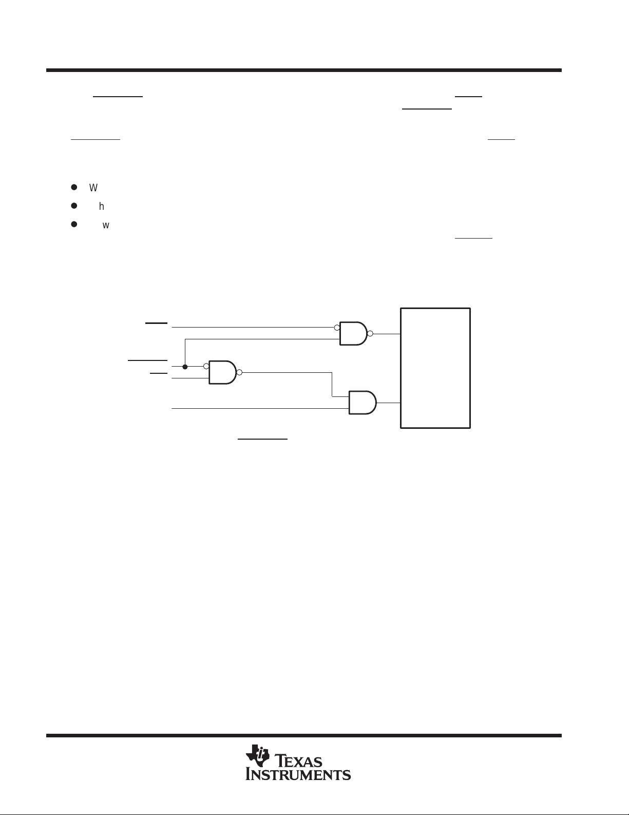
PCI1221 GHK/PDV
PC CARD CONTROLLERS
SCPS042 – JUL Y 1998
suspend mode
The SUSPEND signal provides backward compatibility and gates the PCI reset (PRST) signal from the
PCI1221. However, additional functionality has been defined for SUSPEND to provide additional
power-management options.
SUSPEND provides a mechanism to gate the PCLK from the PCI1221, as well as gate PRST. This can
potentially save power while in an idle state; however, it requires substantial design ef fort to implement. Some
issues to consider are:
D
What if cards are present in the sockets?
D
What if the cards in the sockets are powered?
D
How to pass CSC (insertion/removal) events.
Even without the PCI clock to the PCI1221 core, asynchronous-type functions (such as RI_OUT
events, wake-up events, etc., back to the system. If a system designer chooses to not pass card removal events
through to the system, then the PCI1221 would not be able to power down the empty socket without the power
switch clock (CLOCK) generated externally. Refer to the P2C power switch interface for details. Figure 17 is
a functional implementation diagram.
PRST
SUSPEND
GNT
PCLK
Figure 17. SUSPEND Functional Implementation
Figure 18 is a signal diagram of the suspend function.
PCI1221
Core
) can pass CSC
40
POST OFFICE BOX 655303 • DALLAS, TEXAS 75265
Page 41

suspend mode (continued)
PRST
GNT
SUSPEND
PCLK
PRSTIN
PCI1221 GHK/PDV
PC CARD CONTROLLERS
SCPS042 – JULY 1998
External T erminals
Internal Signals
SUSPENDIN
PCLKIN
Figure 18. Signal Diagram of Suspend Function
ring indicate
The RI_OUT output is an important feature in power management, allowing a system to go into a suspended
mode and wake up on modem rings and other card events. TI designed flexibility permits this signal to fit wide
platform requirements. RI_OUT on the PCI1221 can be asserted under any of the following conditions:
D
A 16-bit PC Card modem in a powered socket asserts RI to indicate to the system the presence of an
incoming call.
D
A powered down CardBus card asserts CSTSCHG (CBWAKE) requesting system and interface wake up.
D
A CSC event occurs, such as insertion/removal of cards, battery voltage levels.
CSTSCHG from a powered CardBus card is indicated as a CSC event, not as a CBWAKE event. These two
RI_OUT events are enabled separately . Figure 15 shows various enable bits for the PCI1221 RI_OUT function;
however, it does not show the masking of CSC events. See Table 10 for a detailed description of CSC interrupt
masks and flags.
POST OFFICE BOX 655303 • DALLAS, TEXAS 75265
41
Page 42

PCI1221 GHK/PDV
PC CARD CONTROLLERS
SCPS042 – JUL Y 1998
ring indicate (continued)
PC Card
Socket 0
PC Card
Socket 1
Card
I/F
Card
I/F
RI_OUT Function
CSTSMASK
CSC
RINGEN
RI
CDRESUME
CSC
CSTSMASK
CSC
RINGEN
RI
CDRESUME
RIENB
RI_OUT
CSC
Figure 19. RI_OUT Functional Diagram
RI from the 16-bit PC Card interface is masked by the ExCA control bit RINGEN in the interrupt and general
control register. This is programmed on a per-socket basis and is only applicable when a 16-bit card is powered
in the socket.
The CBWAKE signaling to RI_OUT is enabled through the same mask as the CSC event for CSTSCHG. The
mask bit, CSTSMASK, is programmed through the socket mask register in the CardBus socket registers.
PCI power management (PCIPM)
The PCI power-management (PCIPM) specification establishes the infrastructure required to let the operating
system control the power of PCI functions. This is done by defining a standard PCI interface and operations to
manage the power of PCI functions on the bus. The PCI bus and the PCI functions can be assigned one of four
software-visible power-management states that result in varying levels of power savings.
The four power-management states of PCI functions are:
D
D0 - Fully-on state
D
D1 and D2 - Intermediate states
D
D3 - Off state
Similarly , bus power states of the PCI bus are B0-B3. The bus power states B0-B3 are derived from the device
power state of the originating bridge device.
For the operating system (OS) to power manage the device power states on the PCI bus, the PCI function should
support four power-management operations. These operations are:
D
Capabilities reporting
D
Power status reporting
D
Setting the power state
D
System wake up
42
POST OFFICE BOX 655303 • DALLAS, TEXAS 75265
Page 43

PCI1221 GHK/PDV
PC CARD CONTROLLERS
SCPS042 – JULY 1998
PCI power management (PCIPM) (continued)
The OS identifies the capabilities of the PCI function by traversing the new capabilities list. The presence of new
capabilities is indicated by a 1 in the capabilities list (CAPLIST) bit in the status register (bit 4) and providing
access to a capabilities list.
The capabilities pointer provides access to the first item in the linked list of capabilities. For the PCI1221, a
CardBus bridge with PCI configuration space header type 2, the capabilities pointer is mapped to an offset
of 14h. The first byte of each capability register block is required to be a unique ID of that capability. PCI power
management has been assigned an ID of 01h. The next byte is a pointer to the next pointer item in the list of
capabilities. If there are no more items in the list, the next item pointer should be set to 0. The registers following
the next item pointer are specific to the function’s capability . The PCIPM capability implements the register block
outlined in Table 14.
Table 14. Power-Management Registers
REGISTER NAME OFFSET
Power-management capabilities Next item pointer Capability ID 0
Data PMCSR bridge support extensions Power-management control status (CSR) 4
The power management capabilities register is a static read-only register that provides information on the
capabilities of the function related to power management. The PMCSR register enables control of
power-management states and enables/monitors power-management events. The data register is an optional
register that can provide dynamic data.
For more information on PCI power management refer to the
Specification
.
PCI Bus Power Management Interface
ACPI support
The ACPI specification provides a mechanism that allows unique pieces of hardware to be described to the
ACPI driver. The PCI1221 offers a generic interface that is compliant with ACPI design rules.
Two doublewords of general purpose ACPI programming bits reside in PCI1221 PCI configuration space at
offset A8h. The programming model is broken into status and control functions. In compliance with ACPI, the
top level event status and enable bits reside in GPE_STS and GPE_EN registers. The status and enable bits
are implemented as defined by ACPI, and illustrated in Figure 20.
Status Bit
Event Input
Enable Bit
Event Output
Figure 20. Block Diagram of a Status/Enable Cell
The status and enable bits are used to generate an event that allows the ACPI driver to call a control method
associated with the pending status bit. The control method can then control the hardware by manipulating the
hardware control bits or by investigating child status bits and calling their respective control methods. A
hierarchical implementation would be somewhat limiting, however, as upstream devices would have to remain
in some level of power state to report events.
For more information of ACPI refer to the
Advanced Configuration and Power Interface Specification.
POST OFFICE BOX 655303 • DALLAS, TEXAS 75265
43
Page 44

PCI1221 GHK/PDV
PC CARD CONTROLLERS
SCPS042 – JUL Y 1998
PC Card controller programming model
This section describes the PCI1221 PCI configuration registers that make up the 256-byte PCI configuration
header for each PCI1221 function. As noted, some bits are global in nature and should be accessed only
through function 0.
PCI configuration registers (functions 0 and 1)
The PCI1221 is a multifunction PCI device, and the PC Card controller is integrated as PCI functions 0 and 1.
The configuration header is compliant with the PCI specification as a CardBus bridge header and is PC 99
compliant as well. Table 15 shows the PCI configuration header, which includes both the predefined portion of
the configuration space and the user-definable registers.
Table 15. PCI Configuration Registers (Functions 0 and 1)
REGISTER NAME OFFSET
Device ID Vendor ID 00h
Status Command 04h
Class code Revision ID 08h
BIST Header type Latency timer Cache line size 0Ch
CardBus socket/ExCA base address 10h
Secondary status Reserved Capability pointer 14h
CardBus latency timer Subordinate bus number CardBus bus number PCI bus number 18h
CardBus Memory base register 0 1Ch
CardBus Memory limit register 0 20h
CardBus Memory base register 1 24h
CardBus Memory limit register 1 28h
CardBus I/O base register 0 2Ch
CardBus I/O limit register 0 30h
CardBus I/O base register 1 34h
CardBus I/O limit register 1 38h
Bridge control Interrupt pin Interrupt line 3Ch
Subsystem ID Subsystem vendor ID 40h
PC Card 16-bit I/F legacy-mode base address 44h
Reserved 48h–7Ch
System control 80h
Reserved 84h–88h
Multifunction routing 8Ch
Diagnostic Device control Card control Retry status 90h
Reserved 94h-9Fh
Power-management capabilities Next-item pointer Capability ID A0h
PM data
General-purpose event enable General-purpose event status A8h
General-purpose output General-purpose input ACh
Serial bus control/status Serial bus slave address Serial bus index Serial bus data B0h
PMCSR bridge support
extensions
Power-management control/status A4h
Reserved B4h–FCh
44
POST OFFICE BOX 655303 • DALLAS, TEXAS 75265
Page 45

PCI1221 GHK/PDV
PC CARD CONTROLLERS
SCPS042 – JULY 1998
vendor ID register
Bit 15 14 13 12 11 10 9 8 7 6 5 4 3 2 1 0
Name Vendor ID
Type R R R R R R R R R R R R R R R R
Default 0 0 0 1 0 0 0 0 0 1 0 0 1 1 0 0
Register: Vendor ID
Type: Read only
Offset: 00h (functions 0, 1)
Default: 104Ch
Description: This 16-bit read-only register contains a value allocated by the PCI SIG (special interest
group) and identifies the manufacturer of the PCI device. The vendor ID assigned to TI is
104Ch.
device ID register
Bit 15 14 13 12 11 10 9 8 7 6 5 4 3 2 1 0
Name Device ID
Type R R R R R R R R R R R R R R R R
Default 1 0 1 0 1 1 0 0 0 0 0 1 1 0 0 1
Register: Device ID
Type: Read only
Offset: 02h (functions 0, 1)
Default: AC19h
Description: This 16-bit read-only register contains a value assigned to the PCI1221 by TI. The device
identification for the PCI1221 is AC19h.
command register
Bit 15 14 13 12 11 10 9 8 7 6 5 4 3 2 1 0
Name Command
Type R R R R R R R R/W R R/W R R R R/W R/W R/W
Default 0 0 0 0 0 0 0 0 0 0 0 0 0 0 0 0
Register: Command
Type: Read only, read/write (see individual bit descriptions)
Offset: 04h
Default: 0000h
Description: The command register provides control over the PCI1221 interface to the PCI bus. All bit
functions adhere to the definitions in PCI Local Bus Specification 2.2. None of the bit functions
in this register are shared between the two PCI1221 PCI functions. Two command registers
exist in the PCI1221, one for each function. Software must manipulate the two PCI1221
functions as separate entities when enabling functionality through the command register. The
SERR_EN and PERR_EN enable bits in this register are internally wired-OR between the two
functions, and these control bits appear separately according to their software function. See
Table 16 for the complete description of the register contents.
POST OFFICE BOX 655303 • DALLAS, TEXAS 75265
45
Page 46

PCI1221 GHK/PDV
PC CARD CONTROLLERS
SCPS042 – JUL Y 1998
T able 16. Command Register
BIT SIGNAL TYPE FUNCTION
15–10 RSVD R Reserved. Bits 15–10 are read only and return 0s when read. Write transactions have no effect.
9 FBB_EN R
8 SERR_EN R/W
7 STEP_EN R
6 PERR_EN R/W
5 VGA_EN R
4 MWI_EN R
3 SPECIAL R
2 MAST_EN R/W
1 MEM_EN R/W
0 IO_EN R/W
Fast back-to-back enable. The PCI1221 does not generate fast back-to-back transactions; therefore, bit
9 is read only and returns 0s when read.
System Error (SERR) enable. Bit 8 controls the enable for the SERR driver on the PCI interface. SERR
can be asserted after detecting an address parity error on the PCI bus. Both bit 8 and bit 6 must be set
for the PCI1221 to report address parity errors.
Address/data stepping control. The PCI1221 does not support address/data stepping, and bit 7 is
hardwired to 0. Write transactions to this bit have no effect.
Parity error response enable. Bit 6 controls the PCI1221’s response to parity errors through PERR. Data
parity errors are indicated by asserting PERR
SERR
VGA palette snoop. Bit 5 controls how PCI devices handle accesses to video graphics array (VGA) palette
registers. The PCI1221 does not support VGA palette snooping; therefore, this bit is hardwired to 0. Bit
5 is read only and returns 0 when read. Write transactions to this bit have no effect.
Memory write and invalidate enable. Bit 4 controls whether a PCI initiator device can generate memory
write and Invalidate commands. The PCI1221 controller does not support memory write and invalidate
commands, it uses memory write commands instead; therefore, this bit is hardwired to 0. Bit 4 is read only
and returns 0 when read. Write transactions to this bit have no effect.
Special cycles. Bit 3 controls whether or not a PCI device ignores PCI special cycles. The PCI1221 does
not respond to special cycle operations; therefore, this bit is hardwired to 0. Bit 3 is read only and returns
0 when read. Write transactions to this bit have no effect.
Bus master control. Bit 2 controls whether or not the PCI1221 can act as a PCI bus initiator (master). The
PCI1221 can take control of the PCI bus only when this bit is set.
Memory space enable. Bit 1 controls whether or not the PCI1221 can claim cycles in PCI memory space.
I/O space control. Bit 0 controls whether or not the PCI1221 can claim cycles in PCI I/O space.
0 = Disable SERR
1 = Enable SERR
.
0 = PCI1221 ignores detected parity error (default)
1 = PCI1221 responds to detected parity errors
0 = Disables the PCI1221’s ability to generate PCI bus accesses (default)
1 = Enables the PCI1221’s ability to generate PCI bus accesses
0 = Disables the PCI1221’s response to memory space accesses (default)
1 = Enables the PCI1221’s response to memory space accesses
0 = Disables the PCI1221 from responding to I/O space accesses (default)
1 = Enables the PCI1221 to respond to I/O space accesses
output driver (default)
output driver
, whereas address parity errors are indicated by asserting
46
POST OFFICE BOX 655303 • DALLAS, TEXAS 75265
Page 47

PCI1221 GHK/PDV
PC CARD CONTROLLERS
SCPS042 – JULY 1998
status register
Bit 15 14 13 12 11 10 9 8 7 6 5 4 3 2 1 0
Name Status
Type R/C R/C R/C R/C R/C R R R/C R R R R R R R R
Default 0 0 0 0 0 0 1 0 0 0 0 1 0 0 0 0
Register: Status
Type: Read only, read/clear (see individual bit descriptions)
Offset: 06h (functions 0, 1)
Default: 0210h
Description: The status register provides device information to the host system. Bits in this register may be
read normally. A bit in the status register is reset when a 1 is written to that bit location; a 0
written to a bit location has no effect. All bit functions adhere to the definitions in the PCI Local
Bus Specification 2.2. PCI bus status is shown through each function. See Table 17 for the
complete description of the register contents.
Table 17. Status Register
BIT SIGNAL TYPE FUNCTION
15 PAR_ERR R/C Detected parity error. Bit 15 is set when a parity error is detected (either address or data).
14 SYS_ERR R/C
13 MABORT R/C
12 TABT_REC R/C
11 TABT_SIG R/C
10–9 PCI_SPEED R
8 DATAPAR R/C
7 FBB_CAP R
6 UDF R
5 66MHZ R
4 CAPLIST R
3–0 RSVD R Reserved. Bits 3–0 return 0s when read.
Signaled system error. Bit 14 is set when SERR is enabled and the PCI1221 signals a system error to the
host.
Received master abort. Bit 13 is set when a cycle initiated by the PCI1221 on the PCI bus has been
terminated by a master abort.
Received target abort. Bit 12 is set when a cycle initiated by the PCI1221 on the PCI bus was terminated
by a target abort.
Signaled target abort. Bit 11 is set by the PCI1221 when it terminates a transaction on the PCI bus with
a target abort.
DEVSEL timing. These read-only bits encode the timing of DEVSEL and are hardwired 01b, indicating that
the PCI1221 asserts PCI_SPEED at a medium speed on nonconfiguration cycle accesses.
Data parity error detected.
Fast back-to-back capable. The PCI1221 cannot accept fast back-to-back transactions; thus, bit 7 is
hardwired to 0.
User-definable feature support. The PCI1221 does not support the user-definable features; thus, bit 6 is
hardwired to 0.
66-MHz capable. The PCI1221 operates at a maximum PCLK frequency of 33 MHz; therefore, bit 5 is
hardwired to 0.
Capabilities list. Bit 4 is read only and returns 1 when read. This bit indicates that capabilities in addition
to standard PCI capabilities are implemented. The linked list of PCI power-management capabilities is
implemented in this function.
0 = The conditions for setting bit 8 have not been met.
1 = A data parity error occurred, and the following conditions were met:
a. PERR
b. The PCI1221 was the bus master during the data parity error.
c. The parity error response bit is set in the command.
was asserted by any PCI device including the PCI1221.
POST OFFICE BOX 655303 • DALLAS, TEXAS 75265
47
Page 48

PCI1221 GHK/PDV
PC CARD CONTROLLERS
SCPS042 – JUL Y 1998
revision ID register
Bit 7 6 5 4 3 2 1 0
Name Revision ID
Type R R R R R R R R
Default 0 0 0 0 0 0 0 0
Register: Revision ID
Type: Read only
Offset: 08h (functions 0, 1)
Default: 00h
Description: This read-only register indicates the silicon revision of the PCI1221.
PCI class code register
Bit 23 22 21 20 19 18 17 16 15 14 13 12 11 10 9 8 7 6 5 4 3 2 1 0
Name Class code
Base class Sub class Programming interface
Type R R R R R R R R R R R R R R R R R R R R R R R R
Default 0 0 0 0 0 1 1 0 0 0 0 0 0 1 1 1 0 0 0 0 0 0 0 0
Register: PCI Class code
Type: Read only
Offset: 09h (functions 0, 1)
Default: 060700h
Description: The class code register recognizes the PCI1221 functions 0 and 1 as a bridge device (06h),
and CardBus bridge device (07h) with a 00h programming interface.
cache line size register
Bit 7 6 5 4 3 2 1 0
Name Cache line size
Type R/W R/W R/W R/W R/W R/W R/W R/W
Default 0 0 0 0 0 0 0 0
Register: Cache line size
Type: Read/write
Offset: 0Ch (functions 0, 1)
Default: 00h
Description: The cache line size register is programmed by host software to indicate the system cache line
size.
48
POST OFFICE BOX 655303 • DALLAS, TEXAS 75265
Page 49

PCI1221 GHK/PDV
PC CARD CONTROLLERS
SCPS042 – JULY 1998
latency timer register
Bit 7 6 5 4 3 2 1 0
Name Latency timer
Type R/W R/W R/W R/W R/W R/W R/W R/W
Default 0 0 0 0 0 0 0 0
Register: Latency timer
Type: Read/write
Offset: 0Dh
Default: 00h
Description: The latency timer register specifies the latency timer for the PCI1221 in units of PCI clock
cycles. When the PCI1221 is a PCI bus initiator and asserts FRAME
counting from zero. If the latency timer expires before the PCI1221 transaction has
terminated, the PCI1221 terminates the transaction when its GNT is deasserted. This register
is separate for each of the two PCI1221 functions. This allows platforms to prioritize the two
PCI1221 functions’ use of the PCI bus.
header type register
Bit 7 6 5 4 3 2 1 0
Name Header type
Type R R R R R R R R
Default 1 0 0 0 0 0 1 0
, the latency timer begins
Register: Header type
Type: Read only
Offset: 0Eh (functions 0, 1)
Default: 82h
Description: This read-only register returns 82h when read, indicating that the PCI1221 functions 0 and 1
configuration spaces adhere to the CardBus bridge PCI header. The CardBus bridge PCI
header ranges from PCI register 0 to 7Fh, and 80h–FFh is user-definable extension registers.
BIST register
Bit 7 6 5 4 3 2 1 0
Name BIST
Type R R R R R R R R
Default 0 0 0 0 0 0 0 0
Register: BIST
Type: Read only
Offset: 0Fh (functions 0, 1)
Default: 00h
Description: Because the PCI1221 does not support a built-in self-test (BIST), this register is read only and
returns the value of 00h when read.
POST OFFICE BOX 655303 • DALLAS, TEXAS 75265
49
Page 50

PCI1221 GHK/PDV
PC CARD CONTROLLERS
SCPS042 – JUL Y 1998
CardBus socket registers/ExCA base-address register
Bit 31 30 29 28 27 26 25 24 23 22 21 20 19 18 17 16
Name CardBus socket/ExCA base address
Type R/W R/W R/W R/W R/W R/W R/W R/W R/W R/W R/W R/W R/W R/W R/W R/W
Default 0 0 0 0 0 0 0 0 0 0 0 0 0 0 0 0
Bit 15 14 13 12 11 10 9 8 7 6 5 4 3 2 1 0
Name CardBus socket/ExCA base address
Type R/W R/W R/W R/W R R R R R R R R R R R R
Default 0 0 0 0 0 0 0 0 0 0 0 0 0 0 0 0
Register: CardBus socket/ExCA base address
Type: Read only, read/write
Offset: 10h
Default: 0000 0000h
Description: The CardBus socket registers/ExCA base-address register is programmed with a base
address referencing the CardBus socket registers and the memory-mapped ExCA register
set. Bits 31-12 are read/write, and allow the base address to be located anywhere in the 32-bit
PCI memory address space on a 4K-byte boundary. Bits 11-0 are read only, returning 0s
when read. When software writes all 1s to this register, the value readback is FFFF F000h,
indicating that at least 4K-bytes of memory address space are required. The CardBus
registers start at offset 000h, and the memory-mapped ExCA registers begin at offset 800h.
Since this register is not shared by functions 0 and 1, mapping of each socket control is
performed separately.
capability pointer register
Bit 7 6 5 4 3 2 1 0
Name Capability pointer
Type R R R R R R R R
Default 1 0 1 0 0 0 0 0
Register: Capability pointer
Type: Read only
Offset: 14h
Default: A0h
Description: The capability pointer register provides a pointer into the PCI configuration header where the
PCI power management register block resides. PCI header doublewords at A0h and A4h
provide the power management (PM) registers. Each socket has its own capability pointer
register. This register is read only and returns A0h when read.
50
POST OFFICE BOX 655303 • DALLAS, TEXAS 75265
Page 51

PCI1221 GHK/PDV
PC CARD CONTROLLERS
SCPS042 – JULY 1998
secondary status register
Bit 15 14 13 12 11 10 9 8 7 6 5 4 3 2 1 0
Name Secondary status
Type R/C R/C R/C R/C R/C R R R/C R R R R R R R R
Default 0 0 0 0 0 0 1 0 0 0 0 0 0 0 0 0
Register: Secondary status
Type: Read only, read/clear (see individual bit descriptions)
Offset: 16h
Default: 0200h
Description: The secondary status register is compatible with the PCI-to-PCI bridge secondary status
register, and indicates CardBus-related device information to the host system. This register is
very similar to the PCI status register (offset 06h); status bits are cleared by writing a 1.
Table 18. Secondary Status Register
BIT SIGNAL TYPE FUNCTION
15 CBPARITY R/C Detected parity error . Bit 15 is set when a CardBus parity error is detected (either address or data).
14 CBSERR R/C
13 CBMABORT R/C
12 REC_CBTA R/C
11 SIG_CBTA R/C
10–9 CB_SPEED R
8 CB_DPAR R/C
7 CBFBB_CAP R
6 CB_UDF R
5 CB66MHZ R
4–0 RSVD R Reserved. Bits 4–0 return 0s when read.
Signaled system error. Bit 14 is set when CSERR is signaled by a CardBus card. The PCI1221 does not
assert CSERR
Received master abort. Bit 13 is set when a cycle initiated by the PCI1221 on the CardBus bus has been
terminated by a master abort.
Received target abort. Bit 12 is set when a cycle initiated by the PCI1221 on the CardBus bus is
terminated by a target abort.
Signaled target abort. Bit 1 1 is set by the PCI1221 when it terminates a transaction on the CardBus bus
with a target abort.
CDEVSEL timing. These read-only bits encode the timing of CDEVSEL and are hardwired 01b,
indicating that the PCI1221 asserts CB_SPEED at a medium speed.
CardBus data parity error detected.
Fast back-to-back capable. The PCI1221 cannot accept fast back-to-back transactions; thus, bit 7 is
hardwired to 0.
User-definable feature support. The PCI1221 does not support the user-definable features; thus, bit 6
is hardwired to 0.
66-MHz capable. The PCI1221 CardBus interface operates at a maximum CCLK frequency of 33 MHz;
therefore, bit 5 is hardwired to 0.
.
0 = The conditions for setting bit 8 have not been met.
1 = A data parity error occurred and the following conditions were met:
a. CPERR
b. The PCI1221 was the bus master during the data parity error.
c. The parity error response bit is set in the bridge control.
was asserted on the CardBus interface.
POST OFFICE BOX 655303 • DALLAS, TEXAS 75265
51
Page 52

PCI1221 GHK/PDV
PC CARD CONTROLLERS
SCPS042 – JUL Y 1998
PCI bus number register
Bit 7 6 5 4 3 2 1 0
Name PCI bus number
Type R/W R/W R/W R/W R/W R/W R/W R/W
Default 0 0 0 0 0 0 0 0
Register: PCI bus number
Type: Read/write
Offset: 18h (functions 0, 1)
Default: 00h
Description: This read/write register is programmed by the host system to indicate the bus number of the
PCI bus to which the PCI1221 is connected. The PCI1221 uses this register in conjunction
with the CardBus bus number and subordinate bus number registers to determine when to
forward PCI configuration cycles to its secondary buses.
CardBus bus number register
Bit 7 6 5 4 3 2 1 0
Name CardBus bus number
Type R/W R/W R/W R/W R/W R/W R/W R/W
Default 0 0 0 0 0 0 0 0
Register: CardBus bus number
Type: Read/write
Offset: 19h
Default: 00h
Description: This read/write register is programmed by the host system to indicate the bus number of the
CardBus bus to which the PCI1221 is connected. The PCI1221 uses this register in
conjunction with the PCI bus number and subordinate bus number registers to determine
when to forward PCI configuration cycles to its secondary buses. This register is separate for
each PCI1221 controller function.
subordinate bus number register
Bit 7 6 5 4 3 2 1 0
Name Subordinate bus number
Type R/W R/W R/W R/W R/W R/W R/W R/W
Default 0 0 0 0 0 0 0 0
Register: Subordinate bus number
Type: Read/write
Offset: 1Ah
Default: 00h
Description: This read/write register is programmed by the host system to indicate the highest-numbered
bus below the CardBus bus. The PCI1221 uses this register in conjunction with the PCI bus
number and CardBus bus number registers to determine when to forward PCI configuration
cycles to its secondary buses. This register is separate for each CardBus controller function.
52
POST OFFICE BOX 655303 • DALLAS, TEXAS 75265
Page 53

PCI1221 GHK/PDV
PC CARD CONTROLLERS
SCPS042 – JULY 1998
CardBus latency timer register
Bit 7 6 5 4 3 2 1 0
Name CardBus latency timer
Type R/W R/W R/W R/W R/W R/W R/W R/W
Default 0 0 0 0 0 0 0 0
Register: CardBus latency timer
Type: Read/write
Offset: 1Bh (functions 0, 1)
Default: 00h
Description: This read/write register is programmed by the host system to specify the latency timer for the
PCI1221 CardBus interface in units of CCLK cycles. When the PCI1221 is a CardBus initiator
and asserts CFRAME
before the PCI1221 transaction has terminated, then the PCI1221 terminates the transaction
at the end of the next data phase. A recommended minimum value for this register is 20h,
which allows most transactions to be completed.
memory base registers 0, 1
Bit 31 30 29 28 27 26 25 24 23 22 21 20 19 18 17 16
Name Memory base registers 0, 1
Type R/W R/W R/W R/W R/W R/W R/W R/W R/W R/W R/W R/W R/W R/W R/W R/W
Default 0 0 0 0 0 0 0 0 0 0 0 0 0 0 0 0
Bit 15 14 13 12 11 10 9 8 7 6 5 4 3 2 1 0
Name Memory base registers 0, 1
Type R/W R/W R/W R/W R R R R R R R R R R R R
Default 0 0 0 0 0 0 0 0 0 0 0 0 0 0 0 0
, the CardBus latency timer begins counting. If the latency timer expires
Register: Memory base registers 0, 1
Type: Read only, read/write
Offset: 1Ch, 24h
Default: 0000 0000h
Description: The Memory base registers indicate the lower address of a PCI memory address range.
These registers are used by the PCI1221 to determine when to forward a memory transaction
to the CardBus bus and when to forward a CardBus cycle to PCI. Bits 31-12 of these registers
are read/write and allow the memory base to be located anywhere in the 32-bit PCI memory
space on 4K-byte boundaries. Bits 11-0 are read only and always return 0s. Write transactions
to these bits have no effect. Bits 8 and 9 of the bridge control register specify whether memory
windows 0 and 1 are prefetchable or nonprefetchable. The memory base register or the
memory limit register must be nonzero for the PCI1221 to claim any memory transactions
through CardBus memory windows (i.e., these windows are not enabled by default to pass the
first 4K-bytes of memory to CardBus).
POST OFFICE BOX 655303 • DALLAS, TEXAS 75265
53
Page 54

PCI1221 GHK/PDV
PC CARD CONTROLLERS
SCPS042 – JUL Y 1998
memory limit registers 0, 1
Bit 31 30 29 28 27 26 25 24 23 22 21 20 19 18 17 16
Name Memory limit registers 0, 1
Type R/W R/W R/W R/W R/W R/W R/W R/W R/W R/W R/W R/W R/W R/W R/W R/W
Default 0 0 0 0 0 0 0 0 0 0 0 0 0 0 0 0
Bit 15 14 13 12 11 10 9 8 7 6 5 4 3 2 1 0
Name Memory limit registers 0, 1
Type R/W R/W R/W R/W R R R R R R R R R R R R
Default 0 0 0 0 0 0 0 0 0 0 0 0 0 0 0 0
Register: Memory limit registers 0, 1
Type: Read only, read/write
Offset: 20h, 28h
Default: 0000 0000h
Description: The Memory limit registers indicate the upper address of a PCI memory address range. These
registers are used by the PCI1221 to determine when to forward a memory transaction to the
CardBus bus and when to forward a CardBus cycle to PCI. Bits 31-12 of these registers are
read/write and allow the memory base to be located anywhere in the 32-bit PCI memory space
on 4K-byte boundaries. Bits 11-0 are read only and always return 0s. Write transactions to
these bits have no effect. Bits 8 and 9 of the bridge control register specify whether memory
windows 0 and 1 are prefetchable or nonprefetchable. The memory base register or the
memory limit register must be nonzero for the PCI1221 to claim any memory transactions
through CardBus memory windows (i.e., these windows are not enabled by default to pass the
first 4K-bytes of memory to CardBus).
I/O base registers 0, 1
Bit 31 30 29 28 27 26 25 24 23 22 21 20 19 18 17 16
Name I/O base registers 0, 1
Type R/W R/W R/W R/W R/W R/W R/W R/W R/W R/W R/W R/W R/W R/W R/W R/W
Default 0 0 0 0 0 0 0 0 0 0 0 0 0 0 0 0
Bit 15 14 13 12 11 10 9 8 7 6 5 4 3 2 1 0
Name I/O base registers 0, 1
Type R/W R/W R/W R/W R/W R/W R/W R/W R/W R/W R/W R/W R/W R/W R R
Default 0 0 0 0 0 0 0 0 0 0 0 0 0 0 0 0
Register: I/O base registers 0, 1
Type: Read only, read/write
Offset: 2Ch, 34h
Default: 0000 0000h
Description: The I/O base registers indicate the lower address of a PCI I/O address range. These registers
are used by the PCI1221 to determine when to forward an I/O transaction to the CardBus bus
and when to forward a CardBus cycle to the PCI bus. The lower 16 bits of this register locate
the bottom of the I/O window within a 64K byte page, and the upper sixteen bits (31-16) are a
page register which locates this 64K byte page in 32-bit PCI I/O address space. Bits 31-2 are
read/write. Bits 1-0 are read only and always return 0’s, forcing I/O windows to be aligned on a
natural doubleword boundary.
NOTE:
Either the I/O base or the I/O limit register must be nonzero to enable any I/O transactions.
54
POST OFFICE BOX 655303 • DALLAS, TEXAS 75265
Page 55

PCI1221 GHK/PDV
PC CARD CONTROLLERS
SCPS042 – JULY 1998
I/O limit registers 0, 1
Bit 31 30 29 28 27 26 25 24 23 22 21 20 19 18 17 16
Name I/O limit registers 0, 1
Type R R R R R R R R R R R R R R R R
Default 0 0 0 0 0 0 0 0 0 0 0 0 0 0 0 0
Bit 15 14 13 12 11 10 9 8 7 6 5 4 3 2 1 0
Name I/O limit registers 0, 1
Type R/W R/W R/W R/W R/W R/W R/W R/W R/W R/W R/W R/W R/W R/W R R
Default 0 0 0 0 0 0 0 0 0 0 0 0 0 0 0 0
Register: I/O limit registers 0, 1
Type: Read only, read/write
Offset: 30h, 38h
Default: 0000 0000h
Description: The I/O limit registers indicate the upper address of a PCI I/O address range. These registers
are used by the PCI1221 to determine when to forward an I/O transaction to the CardBus bus
and when to forward a CardBus cycle to PCI. The lower 16 bits of this register locate the top of
the I/O window within a 64K-byte page, and the upper 16 bits are a page register that locates
this 64K-byte page in 32-bit PCI I/O address space. Bits 15-2 are read/write and allow the I/O
limit address to be located anywhere in the 64K-byte page (indicated by bits 31-16 of the
appropriate I/O base) on doubleword boundaries.
Bits 31-16 are read only and always return 0s when read. The page is set in the I/O base
register. Bits 1-0 are read only and always return 0s, forcing I/O windows to be aligned on a
natural doubleword boundary. Write transactions to read-only bits have no effect. The
PCI1221 assumes that the lower two bits of the limit address are 1s.
NOTE:
The I/O base or the I/O limit register must be nonzero to enable an I/O transaction.
interrupt line register
Bit 7 6 5 4 3 2 1 0
Name Interrupt line
Type R/W R/W R/W R/W R/W R/W R/W R/W
Default 1 1 1 1 1 1 1 1
Register: Interrupt line
Type: Read/write
Offset: 3Ch
Default: FFh
Description: The interrupt line register is read/write and is used to communicate interrupt line routing
information. Each PCI1221 function has an interrupt line register.
POST OFFICE BOX 655303 • DALLAS, TEXAS 75265
55
Page 56

PCI1221 GHK/PDV
PC CARD CONTROLLERS
SCPS042 – JUL Y 1998
interrupt pin register
Bit 7 6 5 4 3 2 1 0
Name Interrupt pin
Type R R R R R R R R
Default 0 0 0 0 0 0 1 1
Register: Interrupt pin
Type: Read only
Offset: 3Dh
Default: Depends on the interrupt signaling mode (sample shown is 03h)
Description The value read from the interrupt pin register is function dependent and depends on the
interrupt signaling mode, selected through the device control register and the state of the
INTRTIE bit in the system control register. When the INTRTIE bit is set, this register reads
0x01 (INTA
contents.
) for both functions. See Table 19 for the complete description of the register
Table 19. Interrupt Pin Register Cross Reference
INTERRUPT SIGNALING MODE
Parallel PCI interrupts only 0 0x01 (INTA) 0x02 (INTB)
Parallel IRQ and parallel PCI interrupts 0 0x01 (INTA) 0x02 (INTB)
IRQ serialized (IRQSER) and parallel PCI interrupts 0 0x01 (INTA) 0x02 (INTB)
IRQ and PCI serialized (IRQSER) interrupts (default) 0 0x01 (INTA) 0x02 (INTB)
Parallel PCI interrupts only 1 0x01 (INTA) 0x01 (INTA)
Parallel IRQ and parallel PCI interrupts 1 0x01 (INTA) 0x01 (INTA)
IRQ serialized (IRQSER) and parallel PCI interrupts
IRQ and PCI serialized (IRQSER) interrupts
†
When configuring the PCI1221 functions to share PCI interrupts, multifunction terminal MFUNC3 must
be configured as IRQSER prior to setting the INTRTIE bit.
†
INTRTIE
BIT
†
1 0x01 (INTA) 0x01 (INTA)
1 0x01 (INTA) 0x01 (INTA)
INTPIN
FUNCTION 0
INTPIN
FUNCTION 1
56
POST OFFICE BOX 655303 • DALLAS, TEXAS 75265
Page 57

PCI1221 GHK/PDV
PC CARD CONTROLLERS
SCPS042 – JULY 1998
bridge control register
Bit 15 14 13 12 11 10 9 8 7 6 5 4 3 2 1 0
Name Bridge control
Type R R R R R R/W R/W R/W R/W R/W R/W R R/W R/W R/W R
Default 0 0 0 0 0 0 1 1 0 1 0 0 0 0 0 0
Register: Bridge control
Type: Read only, read/write (see individual bit descriptions)
Offset: 3Eh (functions 0, 1)
Default: 0340h
Description: The bridge control register provides control over various PCI1221 bridging functions. Some
bits in this register are global and should be accessed only through function 0. See Table 20
for a complete description of the register contents.
Table 20. Bridge Control Register
BIT SIGNAL TYPE FUNCTION
15–1 1 RSVD R Reserved. Bits 15–11 return 0s when read.
Write posting enable. Enables write posting to and from the CardBus sockets. Write posting enables
10 POSTEN R/W
9 PREFETCH1 R/W
8 PREFETCH0 R/W
7 INTR R/W
6 CRST R/W
†
5
MABTMODE R/W
4 RSVD R Reserved. Bit 4 returns 0 when read.
3 VGAEN R/W
2 ISAEN R/W
†
1
0
†
These bits are global and should be accessed only through function 0.
CSERREN R/W
†
CPERREN R
posting of write data on burst cycles. Operating with write posting disabled inhibits performance on burst
cycles. Note that bursted write data can be posted, but various write transactions may not. Bit 10 is socket
dependent and is not shared between functions 0 and 1.
Memory window 1 type. Bit 9 specifies whether or not memory window 1 is prefetchable. This bit is socket
dependent. Bit 9 is encoded as:
Memory window 0 type. Bit 8 specifies whether or not memory window 0 is prefetchable. This bit is
encoded as:
PCI interrupt – IREQ routing enable. Bit 7 is used to select whether PC Card functional interrupts are
routed to PCI interrupts or the IRQ specified in the ExCA registers.
CardBus reset. When bit 6 is set, CRST is asserted on the CardBus interface. CRST can also be
asserted by passing a PRST assertion to CardBus.
Master abort mode. Bit 5 controls how the PCI1221 responds to a master abort when the PCI1221 is
an initiator on the CardBus interface. This bit is common between each socket.
VGA enable. Bit 3 affects how the PCI1221 responds to VGA addresses. When this bit is set, accesses
to VGA addresses are forwarded.
ISA mode enable. Bit 2 affects how the PCI1221 passes I/O cycles within the 64K-byte ISA range. This
bit is not common between sockets. When this bit is set, the PCI1221 does not forward the last 768 bytes
of each 1K I/O range to CardBus.
CSERR enable. Bit 1 controls the response of the PCI1221 to CSERR signals on the CardBus bus. This
bit is common between the two sockets.
CardBus parity error response enable. Bit 0 controls the response of the PCI1221 to CardBus parity
errors. This bit is common between the two sockets.
0 = Memory window 1 is nonprefetchable.
1 = Memory window 1 is prefetchable (default).
0 = Memory window 0 is nonprefetchable.
1 = Memory window 0 is prefetchable (default).
0 = Functional interrupts routed to PCI interrupts (default)
1 = Functional interrupts routed by ExCAs
0 = CRST deasserted
1 = CRST
0 = Master aborts not reported (default)
1 = Signal target abort on PCI and SERR
0 = CSERR
1 = CSERR is forwarded to PCI SERR.
0 = CardBus parity errors are ignored.
1 = CardBus parity errors are reported using CPERR
asserted (default)
(if enabled)
is not forwarded to PCI SERR.
.
POST OFFICE BOX 655303 • DALLAS, TEXAS 75265
57
Page 58

PCI1221 GHK/PDV
PC CARD CONTROLLERS
SCPS042 – JUL Y 1998
subsystem vendor ID register
Bit 15 14 13 12 11 10 9 8 7 6 5 4 3 2 1 0
Name Subsystem vendor ID
Type R R R R R R R R R R R R R R R R
Default 0 0 0 0 0 0 0 0 0 0 0 0 0 0 0 0
Register: Subsystem vendor ID
Type: Read only (read/write when bit 5 in the system control register is 0)
Offset: 40h (functions 0, 1)
Default: 0000h
Description: The subsystem vendor ID register is used for system and option-card identification purposes
and may be required for certain operating systems. This register is read only or read/write,
depending on the setting of bit 5 (SUBSYSRW) in the system control register. When bit 5 is 0,
this register is read/write; when bit 5 is 1, this register is read only. The default mode is
read only.
subsystem ID register
Bit 15 14 13 12 11 10 9 8 7 6 5 4 3 2 1 0
Name Subsystem ID
Type R R R R R R R R R R R R R R R R
Default 0 0 0 0 0 0 0 0 0 0 0 0 0 0 0 0
Register: Subsystem ID
Type: Read only (read/write when bit 5 in the system control register is 0)
Offset: 42h (functions 0, 1)
Default: 0000h
Description: The subsystem ID register is used for system and option-card identification purposes and may
be required for certain operating systems. This register is read only or read/write, depending
on the setting of bit 5 (SUBSYSRW) in the system control register. When bit 5 is 0, this register
is read/write; when bit 5 is 1, this register is read only. The default mode is read only.
58
POST OFFICE BOX 655303 • DALLAS, TEXAS 75265
Page 59

PCI1221 GHK/PDV
PC CARD CONTROLLERS
SCPS042 – JULY 1998
PC Card 16-bit I/F legacy-mode base address register
Bit 31 30 29 28 27 26 25 24 23 22 21 20 19 18 17 16
Name PC Card 16-bit I/F legacy-mode base address
Type R/W R/W R/W R/W R/W R/W R/W R/W R/W R/W R/W R/W R/W R/W R/W R/W
Default 0 0 0 0 0 0 0 0 0 0 0 0 0 0 0 0
Bit 15 14 13 12 11 10 9 8 7 6 5 4 3 2 1 0
Name PC Card 16-bit I/F legacy-mode base address
Type R/W R/W R/W R/W R/W R/W R/W R/W R/W R/W R/W R/W R/W R/W R/W R
Default 0 0 0 0 0 0 0 0 0 0 0 0 0 0 0 1
Register: PC Card 16-bit I/F legacy-mode base address
Type: Read only, read/write (see individual bit descriptions)
Offset: 44h (functions 0, 1)
Default: 0000 0001h
Description: The PCI1221 supports the index/data scheme of accessing the ExCA registers, which is
mapped by this register. An address written to this register is the address for the index register
and the address + 1 is the data address. Using this access method, applications requiring
index/data ExCA access can be supported. The base address can be mapped anywhere in
32-bit I/O space on a word boundary; hence, bit 0 is read only, returning 1 when read. As
specified in the
shared by functions 0 and 1. Refer to
offsets.
PCI to PCMCIA CardBus Bridge Register Description
ExCA compatibility registers
on page 80 for register
(Yenta), this register is
system control register
Bit 31 30 29 28 27 26 25 24 23 22 21 20 19 18 17 16
Name System control
Type R/W R/W R/W R R/W R/W R/W R/W R R/W R/W R/W R R R R
Default 0 0 0 0 0 0 0 0 0 1 0 0 0 0 0 0
Bit 15 14 13 12 11 10 9 8 7 6 5 4 3 2 1 0
Name System control
Type R/W R/W R R R R R R R R/W R/W R/W R R R/W R/W
Default 1 0 0 1 0 0 0 0 0 1 1 0 0 0 0 0
Register: System control
Type: Read only, read/write (see individual bit descriptions)
Offset: 80h (functions 0, 1)
Default: 0040 9060h
Description: System-level initializations are performed through programming this doubleword register.
Some of the bits are global and should be written only through function 0. See Table 21 for a
complete description of the register contents.
POST OFFICE BOX 655303 • DALLAS, TEXAS 75265
59
Page 60

PCI1221 GHK/PDV
PC CARD CONTROLLERS
SCPS042 – JUL Y 1998
Table 21. System Control Register
BIT SIGNAL TYPE FUNCTION
Serialized PCI interrupt routing step. Bits 31–30 are used to configure the serialized PCI interrupt
stream signaling, and accomplish an even distribution of interrupts signaled on the four PCI interrupt
†
31–30
29
28 RSVD R Reserved. Bit 28 is read only and returns 0 when read.
27
26
25 SMISTATUS R/W
24
23 RSVD R Reserved. This bit is read only and returns 0 when read.
22 CBRSVD R/W
21 VCCPROT R/W
20 REDUCEZV R/W
19-16 RSVD R Reserved. These bits are reserved and return 0’s when read.
†
These bits are global and should be accessed only through function 0.
SER_STEP R/W
†
†
†
†
INTRTIE R/W
P2CCLK R/W
SMIROUTE R/W
SMIENB R/W
slots. Bits 31–30 are global to all PCI1221 functions.
Tie internal PCI interrupts. When this bit is set, the INT A and INTB signals are tied together internally
and are signaled as INTA
all PCI1221 functions.
When configuring the PCI1221 functions to share PCI interrupts, multifunction terminal MFUNC3 must
be configured as IRQSER prior to setting the INTRTIE bit.
P2C power switch clock. The PCI1221 defaults CLOCK as an input clock to control the serial interface
and the internal state machine. Bit 27 can be set to enable the PCI1221 to generate and drive the
CLOCK from the PCI clock. When in a SUSPEND
PCI1221 to successfully power down sockets after card removal without indicating to the system the
removal event.
SMI interrupt routing. Bit 26 is shared between functions 0 and 1, and selects whether IRQ2 or CSC
is signaled when a write occurs to power a PC Card socket.
SMI interrupt status. This socket-dependent bit is set when a write occurs to set the socket power, and
the SMIENB bit is set. Writing a 1 to bit 25 clears the status.
SMI interrupt mode enable. When bit 24 is set, the SMI interrupt signaling is enabled and generates
an interrupt when a write to the socket power control occurs. This bit is shared and defaults to 0
(disabled).
CardBus reserved terminals signaling. When bit 22 is set, the RSVD CardBus terminals are driven low
when a CardBus card is inserted. When this bit is low (as default), these signals are 3-stated.
VCC protection enable. Bit 21 is socket dependent.
Reduced Zoom Video Enable. When this bit is enabled, A25–22 of the card interface for PC Card 16
cards is placed in the high impedance state. This bit should not be set for normal ZV operation. This
bit is encoded as:
00 = INTA
01 = INTA
10 = INTA
11 = INTA
0 = CLOCK provided externally, input to PCI1221 (default)
1 = CLOCK generated by PCI clock and driven by PCI1221
0 = PC Card power change interrupts routed to IRQ2 (default)
1 = A CSC interrupt is generated on PC Card power changes.
0= SMI interrupt signaled (default)
1 = SMI interrupt not signaled
0 = 3-state CardBus RSVD
1 = Drive Cardbus RSVD low (default)
0 = VCC protection enabled for 16-bit cards (default)
1 = VCC protection disabled for 16-bit cards
0 = Reduced zoom video disabled (default)
1 = Reduced zoom video enabled
/INTB signal in INTA/INTB IRQSER slots
/INTB signal in INTB/INTC IRQSER slots
/INTB signal in INTC/INTD IRQSER slots
/INTB signal in INTD/INTA IRQSER slots
. INTA can then be shifted by using the SER_STEP bits. This bit is global to
state, however, CLOCK must be input to the
60
POST OFFICE BOX 655303 • DALLAS, TEXAS 75265
Page 61

Table 21. System Control Register (Continued)
BIT SIGNAL TYPE FUNCTION
Memory read burst enable downstream. When bit 15 is set, memory read transactions are allowed to
†
15
14
11
10
3-2 RSVD R Reserved. This bit is read only and returns 0 when read.
†
These bits are global and should be accessed only through function 0.
MRBURSTDN R/W
†
MRBURSTUP R/W
13 SOCACTIVE R
12 RSVD R Reserved. Bit 12 is read only and returns 1 when read.
†
PWRSTREAM R
†
†
9
8 INTERROGATE R
7 RSVD R Reserved. Bit 7 is read only and returns 0 when read.
6 PWRSAVINGS R/W
†
5
†
4
†
1
0 RIMUX R/W
DELAYUP R
DELAYDOWN R
SUBSYSRW R/W
CB_DPAR R/W
KEEPCLK R/W
burst downstream.
0 = Downstream memory read burst is disabled.
1 = Downstream memory read burst is enabled (default).
Memory read burst enable upstream. When bit 14 is set, the PCI1221 allows memory read transactions
to burst upstream.
0 = Upstream memory read burst is disabled (default).
1 = Upstream memory read burst is enabled.
Socket activity status. When set, bit 13 indicates access has been performed to or from a PC card and
is cleared upon read of this status bit. This bit is socket dependent.
0 = No socket activity (default)
1 = Socket activity
Power stream in progress status bit. When set, bit 11 indicates that a power stream to the power switch
is in progress and a powering change has been requested. This bit is cleared when the power stream
is complete.
0 = Power stream is complete and delay has expired.
1 = Power stream is in progress.
Power-up delay in progress status. When set, bit 9 indicates that a power-up stream has been sent
to the power switch and proper power may not yet be stable. This bit is cleared when the power-up
delay has expired.
Power-down delay in progress status. When set, bit 10 indicates that a power-down stream has been
sent to the power switch and proper power may not yet be stable. This bit is cleared when the
power-down delay has expired.
Interrogation in progress. When set, bit 8 indicates an interrogation is in progress and clears when
interrogation completes. This bit is socket dependent.
0 = Interrogation not in progress (default)
1 = Interrogation in progress
Power savings mode enable. When this bit is set, if a CB card is inserted, idle, and without a CB clock,
the applicable CB state machine will not be clocked.
Subsystem ID (SSID), subsystem vendor ID (SSVID), ExCA ID, and revision register read/write
enable. Bit 5 is shared by functions 0 and 1.
0 = SSID, SSVID, ExCA ID, and revision register are read/write.
1 = SSID, SSVID, ExCA ID, and revision register are read only (default).
CardBus data parity SERR signaling enable
0 = CardBus data parity not signaled on PCI SERR
1 = CardBus data parity signaled on PCI SERR
Keep clock. This bit works with PCI and CB CLKRUN protocols.
0 = Allows normal functioning of both CLKRUN
1 = Does not allow CB clock or PCI clock to be stopped using the CLKRUN
RI_OUT/PME multiplex enable.
0 = RI_OUT and PME are both routed to the RI_OUT/PME terminal. If both are enabled
at the same time, RI_OUT has precedence over PME.
1 = Only PME is routed to the RI_OUT/PME terminal.
PCI1221 GHK/PDV
PC CARD CONTROLLERS
SCPS042 – JULY 1998
protocols.(default)
protocols.
POST OFFICE BOX 655303 • DALLAS, TEXAS 75265
61
Page 62

PCI1221 GHK/PDV
PC CARD CONTROLLERS
SCPS042 – JUL Y 1998
multifunction routing register
Bit 31 30 29 28 27 26 25 24 23 22 21 20 19 18 17 16
Name Multifunction routing
Type R R R R R/W R/W R/W R/W R/W R/W R/W R/W R/W R/W R/W R/W
Default 0 0 0 0 0 0 0 0 0 0 0 0 0 0 0 0
Bit 15 14 13 12 11 10 9 8 7 6 5 4 3 2 1 0
Name Multifunction routing
Type R/W R/W R/W R/W R/W R/W R/W R/W R/W R/W R/W R/W R/W R/W R/W R/W
Default 0 0 0 0 0 0 0 0 0 0 0 0 0 0 0 0
Register: Multifunction routing
Type: Read/only, read/write (see individual bit descriptions)
Offset: 8Ch (functions 0, 1)
Default: 0000 0000h
Description: The Multifunction routing register is used to configure the MFUNC0:6 terminals. These
terminals may be configured for various functions. All multifunction terminals default to the
general-purpose input configuration. Pullup resistors are required for terminals configured as
outputs. This register is intended to be programmed once at power-on initialization. The
default value for this register may also be loaded through a serial bus EEPROM.
Table 22. Multifunction Routing Register
BIT SIGNAL TYPE FUNCTION
31–28 RSVD R Bits 31–28 are read/only and return 0s when read.
Multifunction terminal 6 configuration. These bits control the internal signal mapped to the MFUNC6
terminal as follows:
27–24 MFUNC6 R/W
0000 – RSVD = Reserved input – high impedance (default)
0001 – CLKRUN
0010 – IRQ2 = Parallel ISA type IRQ2
0011 – IRQ3 = Parallel ISA type IRQ3
0100 – IRQ4 = Parallel ISA type IRQ4
0101 – IRQ5 = Parallel ISA type IRQ5
0110 – IRQ6 = Parallel ISA type IRQ6
0111 – IRQ7 = Parallel ISA type IRQ7
1000 – IRQ8 = Parallel ISA type IRQ8
1001 – IRQ9 = Parallel ISA type IRQ9
1010 – IRQ10 = Parallel ISA type IRQ10
1011 – IRQ11 = Parallel ISA type IRQ11
1100 – IRQ12 = Parallel ISA type IRQ12
1101 – IRQ13 = Parallel ISA type IRQ13
1110 – IRQ14 = Parallel ISA type IRQ14
1111 – IRQ15 = Parallel ISA type IRQ15
= PCI clock control signal
62
POST OFFICE BOX 655303 • DALLAS, TEXAS 75265
Page 63

Table 22. Multifunction Routing Register (Continued)
BIT SIGNAL TYPE FUNCTION
Multifunction terminal 5 configuration. These bits control the internal signal mapped to the MFUNC5
terminal as follows:
23–20 MFUNC5 R/W
Multifunction terminal 4 configuration. These bits control the internal signal mapped to the MFUNC4
terminal as follows:
0000 – GPI4 = General-purpose input (default)
0001 – GPO4 = General-purpose output
0010 – RSVD
0011 – IRQ3 = Parallel ISA type IRQ3
0100 – IRQ4 = Parallel ISA type IRQ4
0101 – IRQ5 = Parallel ISA type IRQ5
0110 – ZVSTAT = Zoom video status output
0111 – ZVSEL1
1000 – CAUDPWM = PWM output of CAUDIO CardBus terminal
1001 – IRQ9 = Parallel ISA type IRQ9
1010 – IRQ10 = Parallel ISA type IRQ10
1011 – IRQ11 = Parallel ISA type IRQ11
1100 – LEDA1 = Socket 0 activity LED
1101 – LED_SKT = Socket 0 or socket 1 activity LED
1110 – GPE
1111 – IRQ15 = Parallel ISA type IRQ15
= Zoom video function 1 select output
= General-Purpose event signal
PCI1221 GHK/PDV
PC CARD CONTROLLERS
SCPS042 – JULY 1998
19–16 MFUNC4 R/W
15–12 MFUNC3 R/W
NOTE: When the serial bus mode is implemented by pulling down the LATCH terminal, the MFUNC4
terminal provides the SCL signaling.
0000 – GPI3 = General-purpose input (default)
0001 – GPO3 = General-purpose output
0010 – LOCK
0011 – IRQ3 = Parallel ISA type IRQ3
0100 – IRQ4 = Parallel ISA type IRQ4
0101 – IRQ5 = Parallel ISA type IRQ5
0110 – ZVSTAT = Zoom video status output
0111 – ZVSEL1
1000 – CAUDPWM = PWM output of CAUDIO CardBus terminal
1001 – IRQ9 = Parallel ISA type IRQ9
1010 – IRQ10 = Parallel ISA type IRQ10
1011 – IRQ11 = Parallel ISA type IRQ11
1100 – RI_OUT
1101 – LED_SKT = Socket 0 or socket 1 activity LED
1110 – GPE
1111 – IRQ15 = Parallel ISA type IRQ15
Multifunction terminal 3 configuration. These bits control the internal signal mapped to the MFUNC3
terminal as follows:
0000 – RSVD = Reserved input – high impedance
0001 – IRQSER = Serial interrupt stream, IRQ and optional PCI (default)
0010 – IRQ2 = Parallel ISA type IRQ2
0011 – IRQ3 = Parallel ISA type IRQ3
0100 – IRQ4 = Parallel ISA type IRQ4
0101 – IRQ5 = Parallel ISA type IRQ5
0110 – IRQ6 = Parallel ISA type IRQ6
0111 – IRQ7 = Parallel ISA type IRQ7
1000 – IRQ8 = Parallel ISA type IRQ8
1001 – IRQ9 = Parallel ISA type IRQ9
1010 – IRQ10 = Parallel ISA type IRQ10
1011 – IRQ11 = Parallel ISA type IRQ11
1100 – IRQ12 = Parallel ISA type IRQ12
1101 – IRQ13 = Parallel ISA type IRQ13
1110 – IRQ14 = Parallel ISA type IRQ14
1111 – IRQ15 = Parallel ISA type IRQ15
PCI = Atomic transfer support mechanism
= Zoom video function 1 select output
= Ring-indicate output
= General-purpose event signal
POST OFFICE BOX 655303 • DALLAS, TEXAS 75265
63
Page 64
PCI1221 GHK/PDV
PC CARD CONTROLLERS
SCPS042 – JUL Y 1998
Table 22. Multifunction Routing Register (Continued)
BIT SIGNAL TYPE FUNCTION
Multifunction terminal 2 configuration. These bits control the internal signal mapped to the MFUNC2
terminal as follows:
11–8 MFUNC2 R/W
Multifunction terminal 1 configuration. These bits control the internal signal mapped to the MFUNC1
terminal as follows:
0000 – GPI2 = General-purpose input (default)
0001 – GPO2 = General-purpose output
0010 – RSVD
0011 – IRQ3 = Parallel ISA type IRQ3
0100 – IRQ4 = Parallel ISA type IRQ4
0101 – IRQ5 = Parallel ISA type IRQ5
0110 – ZVSTAT = Zoom video status output
0111 – ZVSEL0
1000 – CAUDPWM = PWM output of CAUDIO CardBus terminal
1001 – IRQ9 = Parallel ISA type IRQ9
1010 – IRQ10 = Parallel ISA type IRQ10
1011 – IRQ11 = Parallel ISA type IRQ11
1100 – RI_OUT
1101 – LEDA2 = Socket 1 activity LED
1110 – GPE
1111 – IRQ7 = Parallel ISA type IRQ7
= Zoom video function 0 select output
= Ring-indicate output
= General-purpose event signal
7–4 MFUNC1 R/W
3–0 MFUNC0 R/W
NOTE: When the serial bus mode is implemented by pulling down the LATCH terminal, the MFUNC1
terminal provides the SDA signaling.
0000 – GPI1 = General-purpose input (default)
0001 – GPO1 = General-purpose output
0010 – INTB
0011 – IRQ3 = Parallel ISA type IRQ3
0100 – IRQ4 = Parallel ISA type IRQ4
0101 – IRQ5 = Parallel ISA type IRQ5
0110 – ZVSTAT = Zoom video status output
0111 – ZVSEL0
1000 – CAUDPWM = PWM output of CAUDIO CardBus terminal
1001 – IRQ9 = Parallel ISA type IRQ9
1010 – IRQ10 = Parallel ISA type IRQ10
1011 – IRQ11 = Parallel ISA type IRQ11
1100 – LEDA1 = Socket 0 activity LED
1101 – LEDA2 = Socket 1 activity LED
1110 – GPE
1111 – IRQ15 = Parallel ISA type IRQ15
Multifunction terminal 0 configuration. These bits control the internal signal mapped to the MFUNC0
terminal as follows:
0000 – GPI0 = General-purpose input (default)
0001 – GPO0 = General-purpose output
0010 – INTA
0011 – IRQ3 = Parallel ISA type IRQ3
0100 – IRQ4 = Parallel ISA type IRQ4
0101 – IRQ5 = Parallel ISA type IRQ5
0110 – ZVSTAT = Zoom video status output
0111 – ZVSEL0
1000 – CAUDPWM = PWM output of CAUDIO CardBus terminal
1001 – IRQ9 = Parallel ISA type IRQ9
1010 – IRQ10 = Parallel ISA type IRQ10
1011 – IRQ11 = Parallel ISA type IRQ11
1100 – LEDA1 = Socket 0 activity LED
1101 – LEDA2 = Socket 1 activity LED
1110 – GPE
1111 – IRQ15 = Parallel ISA type IRQ15
= PCI interrupt signal, INTB
= Zoom video function 0 select output
= General-purpose event signal
= PCI interrupt signal, INTA
= Zoom video function 0 select output
= General-purpose event signal
64
POST OFFICE BOX 655303 • DALLAS, TEXAS 75265
Page 65

PCI1221 GHK/PDV
PC CARD CONTROLLERS
SCPS042 – JULY 1998
retry status register
Bit 7 6 5 4 3 2 1 0
Name Retry status
Type R/W R/W R/C R R/C R R/C R
Default 1 1 0 0 0 0 0 0
Register: Retry status
Type: Read only, read/write, read/clear (see individual bit descriptions)
Offset: 90h (functions 0, 1)
Default: C0h
Description: The retry status register enables the retry timeout counters and displays the retry expiration
status. The flags are set when the PCI1221 retries a PCI or CardBus master request, and the
master does not return within 2
bit. These bits are expected to be incorporated into the PCI command, PCI status, and bridge
control registers by the PCI SIG. Access this register only through function 0. See Table 23 for
a complete description of the register contents.
Table 23. Retry Status Register
BIT SIGNAL TYPE FUNCTION
PCI retry timeout counter enable. Bit 7 is encoded:
7 PCIRETRY R/W
†
6
CBRETRY R/W
5 TEXP_CBB R/C
4 RSVD R Reserved. Bit 4 returns 0 when read.
†
3
TEXP_CBA R/C
2 RSVD R Reserved. Bit 2 returns 0 when read.
1 TEXP_PCI R/C
0 RSVD R Reserved. Bit 0 returns 0 when read.
†
These bits are global and should be accessed only through function 0.
CardBus retry timeout counter enable. Bit 6 is encoded:
CardBus target B retry expired. Write a 1 to clear bit 5.
CardBus target A retry expired. Write a 1 to clear bit 3.
PCI target retry expired. Write a 1 to clear bit 1.
0 = PCI retry counter disabled
1 = PCI retry counter enabled (default)
0 = CardBus retry counter disabled
1 = CardBus retry counter enabled (default)
0 = Inactive (default)
1 = Retry has expired
0 = Inactive (default)
1 = Retry has expired.
0 = Inactive (default)
1 = Retry has expired.
15
PCI clock cycles. The flags are cleared by writing a 1 to the
POST OFFICE BOX 655303 • DALLAS, TEXAS 75265
65
Page 66

PCI1221 GHK/PDV
PC CARD CONTROLLERS
SCPS042 – JUL Y 1998
card control register
Bit 7 6 5 4 3 2 1 0
Name Card control
Type R/W R/W R/W R R R/W R/W R/C
Default 0 0 0 0 0 0 0 0
Register: Card control
Type: Read only, read/write, read/clear (see individual bit descriptions)
Offset: 91h
Default: 00h
Description: The card control register is provided for PCI1130 compatibility. RI_OUT
this register, and the enable bit is shared between functions 0 and 1. See Table 24 for a
complete description of the register contents.
Table 24. Card Control Register
BIT SIGNAL TYPE FUNCTION
Ring indicate output enable.
†
7
RIENB R/W
0 = Disables any routing of RI_OUT signal (default).
1 = Enables RI_OUT signal for routing to the RI_OUT/PME terminal when
RIMUX is set to 0, and for routing to MFUNC2/4.
is enabled through
6 ZVENABLE R/W
5 PORT_SEL R/W
4–3 RSVD R Reserved. Bits 4–3 are read only and default to 0.
2 AUD2MUX R/W
1 SPKROUTEN R/W
0 IFG R/C
†
This bit is global and should be accessed only through function 0.
Compatibility ZV mode enable. When set, the corresponding PC Card Socket interface ZV terminals
enter a high-impedance state. This bit defaults to 0.
Port Select. This bit controls the priority for the ZVSEL0 and ZVSEL1 signaling if ZVENABLE is set in
both functions.
CardBus Audio-to-IRQMUX. When set, the CAUDIO CardBus signal is routed to the corresponding
multifunction terminal which may be configured for CAUDPWM. When both socket 0 and 1 functions
have AUD2MUX set, socket 0 takes precedence.
Speaker out enable. When bit 1 is set, SPKR on the PC Card is enabled and is routed to SPKROUT . The
SPKR
The SPKROUT terminal drives data only when either functions SPKROUTEN bit is set. This bit is
encoded as:
Interrupt flag. Bit 0 is the interrupt flag for 16-bit I/O PC Cards and for CardBus cards. Bit 0 is set when
a functional interrupt is signaled from a PC Card interface and is socket dependent (i.e., not global). Write
back a 1 to clear this bit.
0 = Socket 0 takes priority, as signaled through ZVSEL0
1 = Socket 1 takes priority, as signaled through ZVSEL1
signal from socket 0 is exclusive ORed with the SPKR signal from socket 1 and sent to SPKROUT .
0 = SPKR
1 = SPKR
0 = No PC Card functional interrupt detected (default).
1 = PC Card functional interrupt detected.
to SPKROUT not enabled
to SPKROUT enabled
, when both sockets are in ZV mode.
, when both sockets are in ZV mode.
66
POST OFFICE BOX 655303 • DALLAS, TEXAS 75265
Page 67

PCI1221 GHK/PDV
PC CARD CONTROLLERS
SCPS042 – JULY 1998
device control register
Bit 7 6 5 4 3 2 1 0
Name Device control
Type R R/W R/W R R/W R/W R/W R
Default 0 1 1 0 0 1 1 0
Register: Device control
Type: Read only, read/write (see individual bit descriptions)
Offset: 92h (functions 0, 1)
Default: 66h
Description: The device control register is provided for PCI1130 compatibility and contains bits that are
shared between functions 0 and 1. The interrupt mode select is programmed through this
register which is composed of PCI1221 global bits. The socket-capable force bits are also
programmed through this register. See Table 25 for a complete description of the register
contents.
Table 25. Device Control Register
BIT SIGNAL TYPE FUNCTION
7 RSVD R Reserved. Bit 7 Returns 0 when read.
†
6
3VCAPABLE R/W
5 IO16R2 R/W Diagnostic bit. This bit defaults to 1.
4 RSVD R Reserved. Bit 4 returns 0 when read. Write transactions have no effect.
†
3
2–1 INTMODE R/W
†
0
†
These bits are global and should be accessed only through function 0.
TEST R/W TI test. Only a 0 should be written to bit 3.
RSVD R/W Reserved. This read/write bit is reserved for test purposes. Only 0 should be written to this bit.
3-V socket capable force
0 = Not 3-V capable
1 = 3-V capable (default)
Interrupt mode. Bit 2–1 select the interrupt signaling mode. The interrupt mode bits are encoded:
00 = Parallel PCI interrupts only
01 = Parallel IRQ and parallel PCI interrupts
10 = IRQ serialized interrupts and parallel PCI interrupt
11 = IRQ and PCI serialized interrupts (default)
POST OFFICE BOX 655303 • DALLAS, TEXAS 75265
67
Page 68

PCI1221 GHK/PDV
PC CARD CONTROLLERS
SCPS042 – JUL Y 1998
diagnostic register
Bit 7 6 5 4 3 2 1 0
Name Diagnostic
Type R/W R/W R/W R/W R/W R/W R/W R/W
Default 0 1 1 0 0 0 0 1
Register: Diagnostic
Type: Read/write
Offset: 93h (functions 0, 1)
Default: 61h
Description: The diagnostic register is provided for internal TI test purposes. It is a read/write register, but
only 0s should be written to this register. See Table 26 for a complete description of the
register contents.
Table 26. Diagnostic Register
BIT SIGNAL TYPE FUNCTION
†
7
6-5 RSVD R/W
4
3
2
1
0 ASYNC R/W
†
These bits are global and should be accessed only through function 0.
TRUE_VAL R/W
†
†
†
†
DIAG4 R/W Diagnostic RETR Y_DIS. Delayed transaction disable.
DIAG3 R/W Diagnostic RETRY_EXT. Extends the latency from 16 to 64.
DIAG2 R/W Diagnostic DISCARD_TIM_SEL_CB. Set = 210, reset = 215.
DIAG1 R/W Diagnostic DISCARD_TIM_SEL_PCI. Set = 210, reset = 215.
This bit defaults to 0. This bit is encoded as:
0 = Reads true values in PCI Vendor ID and PCI Device ID registers (default)
1 = Reads all 1’s in reads to the PCI Vendor ID and PCI Device ID registers
Reserved. These bits are reserved for TI internal test purposes. The value of these bits should not be
changed for normal operation.
Asynchronous interrupt enable.
0 = CSC interrupt is not generated asynchronously
1 = CSC interrupt is generated asynchronously (default)
68
POST OFFICE BOX 655303 • DALLAS, TEXAS 75265
Page 69

capability ID register
Bit 7 6 5 4 3 2 1 0
Name Capability ID
Type R R R R R R R R
Default 0 0 0 0 0 0 0 1
Register: Capability ID
Type: Read only
Offset: A0h
Default: 01h
Description: The capability ID register identifies the linked list item as the register for PCI power
management. The register returns 01h when read, which is the unique ID assigned by the PCI
SIG for the PCI location of the capabilities pointer and the value.
next-item pointer register
Bit 7 6 5 4 3 2 1 0
Name Next-item pointer
Type R R R R R R R R
Default 0 0 0 0 0 0 0 0
Register: Next-item pointer
Type: Read only
Offset: A1h
Default: 00h
Description: The next-item pointer register is used to indicate the next item in the linked list of the PCI power
management capabilities. Because the PCI1221 functions include only one capabilities item,
this register returns 0s when read.
POST OFFICE BOX 655303 • DALLAS, TEXAS 75265
69
Page 70

power-management capabilities register
Bit 15 14 13 12 11 10 9 8 7 6 5 4 3 2 1 0
Name Power-management capabilities
Type R R R R R R R R R R R R R R R R
Default 0 1 1 1 1 1 1 0 0 0 1 0 0 0 0 1
Register: Power-management capabilities
Type: Read only (see individual bit descriptions)
Offset: A2h (functions 0, 1)
Default: 7E21h
Description: The power-management capabilities register contains information on the capabilities of the
PC Card function related to power management. Both PCI1221 CardBus bridge functions
support D0, D2, and D3 power states. See Table 27 for a complete description of the register
contents.
Table 27. Power-Management Capabilities Register
BIT SIGNAL TYPE FUNCTION
PME support. This 5-bit field indicates the power states from which the PCI1221 supports asserting PME.
A 0 for any bit indicates that the CardBus function cannot assert PME
bits return 01111b when read. Each of these bits is described below:
15–1 1 PME_CAP R
10 D2_CAP R
9 D1_CAP R
8 DYN_DATA R
7–6 RSVD R Reserved. These bits are reserved and return 00b when read.
5 DSI R
4 AUX_PWR R
3 PMECLK R
2–0 VERSION R
D2 support. Bit 10 returns a 1 when read, indicating that the CardBus function supports the D2 device
power state.
D1 support. Bit 9 returns a 1 when read, indicating that the CardBus function supports the D1 device
power state.
Dynamic data support. Bit 8 returns a 0 when read, indicating that the CardBus function does not report
dynamic power consumption data.
Device-specific initialization. Bit 5 is read only and returns 1 when read, indicating that the CardBus
controller functions require special initialization (beyond the standard PCI configuration header) before the
generic class device driver is able to use it.
Auxiliary power source. Bit 4 is meaningful only if bit 15 (D3
indicates that the function supplies its own auxiliary power source.
PME clock. Bit 3 is read only and returns 0 when read, indicating that no host bus clock is required for the
PCI1221 to generate PME
Version. Bits 2–0 return 001b when read, indicating that there are four bytes of general-purpose power
management (PM) registers as described in the
Revision 1.0.
Bit 15 contains the value 0, indicating that PME
Bit 14 contains the value 1, indicating that PME
Bit 13 contains the value 1, indicating that PME
Bit 12 contains the value 1, indicating that PME
Bit 11 contains the value 1, indicating that PME
.
PCI Bus Power Management Interface Specification
can be asserted from the D0 state.
cold
from that power state. These five
cannot be asserted from D3
can be asserted from D3
can be asserted from D2 state.
can be asserted from D1 state.
supporting PME) is set. When set, bit 4
hot
state.
cold
state.
,
70
POST OFFICE BOX 655303 • DALLAS, TEXAS 75265
Page 71

power-management control/status register
Bit 15 14 13 12 11 10 9 8 7 6 5 4 3 2 1 0
Name Power-management control/status
Type R/C R R R R R R R/W R R R R R R R/W R/W
Default 0 0 0 0 0 0 0 0 0 0 0 0 0 0 0 0
Register: Power-management control/status
Type: Read only, read/write, read/clear (see individual bit descriptions)
Offset: A4h (functions 0, 1)
Default: 0000h
Description: The power-management control/status register determines and changes the current power
state of the PCI1221 CardBus function. The contents of this register are not affected by the
internally-generated reset caused by the transition from D3
complete description of the register contents.
Table 28. Power-Management Control/Status Register
BIT SIGNAL TYPE FUNCTION
PME status. Bit 15 is set when the CardBus function would normally assert PME, independent
15 PMESTAT R/C
14–13 DATASCALE R
12–9 DA TASEL R
8 R/W
7–2 RSVD R Reserved. Bits 7–2 are read only and return 0s when read.
1–0 PWR_STATE R/W
of the state of the PME_EN bit. Bit 15 is cleared by a write back of 1, and this also clears the
signal if PME was asserted by this function. Writing a 0 to this bit has no effect.
PME
Data scale. This 2-bit field is read only, returning 0s when read. The CardBus function does not
return any dynamic data as indicated by the DYN_DATA bit.
Data select. This 4-bit field is read only and returns 0s when read. The CardBus function does
not return any dynamic data as indicated by the DYN_DATA bit.
PME enable. Bit 8 enables the function to assert PME. If this bit is cleared, assertion of PME
is disabled.
Power state. This 2-bit field is used both to determine the current power state of a function, and
to set the function into a new power state. This field is encoded as:
00 = D0
01 = D1
10 = D2
11 = D3
hot
to D0 state. See Table 28 for a
hot
POST OFFICE BOX 655303 • DALLAS, TEXAS 75265
71
Page 72

power-management control/status register bridge support extensions
Bit 7 6 5 4 3 2 1 0
Name Power-management control/status register bridge support extensions
Type R R R R R R R R
Default 1 0 0 0 0 0 0 0
Register: Power-management control/status register bridge support extensions
Type: Read only
Offset: A6h (functions 0, 1)
Default: 00h
Description: The power-management control/status register bridge support extensions support PCI bridge
specific functionality. See Table 29 for a complete description of the register contents.
Table 29. Power-Management Control/Status Register Bridge Support Extensions
BIT SIGNAL TYPE FUNCTION
7 BPCC_EN R Bus power/clock control. When read, bit 7 returns 1b.
6 B2_B3 R B2/B3 support for D3
5–0 RSVD R Reserved. These bits are read only and return 0s when read.
. ThIs bit is read only and returns a 0 when read.
hot
power management data register
Bit 7 6 5 4 3 2 1 0
Name power management data
Type R R R R R R R R
Default 0 0 0 0 0 0 0 0
Register: Power management data
Type: Read only
Offset: A7h (functions 0, 1)
Default: 00h
Description: The power management data register is read only and returns zeros when read, since the
CardBus functions do not report dynamic data.
72
POST OFFICE BOX 655303 • DALLAS, TEXAS 75265
Page 73

general-purpose event status register
Bit 15 14 13 12 11 10 9 8 7 6 5 4 3 2 1 0
Name Power-management control/status
Type R/C R/C R R R/C R R R/C R R R R/C R/C R/C R/C R/C
Default 0 0 0 0 0 0 0 0 0 0 0 0 0 0 0 0
Register: General-purpose event status
Type: Read only, read/clear (see individual bit descriptions)
Offset: A8h (function 0)
Default: 0000h
Description: The general-purpose event status register contains status bits that are set when events occur
that are controlled by the general-purpose control register. The bits in this register and the
corresponding GPE
in this register do not depend upon the state of a corresponding bit in the general-purpose
enable register. Access this register only through function 0. See Table 30 for a complete
description of the register contents.
Table 30. General-Purpose Event Status Register
BIT SIGNAL TYPE FUNCTION
15 ZV0_STS R/C
14 ZV1_STS R/C
13–12 RSVD R Reserved. These bits are read only and return zero when read.
11 PWR_STS R/C
10–9 RSVD R Reserved. These bits are read only and return zero when read.
8 VPP12_STS R/C
7–5 RSVD R Reserved. These bits are read only and return zero when read.
4 GP4_STS R/C GPI4 Status. Bit 4 is set on a change in status of the MFUNC5 terminal input level.
3 GP3_STS R/C GPI3 Status. Bit 3 is set on a change in status of the MFUNC4 terminal input level .
2 GP2_STS R/C GPI2 Status. Bit 2 is set on a change in status of the MFUNC2 terminal input level.
1 GP1_STS R/C GPI1 Status. Bit 1 is set on a change in status of the MFUNC1 terminal input level.
0 GP0_STS R/C GPI0 Status. Bit 0 is set on a change in status of the MFUNC0 terminal input level.
are cleared by writing a 1 to the corresponding bit location. The status bits
PC card socket 0 ZV Status. Bit 15 is set on a change in status of the ZVENABLE bit in the
function 0 PC card controller function of the PCI1221.
PC card socket 1 ZV Status. Bit 14 is set on a change in status of the ZVENABLE bit in the
function 1 PC card controller function of the PCI1221.
Power change status. Bit 11 is set when software has changed the power state of either socket.
A change in either VCC or VPP for either socket causes this bit to be set.
12 Volt VPP request status. Bit 8 is set when software has changed the requested Vpp level to
or from 12 Volts for either of the two PC Card sockets.
POST OFFICE BOX 655303 • DALLAS, TEXAS 75265
73
Page 74

general-purpose event enable register
Bit 15 14 13 12 11 10 9 8 7 6 5 4 3 2 1 0
Name General-purpose event enable
Type R/W R/W R R R/W R R R/W R R R R/W R/W R/W R/W R/W
Default 0 0 0 0 0 0 0 0 0 0 0 0 0 0 0 0
Register: General-purpose event enable
Type: Read only, read/write (see individual bit descriptions)
Offset: AAh (function 0)
Default: 0000h
Description: The general-purpose event enable register contains bits that are set to enable a GPE
The GPE signal is driven until the corresponding status bit is cleared and the event is serviced.
The GPE can only be signaled if one of the multifunction terminals, MFUNC6:0, is configured
for GPE signaling. Access this register only through function 0. See Table 31 for a complete
description of the register contents.
Table 31. General-Purpose Event Enable Register
BIT SIGNAL TYPE FUNCTION
15 ZV0_EN R/W
14 ZV1_EN R/W
13–12 RSVD R Reserved. These bits are read only and return zero when read.
11 PWR_EN R/W
10–9 RSVD R Reserved. These bits are read only and return zero when read.
8 VPP12_EN R/W
7–5 RSVD R Reserved. These bits are read only and return zero when read.
4 GP4_EN R/W
3 GP3_EN R/W
2 GP2_EN R/W
1 GP1_EN R/W
0 GP0_EN R/W
PC card socket 0 ZV enable. When bit 15 is set, a GPE is signaled on a change in status of
ZVENABLE in the function 0 PC Card controller function of the PCI1221.
PC card socket 1 ZV enable. When bit 14 is set, a GPE is signaled on a change in status of
ZVENABLE in the function 1 PC Card controller function of the PCI1221.
Power change enable. When bit 11 is set, a GPE is signaled on when software has changed
the power state of either socket.
12 Volt VPP request enable. When bit 8 is set, a GPE is signaled when software has changed
the requested VPP level to or from 12 Volts for either card socket.
GPI4 enable. When bit 4 is set, a GPE is signaled when there has been a change in status of
the MFUNC5 terminal input level if configured as GPI4.
GPI3 enable. When bit 3 is set, a GPE is signaled when there has been a change in status of
the MFUNC4 terminal input level if configured as GPI3.
GPI2 enable. When bit 2 is set, a GPE is signaled when there has been a change in status of
the MFUNC2 terminal input if configured as GPI2.
GPI1 enable. When bit 1 is set, a GPE is signaled when there has been a change in status of
the MFUNC1 terminal input if configured as GPI1.
GPI0 enable. When bit 0 is set, a GPE is signaled when there has been a change in status of
the MFUNC0 terminal input if configured as GPI0.
signal.
74
POST OFFICE BOX 655303 • DALLAS, TEXAS 75265
Page 75

general-purpose input register
Bit 15 14 13 12 11 10 9 8 7 6 5 4 3 2 1 0
Name General-purpose input
Type R R R R R R R R R R R R R R R R
Default 0 0 0 0 0 0 0 0 0 0 0 X X X X X
Register: General-purpose input
Type: Read only (see individual bit descriptions)
Offset: ACh (function 0)
Default: 00XXh
Description: The general-purpose input register provides the logical value of the data input from the GPI
terminals, MFUNC5:4 and MFUNC2:0. Access this register only through function 0. See
Table 32 for a complete description of the register contents.
Table 32. General-Purpose Input Register
BIT SIGNAL TYPE FUNCTION
15-5 RSVD R Reserved. Bits 15-5 are read only and return 0 when read. Write transactions have no effect.
4 GPI4_DATA R
3 GPI3_DATA R
2 GPI2_DATA R
1 GPI1_DATA R
0 GPI0_DATA R
GPI4 Data Bit. The value read from bit 4 represents the logical value of the data input from the
MFUNC5 terminal. Write transactions have no effect.
GPI3 Data Bit. The value read from bit 3 represents the logical value of the data input from the
MFUNC4 terminal. Write transactions have no effect.
GPI2 Data Bit. The value read from bit 2 represents the logical value of the data input from the
MFUNC2 terminal. Write transactions have no effect.
GPI1 Data Bit. The value read from bit 1 represents the logical value of the data input from the
MFUNC1 terminal. Write transactions have no effect.
GPI0 Data Bit. The value read from bit 0 represents the logical value of the data input from the
MFUNC0 terminal. Write transactions have no effect.
POST OFFICE BOX 655303 • DALLAS, TEXAS 75265
75
Page 76

general-purpose output register
Bit 15 14 13 12 11 10 9 8 7 6 5 4 3 2 1 0
Name General-purpose output
Type R R R R R R R R R R R R/W R/W R/W R/W R/W
Default 0 0 0 0 0 0 0 0 0 0 0 0 0 0 0 0
Register: General-purpose output
Type: Read only, read/write (see individual bit descriptions)
Offset: AEh (function 0)
Default: 0000h
Description: The general-purpose output register is used for control of the general-purpose outputs.
Access this register only through function 0. See Table 33 for a complete description of the
register contents.
Table 33. General-Purpose Output Register
BIT SIGNAL TYPE FUNCTION
15-5 RSVD R Reserved. Bits 15-5 are read only and return 0 when read. Write transactions have no effect.
4 GPO4_DATA R/W
3 GPO3_DATA R/W
2 GPO2_DATA R/W
1 GPO1_DATA R/W
0 GPO0_DATA R/W
GPO4 Data Bit. The value written to bit 4 represents the logical value of the data driven to the
MFUNC5 terminal if configured as GPO4. Read transactions return the last data value written.
GPIO3 Data Bit. The value written to bit 3 represents the logical value of the data driven to the
MFUNC4 terminal if configured as GPO3. Read transactions return the last data value written.
GPO2 Data Bit. The value written to bit 2 represents the logical value of the data driven to the
MFUNC2 terminal if configured as GPO2. Read transactions return the last data value written.
GPO1 Data Bit. The value written to bit 1 represents the logical value of the data driven to the
MFUNC1 terminal if configured as GPO1. Read transactions return the last data value written.
GPO0 Data Bit. The value written to bit 0 represents the logical value of the data driven to the
MFUNC0 terminal if configured as GPO0. Read transactions return the last data value written.
76
POST OFFICE BOX 655303 • DALLAS, TEXAS 75265
Page 77

serial bus data register
Bit 7 6 5 4 3 2 1 0
Name Serial bus data
Type R/W R/W R/W R/W R/W R/W R/W R/W
Default 0 0 0 0 0 0 0 0
Register: Serial bus data
Type: Read/write
Offset: B0h (function 0)
Default: 00h
Description: The serial bus data register is for programmable serial bus byte reads and writes. This register
represents the data when generating cycles on the serial bus interface. To write a byte, this
register must be programmed with the data, the serial bus index register must be programmed
with the byte address, the serial bus slave address must be programmed with both the 7-bit
slave address, and the read/write indicator bit must be reset.
On byte reads, the byte address is programmed into the serial bus index register
,
the serial
bus slave address must be programmed with both the 7-bit slave address and the read/write
indicator bit must be set, and the REQBUSY bit in the serial bus control and status register
must be polled until clear. Then the contents of this register are valid read data from the serial
bus interface. See Table 34 for a complete description of the register contents.
Table 34. Serial Bus Data Register
BIT SIGNAL TYPE FUNCTION
7-0 SBDATA R/W
Serial bus data. This bit field represents the data byte in a read or write transaction on the serial interface.
On reads, the REQBUSY bit must be polled to verify that the contents of this register are valid.
serial bus index register
Bit 7 6 5 4 3 2 1 0
Name Serial bus index
Type R/W R/W R/W R/W R/W R/W R/W R/W
Default 0 0 0 0 0 0 0 0
Register: Serial bus index
Type: Read/write
Offset: B1h (function 0)
Default: 00h
Description: The serial bus index register is for programmable serial bus byte reads and writes. This
register represents the byte address when generating cycles on the serial bus interface. To
write a byte, the serial bus data register must be programmed with the data, this register must
be programmed with the byte address, and the serial bus slave address must be programmed
with both the 7-bit slave address and the read/write indicator.
On byte reads, the word address is programmed into this register
,
the serial bus slave address
must be programmed with both the 7-bit slave address and the read/write indicator bit must be
set, and the REQBUSY bit in the serial bus control and status register must be polled until
clear. Then the contents of the serial bus data register are valid read data from the serial bus
interface. See Table 35 for a complete description of the register contents.
POST OFFICE BOX 655303 • DALLAS, TEXAS 75265
77
Page 78

Table 35. Serial Bus Index Register
BIT SIGNAL TYPE FUNCTION
7-0 SBINDEX R/W
serial bus slave address register
Bit 7 6 5 4 3 2 1 0
Name Serial bus slave address
Type R/W R/W R/W R/W R/W R/W R/W R/W
Default 0 0 0 0 0 0 0 0
Register: Serial bus slave address
Type: Read/write
Offset: B2h (function 0)
Default: 00h
Description: The serial bus slave address register is for programmable serial bus byte read and write
transactions. To write a byte, the serial bus data register must be programmed with the data,
the serial bus index register must be programmed with the byte address, and this register
must be programmed with both the 7-bit slave address and the read/write indicator bit.
Serial bus index. This bit field represents the byte address in a read or write transaction on the serial
interface.
On byte reads, the byte address is programmed into the serial bus index register
must be programmed with both the 7-bit slave address and the read/write indicator bit must be
set, and the REQBUSY bit in the serial bus control and status register must be polled until
clear. Then the contents of the serial bus data register are valid read data from the serial bus
interface. See Table 36 for a complete description of the register contents.
Table 36. Serial Bus Slave Address Register
BIT SIGNAL TYPE FUNCTION
7-1 SLAVADDR R/W
0 RWCMD R/W
Serial bus slave address. This bit field represents the slave address of a read or write transaction on the
serial interface.
Read/write command. Bit 0 indicates the read/write command bit presented to the serial bus on byte read
and write accesses
0 = A byte write access is requested to the serial bus interface
1 = A byte read access is requested to the serial bus interface
,
this register
78
POST OFFICE BOX 655303 • DALLAS, TEXAS 75265
Page 79
serial bus control and status register
Bit 7 6 5 4 3 2 1 0
Name Serial bus control and status
Type R/W R R R R/C R/W R/C R/C
Default 0 0 0 0 0 0 0 0
Register: Serial bus control and status
Type: Read only, read/write, read/clear (see individual bit descriptions)
Offset: B3h (function 0)
Default: 00h
Description: The serial bus control and status register is used to communicate serial bus status information
and select the quick command protocol. The REQBUSY bit in this register must be polled
during serial bus byte reads to indicate when data is valid in the serial bus data register. See
Table 37 for a complete description of the register contents.
Table 37. Serial Bus Control and Status Register
BIT SIGNAL TYPE FUNCTION
Protocol select. When bit 7 is set, the send byte protocol is used on write requests and the receive byte
7 PROT_SEL R/W
6 RSVD R Reserved. Bit 6 is read only and returns zero when read.
5 REQBUSY R
4 ROMBUSY R
3 SBDETECT R/C
2 SBTEST R/W
1 REQ_ERR R/C
0 ROM_ERR R/C
protocol is used on read commands. The word address byte in the serial bus index register is not output
by the PCI1221 when bit 7 is set.
Requested serial bus access busy. Bit 5 indicates that a requested serial bus access (byte read or write)
is in progress. A request is made, and bit 5 is set, by writing to the serial bus slave address register. Bit
5 must be polled on reads from the serial interface. After the byte read access has been requested, the
read data is valid in the serial bus data register.
Serial EEPROM Busy status. Bit 4 indicates the status of the PCI1221 serial EEPROM circuitry. Bit 4 is
set during the loading of the subsystem ID and other default values from the serial bus EEPROM.
Serial bus detect. When bit 3 is set, it indicates that the serial bus interface is detected. A pulldown resistor
must be implemented on the LATCH terminal for bit 3 to be set. If bit 3 is reset, then the MFUNC4 and
MFUNC1 terminals can be used for alternate functions such as general-purpose inputs and outputs.
Serial bus test. When bit 2 is set, the serial bus clock frequency is increased for test purposes.
Requested serial bus access error. Bit 1 indicates when a data error occurs on the serial interface during
a requested cycle and may be set due to a missing acknowledge. Bit 1 is cleared by a write back of 1.
EEPROM data error status. Bit 0 indicates when a data error occurs on the serial interface during the
auto-load from the serial bus EEPROM and may be set due to a missing acknowledge. Bit 0 is also set
on invalid EEPROM data formats. Refer to
EEPROM data format. Bit 0 is cleared by a write back of 1.
0 = Serial EEPROM circuitry is not busy
1 = Serial EEPROM circuitry is busy
0 = Serial bus interface not detected
1 = Serial bus interface detected
0 = Serial bus clock at normal operating frequency, 100 kHz (default)
1 = Serial bus clock frequency increased for test purposes
0 = No error detected during user requested byte read or write cycle
1 = Data error detected during user requested byte read or write cycle
serial bus interface implementation
0 = No error detected during auto-load from serial bus EEPROM
1 = Data error detected during auto-load from serial bus EEPROM
on page 29 for details on
POST OFFICE BOX 655303 • DALLAS, TEXAS 75265
79
Page 80

ExCA compatibility registers (functions 0 and 1)
The ExCA registers implemented in the PCI1221 are register-compatible with the Intel 82365SL–DF PCMCIA
controller. ExCA registers are identified by an offset value that is compatible with the legacy I/O index/data
scheme used on the Intel 82365 ISA controller. The ExCA registers are accessed through this scheme by writing
the register offset value into the index register (I/O base) and reading or writing the data register (I/O base +
1). The I/O base address used in the index/data scheme is programmed in the PC Card 16-Bit I/F legacy mode
base address register, which is shared by both card sockets. The of fsets from this base address run contiguous
from 00h to 3Fh for socket A, and from 40h to 7Fh for socket B. Refer to Figure 21 for an ExCA I/O mapping
illustration.
PCI1221 Configuration Registers
CardBus Socket/ExCA Base Address
16-Bit Legacy-Mode Base Address
Offset
10h
44h
Host I/O Space
Index
Data
PC Card A
ExCA
Registers
PC Card B
ExCA
Registers
Offset
00h
3Fh
40h
7Fh
NOTE: The 16-bit legacy mode base address register is shared by functions 0 and 1 as indicated by the shading.
Figure 21. ExCA Register Access Through I/O
80
POST OFFICE BOX 655303 • DALLAS, TEXAS 75265
Page 81

ExCA compatibility registers (functions 0 and 1) (continued)
The TI PCI1221 also provides a memory mapped alias of the ExCA registers by directly mapping them into PCI
memory space. They are located through the CardBus Socket Registers/ExCA Registers Base Address
Register (PCI Register 10h) at memory offset 800h. Each socket has a separate base address programmable
by function. Refer to Figure 22 for an ExCA memory mapping illustration. Note that memory offsets are
800h–844h for both functions 0 and 1. This illustration also identifies the CardBus Socket Register mapping,
which are mapped into the same 4K-window at memory offset 0h.
PCI1221 Configuration Registers
Host
Memory Space
Offset
Host
Memory Space
OffsetOffset
CardBus
Socket A
CardBus Socket/ExCA Base Address
16-Bit Legacy-Mode Base Address
NOTE: The CardBus socket/ExCA base address mode register is separate for functions 0 and 1.
10h
44h
Registers
ExCA
Registers
Card A
00h
20h
800h
844h
CardBus
Socket B
Registers
ExCA
Registers
Card B
00h
20h
800h
844h
Figure 22. ExCA Register Access Through Memory
The interrupt registers, as defined by the 82365SL–DL Specification, in the ExCA register set control such card
functions as reset, type, interrupt routing, and interrupt enables. Special attention must be paid to the interrupt
routing registers and the host interrupt signaling method selected for the PCI1221 to ensure that all possible
PCI1221 interrupts can potentially be routed to the programmable interrupt controller. The ExCA registers that
are critical to the interrupt signaling are at memory address ExCA offset 803h and 805h.
Access to I/O mapped 16-bit PC cards is available to the host system via two ExCA I/O windows. These are
regions of host I/O address space into which the card I/O space is mapped. These windows are defined by start,
end, and offset addresses programmed in the ExCA registers described in this section. I/O windows have byte
granularity .
Access to memory mapped 16-bit PC Cards is available to the host system via five ExCA memory windows.
These are regions of host memory space into which the card memory space is mapped. These windows are
defined by start, end, and offset addresses programmed in the ExCA registers described in this section.
(Table 38 identifies each ExCA register and its respective ExCA offset.) Memory windows have 4K-byte
granularity.
POST OFFICE BOX 655303 • DALLAS, TEXAS 75265
81
Page 82

EXCA REGISTER NAME
Table 38. ExCA Registers and Offsets
PCI MEMORY ADDRESS
OFFSET (HEX)
Identification and revision 800 00 40
Interface status 801 01 41
Power control 802 02 42
Interrupt and general control 803 03 43
Card status change 804 04 44
Card status-change-interrupt configuration 805 05 45
Address window enable 806 06 46
I / O window control 807 07 47
I / O window 0 start-address low byte 808 08 48
I / O window 0 start-address high byte 809 09 49
I / O window 0 end-address low byte 80A 0A 4A
I / O window 0 end-address high byte 80B 0B 4B
I / O window 1 start-address low byte 80C 0C 4C
I / O window 1 start-address high byte 80D 0D 4D
I / O window 1 end-address low byte 80E 0E 4E
I / O window 1 end-address high byte 80F 0F 4F
Memory window 0 start-address low byte 810 10 50
Memory window 0 start-address high byte 811 11 51
Memory window 0 end-address low byte 812 12 52
Memory window 0 end-address high byte 813 13 53
Memory window 0 offset-address low byte 814 14 54
Memory window 0 offset-address high byte 815 15 55
Card detect and general control 816 16 56
Reserved 817 17 57
Memory window 1 start-address low byte 818 18 58
Memory window 1 start-address high byte 819 19 59
Memory window 1 end-address low byte 81A 1A 5A
Memory window 1 end-address high byte 81B 1B 5B
Memory window 1 offset-address low byte 81C 1C 5C
Memory window 1 offset-address high byte 81D 1D 5D
Global control 81E 1E 5E
Reserved 81F 1F 5F
ExCA OFFSET (HEX)
CARD A CARD B
82
POST OFFICE BOX 655303 • DALLAS, TEXAS 75265
Page 83

EXCA REGISTER NAME
Table 38. ExCA Registers and Offsets (Continued)
PCI MEMORY ADDRESS
OFFSET (HEX)
Memory window 2 start-address low byte 820 20 60
Memory window 2 start-address high byte 821 21 61
Memory window 2 end-address low byte 822 22 62
Memory window 2 end-address high byte 823 23 63
Memory window 2 offset-address low byte 824 24 64
Memory window 2 offset-address high byte 825 25 65
Reserved 826 26 66
Reserved 827 27 67
Memory window 3 start-address low byte 828 28 68
Memory window 3 start-address high byte 829 29 69
Memory window 3 end-address low byte 82A 2A 6A
Memory window 3 end-address high byte 82B 2B 6B
Memory window 3 offset-address low byte 82C 2C 6C
Memory window 3 offset-address high byte 82D 2D 6D
Reserved 82E 2E 6E
Reserved 82F 2F 6F
Memory window 4 start-address low byte 830 30 70
Memory window 4 start-address high byte 831 31 71
Memory window 4 end-address low byte 832 32 72
Memory window 4 end-address high byte 833 33 73
Memory window 4 offset-address low byte 834 34 74
Memory window 4 offset-address high byte 835 35 75
I/O window 0 offset-address low byte 836 36 76
I/O window 0 offset-address high byte 837 37 77
I/O window 1 offset-address low byte 838 38 78
I/O window 1 offset-address high byte 839 39 79
Reserved 83A 3A 7A
Reserved 83B 3B 7B
Reserved 83C 3C 7C
Reserved 83D 3D 7D
Reserved 83E 3E 7E
Reserved 83F 3F 7F
Memory window page 0 840 – –
Memory window page 1 841 – –
Memory window page 2 842 – –
Memory window page 3 843 – –
Memory window page 4 844 – –
ExCA OFFSET (HEX)
CARD A CARD B
POST OFFICE BOX 655303 • DALLAS, TEXAS 75265
83
Page 84

ExCA identification and revision register (index 00h)
Bit 7 6 5 4 3 2 1 0
Name ExCA identification and revision
Type R R R/W R/W R/W R/W R/W R/W
Default 1 0 0 0 0 1 0 0
Register: ExCA identification and revision
Type: Read only, read/write (see individual bit descriptions)
Offset: CardBus socket address + 800h; Card A ExCA offset 00h
Card B ExCA offset 40h
Default: 84h
Description: This register provides host software with information on 16-bit PC Card support and Intel
82365SL-DF compatibility . See Table 39 for a complete description of the register contents.
Table 39. ExCA Identification and Revision Register (Index 00h)
BIT SIGNAL TYPE FUNCTION
7-6 IFTYPE R
5-4 RSVD R/W Reserved. Bits 5-4 can be used for Intel 82365SL-DF emulation.
3-0 365REV R/W
Interface type. These read-only bits, which are hardwired as 10b, identify the 16-bit PC Card support
provided by the PCI1221. The PCI1221 supports both I/O and memory 16-bit PC cards.
Intel 82365SL-DF revision. This read/write field stores the Intel 82365SL-DF revision supported by the
PCI1221. Host software can read this field to determine compatibility to the Intel
This field defaults to 0100b upon PCI1221 reset.
82365SL-DF register set.
84
POST OFFICE BOX 655303 • DALLAS, TEXAS 75265
Page 85

ExCA interface status register (index 01h)
Bit 7 6 5 4 3 2 1 0
Name ExCA interface status
Type R R R R R R R R
Default 0 0 X X X X X X
Register: ExCA interface status
Type: Read only (see individual bit descriptions)
Offset: CardBus socket address + 801h; Card A ExCA offset 01h
Card B ExCA offset 41h
Default: 00XX XXXXb
Description: This register provides information on the current status of the PC Card interface. An X in the
default bit value indicates that the value of the bit after reset depends on the state of the
PC Card interface. See Table 40 for a complete description of the register contents.
Table 40. ExCA Interface Status Register (Index 01h)
BIT SIGNAL TYPE FUNCTION
7 RSVD R Reserved. Bit 7 is read only and returns 0 when read. Write transactions have no effect.
Card Power. Bit 6 indicates the current power status of the PC Card socket. This bit reflects how the power
6 CARDPWR R
5 READY R
4 CARDWP R
3 CDETECT2 R
2 CDETECT1 R
1-0 BVDSTAT R
control register is programmed. Bit 6 is encoded as:
Ready. Bit 5 indicates the current status of the READY signal at the PC Card interface.
Card write protect. Bit 4 indicates the current status of WP at the PC Card interface. This signal reports
to the PCI1221 whether or not the memory card is write protected. Furthermore, write protection for an
entire PCI1221 16-bit memory window is available by setting the appropriate bit in the memory window
offset high-byte register.
Card detect 2. Bit 3 indicates the status of CD2 at the PC Card interface. Software may use this and
CDETECT1 to determine if a PC Card is fully seated in the socket.
Card detect 1. Bit 2 indicates the status of CD1 at the PC Card interface. Software may use this and
CDETECT2 to determine if a PC Card is fully seated in the socket.
Battery voltage detect. When a 16-bit memory card is inserted, the field indicates the status of the battery
voltage detect signals (BVD1, BVD2) at the PC Card interface, where bit 1 reflects the BVD2 status and
bit 0 reflects BVD1.
When a 16-bit I/O card is inserted, this field indicates the status of SPKR
the PC Card interface. In this case, the two bits in this field directly reflect the current state of these card
outputs.
0 = VCC and VPP to the socket turned off (default)
1 = VCC and VPP to the socket turned on
0 = PC Card not ready for data transfer
1 = PC Card ready for data transfer
0 = WP is 0. PC Card is R/W.
1 = WP is 1. PC Card is read only.
0 = CD2 is 1. No PC Card is inserted.
1 = CD2 is 0. PC Card is at least partially inserted.
0 = CD1 is 1. No PC Card is inserted.
1 = CD1 is 0. PC Card is at least partially inserted.
00 = Battery dead
01 = Battery dead
10 = Battery low; warning
11 = Battery good
(bit 1) and STSCHG (bit 0) at
POST OFFICE BOX 655303 • DALLAS, TEXAS 75265
85
Page 86
ExCA power-control register (index 02h)
Bit 7 6 5 4 3 2 1 0
Name ExCA power control
Type R/W R R R/W R/W R R/W R/W
Default 0 0 0 0 0 0 0 0
Register: ExCA power control
Type: Read only, read/write (see individual bit descriptions)
Offset: CardBus socket address + 802h; Card A ExCA offset 02h
Card B ExCA offset 42h
Default: 00h
Description: This register provides PC Card power control. Bit 7 of this register controls the 16-bit outputs
on the socket interface, and can be used for power management in 16-bit PC Card
applications. See Table 41 for a complete description of the register contents.
Table 41. ExCA Power-Control Register (Index 02h)
BIT SIGNAL TYPE FUNCTION
Card output enable. Bit 7 controls the state of all of the 16-bit outputs on the PCI1221. This bit is encoded as:
7 COE R/W
6-5 RSVD R Reserved. Bits 6–5 are read only and return 0s when read. Write transactions have no effect.
VCC. Bits 4-3 are used to request changes to card VCC. This field is encoded as:
4-3 EXCAVCC R/W
2 RSVD R Reserved. Bit 2 is read only and returns 0 when read. Write transactions have no effect.
VPP. Bits 1-0 are used to request changes to card VPP. The PCI1221 ignores this field unless VCC to the
socket is enabled (i.e., 5 V or 3.3 V). This field is encoded as:
1-0 EXCAVPP R/W
0 = 16-bit PC Card outputs disabled (default)
1 = 16-bit PC Card outputs enabled
00 = 0 V (default)
01 = 0 V reserved
10 = 5 V
11 = 3 V
00 = 0 V (default)
01 = V
CC
10 = 12 V
11 = 0 V reserved
86
POST OFFICE BOX 655303 • DALLAS, TEXAS 75265
Page 87

ExCA interrupt and general-control register (index 03h)
Bit 7 6 5 4 3 2 1 0
Name ExCA interrupt and general control
Type R/W R/W R/W R/W R/W R/W R/W R/W
Default 0 0 0 0 0 0 0 0
Register: ExCA interrupt and general control
Type: Read/write (see individual bit descriptions)
Offset: CardBus socket address + 803h; Card A ExCA offset 03h
Card B ExCA offset 43h
Default: 00h
Description: This register controls interrupt routing for I/O interrupts, as well as other critical 16-bit
PC Card functions. See Table 42 for a complete description of the register contents.
Table 42. ExCA Interrupt and General-Control Register (Index 03h)
BIT SIGNAL TYPE FUNCTION
7 RINGEN R/W
6 RESET R/W
5 CARDTYPE R/W
4 CSCROUTE R/W
3-0 INTSELECT R/W
Card ring indicate enable. Bit 7 enables the ring indicate function of BVD1/RI. This bit is encoded as:
Card reset. Bit 6 controls the 16-bit PC Card RESET, and allows host software to force a card reset. Bit 6
affects 16-bit cards only. This bit is encoded as
Card type. Bit 5 indicates the PC card type. This bit is encoded as:
PCI Interrupt CSC routing enable bit. When bit 4 is set (high), the card status change interrupts are routed
to PCI interrupts. When low, the card status change interrupts are routed using bits 7–4 in the ExCA card
status change interrupt configuration register. This bit is encoded as:
Card interrupt select for I/O PC Card functional interrupts. Bits 3-0 select the interrupt routing for I/O
PC Card functional interrupts. This field is encoded as:
0 = Ring indicate disabled (default)
1 = Ring indicate enabled
0 = RESET signal asserted (default)
1 = RESET signal deasserted
0 = Memory PC Card installed (default)
1 = I/O PC Card installed
0 = CSC interrupts are routed by ExCA registers (default).
1 = CSC interrupts are routed to PCI interrupts.
0000 = No interrupt routing (default).
0001 = IRQ1 enabled
0010 = SMI enabled
0011 = IRQ3 enabled
0100 = IRQ4 enabled
0101 = IRQ5 enabled
0100 = IRQ6 enabled
0111 = IRQ7 enabled
1000 = IRQ8 enabled
1001 = IRQ9 enabled
1010 = IRQ10 enabled
1011 = IRQ11 enabled
1100 = IRQ12 enabled
1101 = IRQ13 enabled
1110 = IRQ14 enabled
1111 = IRQ15 enabled
POST OFFICE BOX 655303 • DALLAS, TEXAS 75265
87
Page 88

ExCA card status-change register (index 04h)
Bit 7 6 5 4 3 2 1 0
Name ExCA card status change
Type R R R R R R R R
Default 0 0 0 0 0 0 0 0
Register: ExCA card status change
Type: Read only (see individual bit descriptions)
Offset: CardBus socket address + 804h; Card A ExCA offset 04h
Card B ExCA offset 44h
Default: 00h
Description: The card status-change register controls interrupt routing for I/O interrupts as well as other
critical 16-bit PC Card functions. The register enables these interrupt sources to generate an
interrupt to the host. When the interrupt source is disabled, the corresponding bit in this
register always reads 0. When an interrupt source is enabled, the corresponding bit in this
register is set to indicate that the interrupt source is active. After generating the interrupt to the
host, the interrupt service routine must read this register to determine the source of the
interrupt. The interrupt service routine is responsible for resetting the bits in this register as
well. Resetting a bit is accomplished by one of two methods: a read of this register or an
explicit write back of 1 to the status bit. The choice of these two methods is based on the
interrupt flag clear mode select, bit 2, in the global control register. See Table 43 for a
complete description of the register contents.
Table 43. ExCA Card Status-Change Register (Index 04h)
BIT SIGNAL TYPE FUNCTION
7-4 RSVD R Reserved. Bits 7-4 are read only and return 0s when read. Write transactions have no effect.
Card detect change. Bit 3 indicates whether a change on CD1 or CD2 occurred at the PC Card
3 CDCHANGE R
2 READYCHANGE R
1 BATWARN R
0 BATDEAD R
interface. This bit is encoded as:
0 = No change detected on either CD1 or CD2
1 = Change detected on either CD1 or CD2
Ready change. When a 16-bit memory is installed in the socket, bit 2 includes whether the source
of a PCI1221 interrupt was due to a change on READY at the PC Card interface, indicating that the
PC Card is now ready to accept new data. This bit is encoded as:
0 = No low-to-high transition detected on READY (default)
1 = Detected low-to-high transition on READY
When a 16-bit I/O card is installed, bit 2 is always 0.
Battery warning change. When a 16-bit memory card is installed in the socket, bit 1 indicates whether
the source of a PCI1221 interrupt was due to a battery-low warning condition. This bit is encoded as:
0 = No battery warning condition (default)
1 = Detected battery warning condition
When a 16-bit I/O card is installed, bit 1 is always 0.
Battery dead or status change. When a 16-bit memory card is installed in the socket, bit 0 indicates
whether the source of a PCI1221 interrupt was due to a battery dead condition. This bit is encoded
as:
0 = STSCHG deasserted (default)
1 = STSCHG asserted
Ring indicate. When the PCI1221 is configured for ring indicate operation, bit 0 indicates the status
of RI.
88
POST OFFICE BOX 655303 • DALLAS, TEXAS 75265
Page 89

ExCA card status-change-interrupt configuration register (index 05h)
Bit 7 6 5 4 3 2 1 0
Name ExCA status-change-interrupt configuration
Type R/W R/W R/W R/W R/W R/W R/W R/W
Default 0 0 0 0 0 0 0 0
Register: ExCA card status-change-interrupt configuration
Type: Read/write (see individual bit descriptions)
Offset: CardBus socket address + 805h; Card A ExCA offset 05h
Card B ExCA offset 45h
Default: 00h
Description: This register controls interrupt routing for card status-change interrupts, as well as masking
CSC interrupt sources. See Table 44 for a complete description of the register contents.
Table 44. ExCA Card Status-Change-Interrupt Configuration Register (Index 05h)
BIT SIGNAL TYPE FUNCTION
Interrupt select for card status change. Bits 7-4 select the interrupt routing for card status change
7-4 CSCSELECT R/W
3 CDEN R/W
2 READYEN R/W
1 BATWARNEN R/W
0 BATDEADEN R/W
interrupts. This field is encoded as:
Card detect enable. Bit 3 enables interrupts on CD1 or CD2 changes. This bit is encoded as:
Ready enable. Bit 2 enables/disables a low-to-high transition on PC Card READY to generate a host
interrupt. This interrupt source is considered a card status change. This bit is encoded as:
Battery Warning Enable. Bit 1 enables/disables a battery warning condition to generate a CSC interrupt.
This bit is encoded as:
Battery dead enable. Bit 0 enables/disables a battery dead condition on a memory PC Card or assertion
of the STSCHG I/O PC Card signal to generate a CSC interrupt.
0000 = No interrupt routing (default)
0001 = IRQ1 enabled
0010 = SMI enabled
0011 = IRQ3 enabled
0100 = IRQ4 enabled
0101 = IRQ5 enabled
0110 = IRQ6 enabled
0111 = IRQ7 enabled
1000 = IRQ8 enabled
1001 = IRQ9 enabled
1010 = IRQ10 enabled
1011 = IRQ11 enabled
1100 = IRQ12 enabled
1101 = IRQ13 enabled
1110 = IRQ14 enabled
1111 = IRQ15 enabled
0 = Disables interrupts on CD1 or CD2 line changes (default)
1 = Enables interrupts on CD1 or CD2 line changes
0 = Disables host interrupt generation (default)
1 = Enables host interrupt generation
0 = Disables host interrupt generation (default)
1 = Enables host interrupt generation
0 = Disables host interrupt generation (default)
1 = Enables host interrupt generation
POST OFFICE BOX 655303 • DALLAS, TEXAS 75265
89
Page 90

ExCA address window enable register (index 06h)
Bit 7 6 5 4 3 2 1 0
Name ExCA address window enable
Type R/W R/W R R/W R/W R/W R/W R/W
Default 0 0 0 0 0 0 0 0
Register: ExCA address window enable
Type: Read only, read/write (see individual bit descriptions)
Offset: CardBus socket address + 806h; Card A ExCA offset 06h
Card B ExCA offset 46h
Default: 00h
Description: This register enables/disables the memory and I/O windows to the 16-bit PC Card. By default,
all windows to the card are disabled. The PCI1221 does not acknowledge PCI memory or I/O
cycles to the card if the corresponding enable bit in this register is 0, regardless of the
programming of the memory or I/O window start/end/offset address registers. See Table 45
for a complete description of the register contents.
Table 45. ExCA Address Window Enable Register (Index 06h)
BIT SIGNAL TYPE FUNCTION
I/O window 1 enable. Bit 7 enables/disables I/O window 1 for the PC Card. This bit is encoded as:
7 IOWIN1EN R/W
I/O window 0 enable. Bit 6 enables/disables I/O window 0 for the PC Card. This bit is encoded as:
6 IOWIN0EN R/W
5 RSVD R Reserved. Bit 5 is read only and returns 0 when read. Write transactions have no effect.
Memory window 4 enable. Bit 4 enables/disables memory window 4 for the PC Card. This bit is
4 MEMWIN4EN R/W
3 MEMWIN3EN R/W
2 MEMWIN2EN R/W
1 MEMWIN1EN R/W
0 MEMWIN0EN R/W
encoded as:
Memory window 3 enable. Bit 3 enables/disables memory window 3 for the PC Card. This bit is
encoded as:
Memory window 2 enable. Bit 2 enables/disables memory window 2 for the PC Card. This bit is
encoded as:
Memory window 1 enable. Bit 1 enables/disables memory window 1 for the PC Card. This bit is
encoded as:
Memory window 0 enable. Bit 0 enables/disables memory window 0 for the PC Card. This bit is
encoded as:
0 = I/O window 1 disabled (default)
1 = I/O window 1 enabled
0 = I/O window 0 disabled (default)
1 = I/O window 0 enabled
0 = Memory window 4 disabled (default)
1 = Memory window 4 enabled
0 = Memory window 3 disabled (default)
1 = Memory window 3 enabled
0 = Memory window 2 disabled (default)
1 = Memory window 2 enabled
0 = Memory window 1 disabled (default)
1 = Memory window 1 enabled
0 = Memory window 0 disabled (default)
1 = Memory window 0 enabled
90
POST OFFICE BOX 655303 • DALLAS, TEXAS 75265
Page 91

ExCA I/O window control register (index 07h)
Bit 7 6 5 4 3 2 1 0
Name ExCA I/O window control
Type R/W R/W R/W R/W R/W R/W R/W R/W
Default 0 0 0 0 0 0 0 0
Register: ExCA I/O window control
Type: Read/write (see individual bit descriptions)
Offset: CardBus socket address + 807h; Card A ExCA offset 07h
Card B ExCA offset 47h
Default: 00h
Description: This register contains parameters related to I/O window sizing and cycle timing. See Table 46
for a complete description of the register contents.
Table 46. ExCA
BIT SIGNAL TYPE FUNCTION
I/O window 1 wait state. Bit 7 controls the I/O window 1 wait state for 16-bit I/O accesses. Bit 7 has no
effect on 8-bit accesses. This wait-state timing emulates the ISA wait state used by the Intel
7 WAITSTATE1 R/W
6 ZEROWS1 R/W
5 IOSIS16W1 R/W
4 DATASIZE1 R/W
3 WAITSTATE0 R/W
2 ZEROWS0 R/W
1 IOSIS16W0 R/W
0 DATASIZE0 R/W
This bit is encoded as:
I/O window 1 zero wait state. Bit 6 controls the I/O window 1 wait state for 8-bit I/O accesses. Bit 6 has
no effect on 16-bit accesses. This wait-state timing emulates the ISA wait state used by the Intel
82365SL-DF. This bit is encoded as:
I/O window 1 IOIS16 source. Bit 5 controls the I/O window 1 automatic data sizing feature that uses
IOIS16
I/O window 1 data size. Bit 4 controls the I/O window 1 data size. Bit 4 is ignored if the I/O window 1
IOIS16
I/O window 0 wait state. Bit 3 controls the I/O window 0 wait state for 16-bit I/O accesses. Bit 3 has no
effect on 8-bit accesses. This wait-state timing emulates the ISA wait state used by the Intel
This bit is encoded as:
I/O window 0 zero wait state. Bit 2 controls the I/O window 0 wait state for 8-bit I/O accesses. Bit 2 has
no effect on 16-bit accesses. This wait-state timing emulates the ISA wait state used by the Intel
82365SL-DF. This bit is encoded as:
I/O window 0 IOIS16 source. Bit 1 controls the I/O window 0 automatic data sizing feature that uses
IOIS16
I/O window 0 data size. Bit 0 controls the I/O window 0 data size. Bit 0 is ignored if the I/O window 0
IOIS16
I/O Window Control Register (Index 07h)
0 = 16-bit cycles have standard length (default).
1 = 16-bit cycles are extended by one equivalent ISA wait state.
0 = 8-bit cycles have standard length (default).
1 = 8-bit cycles are reduced to equivalent of three ISA cycles.
from the PC Card to determine the data width of the I/O data transfer. This bit is encoded as:
0 = Window data width determined by DATASIZE1, bit 4 (default).
1 = Window data width determined by IOIS16
source bit (bit 5) is set. This bit is encoded as:
0 = Window data width is 8 bits (default).
1 = Window data width is 16 bits.
0 = 16-bit cycles have standard length (default).
1 = 16-bit cycles are extended by one equivalent ISA wait state.
0 = 8-bit cycles have standard length (default).
1 = 8-bit cycles are reduced to equivalent of three ISA cycles.
from the PC Card to determine the data width of the I/O data transfer. This bit is encoded as:
0 = Window data width is determined by DATASIZE0, bit 0 (default).
1 = Window data width is determined by IOIS16
source bit (bit 1) is set. This bit is encoded as:
0 = Window data width is 8 bits (default).
1 = Window data width is 16 bits.
82365SL-DF.
.
82365SL-DF.
.
POST OFFICE BOX 655303 • DALLAS, TEXAS 75265
91
Page 92

ExCA I/O window 0 and 1 start-address low-byte register (index 08h, 0Ch)
Bit 7 6 5 4 3 2 1 0
Name ExCA I/O window 0 and 1 start-address low byte
Type R/W R/W R/W R/W R/W R/W R/W R/W
Default 0 0 0 0 0 0 0 0
Register: ExCA I/O window 0 start-address low byte
Offset: CardBus socket address + 808h; Card A ExCA offset 08h
Card B ExCA offset 48h
Register: ExCA I/O window 1 start-address low byte
Offset: CardBus socket address + 80Ch; Card A ExCA offset 0Ch
Card B ExCA offset 4Ch
Type: Read/write
Default: 00h
Size: One byte
Description: These registers contain the low byte of the 16-bit I/O window start address for I/O windows 0
and 1. The eight bits of these registers correspond to the lower eight bits of the start address.
ExCA I/O window 0 and 1 start-address high-byte register (index 09h, 0Dh)
Bit 7 6 5 4 3 2 1 0
Name ExCA I/O window 0 and 1 start-address high byte
Type R/W R/W R/W R/W R/W R/W R/W R/W
Default 0 0 0 0 0 0 0 0
Register: ExCA I/O window 0 start-address high byte
Offset: CardBus socket address + 809h; Card A ExCA offset 09h
Card B ExCA offset 49h
Register: ExCA I/O window 1 start-address high byte
Offset: CardBus socket address + 80Dh; Card A ExCA offset 0Dh
Card B ExCA offset 4Dh
Type: Read/write
Default: 00h
Size: One byte
Description: These registers contain the high byte of the 16-bit I/O window start address for I/O windows 0
and 1. The eight bits of these registers correspond to the upper eight bits of the end address.
92
POST OFFICE BOX 655303 • DALLAS, TEXAS 75265
Page 93

ExCA I/O window 0 and 1 end-address low-byte register (index 0Ah, 0Eh)
Bit 7 6 5 4 3 2 1 0
Name ExCA I/O window 0 and 1 end-address low byte
Type R/W R/W R/W R/W R/W R/W R/W R/W
Default 0 0 0 0 0 0 0 0
Register: ExCA I/O window 0 end-address low byte
Offset: CardBus socket address + 80Ah; Card A ExCA offset 0Ah
Card B ExCA offset 4Ah
Register: ExCA
Offset: CardBus socket address + 80Eh; Card A ExCA offset 0Eh
Type: Read/write
Default: 00h
Size: One byte
Description: These registers contain the low byte of the 16-bit I/O window end address for I/O windows 0
ExCA I/O window 0 and 1 end-address high-byte register (index 0Bh, 0Fh)
Bit 7 6 5 4 3 2 1 0
Name ExCA I/O window 0 and 1 end-address high byte
Type R/W R/W R/W R/W R/W R/W R/W R/W
Default 0 0 0 0 0 0 0 0
I/O window 1 end-address low byte
Card B ExCA offset 4Eh
and 1. The eight bits of these registers correspond to the lower eight bits of the end address.
Register: ExCA I/O window 0 end-address high byte
Offset: CardBus socket address + 80Bh; Card A ExCA offset 0Bh
Card B ExCA offset 4Bh
Register: ExCA
I/O window 1 end-address high byte
Offset: CardBus socket address + 80Fh; Card A ExCA offset 0Fh
Card B ExCA offset 4Fh
Type: Read/write
Default: 00h
Size: One byte
Description: These registers contain the high byte of the 16-bit I/O window end address for I/O windows 0
and 1. The eight bits of these registers correspond to the upper eight bits of the end address.
POST OFFICE BOX 655303 • DALLAS, TEXAS 75265
93
Page 94

ExCA memory window 0–4 start-address low-byte register (index 10h, 18h, 20h, 28h, 30h)
Bit 7 6 5 4 3 2 1 0
Name ExCA memory window 0–4 start-address low byte
Type R/W R/W R/W R/W R/W R/W R/W R/W
Default 0 0 0 0 0 0 0 0
Register: ExCA memory window 0 start-address low byte
Offset: CardBus socket address + 810h; Card A ExCA offset 10h
Card B ExCA offset 50h
Register: ExCA memory window 1 start-address low byte
Offset: CardBus socket address + 818h; Card A ExCA offset 18h
Card B ExCA offset 58h
Register: ExCA memory window 2 start-address low byte
Offset: CardBus socket address + 820h; Card A ExCA offset 20h
Card B ExCA offset 60h
Register: ExCA memory window 3 start-address low byte
Offset: CardBus socket address + 828h; Card A ExCA offset 28h
Card B ExCA offset 68h
Register: ExCA memory window 4 start-address low byte
Offset: CardBus socket address + 830h; Card A ExCA offset 30h
Card B ExCA offset 70h
Type: Read/write
Default: 00h
Size: One byte
Description: These registers contain the low byte of the 16-bit memory window start address for memory
windows 0, 1, 2, 3, and 4. The eight bits of these registers correspond to bits A19–A12 of the
start address.
94
POST OFFICE BOX 655303 • DALLAS, TEXAS 75265
Page 95

ExCA memory window 0–4 start-address high-byte register (index 11h, 19h, 21h, 29h, 31h)
Bit 7 6 5 4 3 2 1 0
Name ExCA memory window 0–4 start-address high byte
Type R/W R/W R/W R/W R/W R/W R/W R/W
Default 0 0 0 0 0 0 0 0
Register: ExCA memory window 0 start-address high byte
Offset: CardBus socket address + 811h; Card A ExCA offset 11h
Card B ExCA offset 51h
Register: ExCA memory window 1 start-address high byte
Offset: CardBus socket address + 819h; Card A ExCA offset 19h
Card B ExCA offset 59h
Register: ExCA memory window 2 start-address high byte
Offset: CardBus socket address + 821h; Card A ExCA offset 21h
Card B ExCA offset 61h
Register: ExCA memory window 3 start-address high byte
Offset: CardBus socket address + 829h; Card A ExCA offset 29h
Card B ExCA offset 69h
Register: ExCA memory window 4 start-address high byte
Offset: CardBus socket address + 831h; Card A ExCA offset 31h
Card B ExCA offset 71h
Type: Read/write
Default: 00h
Size: One byte
Description: These registers contain the high nibble of the 16-bit memory window start address for memory
windows 0, 1, 2, 3, and 4. The lower four bits of these registers correspond to bits A23–A20 of
the start address. In addition, the memory window data width and wait states are set in
this register. See Table 47 for a complete description of the register contents.
Table 47. ExCA Memory Window 0–4 Start-Address High-Byte Register (Index 1 1h, 19h, 21h, 29h, 31h)
BIT SIGNAL TYPE FUNCTION
Data size. Bit 7 controls the memory window data width. This bit is encoded as:
7 DATASIZE R/W
Zero wait state. Bit 6 controls the memory window wait state for 8- and 16-bit accesses. This wait-state
timing emulates the ISA wait state used by the Intel
6 ZEROWAIT R/W
5-4 SCRATCH R/W Scratch pad bits. Bits 5-4 are read/write and have no effect on memory window operation.
3-0 STAHN R/W
Start-address high nibble. Bits 3-0 represent the upper address bits A23–A20 of the memory window
start address.
0 = Window data width is 8 bits (default).
1 = Window data width is 16 bits.
82365SL-DF. This bit is encoded as:
0 = 8- and 16-bit cycles have standard length (default).
1 = 8-bit cycles are reduced to equivalent of three ISA cycles.
16-bit cycles are reduced to equivalent of two ISA cycles.
POST OFFICE BOX 655303 • DALLAS, TEXAS 75265
95
Page 96

ExCA memory window 0–4 end-address low-byte register (index 12h, 1Ah, 22h, 2Ah, 32h)
Bit 7 6 5 4 3 2 1 0
Name ExCA memory window 0–4 end-address low byte
Type R/W R/W R/W R/W R/W R/W R/W R/W
Default 0 0 0 0 0 0 0 0
Register: ExCA memory window 0 end-address low byte
Offset: CardBus socket address + 812h; Card A ExCA offset 12h
Card B ExCA offset 52h
Register: ExCA memory window 1 end-address low byte
Offset: CardBus socket address + 81Ah; Card A ExCA offset 1Ah
Card B ExCA offset 5Ah
Register: ExCA memory window 2 end-address low byte
Offset: CardBus socket address + 822h; Card A ExCA offset 22h
Card B ExCA offset 62h
Register: ExCA memory window 3 end-address low byte
Offset: CardBus socket address + 82Ah; Card A ExCA offset 2Ah
Card B ExCA offset 6Ah
Register: ExCA memory window 4 end-address low byte
Offset: CardBus socket address + 832h; Card A ExCA offset 32h
Card B ExCA offset 72h
Type: Read/write
Default: 00h
Size: One byte
Description: These registers contain the low byte of the 16-bit memory window end address for memory
windows 0, 1, 2, 3, and 4. The eight bits of these registers correspond to bits A19-A12 of the
end address.
96
POST OFFICE BOX 655303 • DALLAS, TEXAS 75265
Page 97

ExCA memory window 0–4 end-address high-byte register (index 13h, 1Bh, 23h, 2Bh, 33h)
Bit 7 6 5 4 3 2 1 0
Name ExCA memory window 0–4 end-address high byte
Type R/W R/W R R R/W R/W R/W R/W
Default 0 0 0 0 0 0 0 0
Register: ExCA memory window 0 end-address high byte
Offset: CardBus socket address + 813h; Card A ExCA offset 13h
Card B ExCA offset 53h
Register: ExCA memory window 1 end-address high byte
Offset: CardBus socket address + 81Bh; Card A ExCA offset 1Bh
Card B ExCA offset 5Bh
Register: ExCA memory window 2 end-address high byte
Offset: CardBus socket address + 823h; Card A ExCA offset 23h
Card B ExCA offset 63h
Register: ExCA memory window 3 end-address high byte
Offset: CardBus socket address + 82Bh; Card A ExCA offset 2Bh
Card B ExCA offset 6Bh
Register: ExCA memory window 4 end-address high byte
Offset: CardBus socket address + 833h; Card A ExCA offset 33h
Card B ExCA offset 73h
Type: Read only, read/write (see individual bit descriptions)
Default: 00h
Size: One byte
Description: These registers contain the high nibble of the 16-bit memory window end address for memory
windows 0, 1, 2, 3, and 4. The lower four bits of these registers correspond to bits A23-A20 of
the end address. In addition, the memory window wait states are set in this register. See
Table 48 for a complete description of the register contents.
Table 48. ExCA Memory Window 0–4 End-Address High-Byte Register (Index 13h, 1Bh, 23h, 2Bh, 33h)
BIT SIGNAL TYPE FUNCTION
7-6 MEMWS R/W
5-4 RSVD R Reserved. Bits 5-4 are read only and return 0s when read. Write transactions have no effect.
3-0 ENDHN R/W
Wait state. Bits 7-6 specify the number of equivalent ISA wait states to be added to 16-bit memory accesses.
The number of wait states added is equal to the binary value of these two bits.
End-address high nibble. Bits 3-0 represent the upper address bits A23–A20 of the memory window end
address.
POST OFFICE BOX 655303 • DALLAS, TEXAS 75265
97
Page 98

ExCA memory window 0–4 offset-address low-byte register (index 14h, 1Ch, 24h, 2Ch, 34h)
Bit 7 6 5 4 3 2 1 0
Name ExCA memory window 0–4 offset-address low byte
Type R/W R/W R/W R/W R/W R/W R/W R/W
Default 0 0 0 0 0 0 0 0
Register: ExCA memory window 0 offset-address low byte
Offset: CardBus socket address + 814h; Card A ExCA offset 14h
Card B ExCA offset 54h
Register: ExCA memory window 1 offset-address low byte
Offset: CardBus socket address + 81Ch; Card A ExCA offset 1Ch
Card B ExCA offset 5Ch
Register: ExCA memory window 2 offset-address low byte
Offset: CardBus socket address + 824h; Card A ExCA offset 24h
Card B ExCA offset 64h
Register: ExCA memory window 3 offset-address low byte
Offset: CardBus socket address + 82Ch; Card A ExCA offset 2Ch
Card B ExCA offset 6Ch
Register: ExCA memory window 4 offset-address low byte
Offset: CardBus socket address + 834h; Card A ExCA offset 34h
Card B ExCA offset 74h
Type: Read/write
Default: 00h
Size: One byte
Description: These registers contain the low byte of the 16-bit memory window offset address for memory
windows 0, 1, 2, 3 and 4. The eight bits of these registers correspond to bits A19-A12 of the
offset address.
98
POST OFFICE BOX 655303 • DALLAS, TEXAS 75265
Page 99

ExCA memory window 0–4 offset-address high-byte register (index 15h, 1Dh, 25h, 2Dh, 35h)
Bit 7 6 5 4 3 2 1 0
Name ExCA memory window 0–4 offset-address high byte
Type R/W R/W R/W R/W R/W R/W R/W R/W
Default 0 0 0 0 0 0 0 0
Register: ExCA memory window 0 offset-address high byte
Offset: CardBus socket address + 815h; Card A ExCA offset 15h
Card B ExCA offset 55h
Register: ExCA memory window 1 offset-address high byte
Offset: CardBus socket address + 81Dh; Card A ExCA offset 1Dh
Card B ExCA offset 5Dh
Register: ExCA memory window 2 offset-address high byte
Offset: CardBus socket address + 825h; Card A ExCA offset 25h
Card B ExCA offset 65h
Register: ExCA memory window 3 offset-address high byte
Offset: CardBus socket address + 82Dh; Card A ExCA offset 2Dh
Card B ExCA offset 6Dh
Register: ExCA memory window 4 offset-address high byte
Offset: CardBus socket address + 835h; Card A ExCA offset 35h
Card B ExCA offset 75h
Type: Read only, read/write (see individual bit descriptions)
Default: 00h
Size: One byte
Description: These registers contain the high six bits of the 16-bit memory window offset address for
memory windows 0, 1, 2, 3 and 4. The lower six bits of these registers correspond to bits
A25-A20 of the offset address. In addition, the write protection and common/attribute memory
configurations are set in this register . See Table 49 for a complete description of the register
contents.
Table 49. ExCA Memory Window 0–4 Offset-Address High-Byte Register (Index 15h, 1Dh, 25h, 2Dh, 35h)
BIT SIGNAL TYPE FUNCTION
Write protect. Bit 7 specifies whether write operations to this memory window are enabled. This bit is
7 WINWP R/W
6 REG R/W
5-0 OFFHB R/W
encoded as:
0 = Write operations are allowed (default).
1 = Write operations are not allowed.
Bit 6 specifies whether this memory window is mapped to card attribute or common memory. This bit is
encoded as:
0 = Memory window is mapped to common memory (default).
1 = Memory window is mapped to attribute memory.
Offset-address high byte. Bits 5-0 represent the upper address bits A25-A20 of the memory window
offset address.
POST OFFICE BOX 655303 • DALLAS, TEXAS 75265
99
Page 100

ExCA I/O window 0 and 1 offset-address low-byte register (index 36h, 38h)
Bit 7 6 5 4 3 2 1 0
Name ExCA I/O window 0 and 1 offset-address low byte
Type R/W R/W R/W R/W R/W R/W R/W R
Default 0 0 0 0 0 0 0 0
Register: ExCA I/O window 0 offset-address low byte
Offset: CardBus socket address + 836h; Card A ExCA offset 36h
Card B ExCA offset 76h
Register: ExCA I/O window 1 offset-address low byte
Offset: CardBus socket address + 838h; Card A ExCA offset 38h
Card B ExCA offset 78h
Type: Read/only, read/write
Default: 00h
Size: One byte
Description: These registers contain the low byte of the 16-bit I/O window offset address for I/O windows 0
and 1. The eight bits of these registers correspond to the lower eight bits of the offset address,
and bit 0 is always 0.
ExCA I/O window 0 and 1 offset-address high-byte register (index 37h, 39h)
Bit 7 6 5 4 3 2 1 0
Name ExCA I/O window 0 and 1 offset-address high byte
Type R/W R/W R/W R/W R/W R/W R/W R/W
Default 0 0 0 0 0 0 0 0
Register: ExCA I/O window 0 offset-address high byte
Offset: CardBus socket address + 837h; Card A ExCA offset 37h
Card B ExCA offset 77h
Register: ExCA I/O window 1 offset-address high byte
Offset: CardBus socket address + 839h; Card A ExCA offset 39h
Card B ExCA offset 79h
Type: Read/write
Default: 00h
Size: One byte
Description: These registers contain the high byte of the 16-bit I/O window offset address for I/O windows 0
and 1. The eight bits of these registers correspond to the upper eight bits of the offset address.
100
POST OFFICE BOX 655303 • DALLAS, TEXAS 75265
 Loading...