

Page 1
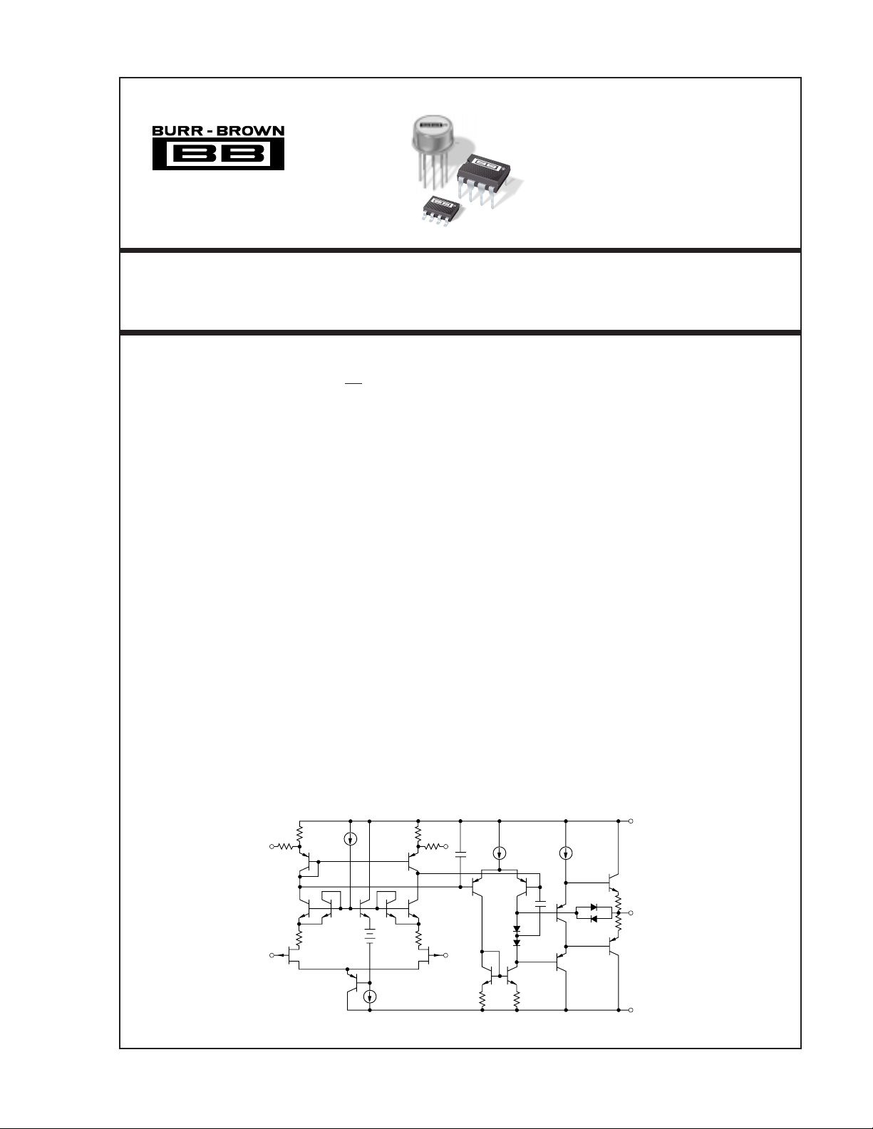
Difet
®
OPA627
OPA627
Precision High-Speed
®
OPERATIONAL AMPLIFIERS
OPA627
OPA637
FEATURES
● VERY LOW NOISE: 4.5nV/√Hz at 10kHz
● FAST SETTLING TIME:
OPA627—550ns to 0.01%
OPA637—450ns to 0.01%
● LOW V
● LOW DRIFT: 0.8
● LOW I
: 100µV max
OS
: 5pA max
B
µV/°C max
● OPA627: Unity-Gain Stable
● OPA637: Stable in Gain
≥ 5
DESCRIPTION
The OPA627 and OPA637
ers provide a new level of performance in a precision
FET op amp. When compared to the popular OPA111
op amp, the OPA627/637 has lower noise, lower offset
voltage, and much higher speed. It is useful in a broad
range of precision and high speed analog circuitry.
The OPA627/637 is fabricated on a high-speed, dielectrically-isolated complementary NPN/PNP process. It
operates over a wide range of power supply voltage—
±4.5V to ±18V. Laser-trimmed
provides high accuracy and low-noise performance
comparable with the best bipolar-input op amps.
Difet
operational amplifi-
Difet
input circuitry
APPLICATIONS
● PRECISION INSTRUMENTATION
● FAST DATA ACQUISITION
● DAC OUTPUT AMPLIFIER
● OPTOELECTRONICS
● SONAR, ULTRASOUND
● HIGH-IMPEDANCE SENSOR AMPS
● HIGH-PERFORMANCE AUDIO CIRCUITRY
● ACTIVE FILTERS
High frequency complementary transistors allow increased circuit bandwidth, attaining dynamic performance not possible with previous precision FET op
amps. The OPA627 is unity-gain stable. The OPA637
is stable in gains equal to or greater than five.
Difet
fabrication achieves extremely low input bias
currents without compromising input voltage noise
performance. Low input bias current is maintained
over a wide input common-mode voltage range with
unique cascode circuitry.
The OPA627/637 is available in plastic DIP, SOIC
and metal TO-99 packages. Industrial and military
temperature range models are available.
SBOS165
7
Trim
1
+In
3
®
Difet
, Burr-Brown Corp.
International Airport Industrial Park • Mailing Address: PO Box 11400, Tucson, AZ 85734 • Street Address: 6730 S. Tucson Blvd., Tucson, AZ 85706 • Tel: (520) 746-1111 • Twx: 910-952-1111
Internet: http://www.burr-brown.com/ • FAXLine: (800) 548-6133 (US/Canada Only) • Cable: BBRCORP • Telex: 066-6491 • FAX: (520) 889-1510 • Immediate Product Info: (800) 548-6132
©1989 Burr-Brown Corporation PDS-998H Printed in U.S.A. March, 1998
Trim
5
–In
2
+V
S
Output
6
–V
S
4
Page 2

SPECIFICATIONS
ELECTRICAL
At TA = +25°C, and VS = ±15V, unless otherwise noted.
OPA627BM, BP, SM OPA627AM, AP, AU
OPA637BM, BP, SM OPA637AM, AP, AU
PARAMETER CONDITIONS MIN TYP MAX MIN TYP MAX UNITS
OFFSET VOLTAGE
Input Offset Voltage 40 100 130 250 µV
AP, BP, AU Grades 100 250 280 500 µV
Average Drift 0.4 0.8 1.2 2 µV/°C
AP, BP, AU Grades 0.8 2 2.5 µV/°C
Power Supply Rejection VS = ±4.5 to ±18V 106 120 100 116 dB
INPUT BIAS CURRENT
Input Bias Current VCM = 0V 1 5 2 10 pA
Over Specified Temperature V
SM Grade V
Over Common-Mode Voltage V
Input Offset Current V
Over Specified Temperature V
SM Grade 50 nA
NOISE
Input Voltage Noise
Noise Density: f = 10Hz 15 40 20 nV/√Hz
Voltage Noise, BW = 0.1Hz to 10Hz 0.6 1.6 0.8 µVp-p
Input Bias Current Noise
Noise Density, f = 100Hz 1.6 2.5 2.5 fA/√Hz
Current Noise, BW = 0.1Hz to 10Hz 30 60 48 fAp-p
INPUT IMPEDANCE
Differential 10
Common-Mode 10
INPUT VOLTAGE RANGE
Common-Mode Input Range ±11 ±11.5 * * V
Over Specified Temperature ±10.5 ±11 * * V
Common-Mode Rejection V
OPEN-LOOP GAIN
Open-Loop Voltage Gain V
Over Specified Temperature V
SM Grade V
FREQUENCY RESPONSE
Slew Rate: OPA627 G = –1, 10V Step 40 55 * * V/µs
Settling Time: OPA627 0.01% G = –1, 10V Step 550 * ns
Gain-Bandwidth Product: OPA627 G = 1 16 * MHz
Total Harmonic Distortion + Noise G = +1, f = 1kHz 0.00003 * %
POWER SUPPLY
Specified Operating Voltage ±15 * V
Operating Voltage Range ±4.5 ±18 * * V
Current ±7 ±7.5 * * mA
OUTPUT
Voltage Output R
Over Specified Temperature ±11 ±11.5 * * V
Current Output V
Short-Circuit Current ±35 +70/–55 ±100***mA
Output Impedance, Open-Loop 1MHz 55 * Ω
TEMPERATURE RANGE
Specification: AP, BP, AM, BM, AU –25 +85 * * °C
Storage: AM, BM, SM –60 +150 * * °C
AP, BP, AU –40 +125 * * °C
θ
: AM, BM, SM 200 * ° C/W
J-A
AP, BP 100 * °C/W
AU 160 °C/W
* Specifications same as “B” grade.
NOTES: (1) Offset voltage measured fully warmed-up. (2) High-speed test at T
The information provided herein is believed to be reliable; however, BURR-BROWN assumes no responsibility for inaccuracies or omissions. BURR-BROWN assumes
no responsibility for the use of this information, and all use of such information shall be entirely at the user’s own risk. Prices and specifications are subject to change
without notice. No patent rights or licenses to any of the circuits described herein are implied or granted to any third party. BURR-BROWN does not authorize or warrant
any BURR-BROWN product for use in life support devices and/or systems.
(1)
(2)
= 0V 1 2 nA
CM
= 0V 50 nA
CM
= ±10V 1 2 pA
CM
= 0V 0.5 5 1 10 pA
CM
= 0V 1 2 nA
CM
f = 100Hz 8 20 10 nV/√Hz
f = 1kHz 5.2 8 5.6 nV/√Hz
f = 10kHz 4.5 6 4.8 nV/√Hz
13
|| 8 * Ω || pF
13
|| 7 * Ω || pF
= ±10.5V 106 116 100 110 dB
CM
= ±10V, RL = 1kΩ 112 120 106 116 dB
O
= ±10V, RL = 1kΩ 106 117 100 110 dB
O
= ±10V, RL = 1kΩ 100 114 dB
O
OPA637 G = –4, 10V Step 100 135 * * V/µs
0.1% G = –1, 10V Step 450 * ns
OPA637 0.01% G = –4, 10V Step 450 * ns
0.1% G = –4, 10V Step 300 * ns
OPA637 G = 10 80 * MHz
= 1kΩ±11.5 ±12.3 * *
L
= ±10V ±45 * mA
O
SM –55 +125 °C
= +25°C. See Typical Performance Curves for warmed-up performance.
J
®
OPA627, 637
2
Page 3
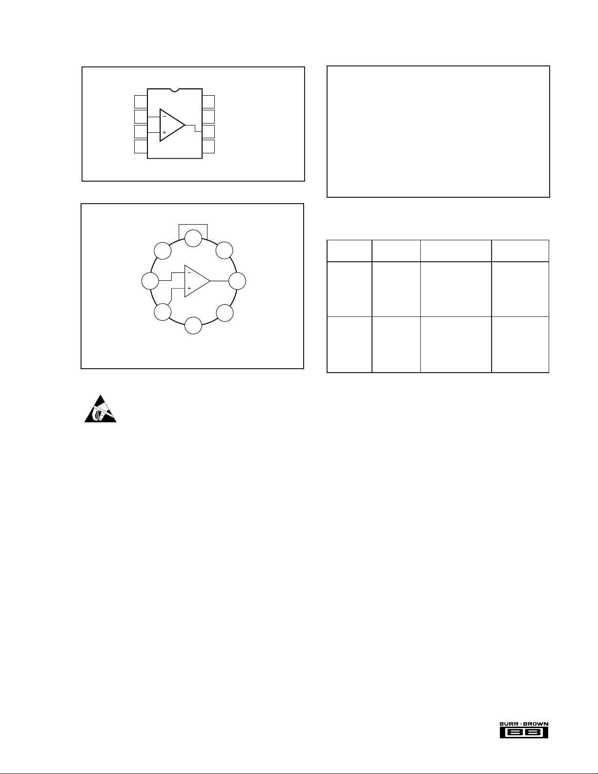
PIN CONFIGURATIONS
Top View
Offset Trim
Top View
Case connected to –V
1
–In
2
+In
3
–V
4
S
Offset Trim
–In
No Internal Connection
1
2
3
+In
.
S
ELECTROSTATIC
–V
8
No Internal Connection
7
+V
6
Output
5
Offset Trim
8
4
S
S
+V
7
6
5
Offset Trim
S
Output
DIP/SOIC
TO-99
ABSOLUTE MAXIMUM RATINGS
Supply Voltage .................................................................................. ±18V
Input Voltage Range .............................................. +V
Differential Input Range ....................................................... Total V
Power Dissipation ........................................................................ 1000mW
Operating Temperature
M Package .................................................................. –55°C to +125°C
P, U Package ............................................................. –40°C to +125°C
Storage Temperature
M Package .................................................................. –65°C to +150°C
P, U Package ............................................................. –40°C to +125°C
Junction Temperature
M Package .................................................................................. +175°C
P, U Package ............................................................................. +150°C
Lead Temperature (soldering, 10s)............................................... +300°C
SOlC (soldering, 3s) ................................................................... +260°C
NOTE: (1) Stresses above these ratings may cause permanent damage.
(1)
+ 2V to –VS – 2V
S
+ 4V
S
PACKAGE/ORDERING INFORMATION
PRODUCT PACKAGE NUMBER
PACKAGE DRAWING TEMPERATURE
OPA627AP Plastic DIP 006 –25°C to +85°C
OPA627BP Plastic DIP 006 –25°C to +85°C
OPA627AU SOIC 182 –25°C to +85°C
OPA627AM TO-99 Metal 001 –25°C to +85°C
OPA627BM TO-99 Metal 001 –25°C to +85°C
OPA627SM TO-99 Metal 001 –55°C to +125°C
OPA637AP Plastic DIP 006 –25°C to +85°C
OPA637BP Plastic DIP 006 –25°C to +85°C
OPA637AU SOIC 182 –25°C to +85°C
OPA637AM TO-99 Metal 001 –25°C to +85°C
OPA637BM TO-99 Metal 001 –25°C to +85°C
OPA637SM TO-99 Metal 001 –55°C to +125°C
NOTE: (1) For detailed drawing and dimension table, please see end of data
sheet, or Appendix C of Burr-Brown IC Data Book.
(1)
RANGE
DISCHARGE SENSITIVITY
This integrated circuit can be damaged by ESD. Burr-Brown
recommends that all integrated circuits be handled with
appropriate precautions. Failure to observe proper handling
and installation procedures can cause damage.
ESD damage can range from subtle performance degradation to complete device failure. Precision integrated circuits
may be more susceptible to damage because very small
parametric changes could cause the device not to meet its
published specifications.
®
3
OPA627, 637
Page 4

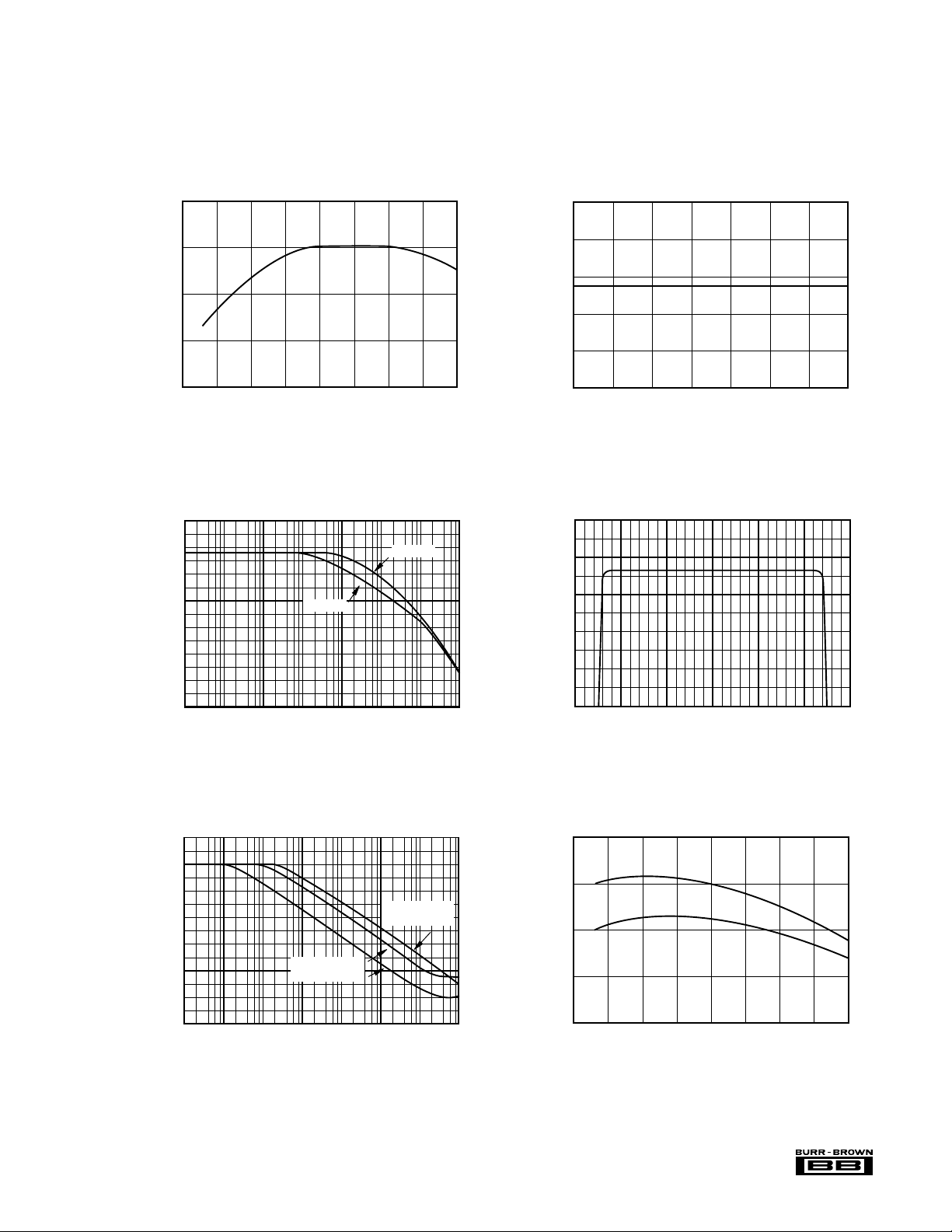
TYPICAL PERFORMANCE CURVES
At TA = +25°C, and VS = ±15V, unless otherwise noted.
INPUT VOLTAGE NOISE SPECTRAL DENSITY
1k
√
100
10
Voltage Noise (nV/ Hz)
1
1
10 100 1k 10k 100k 1M 10M
1k
√
100
10
Voltage Noise (nV/ Hz)
VOLTAGE NOISE vs SOURCE RESISTANCE
–
+
R
S
OPA627 + Resistor
1
100
1k 10k 100k 1M 10M 100M
Frequency (Hz)
Resistor Noise Only
Source Resistance ( )
Comparison with
OPA27 Bipolar Op
Amp + Resistor
Spot Noise
at 10kHz
Ω
TOTAL INPUT VOLTAGE NOISE vs BANDWIDTH
100
Noise Bandwidth:
0.1Hz to indicated
10
frequency.
1
0.1
Input Voltage Noise (µV)
0.01
1 10 100 1k 10k 100k 1M 10M
OPEN-LOOP GAIN vs FREQUENCY
140
120
100
80
60
40
Voltage Gain (dB)
20
0
–20
1 10 100 1k 10k 100k 1M 10M 100M
RMS
Bandwidth (Hz)
OPA627
Frequency (Hz)
p-p
OPA637
30
20
10
Gain (dB)
0
–10
OPA627 GAIN/PHASE vs FREQUENCY
1
®
OPA627, 637
Gain
Frequency (MHz)
75° Phase
Margin
10 100
Phase
–90
–120
–150
–180
–210
Gain (dB)
Phase (Degrees)
–10
4
30
20
10
0
1 10 100
OPA637 GAIN/PHASE vs FREQUENCY
Phase
Gain
Frequency (MHz)
–90
–120
–150
Phase (Degrees)
–180
–210
Page 5
TYPICAL PERFORMANCE CURVES (CONT)
OPEN-LOOP OUTPUT IMPEDANCE vs FREQUENCY
Frequency (Hz)
Output Resistance (Ω)
100
80
60
40
20
0
2 20 200 2k 20k 200k 2M 20M
POWER-SUPPLY REJECTION AND COMMON-MODE
REJECTION vs TEMPERATURE
Temperature (°C)
CMR and PSR (dB)
125
120
115
110
105
–75
PSR
CMR
–50 –25 0 25 50 75 100 125
At TA = +25°C, and VS = ±15V, unless otherwise noted.
125
120
115
Voltage Gain (dB)
110
105
–75 –50 –25 0 25 50 75 100 125
140
120
100
80
60
40
20
Common-Mode Rejection Ratio (dB)
0
OPEN-LOOP GAIN vs TEMPERATURE
Temperature (°C)
COMMON-MODE REJECTION vs FREQUENCY
OPA637
OPA627
1 10 100 1k 10k 100k 1M 10M
Frequency (Hz)
COMMON-MODE REJECTION vs
130
120
110
100
90
Common-Mode Rejection (dB)
80
–15 –10 –5 0 5 10 15
INPUT COMMON MODE VOLTAGE
Common-Mode Voltage (V)
140
120
100
Power-Supply Rejection (dB)
POWER-SUPPLY REJECTION vs FREQUENCY
80
60
40
20
0
1
10 100 1k 10k 100k 1M 10M
PSRR 627
+V
S
637
Frequency (Hz)
–VS PSRR 627
and 637
®
5
OPA627, 637
Page 6
TYPICAL PERFORMANCE CURVES (CONT)
At TA = +25°C, and VS = ±15V, unless otherwise noted.
8
SUPPLY CURRENT vs TEMPERATURE
7.5
7
Supply Current (mA)
6.5
6
–75 –50 –25 0 25 50 75 100 125
Temperature (°C)
OPA627 GAIN-BANDWIDTH AND SLEW RATE
vs TEMPERATURE
24
20
Slew Rate
16
12
Gain-Bandwidth (MHz)
GBW
60
55
Slew Rate (V/µs)
100
OUTPUT CURRENT LIMIT vs TEMPERATURE
80
+IL at VO = 0V
at VO = +10V
+I
L
60
40
at VO = 0V
–I
Output Current (mA)
20
L
–IL at VO = –10V
0
–75 –50 –25 0 25 50 75 100 125
Temperature (°C)
OPA637 GAIN-BANDWIDTH AND SLEW RATE
vs TEMPERATURE
120
Slew Rate
100
80
GBW
Gain-Bandwidth (MHz)
60
160
140
120
100
Slew Rate (V/µs)
8
0.1
0.01
0.001
THD+N (%)
0.0001
0.00001
–50 –25 0 25 50 75 100 125
–75
Temperature (°C)
OPA627 TOTAL HARMONIC DISTORTION + NOISE
vs FREQUENCY
G = +1 G = +10
V
+
I
–
V
V = ±10V
I
O
ΩΩ
100pF
V = ±10V
+
O
–
600600
5k
Ω
Ω
549
100pF
Measurement BW: 80kHz
G = +10
G = +1
20 100 1k 10k 20k
Frequency (Hz)
®
OPA627, 637
50
40
–50 –25 0 25 50 75 100 125
–75
80
Temperature (°C)
OPA637 TOTAL HARMONIC DISTORTION + NOISE
vs FREQUENCY
1
0.1
0.01
THD+N (%)
G = +10
V
+
I
V = ±10V
O
–
Ω
5k
549
Ω
Measurement BW: 80kHz
G = +50
V
+
I
600
Ω
100pF
V = ±10V
O
–
600
Ω
Ω
5k
102
Ω
100pF
G = +50
0.001
0.0001
G = +10
20 100 1k 10k 20k
Frequency (Hz)
6
Page 7

TYPICAL PERFORMANCE CURVES (CONT)
INPUT BIAS CURRENT
vs POWER SUPPLY VOLTAGE
Supply Voltage (±V
S
)
Input Bias Current (pA)
20
15
10
5
0
±4 ±6 ±8 ±10 ±12 ±14 ±16 ±18
NOTE: Measured fully
warmed-up.
TO-99 with 0807HS Heat Sink
TO-99
Plastic
DIP, SOIC
INPUT OFFSET VOLTAGE WARM-UP vs TIME
Time From Power Turn-On (Min)
Offset Voltage Change (µV)
50
25
0
–25
–50
0 1 2 3 4 5 6
At TA = +25°C, and VS = ±15V, unless otherwise noted.
INPUT BIAS AND OFFSET CURRENT
10k
1k
vs JUNCTION TEMPERATURE
100
10
Input Current (pA)
1
0.1
–50 –25 0 25 50 75 100 125 150
INPUT BIAS CURRENT vs COMMON-MODE VOLTAGE
1.2
1.1
1
0.9
Input Bias Current Multiplier
0.8
–15 –10 –5 0 5 10 15
Junction Temperature (°C)
Beyond Linear
Common-Mode Range
Common-Mode Voltage (V)
I
B
I
OS
Beyond Linear
Common-Mode Range
MAX OUTPUT VOLTAGE vs FREQUENCY
30
20
10
Output Voltage (Vp-p)
0
100k 1M 10M 100M
OPA627
OPA637
Frequency (Hz)
100
10
1
Settling Time (µs)
0.1
7
SETTLING TIME vs CLOSED-LOOP GAIN
Error Band: ±0.01%
OPA627
OPA637
–1 –10 –100 –1000
Closed-Loop Gain (V/V)
®
OPA627, 637
Page 8

TYPICAL PERFORMANCE CURVES (CONT)
At TA = +25°C, and VS = ±15V, unless otherwise noted.
1500
1000
500
Settling Time (ns)
0
0.001 0.01 0.1 1 10
SETTLING TIME vs ERROR BAND
C
F
R
F
2kΩ
+5V
–5V
OPA637
G = –4
R
I
–
+
Error Band (%)
OPA627 OPA637
R
2kΩ 500Ω
I
2kΩ 2kΩ
R
F
6pF 4pF
C
F
OPA627
G = –1
3
2
1
Settling Time (µs)
0
SETTLING TIME vs LOAD CAPACITANCE
Error Band:
±0.01%
0 150 200 300 400 500
Load Capacitance (pF)
OPA637
G = –4
OPA627
G = –1
APPLICATIONS INFORMATION
The OPA627 is unity-gain stable. The OPA637 may be used
to achieve higher speed and bandwidth in circuits with noise
gain greater than five. Noise gain refers to the closed-loop
gain of a circuit as if the non-inverting op amp input were
being driven. For example, the OPA637 may be used in a
non-inverting amplifier with gain greater than five, or an
inverting amplifier of gain greater than four.
When choosing between the OPA627 or OPA637, it is
important to consider the high frequency noise gain of your
circuit configuration. Circuits with a feedback capacitor
(Figure 1) place the op amp in unity noise-gain at high
frequency. These applications must use the OPA627 for
proper stability. An exception is the circuit in Figure 2,
where a small feedback capacitance is used to compensate
for the input capacitance at the op amp’s inverting input. In
this case, the closed-loop noise gain remains constant with
frequency, so if the closed-loop gain is equal to five or
greater, the OPA637 may be used.
®
OPA627, 637
RF < 4R
I
OPA627 OPA627
–
+
Buffer
OPA627
–
+
Bandwidth
Limiting
OPA627 OPA627
–
+
Integrator
R
–
+
Non-Inverting Amp
R
I
I
–
+
RF < 4R
OPA627
Inverting Amp
–
+
G < 5
G < |–4|
Filter
FIGURE 1. Circuits with Noise Gain Less than Five Require
the OPA627 for Proper Stability.
8
Page 9

OFFSET VOLTAGE ADJUSTMENT
–
+
2
3
In
Non-inverting
6
OPA627
Out
–
+
2
3
In
Inverting
6
OPA627
Out
–
+
2
3
In
Buffer
6
OPA627
Out
3
2
4
5
6
7
8 No Internal Connection
1
TO-99 Bottom View
To Guard Drive
The OPA627/637 is laser-trimmed for low offset voltage
and drift, so many circuits will not require external adjustment. Figure 3 shows the optional connection of an external
potentiometer to adjust offset voltage. This adjustment should
not be used to compensate for offsets created elsewhere in a
system (such as in later amplification stages or in an A/D
converter) because this could introduce excessive temperature drift. Generally, the offset drift will change by approximately 4µV/°C for 1mV of change in the offset voltage due
to an offset adjustment (as shown on Figure 3).
C
2
R
C
R
1
1
2
–
+
OPA637
C1 = CIN + C
C2 =
STRAY
R
1 C1
R
2
amp contributes little additional noise. Below 1kΩ, op amp
noise dominates over the resistor noise, but compares
favorably with precision bipolar op amps.
CIRCUIT LAYOUT
As with any high speed, wide bandwidth circuit, careful
layout will ensure best performance. Make short, direct
interconnections and avoid stray wiring capacitance—especially at the input pins and feedback circuitry.
The case (TO-99 metal package only) is internally connected
to the negative power supply as it is with most common op
amps. Pin 8 of the plastic DIP, SOIC, and TO-99 packages
has no internal connection.
Power supply connections should be bypassed with good
high frequency capacitors positioned close to the op amp
pins. In most cases 0.1µF ceramic capacitors are adequate.
The OPA627/637 is capable of high output current (in
excess of 45mA). Applications with low impedance loads or
capacitive loads with fast transient signals demand large
currents from the power supplies. Larger bypass capacitors
such as 1µF solid tantalum capacitors may improve dynamic
performance in these applications.
FIGURE 2. Circuits with Noise Gain Equal to or Greater than
Five May Use the OPA637.
NOISE PERFORMANCE
Some bipolar op amps may provide lower voltage noise
performance, but both voltage noise and bias current noise
contribute to the total noise of a system. The OPA627/637
is unique in providing very low voltage noise and very low
current noise. This provides optimum noise performance
over a wide range of sources, including reactive source
impedances. This can be seen in the performance curve
showing the noise of a source resistor combined with the
noise of an OPA627. Above a 2kΩ source resistance, the op
+V
S
100kΩ
7
2
–
3
+
–V
1
OPA627/637
4
S
5
10kΩ to 1MΩ
Potentiometer
(100kΩ preferred)
6
±10mV Typical
Trim Range
FIGURE 3. Optional Offset Voltage Trim Circuit.
Board Layout for Input Guarding:
Guard top and bottom of board.
Alternate—use Teflon
sitive input pins.
Teflon
FIGURE 4. Connection of Input Guard for Lowest IB.
®
E.I. du Pont de Nemours & Co.
®
standoff for sen-
®
9
OPA627, 637
Page 10

INPUT BIAS CURRENT
Difet
fabrication of the OPA627/637 provides very low
input bias current. Since the gate current of a FET doubles
approximately every 10°C, to achieve lowest input bias
current, the die temperature should be kept as low as possible. The high speed and therefore higher quiescent current
of the OPA627/637 can lead to higher chip temperature. A
simple press-on heat sink such as the Burr-Brown model
807HS (TO-99 metal package) can reduce chip temperature
by approximately 15°C, lowering the I
to one-third its
B
warmed-up value. The 807HS heat sink can also reduce lowfrequency voltage noise caused by air currents and thermoelectric effects. See the data sheet on the 807HS for details.
Temperature rise in the plastic DIP and SOIC packages can
be minimized by soldering the device to the circuit board.
Wide copper traces will also help dissipate heat.
The OPA627/637 may also be operated at reduced power
supply voltage to minimize power dissipation and temperature rise. Using ±5V power supplies reduces power dissipation to one-third of that at ±15V. This reduces the I
of TO-
B
99 metal package devices to approximately one-fourth the
value at ±15V.
Leakage currents between printed circuit board traces can
easily exceed the input bias current of the OPA627/637. A
circuit board “guard” pattern (Figure 4) reduces leakage
effects. By surrounding critical high impedance input circuitry with a low impedance circuit connection at the same
potential, leakage current will flow harmlessly to the lowimpedance node. The case (TO-99 metal package only) is
internally connected to –V
.
S
Input bias current may also be degraded by improper handling or cleaning. Contamination from handling parts and
circuit boards may be removed with cleaning solvents and
deionized water. Each rinsing operation should be followed
by a 30-minute bake at 85°C.
Many FET-input op amps exhibit large changes in input
bias current with changes in input voltage. Input stage
cascode circuitry makes the input bias current of the
OPA627/637 virtually constant with wide common-mode
voltage changes. This is ideal for accurate high inputimpedance buffer applications.
PHASE-REVERSAL PROTECTION
The OPA627/637 has internal phase-reversal protection.
Many FET-input op amps exhibit a phase reversal when the
input is driven beyond its linear common-mode range. This
is most often encountered in non-inverting circuits when the
input is driven below –12V, causing the output to reverse
into the positive rail. The input circuitry of the OPA627/637
does not induce phase reversal with excessive commonmode voltage, so the output limits into the appropriate rail.
OUTPUT OVERLOAD
When the inputs to the OPA627/637 are overdriven, the
output voltage of the OPA627/637 smoothly limits at approximately 2.5V from the positive and negative power
supplies. If driven to the negative swing limit, recovery
takes approximately 500ns. When the output is driven into
the positive limit, recovery takes approximately 6µs. Output
recovery of the OPA627 can be improved using the output
clamp circuit shown in Figure 5. Diodes at the inverting
input prevent degradation of input bias current.
+V
S
–V
5kΩ
ZD
5kΩ
S
Diode Bridge
1
BB: PWS740-3
ZD : 10V IN961
1
V
O
Clamps output
= ±11.5V
at V
O
(2)
HP 5082-2811
1kΩ
R
V
I
R
I
–
+
F
OPA627
FIGURE 5. Clamp Circuit for Improved Overload Recovery.
CAPACITIVE LOADS
As with any high-speed op amp, best dynamic performance
can be achieved by minimizing the capacitive load. Since a
load capacitance presents a decreasing impedance at higher
frequency, a load capacitance which is easily driven by a
slow op amp can cause a high-speed op amp to perform
poorly. See the typical curves showing settling times as a
function of capacitive load. The lower bandwidth of the
OPA627 makes it the better choice for driving large capacitive loads. Figure 6 shows a circuit for driving very large
load capacitance. This circuit’s two-pole response can also
be used to sharply limit system bandwidth. This is often
useful in reducing the noise of systems which do not require
the full bandwidth of the OPA627.
R
F
1kΩ
200pF
G = +1
BW 1MHz
C
L
5nF
O
≥
R
G = 1+
R
Optional Gain
Gain > 1
C
F
R
F
–3dB
O
20Ω
2 R
O CL
RF
2π √ R
RF >> R
1
F RO CF CL
=
=
–
+
F
1
OPA627
R
1
For Approximate Butterworth Response:
C
f
FIGURE 6. Driving Large Capacitive Loads.
®
OPA627, 637
10
Page 11

INPUT PROTECTION
The inputs of the OPA627/637 are protected for voltages
between +V
+ 2V and –VS – 2V. If the input voltage can
S
exceed these limits, the amplifier should be protected. The
diode clamps shown in Figure 7a will prevent the input
voltage from exceeding one forward diode voltage drop
beyond the power supplies—well within the safe limits. If
the input source can deliver current in excess of the maximum forward current of the protection diodes, use a series
resistor, R
, to limit the current. Be aware that adding
S
resistance to the input will increase noise. The 4nV/√Hz
theoretical thermal noise of a 1kΩ resistor will add to the
4.5nV/√Hz noise of the OPA627/637 (by the square-root of
the sum of the squares), producing a total noise of 6nV/√Hz.
Resistors below 100Ω add negligible noise.
Leakage current in the protection diodes can increase the
total input bias current of the circuit. The specified maximum leakage current for commonly used diodes such as the
1N4148 is approximately 25nA—more than a thousand
times larger than the input bias current of the OPA627/637.
Leakage current of these diodes is typically much lower and
may be adequate in many applications. Light falling on the
junction of the protection diodes can dramatically increase
leakage current, so common glass-packaged diodes should
be shielded from ambient light. Very low leakage can be
achieved by using a diode-connected FET as shown. The
2N4117A is specified at 1pA and its metal case shields the
junction from light.
Sometimes input protection is required on I/V converters of
inverting amplifiers (Figure 7b). Although in normal operation, the voltage at the summing junction will be near zero
(equal to the offset voltage of the amplifier), large input
transients may cause this node to exceed 2V beyond the
power supplies. In this case, the summing junction should
be protected with diode clamps connected to ground. Even
with the low voltage present at the summing junction,
common signal diodes may have excessive leakage current.
Since the reverse voltage on these diodes is clamped, a
diode-connected signal transistor can be used as an inexpensive low leakage diode (Figure 7b).
+V
S
Optional R
(a)
I
IN
D
(b)
D
D
S
–V
S
D
–
+
OPA627
D: IN4148 — 25nA Leakage
2N4117A — 1pA Leakage
–
+
OPA627
D: 2N3904
V
O
Siliconix
=
V
=
O
LARGE SIGNAL RESPONSE
(A) (B)
FPO
When used as a unity-gain buffer, large common-mode input voltage steps
produce transient variations in input-stage currents. This causes the rising
edge to be slower and falling edges to be faster than nominal slew rates
observed in higher-gain circuits.
FIGURE 8. OPA627 Dynamic Performance, G = +1.
FIGURE 7. Input Protection Circuits.
SMALL SIGNAL RESPONSE
–
+
OPA627
NC
G = 1
11
®
OPA627, 637
Page 12

LARGE SIGNAL RESPONSE
+10
(V)
0
OUT
V
–10
When driven with a very fast input step (left), common-mode
transients cause a slight variation in input stage currents which
will reduce output slew rate. If the input step slew rate is reduced
(right), output slew rate will increase slightly.
(C) (D)
FIGURE 9. OPA627 Dynamic Performance, G = –1.
LARGE SIGNAL RESPONSE
OPA637
+10
(V)
0
OUT
V
–10
NOTE: (1) Optimum value will
depend on circuit board layout and stray capacitance at
the inverting input.
SMALL SIGNAL RESPONSE
2kΩ
OPA637
6pF
2kΩ
–
+
(1)
OPA627
G = –1
V
OUT
+10
(V)
0
OUT
V
–10
FIGURE 10. OPA637 Dynamic Response, G = 5.
500Ω
4pF
2kΩ
–
+
(1)
OPA637
+100
(mV)
0
OUT
V
–100
G = 5
V
OUT
NOTE: (1) Optimum value will depend on circuit
board layout and capacitance at inverting input.
FPO
(F)(E)
®
OPA627, 637
12
Page 13

/
R
I
2kΩ
Error Out
C
F
HP5082-
2kΩ
2835
+15V
R
51Ω
I
–
+
±5V
Out
High Quality
Pulse Generator
–15V
FIGURE 11. Settling Time and Slew Rate Test Circuit.
R
101Ω
G
+
–
–
+
OPA637
R
F
5kΩ
3pF
R
F
5kΩ
OPA637
Differential Voltage Gain = 1 + 2R
–In
Input Common-Mode
Range = ±5V
+In
FIGURE 12. High Speed Instrumentation Amplifier, Gain = 100.
OPA627 OPA637
, R
R
I
1
C
F
Error Band ±0.5mV ±0.2mV
2kΩ 500Ω
6pF 4pF
(0.01%)
NOTE: CF is selected for best settling time performance
depending on test fixture layout. Once optimum value is
determined, a fixed capacitor may be used.
Gain = 100
≈
CMRR 116dB
Bandwidth 1MHz
2
25kΩ
≈
25kΩ
5
INA105
3
Differential
Amplifier
25kΩ
–
+
25kΩ
Output
6
1
F/RG
–In
+
–
OPA637
R
F
5kΩ
Input Common-Mode
Range = ±10V
+In
R
101Ω
G
–
+
3pF
R
F
5kΩ
OPA637
Differential Voltage Gain = (1 + 2R
FIGURE 13. High Speed Instrumentation Amplifier, Gain = 1000.
R
2
–
A
V
I
1
+
R
1
R
+
V
–
OPA603
*
3
R
4
O
RL ≥ 150Ω
for ±10V Out
GAIN A
(V/V) OP AMP (Ω )(kΩ)(Ω)(kΩ) (MHz) (V/
100 OPA627 50.5
1000 OPA637 49.9 4.99 12 1 11 500
NOTE: (1) Closest 1/2% value.
FIGURE 14. Composite Amplifier for Wide Bandwidth.
Gain = 1000
≈
CMRR 116dB
Bandwidth 400kHz
2
10kΩ
≈
100kΩ
5
INA106
3
Differential
Amplifier
10kΩ
–
+
100kΩ
Output
6
1
) • 10
F/RG
This composite amplifier uses the OPA603 current-feedback op amp to
provide extended bandwidth and slew rate at high closed-loop gain. The
feedback loop is closed around the composite amp, preserving the
precision input characteristics of the OPA627/637. Use separate power
supply bypass capacitors for each op amp.
*Minimize capacitance at this node.
R1R2R3R4–3dB SLEW RATE
1
(1)
4.99 20 1 15 700
µs)
13
®
OPA627, 637
Page 14

PACKAGE OPTION ADDENDUM
www.ti.com
PACKAGING INFORMATION
Orderable Device Status
OPA627AM NRND TO-99 LMC 8 20 Green (RoHS&
OPA627AP ACTIVE PDIP P 8 50 Green (RoHS&
OPA627APG4 ACTIVE PDIP P 8 50 Green (RoHS&
OPA627AU ACTIVE SOIC D 8 100 Green (RoHS &
OPA627AU/2K5 ACTIVE SOIC D 8 2500 Green (RoHS &
OPA627AU/2K5E4 ACTIVE SOIC D 8 2500 Green (RoHS &
OPA627AUE4 ACTIVE SOIC D 8 100 Pb-Free
OPA627AUG4 ACTIVE SOIC D 8 100 Green (RoHS &
OPA627BM NRND TO-99 LMC 8 20 Green (RoHS&
OPA627BP ACTIVE PDIP P 8 50 Green (RoHS&
OPA627BPG4 ACTIVE PDIP P 8 50 Green (RoHS&
OPA627SM NRND TO-99 LMC 8 20 Green (RoHS&
OPA637AM NRND TO-99 LMC 8 20 Green (RoHS&
OPA637AM2 OBSOLETE TO-99 LMC 8 TBD Call TI Call TI
OPA637AP ACTIVE PDIP P 8 50 Green (RoHS&
OPA637APG4 ACTIVE PDIP P 8 50 Green (RoHS&
OPA637AU ACTIVE SOIC D 8 100 Green (RoHS &
OPA637AU/2K5 ACTIVE SOIC D 8 2500 Green (RoHS &
OPA637AU/2K5E4 ACTIVE SOIC D 8 2500 Green (RoHS &
OPA637AUE4 ACTIVE SOIC D 8 100 TBD Call TI Call TI
OPA637AUG4 ACTIVE SOIC D 8 100 Green (RoHS &
OPA637BM NRND TO-99 LMC 8 20 Green (RoHS&
OPA637BM1 OBSOLETE TO-99 LMC 8 TBD Call TI Call TI
OPA637BP ACTIVE PDIP P 8 50 Green (RoHS&
OPA637BPG4 ACTIVE PDIP P 8 50 Green (RoHS&
OPA637SM NRND TO-99 LMC 8 20 Green (RoHS&
(1)
Package
Type
Package
Drawing
Pins Package
Qty
Eco Plan
no Sb/Br)
no Sb/Br)
no Sb/Br)
no Sb/Br)
no Sb/Br)
no Sb/Br)
no Sb/Br)
no Sb/Br)
no Sb/Br)
no Sb/Br)
no Sb/Br)
no Sb/Br)
no Sb/Br)
no Sb/Br)
no Sb/Br)
no Sb/Br)
no Sb/Br)
no Sb/Br)
no Sb/Br)
no Sb/Br)
no Sb/Br)
no Sb/Br)
(RoHS)
(2)
Lead/Ball Finish MSL Peak Temp
AU N / Afor Pkg Type
CU NIPDAU N / A for PkgType
CU NIPDAU N / A for PkgType
CU NIPDAU Level-3-260C-168 HR
CU NIPDAU Level-3-260C-168 HR
CU NIPDAU Level-3-260C-168 HR
CU NIPDAU Level-3-260C-168 HR
CU NIPDAU Level-3-260C-168 HR
AU N / Afor Pkg Type
CU NIPDAU N / A for PkgType
CU NIPDAU N / A for PkgType
AU N / Afor Pkg Type
AU N / Afor Pkg Type
CU NIPDAU N / A for PkgType
CU NIPDAU N / A for PkgType
CU NIPDAU Level-3-260C-168 HR
CU NIPDAU Level-3-260C-168 HR
CU NIPDAU Level-3-260C-168 HR
CU NIPDAU Level-3-260C-168 HR
AU N / Afor Pkg Type
CU NIPDAU N / A for PkgType
CU NIPDAU N / A for PkgType
AU N / Afor Pkg Type
19-Dec-2007
(3)
Addendum-Page 1
Page 15

PACKAGE OPTION ADDENDUM
www.ti.com
(1)
The marketing status values are defined as follows:
19-Dec-2007
ACTIVE: Product device recommended for new designs.
LIFEBUY: TI has announced that the device will be discontinued, and a lifetime-buy period is in effect.
NRND: Not recommended for new designs. Device is in production to support existing customers, but TI does not recommend using this part in
a new design.
PREVIEW: Device has been announced but is not in production. Samples may or may not be available.
OBSOLETE: TI has discontinued the production of the device.
(2)
Eco Plan - The planned eco-friendly classification: Pb-Free (RoHS), Pb-Free (RoHS Exempt), or Green (RoHS & no Sb/Br) - please check
http://www.ti.com/productcontent for the latest availability information and additional product content details.
TBD: The Pb-Free/Green conversion plan has not been defined.
Pb-Free (RoHS): TI's terms "Lead-Free" or "Pb-Free" mean semiconductor products that are compatible with the current RoHS requirements
for all 6 substances, including the requirement that lead not exceed 0.1% by weight in homogeneous materials. Where designed to be soldered
at high temperatures, TI Pb-Free products are suitable for use in specified lead-free processes.
Pb-Free (RoHS Exempt): This component has a RoHS exemption for either 1) lead-based flip-chip solder bumps used between the die and
package, or 2) lead-based die adhesive used between the die and leadframe. The component is otherwise considered Pb-Free (RoHS
compatible) as defined above.
Green (RoHS & no Sb/Br): TI defines "Green" to mean Pb-Free (RoHS compatible), and free of Bromine (Br) and Antimony (Sb) based flame
retardants (Br or Sb do not exceed 0.1% by weight in homogeneous material)
(3)
MSL, Peak Temp. -- The Moisture Sensitivity Level rating according to the JEDEC industry standard classifications, and peak solder
temperature.
Important Information and Disclaimer:The information provided on this page represents TI's knowledge and belief as of the date that it is
provided. TI bases its knowledge and belief on information provided by third parties, and makes no representation or warranty as to the
accuracy of such information. Efforts are underway to better integrate information from third parties. TI has taken and continues to take
reasonable steps to provide representative and accurate information but may not have conducted destructive testing or chemical analysis on
incoming materials and chemicals. TI and TI suppliers consider certain information to be proprietary, and thus CAS numbers and other limited
information may not be available for release.
In no event shall TI's liability arising out of such information exceed the total purchase price of the TI part(s) at issue in this document sold by TI
to Customer on an annual basis.
Addendum-Page 2
Page 16

PACKAGE MATERIALS INFORMATION
www.ti.com
TAPE AND REEL INFORMATION
11-Mar-2008
*All dimensionsare nominal
Device Package
OPA627AU/2K5 SOIC D 8 2500 330.0 12.4 6.4 5.2 2.1 8.0 12.0 Q1
Type
Package
Drawing
Pins SPQ Reel
Diameter
(mm)
Reel
Width
W1 (mm)
A0 (mm) B0 (mm) K0 (mm) P1
(mm)W(mm)
Pin1
Quadrant
Pack Materials-Page 1
Page 17

PACKAGE MATERIALS INFORMATION
www.ti.com
11-Mar-2008
*All dimensionsare nominal
Device Package Type Package Drawing Pins SPQ Length (mm) Width (mm) Height (mm)
OPA627AU/2K5 SOIC D 8 2500 346.0 346.0 29.0
Pack Materials-Page 2
Page 18

IMPORTANT NOTICE
Texas Instruments Incorporated and its subsidiaries (TI) reserve the right to make corrections, modifications, enhancements, improvements,
and other changes to its products and services at any time and to discontinue any product or service without notice. Customers should
obtain the latest relevant information before placing orders and should verify that such information is current and complete. All products are
sold subject to TI’s terms and conditions of sale supplied at the time of order acknowledgment.
TI warrants performance of its hardware products to the specifications applicable at the time of sale in accordance with TI’s standard
warranty. Testing and other quality control techniques are used to the extent TI deems necessary to support this warranty. Except where
mandated by government requirements, testing of all parameters of each product is not necessarily performed.
TI assumes no liability for applications assistance or customer product design. Customers are responsible for their products and
applications using TI components. To minimize the risks associated with customer products and applications, customers should provide
adequate design and operating safeguards.
TI does not warrant or represent that any license, either express or implied, is granted under any TI patent right, copyright, mask work right,
or other TI intellectual property right relating to any combination, machine, or process in which TI products or services are used. Information
published by TI regarding third-party products or services does not constitute a license from TI to use such products or services or a
warranty or endorsement thereof. Use of such information may require a license from a third party under the patents or other intellectual
property of the third party, or a license from TI under the patents or other intellectual property of TI.
Reproduction of TI information in TI data books or data sheets is permissible only if reproduction is without alteration and is accompanied
by all associated warranties, conditions, limitations, and notices. Reproduction of this information with alteration is an unfair and deceptive
business practice. TI is not responsible or liable for such altered documentation. Information of third parties may be subject to additional
restrictions.
Resale of TI products or services with statements different from or beyond the parameters stated by TI for that product or service voids all
express and any implied warranties for the associated TI product or service and is an unfair and deceptive business practice. TI is not
responsible or liable for any such statements.
TI products are not authorized for use in safety-critical applications (such as life support) where a failure of the TI product would reasonably
be expected to cause severe personal injury or death, unless officers of the parties have executed an agreement specifically governing
such use. Buyers represent that they have all necessary expertise in the safety and regulatory ramifications of their applications, and
acknowledge and agree that they are solely responsible for all legal, regulatory and safety-related requirements concerning their products
and any use of TI products in such safety-critical applications, notwithstanding any applications-related information or support that may be
provided by TI. Further, Buyers must fully indemnify TI and its representatives against any damages arising out of the use of TI products in
such safety-critical applications.
TI products are neither designed nor intended for use in military/aerospace applications or environments unless the TI products are
specifically designated by TI as military-grade or "enhanced plastic." Only products designated by TI as military-grade meet military
specifications. Buyers acknowledge and agree that any such use of TI products which TI has not designated as military-grade is solely at
the Buyer's risk, and that they are solely responsible for compliance with all legal and regulatory requirements in connection with such use.
TI products are neither designed nor intended for use in automotive applications or environments unless the specific TI products are
designated by TI as compliant with ISO/TS 16949 requirements. Buyers acknowledge and agree that, if they use any non-designated
products in automotive applications, TI will not be responsible for any failure to meet such requirements.
Following are URLs where you can obtain information on other Texas Instruments products and application solutions:
Products Applications
Amplifiers amplifier.ti.com Audio www.ti.com/audio
Data Converters dataconverter.ti.com Automotive www.ti.com/automotive
DSP dsp.ti.com Broadband www.ti.com/broadband
Clocks and Timers www.ti.com/clocks Digital Control www.ti.com/digitalcontrol
Interface interface.ti.com Medical www.ti.com/medical
Logic logic.ti.com Military www.ti.com/military
Power Mgmt power.ti.com Optical Networking www.ti.com/opticalnetwork
Microcontrollers microcontroller.ti.com Security www.ti.com/security
RFID www.ti-rfid.com Telephony www.ti.com/telephony
RF/IF and ZigBee® Solutions www.ti.com/lprf Video & Imaging www.ti.com/video
Mailing Address: Texas Instruments, Post Office Box 655303, Dallas, Texas 75265
Copyright © 2008, Texas Instruments Incorporated
Wireless www.ti.com/wireless
 Loading...