

Page 1
User's Guide
SBOU219–February 2020
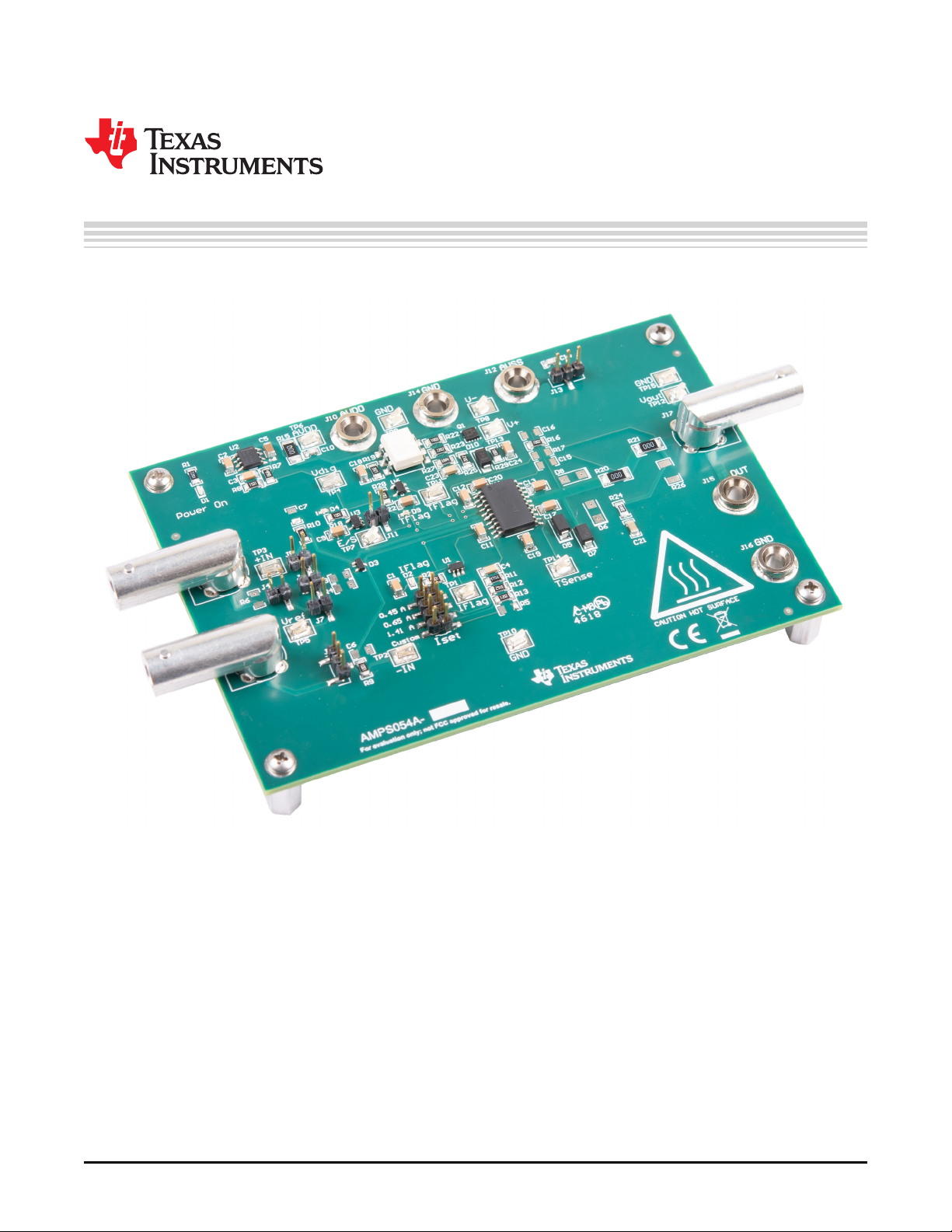
OPA564DWP-EVM
This user’s guide describes the design, operation, and use cases of the OPA564 evaluation module
(EVM) for the DWP package only; this EVM cannot be used with the OPA564 DWD package. This guide
discusses how to set up and configure the board hardware, and describes five different applications this
evaluation module can be used for. Throughout this document, the terms evaluation module, EVM, or
simply board are synonymous with the OPA564DWP-EVM. This document also includes an electrical
schematic, a printed circuit board (PCB) layout drawing, and a parts list for this EVM.
1 Overview...................................................................................................................... 3
1.1 OPA564 Overview .................................................................................................. 3
1.2 General Overview of the OPA564DWP-EVM................................................................... 3
1.3 Related Documentation from Texas Instruments............................................................... 4
2 Hardware...................................................................................................................... 5
2.1 Power Supply........................................................................................................ 5
2.2 Inputs................................................................................................................. 5
2.3 Outputs............................................................................................................... 5
2.4 Jumpers.............................................................................................................. 6
SBOU219–February 2020
Submit Documentation Feedback
Contents
Copyright © 2020, Texas Instruments Incorporated
OPA564DWP-EVM
1
Page 2

www.ti.com
2.5 LEDs.................................................................................................................. 6
2.6 Enable-Disable Feature............................................................................................ 6
2.7 Current Limitation Capability ...................................................................................... 6
3 Configuration Examples..................................................................................................... 7
3.1 Noninverting Amplifier Configuration Setup ..................................................................... 7
3.2 Inverting Amplifier Configuration Setup .......................................................................... 9
3.3 Differential Amplifier Configuration Setup...................................................................... 11
3.4 Improved Howland Current Pump Configuration Setup...................................................... 13
3.5 Bridge-Tied Load Configuration Setup ........................................................................ 15
4 Schematics, PCB Layout, and Bill of Materials......................................................................... 17
4.1 Schematics......................................................................................................... 17
4.2 PCB Layout ........................................................................................................ 18
4.3 Bill of Materials .................................................................................................... 21
List of Figures
1 Noninverting Amplifier Configuration Schematic ........................................................................ 7
2 Noninverting Operation ..................................................................................................... 8
3 Inverting Amplifier Configuration Schematic ............................................................................. 9
4 Inverting Operation......................................................................................................... 10
5 Differential Amplifier Configuration Schematic ......................................................................... 11
6 Differential Operation ...................................................................................................... 12
7 Improved Howland Current Pump Schematic .......................................................................... 13
8 Bridge-Tied Load Schematic.............................................................................................. 15
9 Bridge-Tied Load Operation .............................................................................................. 16
10 OPA564DWP-EVM Schematic .......................................................................................... 17
11 OPA564DWP-EVM, Top Layer .......................................................................................... 19
12 OPA564DWP-EVM Bottom Layer ....................................................................................... 20
1 Related Documentation ..................................................................................................... 4
2 Basic Jumper Functions .................................................................................................... 6
3 Status of the LEDs........................................................................................................... 6
4 Noninverting Configuration ................................................................................................. 7
5 Inverting Configuration ...................................................................................................... 9
6 Differential Configuration .................................................................................................. 11
7 Improved Howland Current Pump Configuration....................................................................... 13
8 Bridge-Tied Load Configuration: Board 1 ............................................................................... 15
9 Bridge-Tied Load Configuration: Board 2 ............................................................................... 16
10 Bill of Materials ............................................................................................................. 21
Trademarks
PowerPAD is a trademark of Texas Instruments.
All other trademarks are the property of their respective owners.
List of Tables
2
OPA564DWP-EVM
Copyright © 2020, Texas Instruments Incorporated
SBOU219–February 2020
Submit Documentation Feedback
Page 3

www.ti.com
1 Overview
1.1 OPA564 Overview
The OPA564 is a low-cost, high-current, operational amplifier (op amp) capable of providing up to 1.5 A of
current to an output load. The high slew rate of this op amp provides 1.3-MHz, full-power bandwidth and
excellent linearity. This monolithic integrated circuit provides high reliability in demanding powerline
communications and motor-control applications.
1.1.1 OPA564 Safety Considerations
The OPA564 op amps can use a power-supply voltage as great as 24 V in single-supply connection, or
±12 V in dual-supply connection, both of which represent a potential difference of 24 V. The possibility for
accidental electrical shock increases with the increased potential difference and the user must take
precautions to avoid contact with the PCB when live voltage is present. If circuit probing is required and
voltages are present, best practice is to apply the one hand rule. Use an insulated probe and only one
hand when probing the live circuit. Keep the other hand away from the circuit and any metal contacts in
the immediate area through that current can flow.
Power op amps can generate a lot of heat under certain operating conditions. This excess heat must be
conducted away from the amplifier in order to maintain correct operation and long life. The DWP package
contains the PowerPAD™ heat sink located on the bottom for this purpose. Still, the device under test
(DUT) might grow hot during the test; therefore, avoid contact with the DUT when the circuit is in use, or
during cool down after use.
Overview
1.2 General Overview of the OPA564DWP-EVM
This DWP package-specific OPA564 evaluation module (EVM), allows users to easily evaluate design
concepts. This EVM is easily configured as a noninverting, inverting, or difference amplifier, as an
improved Howland current pump, or as a BTL (bridge tied load) circuit. BTL requires two EVMs used
concurrently to create this circuit configuration, however. This guide discusses all individual circuit
configurations and hardware setup associated.
This EVM is based on a 5.0-inch × 3.5-inch (12.7-cm × 8.9-cm) PCB that accommodates the 20-lead,
DWP powerPAD package. This EVM cannot be used with the OPA564 DWD package.
The OPA564 can be operated with either a single supply (V+ and ground), or dual supplies (V+ and V–);
therefore, the EVM is designed to be used in either mode. A jumper (J13) sets the supply condition. The
enable-shutdown function and thermal shutdown indicator are functional with either supply arrangement;
shutdown mode is a low current, output disabled mode.
Three LEDs (green, orange, and red) indicate EVM functionality. A green LED (D1) illuminates when V+ is
applied. A red LED (D9) illuminates when the amplifier is in thermal shutdown mode (for approximately 10
µs or longer), and both the red and orange LED (D4) illuminate when the amplifier is set to shutdown
mode (through jumper J11). During normal operation, the yellow and red LEDs are off.
1.2.1 Supply Voltage Considerations for the OPA564DWP-EVM
The OPA564DWP-EVM is designed to be powered by the user’s single or dual, high-current, high-voltage
power supply. In dual-supply configuration, set the minimum V+ and V– levels at ±3.5 V. In single powersupply mode, use a minimum of V+ = 7 V for correct functionality. Do not exceed the maximum supply
voltage of 24 V in single-supply mode (V+), or ±12 V in dual-supply mode.
If required, disable the OPA564 by placing a shunt on jumper J11.
SBOU219–February 2020
Submit Documentation Feedback
Copyright © 2020, Texas Instruments Incorporated
OPA564DWP-EVM
3
Page 4

Overview
1.3 Related Documentation from Texas Instruments
This user's guide is available from the TI web site under literature number SBOU219. Any letter appended
to the literature number corresponds to the document revision that is current at the time of the writing of
this document. Newer revisions may be available from the TI web site, or call the Texas Instruments'
Literature Response Center at (800) 477-8924 or the Product Information Center at (972) 644-5580. When
ordering, please identify the document by both title and literature number.
Table 1 gives links to the OPA564 data sheet, and an in-depth Howland current pump application note.
Table 1. Related Documentation
Document Literature Number
OPA564 product data sheet SBOS372
AN-1515 A Comprehensive Study of the Howland Current Pump application note SNOA474
www.ti.com
4
OPA564DWP-EVM
Copyright © 2020, Texas Instruments Incorporated
SBOU219–February 2020
Submit Documentation Feedback
Page 5

www.ti.com
2 Hardware
This section details the purpose of the EVM connectors and jumpers, and methods of configuring the EVM
for taking measurements.
See Section 4 for the OPA564DWP-EVM schematic.
2.1 Power Supply
Power is provided to the OPA564DWP-EVM through three banana jacks: AVDD (V+), GND, and AVSS
(V–). The EVM can be configured to use a single 7-V to 24-V supply (by placing a shunt on the right-hand
side of J13, thus connecting V– to GND), or a dual ±3.5-V to ±12-V supply (by placing a shunt on the lefthand side of J13, thus connecting V– to AVSS). Use a power supply that is capable of providing at least
2× the anticipated continuous current to account for peak current conditions. Furthermore, make certain
that any cables used to carry high current are rated for such use.
2.2 Inputs
The input to the EVM may be a dc signal, an ac signal (such as that from a signal generator), or any other
signal within the common-mode voltage range. Be aware that 50-Ω termination resistors are not installed
at the EVM inputs. If necessary, external, higher-wattage BNC terminators can be added at the EVM input
connectors. Excessive power dissipation, under high input voltage conditions, can result in potential failure
of the device.
The signal presented to the inverting OPA564 input pin (Vin–) is selected through jumper J3. Vin– can be
set to GND by placing a shunt on the upper portion of J3, or a signal applied at the BNC input connector
J2 by placing a shunt on the lower portion of J3.
The signal presented to the noninverting input (Vin+) can be adjusted as follows:
• Place a shunt on J4 to connect Vin+ to a signal applied at the BNC input connector J1.
• Place a shunt on J5 to set Vin+ to GND.
• Place a shunt on J6 to set Vin+ to a voltage value midway between the two supplies.
• Place a shunt on J7 to set Vin+ to an externally set voltage (through TP5), or to offset the input voltage
by the externally set reference voltage value.
• Place a shunt on J9 to reference Vin+ to ground through a 10-kΩ resistor. This setting is necessary for
correct difference amplifier operation.
Hardware
2.3 Outputs
Output signals derived from the EVM can be monitored in a number of ways. The OPA564DWP-EVM can
be accessed through a BNC connector (J17), intended for an instrument connection (an oscilloscope, for
example) , or a pair of female banana jacks (J15, J16), intended for carrying high output current.
The OPA564 can drive a variety of loads, some of which may be large or have to dissipate a significant
amount of power. Therefore, an external load can be applied to the OPA564DWP-EVM for high-power
applications. Alternatively, for low-power applications, a load resistor can be added through the R26
footprint.
SBOU219–February 2020
Submit Documentation Feedback
Copyright © 2020, Texas Instruments Incorporated
OPA564DWP-EVM
5
Page 6
lim
1.2 V
R5 5 k
:
Hardware
2.4 Jumpers
A description of basic jumper functions is shown in Table 2. More information can be found in Section 2.
Jumper Description
J3 Selects the signal presented to the amplifier Vin– pin
J4, J5, J6 Selects the signal presented to the amplifier Vin+ pin
J7 Selects the reference voltage to the amplifier positive input (external Vref)
J8 Selects the current limit for OPA564
J9 Allows the user to reference the noninverting input to ground via a 10-kΩ resistor. Used in difference
J11 Disables or enables the OPA564 output
J13 Allows the user to select single or dual power-supply mode
2.5 LEDs
Table 3 describes the status of the LEDs during illumination. More details can be found in Section 2.
LED Description
Green Board is power on
Red The device is in thermal shutdown mode
Red + Orange The device is in shutdown mode
www.ti.com
Table 2. Basic Jumper Functions
amplifier circuit setup.
Table 3. Status of the LEDs
2.6 Enable-Disable Feature
The EVM provides a means to test the enable-disable functionality of the OPA564. Place a shunt across
J11 to disable the amplifier output stage. Remove the shunt to enable the amplifier, except when the
amplifier is in thermal shutdown mode. LEDs indicate the current EVM status (see Table 3).
2.7 Current Limitation Capability
The OPA564 maximum current output is 1.5 A, and is set by a resistor connected between the negative
supply (V–) and the amplifier Iset pin. The OPA564DWP-EVM provides the means to limit the maximum
output current through jumper J8. There are four current limit settings available:
• The top row of J8 limits the output current to 0.45 A
• The second row from the top of J8 limits the current to 0.65 A
• The third row from the top of J8 limits the current to 1.41 A
• The bottom row of J8 is used for setting the current limit using a custom resistor, R5. The equation
governing current limit is as follows:
For detailed information on limiting OPA564 output current, see the OPA564 data sheet.
(1)
6
OPA564DWP-EVM
Copyright © 2020, Texas Instruments Incorporated
SBOU219–February 2020
Submit Documentation Feedback
Page 7
Current
Limit
Flag
Thermal
Flag
V
DIG
V+
Enable/Shutdown
T
SENSE
Current
Limit
Set
OPA564AIDWP
R
SET
(2)
(19)
(17, 18)
±IN
+IN
(6)
(7)
(3)
(8)
(4)
(15, 16)
R20 0
R16 10 k
R
9 1
k
R10 1 k
(9)
(12)
V±
(1, 10, 11, 20)
(13, 14)
V
OUT
R21 0
R24 10
C21 10 n
+
±
(5)
VOUT
Vin+
+
www.ti.com
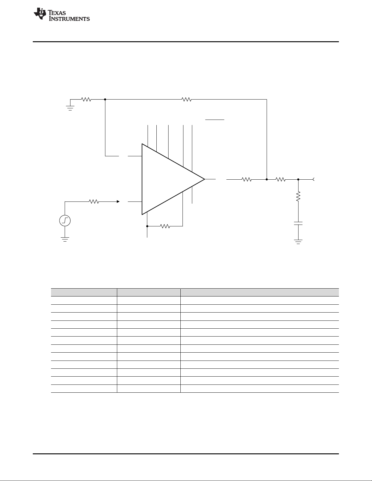
3 Configuration Examples
3.1 Noninverting Amplifier Configuration Setup
The EVM can be set to a noninverting amplifier configuration, as shown in Figure 1. This configuration can
be operated in dual-supply or single-supply mode.
Configuration Examples
Table 4 gives the noninverting amplifier configuration details.
Reference Setting Function
C15, C16, R17 Not installed —
R20, R21 0 Ω —
SBOU219–February 2020
Submit Documentation Feedback
Figure 1. Noninverting Amplifier Configuration Schematic
Table 4. Noninverting Configuration
J13 AVSS, GND Selects AVSS (dual supply) or GND (single supply)
J3 GND Routes Vin– across R9 to ground
J4 Vin+ Routes Vin+ across R10 to the input signal (J1)
J5-7, J9 Open —
C6, C7 Not installed —
R10 1 kΩ —
R16 10 kΩ —
J11 Open Output is enabled
J8 0.45 A Current limit set to 0.45 A
R26 Not installed —
Copyright © 2020, Texas Instruments Incorporated
OPA564DWP-EVM
7
Page 8
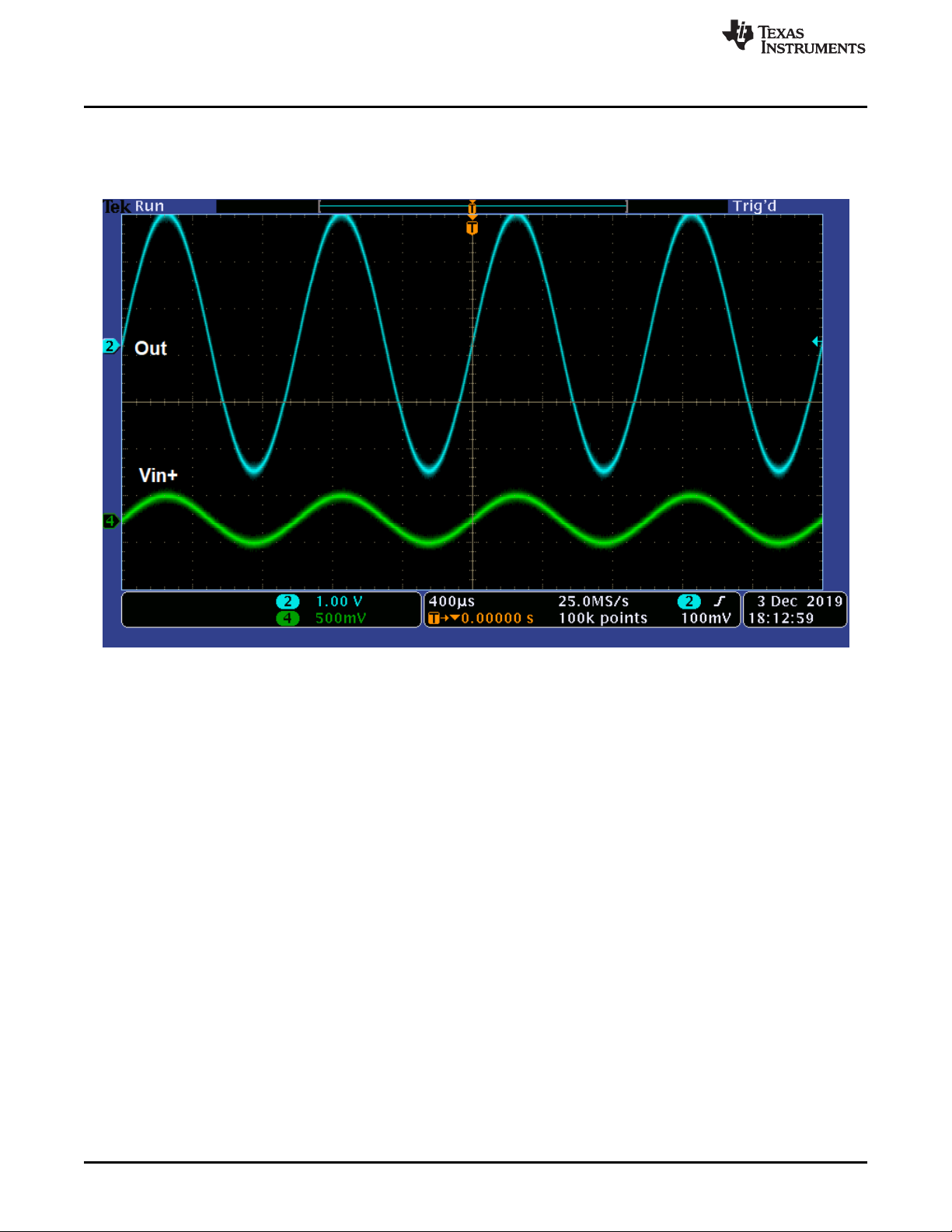
Configuration Examples
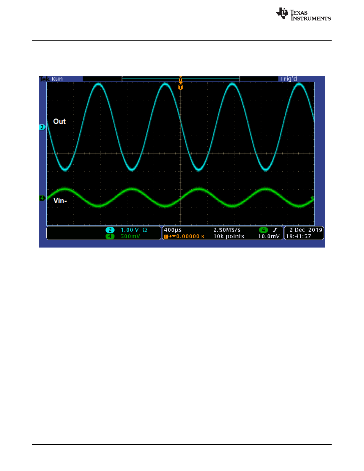
Figure 2 shows the expected results for the noninverting operation of the OPA564 with a gain of 11. A
dual supply is used, and the positive input signal is a sine wave with a peak-to-peak amplitude of 500 mV
and a frequency of 1 kHz. As expected, the output is a sine wave with 5.5-V peak-to-peak amplitude, in
phase with the input signal.
www.ti.com
Figure 2. Noninverting Operation
8
OPA564DWP-EVM
Copyright © 2020, Texas Instruments Incorporated
SBOU219–February 2020
Submit Documentation Feedback
Page 9

Current
Limit
Flag
Thermal
Flag
V
DIG
V+
Enable/Shutdown
T
SENSE
Current
Limit
Set
OPA564AIDWP
R
SET
(2)
(19)
(17, 18)
±IN
+IN
(6)
(7)
(3)
(8)
(4)
(15, 16)
R20 0
R16 10 k
R
9 1
k
R10 1 k
(9)
(12)
V±
(1, 10, 11, 20)
(13, 14)
V
OUT
R21 0
R24 10
C21 10 n
+
±
(5)
VOUT
Vin+
+
www.ti.com
3.2 Inverting Amplifier Configuration Setup
The inverting operation configuration of the EVM is shown in Figure 3. This configuration can be operated
in dual-supply or single-supply mode.
Configuration Examples
Table 5 describes the inverting amplifier PCB configuration.
C15, C16, R17 Not installed —
SBOU219–February 2020
Submit Documentation Feedback
Figure 3. Inverting Amplifier Configuration Schematic
Table 5. Inverting Configuration
Reference Setting Function
J13 AVSS, GND Selects AVSS (dual supply) or GND (single supply)
J3 Vin– Routes Vin– across R9 to input signal through J2
J5 GND Routes Vin+ across R10 to ground
J4, J6-7, J9 Open —
C6, C7 Not installed —
R9 1 kΩ —
R16 10 kΩ —
J11 Open Output is enabled
J8 0.45 A Current limit set to 0.45 A
R20, R21 0 Ω —
R26 Not installed —
Copyright © 2020, Texas Instruments Incorporated
OPA564DWP-EVM
9
Page 10
Configuration Examples
Figure 4 shows the expected results for the inverting operation of the OPA564 with a gain of –10. A dual
supply is used, and the negative input signal is a sine wave with a peak-to-peak amplitude of 500 mV and
a frequency of 1 kHz. As expected, the output is a sine wave with 5-V peak-to-peak amplitude, 180° out of
phase with the input signal.
www.ti.com
Figure 4. Inverting Operation
10
OPA564DWP-EVM
Copyright © 2020, Texas Instruments Incorporated
SBOU219–February 2020
Submit Documentation Feedback
Page 11

Current
Limit
Flag
Thermal
Flag
V
DIG
V+
Enable/Shutdown
T
SENSE
Current
Limit
Set
OPA564AIDWP
R
SET
(2)
(19)
(17, 18)
±IN
+IN
(6)
(7)
(3)
(8)
(4)
(15, 16)
R20 0
R16 10 k
R
9 1
k
R10 1 k
(9)
(12)
V±
(1, 10, 11, 20)
(13, 14)
V
OUT
R21 0
R24 10
C21 10n
+
±
(5)
VOUT
Vin+
+
R14 10 k
Vin±
+
www.ti.com
3.3 Differential Amplifier Configuration Setup
The EVM can also be set to a difference amplifier configuration, as shown in Figure 5. Both inputs are
driven in this mode, and the output is the difference between these inputs gained up by a factor of 10.
This configuration can be operated in dual-supply or single-supply mode.
Configuration Examples
Table 6 describes the differential amplifier PCB configuration.
Reference Setting Function
C15, C16, R17 Not installed —
R20, R21 0 Ω —
SBOU219–February 2020
Submit Documentation Feedback
Figure 5. Differential Amplifier Configuration Schematic
Table 6. Differential Configuration
J13 AVSS, GND Selects AVSS (dual supply) or GND (single supply)
J3 Vin– Routes Vin– across R9 to input signal via J2
J4 Vin+ Routes Vin+ across R10 to the input signal (J1)
J5-7 Open —
J9 GND References Vin+ to GND through R14
Copyright © 2020, Texas Instruments Incorporated
R14 10 kΩ —
C6, C7 Not installed —
R9, R10 1 kΩ —
R16 10 kΩ —
J11 Open Output is enabled
J8 0.45 A Current limit set to 0.45 A
R26 Not installed —
OPA564DWP-EVM
11
Page 12
Configuration Examples
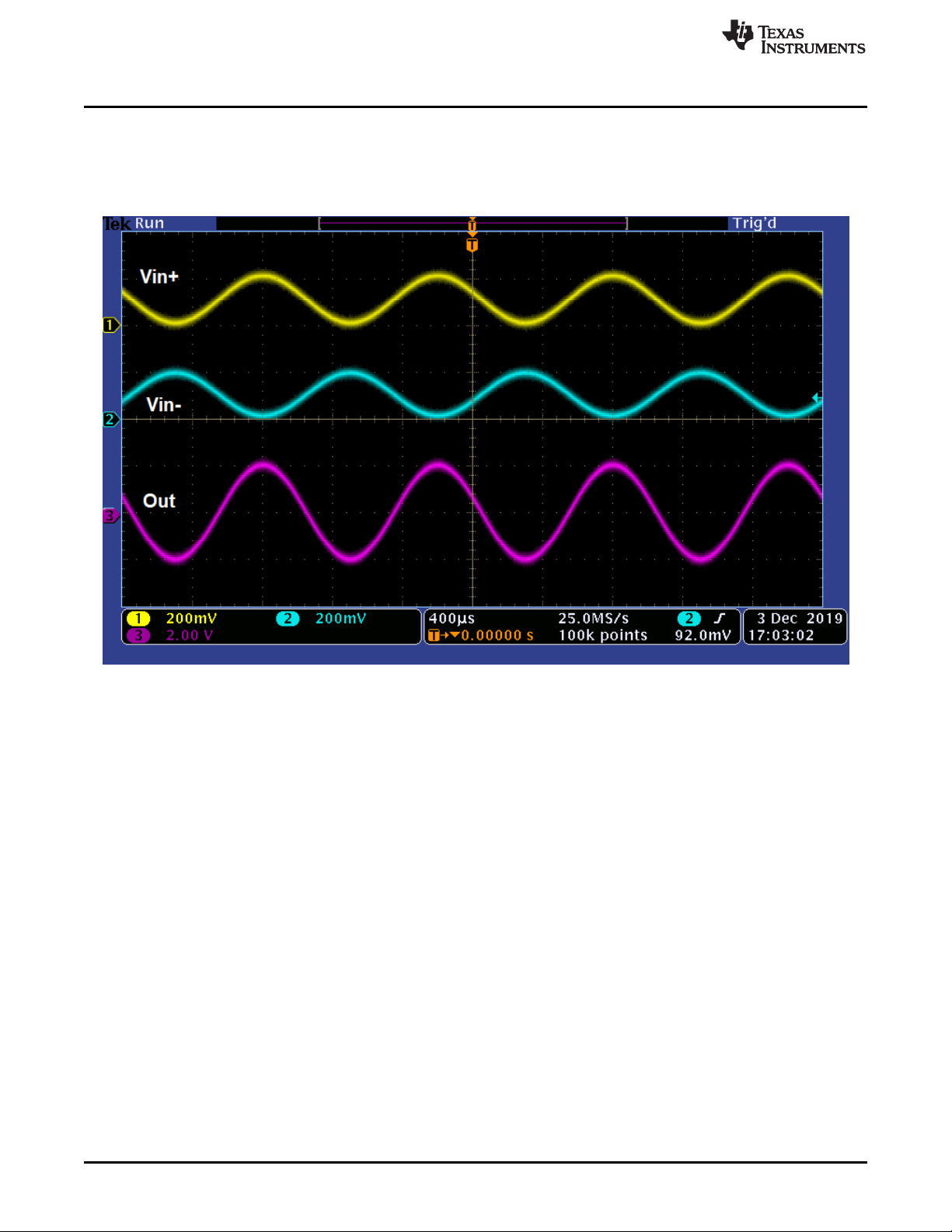
Figure 6 shows the expected results for the differential operation of the OPA564 with a gain of 10. Dual
supply is used. The input signals are sinusoids with a peak-to-peak amplitude of 200 mV and a frequency
of 1 kHz. The negative input signal has a phase shift of 180° relative to the positive input signal. As
expected, the difference of the input signals is amplified by a factor of 10, resulting in a sinusoid of 4-V
peak-to-peak amplitude in phase with Vin+, on the output.
www.ti.com
Figure 6. Differential Operation
12
OPA564DWP-EVM
Copyright © 2020, Texas Instruments Incorporated
SBOU219–February 2020
Submit Documentation Feedback
Page 13
Current
Limit
Flag
Thermal
Flag
V
DIG
V+
Enable/Shutdown
T
SENSE
Current
Limit
Set
OPA564AIDWP
R
SET
(2)
(19)
(17, 18)
±IN
+IN
(6)
(7)
(3)
(8)
(4)
(15, 16)
R20 0
R16 1 k
R
9 10
k
R10 10 k
(9)
(12)
V±
(1, 10, 11, 20)
(13, 14)
V
OUT
R21 1
R24 10
C21 10 n
+
±
(5)
R17 1 k
R Ext
10
A
+
A-Meter
VOUT
Vin+
+
www.ti.com
3.4 Improved Howland Current Pump Configuration Setup
The OPA564DWP-EVM can also be configured as an improved Howland current pump, delivering precise
current to a load. The output current can be adjusted from very low (in microamp range) to the maximum
output current of the device (1.5 A), as long as the amplifier does not exceed the absolute maximum
ratings (such as output voltage swing, slew rate, and so on.). Detailed information on the basic and
improved Howland current pump can be found in the AN1515 A Comprehensive Study of the Howland
Current Pump application note.
The improved Howland current pump is applied by configuring the EVM according to the schematic shown
in Figure 7. This default configuration delivers approximately 100 mA of current for every 1 V of input.
Configuration Examples
Table 7 shows the improved Howland current pump PCB configuration.
Reference Setting Function
SBOU219–February 2020
Submit Documentation Feedback
Figure 7. Improved Howland Current Pump Schematic
Table 7. Improved Howland Current Pump Configuration
J13 AVSS Selects AVSS (dual supply)
J3 GND Routes Vin– across R9 to ground
J4 Vin+ Routes Vin+ across R10 to the input signal (J1)
J5-7, J9 Open —
C6, C7 Not installed —
R9, R10 10 kΩ —
R16, R17 1 kΩ —
C15, C16 Not installed —
J11 Open Output is enabled
J8
R20 0 Ω —
R21 1 Ω —
R26 Not installed —
R Ext 10 Ω —
0.45 A, 0.65 A, 1.41 A or
custom value
Copyright © 2020, Texas Instruments Incorporated
Sets the current limit to 0.45 A, 0.65 A, 1.41 A, or a custom current
limit value through R5
OPA564DWP-EVM
13
Page 14

out
1.000 V 0 V 1.000 k
1.000 10.00 k
:
§ ·
¨ ¸
: :
© ¹
R9 R10
R16 R17 R21
out
(Vin+) (Vin ) R16
R21 R9
u
Configuration Examples
Some of the OPA564DWP-EVM resistors are different than in the three previous amplifier configurations
to accommodate the improved Howland current pump circuit. The mathematical relationship between the
resistors outlined in the AN-1515 application report must be observed to maintain correct output current
from the pump.
The output current is established by Equation 2:
The mathematical relationship to be observed is shown in Equation 3:
According to Equation 3, if R9 = R10, then R16 = R17 + R21.
For a default setup:
• Let R9 = R10 = 10.00 kΩ, R16 = 1.000 kΩ, and R21 = 1.000 Ω.
• Then, R17 = R16 – R21 = 1.000 kΩ – 1.000 Ω = 999 Ω ≅ 1.000 kΩ
• R17 is not populated with the 1.000-kΩ resistor.
• R21, a 0-Ω resistor, is replaced and populated with the 1.000-Ω resistor.
• Apply Equation 2 to solve for I
The improved Howland current pump configured with these resistor values sources an output current of
0.1 A when 1.000 V is applied to the OPA564 Vin+ input. If Vin+ is increased to 2.000 V, the output
current doubles to 0.2 A. If dual polarity supplies, such as ±12 V, are being used with the OPA564DWPEVM, and the polarity of Vin+ is reversed or the positive voltage is applied to Vin–, the output current
reverses direction. In this case, the OPA564 sinks 0.1 A. Keep in mind that with any current source that
includes the improved Howland current source, an output load must be provided for the load current to
flow through. A specific range of load resistances from a minimum of 0 Ω to a maximum value set by
Ohm's law. The maximum is limited by the OPA564 maximum output voltage swing (V
output current (I
in Equation 4:
out
), or mathematically stated: R
out
LOAD(MAX)
= V
out(MAX)
/ I
out
www.ti.com
(2)
(3)
(4)
) and the pump
out
.
14
OPA564DWP-EVM
Copyright © 2020, Texas Instruments Incorporated
SBOU219–February 2020
Submit Documentation Feedback
Page 15

Current
Limit
Flag
Thermal
Flag
V
DIG
V+
Enable/Shutdown
T
SENSE
Current
Limit
Set
OPA564AIDWP
R
SET
(2)
(19)
(17, 18)
±IN
+IN
(6)
(7)
(3)
(8)
(4)
(15, 16)
R20 0
R16 10 kR9 1 k
R10 k
(9)
(12)
V±
(1, 10, 11, 20)
(13, 14)
V
OUT
Current
Limit
Flag
Thermal
Flag
V
DIG
V+
Enable/Shutdown
T
SENSE
Current
Limit
Set
OPA564AIDWP
R
SET
(2)
(19)
(17, 18)
±IN
+IN
(6)
(7)
(3)
(8)
(4)
(15, 16)
R20 0
R16 1 kR9 1 k
R10 1 k
(9)
(12)
(1, 10, 11, 20)
(13, 14)
V
OUT
R21 0
R Ext 35
R24
10
C21
10 n
R21 0
VOUT1
VOUT2
+
±
(5)
(5)
Vin+
+
R24 10
C21 10 n
www.ti.com
3.5 Bridge-Tied Load Configuration Setup
Another configuration that can be used with the OPA564DWP-EVM is the bridge-tied load (BTL).
However, this configuration requires two EVMs. The first EVM must be set up in a noninverting amplifier
configuration, and the second in an inverting amplifier configuration, Figure 8. This configuration can be
operated in dual-supply or single-supply mode.
Configuration Examples
Table 8 and Table 9 describe the bridge-tied load configuration for the first and second PCB, respectively.
Board 1: Noninverting Amplifier
SBOU219–February 2020
Submit Documentation Feedback
C15, C16, R17 Not installed —
Figure 8. Bridge-Tied Load Schematic
Table 8. Bridge-Tied Load Configuration: Board 1
Reference Setting Function
J13 AVSS, GND
J3 GND Routes Vin– across R9 to ground
J4 Vin+
J5-7, J9 Open —
C6, C7 Not installed —
R9, R10 1 kΩ —
R16 10 kΩ —
J11 Open Output is enabled
J8 0.45 A Current limit set to 0.45 A
R20, R21 0 Ω —
R26 Not installed —
Copyright © 2020, Texas Instruments Incorporated
Selects AVSS (dual supply) or GND
(single supply)
Routes Vin+ across R10 to the input
signal (J1)
OPA564DWP-EVM
15
Page 16

Configuration Examples
Board 2: Inverting Amplifier
Reference Setting Function
J13 AVSS, GND
J3 Vin–
J5 GND Routes Vin+ across R10 to ground
J4, J6-7, J9 Open —
C6, C7 Not installed —
R9 1 kΩ —
R16 1 kΩ —
C15, C16, R17 Not installed —
J11 Open Output is enabled
J8 0.45 A Current limit set to 0.45 A
R20, R21 0 Ω —
R26 Not installed —
As mentioned earlier, the BTL circuit consists of one noninverting and one inverting amplifier stage. By
default, the noninverting stage is set up with a gain of 11; whereas, the inverting stage is set with a gain of
–1.Given that the inverting input comes from the output of the noninverting stage, the total gain of the
inverting stage is therefore –11. Combining the outputs of the two stages gives double the amplification, a
total gain of 22.
Figure 9 shows the expected results for the bridge-tied load operation of the OPA564, used in dual-supply
mode. Input signal Vin+ of the first board is a sinusoid with a peak-to-peak amplitude of 100 mV and a
frequency of 1 kHz. The final output signal is taken across an external 35-Ω connecting output of the first
board with the output of the second board. As expected, a difference of one sinusoid with a gain of 11 and
another with the gain of –11, gives an input signal amplification factor of 22. A 100-mV peak-to-peak
amplitude input signal is amplified to a sinusoid of 2.2-V peak-to-peak amplitude, 180° out of phase with
the input signal.
www.ti.com
Table 9. Bridge-Tied Load Configuration: Board 2
Selects AVSS (dual supply) or GND (single
supply)
Routes Vin– across R9 to input signal
through J2
16
OPA564DWP-EVM
Figure 9. Bridge-Tied Load Operation
Copyright © 2020, Texas Instruments Incorporated
SBOU219–February 2020
Submit Documentation Feedback
Page 17

V-
1
V+
2
TFLAG
3
E/S
4
IN+
5
IN-
6
VDIG
7
IFLAG
8
ISET
9
V-
10
V-
11
TSENSE
12
V-PWR
13
V-PWR
14
VOUT
15
VOUT
16
V+ PWR
17
V+ PWR
18
V+ PWR
19
V-
20
EP
21
OPA564AIDWP
U4
J14
GND
J10
AVDD
V-
12.0k
R13
31.6k
R12
47.5k
R11
680pF
C4
Iset
1
2
D1
V+
V-
2.20k
R1
TP6
AVDD
GND
0
R15
AVDD
V-
J12
AVSS
TP8
V-
1
2
3
J13
GND
AVSS
TP9
GND
TP10
GND
GND
IN1OUT
2
OUT
3
4
NC5OUT
6
OUT
7
NC
8
ADJ
U2
V-
0.1uF
C2
AVDD
V-
TP4
Vdig
Vdig
V-
499
R7
1.50k
R8
6800pF
C3
Vdig
0.1uF
C11
GND
V+
0.1uF
C12
GND
E/S
TflagIflag
Iset
Tsense
GND
V-
0.1uF
C13
GND
V+
D5
1
2
345
J1
Vin+
1
2
345
J2 Vin-
GND
1
2
3
J3
-IN Select
GND
TP2
-IN
GND
1
2
J4
Vin+
1
2
J5
GND
1
2
J6
Userselect Vref
1
2
J7
Vref
V+
V-
DNI
R3
DNI
R4
1.00k
R10
TP3
+IN
GND
DNI
C7
GND
DNI
C6
GND
1.00k
R9
DNI
C15
DNI
C16
10.0k
R16
TP5
Vref
D6
DNI
GND
1
3
2
D3
V-
AVDD
J16
GND
GND
DNI
R26
0.01uF
C21
10.0
R24
GND
J15
OUT
0
R200R21
R17
DNI
0.1uF
C17
D8
DNI
GND
D7
V- V-
GND
1
2 5
43
6
U5
4N38SR2M
Vdig
0.1uF
C18
3.92k
R19
100k
R22
22.0k
R23
21.0k
R25
351
2
4
678
9
Q1
100k
R29
0.1uF
C24
D10
V+
TP13
V+
V-
1.00M
R27
1000pF
C23
1
2
D2
IFlag
42
U1A
VCC5GND
3
NC
1
U1B
Vdig
1.00k
R2
V-
0.1uF
C1
Vdig V-
Iflag
TP1
IFlag
1
2
D9
TFlag
42
U6A
VCC5GND
3
NC
1
U6B
1.00k
R28
Vdig
Tflag
V-
V-
0.1uF
C22
Vdig
TP11
TFlag
Tsense
TP14
TSense
42
U3A
VCC5GND
3
NC
1
SN74LVC1G04DBVR
U3B
V-
0.1uF
C9
Vdig
1
2
D4
1.00k
R18
1
2
J11
Disable
E/S
TP7
E/S
V-
GND
1uF
C5
GND
V-
0.1uF
C19
0.1uF
C20
GND
47pF
C10
47pF
C14
1
234
5
J17
Vout
GND
TP12
Vout
TP15
GND
DNI
R5
1
2345678
J8
Iset
DNI
R6
GND
10.0k
R14
1
2
J9 Vin+
GND
www.ti.com
4 Schematics, PCB Layout, and Bill of Materials
4.1 Schematics
The schematic of the EVM, including the enable and shutdown and LED circuits, is shown in Figure 10.
Schematics, PCB Layout, and Bill of Materials
SBOU219–February 2020
Submit Documentation Feedback
Figure 10. OPA564DWP-EVM Schematic
Copyright © 2020, Texas Instruments Incorporated
OPA564DWP-EVM
17
Page 18

Schematics, PCB Layout, and Bill of Materials
4.2 PCB Layout
The EVM top and bottom layers are illustrated in Figure 11 and Figure 12, respectively.
Three banana jacks supply power to the EVM (see Section 2.2) . J13 is used to set operation to single
supply or dual supply.
Voltage inputs, Vin+ and Vin–, are on the left-hand side of the board. Jumpers J3 to J6 are used for
setting the input voltage value. Test point TP5 is used to supply reference voltage to the board. Jumper J7
can then be used to offset Vin+ by reference voltage value. Jumper J9 is used for referencing the
noninverting input to ground using a 10-kΩ resistor. This setup is used for difference amplifier operation.
R16, R17, C15, C16 are user-selectable op amp feedback components. R20 and R21 are the output
current-limiting resistors. R20 and R21 are set to 0 Ω by default, but can be adjusted to act as isolation
resistors for improved stability or to set the output current when the device is configured as an improved
Howland current pump (see Section 3.4). However, setting R20 or R21 to value greater than 0 Ω creates a
low-pass filter with the output compensation consisting of R24 and C21.
Vout (pins 15 and 16 of OPA564) can be accessed through connector J17, as well as through banana
jack J15 (see Section 2.3). Jack J16 is set to GND; thus, reading the output signal from J15 and J16 with
an oscilloscope is very convenient. Two super fast diodes (D6 and D8) are used for output protection.
Additionally, the board contains two empty footprints (D5 and D6) that can be used to add power-supply
protection diodes or transient voltage suppressor (TVS) diodes.
www.ti.com
18
OPA564DWP-EVM
Copyright © 2020, Texas Instruments Incorporated
SBOU219–February 2020
Submit Documentation Feedback
Page 19

www.ti.com
Schematics, PCB Layout, and Bill of Materials
SBOU219–February 2020
Submit Documentation Feedback
Figure 11. OPA564DWP-EVM, Top Layer
Copyright © 2020, Texas Instruments Incorporated
OPA564DWP-EVM
19
Page 20

Schematics, PCB Layout, and Bill of Materials
www.ti.com
20
OPA564DWP-EVM
Figure 12. OPA564DWP-EVM Bottom Layer
Copyright © 2020, Texas Instruments Incorporated
SBOU219–February 2020
Submit Documentation Feedback
Page 21

www.ti.com
4.3 Bill of Materials
Table 10 lists the bill of materials (BOM).
Designator Quantity Description PartNumber Manufacturer
C1, C2, C9, C11, C12,
C13, C17, C18, C19,
C20, C22, C24
C3 1 CAP, CERM, 6800 pF, 50 V, +/- 10%,
C4 1 CAP, CERM, 680 pF, 50 V, +/- 10%,
C5 1 CAP, CERM, 1 uF, 50 V, +/- 10%, X7R,
C10, C14 2 CAP, CERM, 47 pF, 50 V, +/- 5%,
C21 1 CAP, CERM, 0.01 uF, 50 V, +/- 10%,
C23 1 CAP, CERM, 1000 pF, 1000 V, +/- 10%,
D1 1 LED, Green, SMD LTST-C190GKT Lite-On
D2 1 LED, Orange, SMD LTST-C190KFKT Lite-On
D3 1 Diode, Schottky, 40 V, 0.2 A, SOT-23 BAS40-04-7-F Diodes Inc.
D4 1 LED, Yellow, SMD LY L29K-H1K2-26-Z OSRAM
D5, D7 2 Diode, Ultrafast, 50 V, 1 A, SMA ES1A-13-F Diodes Inc.
D9 1 LED, Red, SMD LS L29K-G1J2-1-Z OSRAM
D10 1 Diode, TVS, Uni, 12 V, SMA SMAJ12A Littelfuse
H1, H3, H5, H8 4 2203 Keystone
H2, H4, H6, H7 4 MACHINE SCREW PAN PHILLIPS 4-40 PMSSS 440 0025 PH B&F Fastener
J1, J2, J17 3 Connector, TH, BNC Right angle, 50
J3, J13 2 Header, 100mil, 3x1, Gold, SMT TSM-103-01-L-SV Samtec
J4, J5, J6, J7, J9, J11 6 Header, 100mil, 2x1, Gold with Tin Tail,
J8 1 Header, 2.54mm, 4x2, Gold, SMT TSM-104-01-L-DV Samtec
J10, J12, J14, J15, J16 5 Standard Banana Jack, Uninsulated,
Q1 1 MOSFET, P-CH, -20 V, -15 A,
R1 1 RES, 2.20 k, 1%, 0.25 W, 1206 RC1206FR-072K2L Yageo America
R2, R9, R10, R18, R28 5 RES, 1.00 k, 1%, 0.25 W, 1206 RC1206FR-071KL Yageo America
R7 1 RES, 499, 1%, 0.25 W, 1206 RC1206FR-07499RL Yageo America
R8 1 RES, 1.50 k, 1%, 0.25 W, 1206 RC1206FR-071K5L Yageo America
R11 1 RES, 47.5 k, 1%, 0.25 W, 1206 RC1206FR-0747K5L Yageo America
R12 1 RES, 31.6 k, 1%, 0.25 W, 1206 RC1206FR-0731K6L Yageo America
R13 1 RES, 12.0 k, 1%, 0.25 W, 1206 RC1206FR-0712KL Yageo America
R14, R16 2 RES, 10.0 k, 1%, 0.25 W, 1206 RC1206FR-0710KL Yageo America
R15, R20, R21 3 RES, 0, 5%, 0.75 W, AEC-Q200 Grade
R19 1 RES, 3.92 k, 1%, 0.25 W, 1206 RC1206FR-073K92L Yageo America
R22, R29 2 RES, 100 k, 1%, 0.25 W, 1206 RC1206FR-07100KL Yageo America
R23 1 RES, 22.0 k, 1%, 0.25 W, 1206 RC1206FR-0722KL Yageo America
R24 1 RES, 10.0, 1%, 0.25 W, 1206 RC1206FR-0710RL Yageo America
Table 10. Bill of Materials
12 CAP, CERM, 0.1 uF, 50 V, +/- 10%,
X7R, 1206
X7R, 1206
X7R, 1206
1206
C0G/NP0, 0805
X7R, 1206
X7R, 1206
ohm gold
SMT
5.5mm
DNH0008A (VSONP-8)
0, 2010
Schematics, PCB Layout, and Bill of Materials
C1206C104K5RACTU Kemet
12065C682KAT2A AVX
CC1206KRX7R9BB681 Yageo America
C3216X7R1H105K160AB TDK
GQM2195C1H470JB01D MuRata
12065C103KAT2A AVX
CC1206KKX7RCBB102 Yageo America
Supply
5413631-2 AMP
TSM-102-02-L-SV Samtec
575-4 Keystone
CSD25402Q3A Texas Instruments
CRCW20100000Z0EF Vishay-Dale
SBOU219–February 2020
Submit Documentation Feedback
Copyright © 2020, Texas Instruments Incorporated
OPA564DWP-EVM
21
Page 22

Schematics, PCB Layout, and Bill of Materials
Designator Quantity Description PartNumber Manufacturer
R25 1 RES, 21.0 k, 1%, 0.25 W, 1206 RC1206FR-0721KL Yageo America
R27 1 RES, 1.00 M, 1%, 0.25 W, 1206 MCR18EZHF1004 Rohm
TP1, TP2, TP3, TP4,
TP5, TP6, TP7, TP8,
TP9, TP10, TP11,
TP12, TP13, TP14,
TP15
U1, U3, U6 3 Single Inverter, DBV0005A, LARGE
U2 1 Adjustable Regulator with 3.7 to 38 V
U4 1 1.5 A, 17 MHz, Power Operational
U5 1 Optocoupler, 4.17 kV, 20% min CTR,
C6, C7, C15, C16 0 CAP, CERM, 0.1 uF, 50 V, +/- 10%,
D6, D8 0 Diode, TVS, Uni, 12 V, SMA SMAJ12A Littelfuse
FID1, FID2, FID3 0 Fiducial mark. There is nothing to buy or
R3, R4, R17 0 RES, 10.0 k, 1%, 0.25 W, 1206 RC1206FR-0710KL Yageo America
R5 0 RES, 12.0 k, 1%, 0.25 W, 1206 RC1206FR-0712KL Yageo America
R6 0 RES, 1.00 k, 1%, 0.25 W, 1206 RC1206FR-071KL Yageo America
R26 0 RES, 0, 5%, 0.75 W, AEC-Q200 Grade
15 Test Point, Compact, SMT 5016 Keystone
T&R
Input and 1.2 to 32 V Output, 0 to 125
degC, 8-Pin SOIC (D), Green (RoHS &
no Sb/Br)
Amplifier, 7 to 24 V, -40 to 125 degC,
20-pin SOP (DWP20), Green (RoHS &
no Sb/Br)
SMT
X7R, 1206
mount.
0, 2010
www.ti.com
Table 10. Bill of Materials (continued)
SN74LVC1G04DBVR Texas Instruments
LM317LCD Texas Instruments
OPA564AIDWP Texas Instruments
4N38SR2M Fairchild
Semiconductor
C1206C104K5RACTU Kemet
N/A N/A
CRCW20100000Z0EF Vishay-Dale
22
OPA564DWP-EVM
Copyright © 2020, Texas Instruments Incorporated
SBOU219–February 2020
Submit Documentation Feedback
Page 23

IMPORTANT NOTICE AND DISCLAIMER
TI PROVIDES TECHNICAL AND RELIABILITY DATA (INCLUDING DATASHEETS), DESIGN RESOURCES (INCLUDING REFERENCE
DESIGNS), APPLICATION OR OTHER DESIGN ADVICE, WEB TOOLS, SAFETY INFORMATION, AND OTHER RESOURCES “AS IS”
AND WITH ALL FAULTS, AND DISCLAIMS ALL WARRANTIES, EXPRESS AND IMPLIED, INCLUDING WITHOUT LIMITATION ANY
IMPLIED WARRANTIES OF MERCHANTABILITY, FITNESS FOR A PARTICULAR PURPOSE OR NON-INFRINGEMENT OF THIRD
PARTY INTELLECTUAL PROPERTY RIGHTS.
These resources are intended for skilled developers designing with TI products. You are solely responsible for (1) selecting the appropriate
TI products for your application, (2) designing, validating and testing your application, and (3) ensuring your application meets applicable
standards, and any other safety, security, or other requirements. These resources are subject to change without notice. TI grants you
permission to use these resources only for development of an application that uses the TI products described in the resource. Other
reproduction and display of these resources is prohibited. No license is granted to any other TI intellectual property right or to any third
party intellectual property right. TI disclaims responsibility for, and you will fully indemnify TI and its representatives against, any claims,
damages, costs, losses, and liabilities arising out of your use of these resources.
TI’s products are provided subject to TI’s Terms of Sale (www.ti.com/legal/termsofsale.html) or other applicable terms available either on
ti.com or provided in conjunction with such TI products. TI’s provision of these resources does not expand or otherwise alter TI’s applicable
warranties or warranty disclaimers for TI products.
Mailing Address: Texas Instruments, Post Office Box 655303, Dallas, Texas 75265
Copyright © 2020, Texas Instruments Incorporated
 Loading...