


LM124, LM124A, LM224, LM224A
LM324, LM324A, LM324Y, LM2902, LM2902Q
QUADRUPLE OPERATIONAL AMPLIFIERS
SLOS066E– SEPTEMBER 1975 – REVISED FEBRUARY1997
3–1
POST OFFICE BOX 655303 • DALLAS, TEXAS 75265
D
Wide Range of Supply Voltages:
Single Supply...3 V to 30 V
(LM2902 and LM2902Q
3 V to 26 V), or Dual Supplies
D
Low Supply Current Drain Independent of
Supply Voltage . . . 0.8 mA Typ
D
Common-Mode Input Voltage Range
Includes Ground Allowing Direct Sensing
Near Ground
D
Low Input Bias and Offset Parameters:
Input Offset Voltage ...3 mV Typ
A Versions ...2 mV Typ
Input Offset Current...2 nA Typ
Input Bias Current...20 nA Typ
A Versions . . . 15 nA Typ
D
Differential Input Voltage Range Equal to
Maximum-Rated Supply Voltage . . . 32 V
(26 V for LM2902 and LM2902Q)
D
Open-Loop Differential Voltage
Amplification . . . 100 V/mV Typ
D
Internal Frequency Compensation
description
These devices consist of four independent
high-gain frequency-compensated operational
amplifiers that are designed specifically to operate
from a single supply over a wide range of voltages.
Operation from split supplies is also possible
when the difference between the two supplies is
3 V to 30 V (for the LM2902 and LM2902Q, 3 V to
26 V) and V
CC
is at least 1.5 V more positive than
the input common-mode voltage. The low supply
current drain is independent of the magnitude of
the supply voltage.
Applications include transducer amplifiers, dc amplification blocks, and all the conventional operational
amplifier circuits that now can be more easily implemented in single-supply-voltage systems. For example, the
LM124 can be operated directly from the standard 5-V supply that is used in digital systems and easily provides
the required interface electronics without requiring additional ±15-V supplies.
The LM2902Q is manufactured to demanding automotive requirements.
The LM124 and LM124A are characterized for operation over the full military temperature range of –55°C to
125°C. The LM224 and LM224A are characterized for operation from –25°C to 85°C. The LM324 and LM324A
are characterized for operation from 0°C to 70°C. The LM2902 and LM2902Q are characterized for operation
from –40°C to 125°C.
Copyright 1997, Texas Instruments Incorporated
PRODUCTION DATA information is current as of publication date.
Products conform to specifications per the terms of Texas Instruments
standard warranty. Production processing does not necessarily include
testing of all parameters.
+
–
IN –
IN +
OUT
1
2
3
4
5
6
7
14
13
12
11
10
9
8
1OUT
1IN–
1IN+
V
CC
2IN+
2IN–
2OUT
4OUT
4IN–
4IN+
GND
3IN+
3IN–
3OUT
LM124, LM124A ...J OR W PACKAGE
ALL OTHERS . . . D, DB, N OR PW PACKAGE
(TOP VIEW)
3212019
910111213
4
5
6
7
8
18
17
16
15
14
4IN+
NC
GND
NC
3IN+
1IN+
NC
V
CC
NC
2IN+
LM124, LM124A . . . FK PACKAGE
(TOP VIEW)
1IN –
1OUT
NC
3IN –
4IN –
2IN –
2OUT
NC
NC – No internal connection
3OUT
4OUT
symbol (each amplifier)

LM124, LM124A, LM224, LM224A
LM324, LM324A, LM324Y, LM2902, LM2902Q
QUADRUPLE OPERATIONAL AMPLIFIERS
SLOS066E– SEPTEMBER 1975 – REVISED FEBRUARY1997
3–2
POST OFFICE BOX 655303 • DALLAS, TEXAS 75265
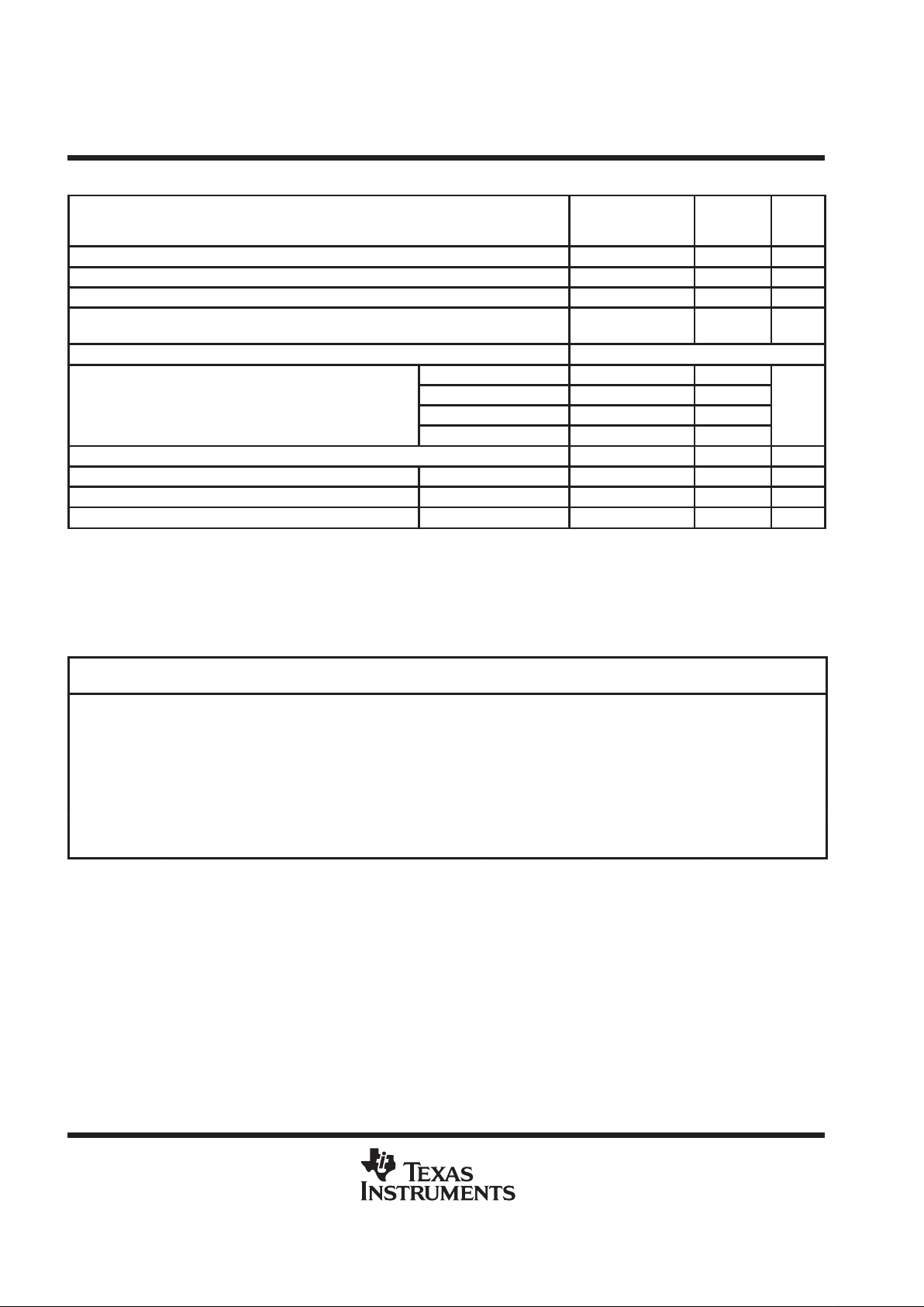
AVAILABLE OPTIONS
PACKAGED DEVICES
T
A
VIOmax
AT 25°C
SMALL
OUTLINE
(D)
†
VERY
SMALL
OUTLINE
(DB)
‡
CHIP
CARRIER
(FK)
CERAMIC
DIP
(J)
PLASTIC
DIP
(N)
TSSOP
(PW)
‡
FLAT
PACK
(W)
CHIP
FORM
(Y)
0°C to
7 mV LM324D LM324DBLE — — LM324N LM324PWLE —
70°C
3 mV LM324AD — — — LM324AN LM324APWLE —
LM324Y
–25°C to
5 mV LM224D — — — LM224N — —
85°C
3 mV LM224AD — — — LM224AN — —
—
–40°C to
LM2902D
— — LM2902N
—
125°C
7 mV
LM2902QD
LM2902DBLE
— — LM2902QN
LM2902PWLE
—
—
–55°C to 5 mV
— — LM124FK LM124J — —
LM124W
125°C 2 mV
— — LM124AFK LM124AJ — —
—
†
The D package is available taped and reeled. Add the suffix R to the device type (e.g., LM324DR).
‡
The DB and PW packages are only available left-end taped and reeled.
schematic (each amplifier)
To Other
Amplifiers
≈ 6-µA
Current
Regulator
V
CC
OUT
GND
IN –
IN +
≈ 100-µA
Current
Regulator
≈ 50-µA
Current
Regulator
COMPONENT COUNT
(total device)
Epi-FET
Transistors
Diodes
Resistors
Capacitors
1
95
4
11
4
≈ 6-µA
Current
Regulator

LM124, LM124A, LM224, LM224A
LM324, LM324A, LM324Y, LM2902, LM2902Q
QUADRUPLE OPERATIONAL AMPLIFIERS
SLOS066E– SEPTEMBER 1975 – REVISED FEBRUARY1997
3–3
POST OFFICE BOX 655303 • DALLAS, TEXAS 75265
LM324Y chip information
This chip, when properly assembled, displays characteristics similar to the LM324. Thermal compression or
ultrasonic bonding may be used on the doped-aluminum bonding pads. Chips may be mounted with conductive
epoxy or a gold-silicon preform.
BONDING PAD ASSIGNMENTS
1IN+
1IN–
2OUT
1OUT
2IN+
2IN–
V
CC+
3IN+
3IN–
4OUT
3OUT
4IN+
4IN–
GND
CHIP THICKNESS: 15 TYPICAL
BONDING PADS: 4 × 4 MINIMUM
TJmax = 150°C
TOLERANCES ARE ± 10%.
ALL DIMENSIONS ARE IN MILS.
PIN (11) IS INTERNALLY CONNECTED
TO BACKSIDE OF CHIP.
(3)
(2)
(7)
(10)
(9)
(14)
(1)
(5)
(6)
(8)
(12)
(13)
62
65
(1)
(2)
(3)
(4)
(5)
(6)
(7) (8)
(9)
(10)
(11)
(12)
(13)
(14)
(11)
(4)
LM124, LM124A, LM224, LM224A
LM324, LM324A, LM324Y, LM2902, LM2902Q
QUADRUPLE OPERATIONAL AMPLIFIERS
SLOS066E– SEPTEMBER 1975 – REVISED FEBRUARY1997
3–4
POST OFFICE BOX 655303 • DALLAS, TEXAS 75265
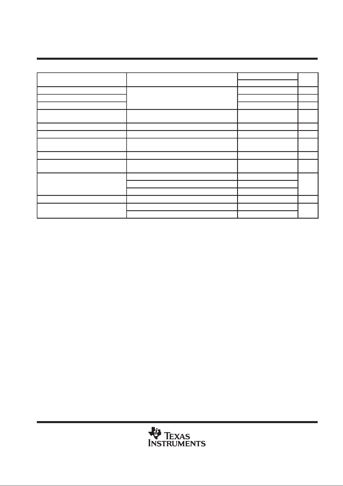
absolute maximum ratings over operating free-air temperature range (unless otherwise noted)
†
LM124, LM124A
LM224, LM224A
LM324, LM324A
LM2902,
LM2902Q
UNIT
Supply voltage, VCC (see Note 1) 32 26 V
Differential input voltage, VID (see Note 2) ±32 ±26 V
Input voltage, VI (either input) –0.3 to 32 –0.3 to 26 V
Duration of output short circuit (one amplifier) to ground at (or below) TA = 25°C,
VCC ≤ 15 V (see Note 3)
unlimited unlimited
Continuous total dissipation See Dissipation Rating Table
LM124, LM124A –55 to 125
p
p
LM224, LM224A –25 to 85
°
Operating free-air temperature range, T
A
LM324, LM324A 0 to 70
°C
LM2902, LM2902Q –40 to 125
Storage temperature range –65 to 150 –65 to 150 °C
Case temperature for 60 seconds FK package 260 °C
Lead temperature 1,6 mm (1/16 inch) from case for 60 seconds J or W package 300 300 °C
Lead temperature 1,6 mm (1/16 inch) from case for 10 seconds D, DB, N, or PW package 260 260 °C
†
Stresses beyond those listed under “absolute maximum ratings” may cause permanent damage to the device. These are stress ratings only, and
functional operation of the device at these or any other conditions beyond those indicated under “recommended operating conditions” is not
implied. Exposure to absolute-maximum-rated conditions for extended periods may affect device reliability.
NOTES: 1. All voltage values (except differential voltages and VCC specified for the measurement of IOS) are with respect to the network GND.
2. Differential voltages are at IN + with respect to IN –.
3. Short circuits from outputs to VCC can cause excessive heating and eventual destruction.
DISSIPATION RATING TABLE
PACKAGE
TA ≤ 25°C
POWER RATING
DERATING
FACTOR
DERATE
ABOVE T
A
TA = 70°C
POWER RATING
TA = 85°C
POWER RATING
TA = 125°C
POWER RATING
D 900 mW 7.6 mW/°C 32°C 611 mW 497 mW N/A
DB 775 mW 6.2 mW/°C25°C 496 mW 403 mW N/A
FK 900 mW 11.0 mW/°C68°C 878 mW 713 mW 273 mW
J (LM124_) 900 mW 11.0 mW/°C68°C 878 mW 713 mW 273 mW
J (all others) 900 mW 8.2 mW/°C40°C 654 mW 531 mW N/A
N 900 mW 9.2 mW/°C52°C 734 mW 596 mW N/A
PW 700 mW 5.6 mW/°C25°C 448 mW 364 mW N/A
W 900 mW 8.0 mW/°C 37°C 636 mW 516 mW 196 mW

LM124, LM124A, LM224, LM224A
LM324, LM324A, LM324Y, LM2902, LM2902Q
QUADRUPLE OPERATIONAL AMPLIFIER
SLOS066E – SEPTEMBER 1975 – REVISED FEBRUARY 1997
POST OFFICE BOX 655303 DALLAS, TEXAS 75265
• 3–5
electrical characteristics at specified free-air temperature, V
CC
= 5 V (unless otherwise noted)
LM124, LM224 LM324 LM2902, LM2902Q
PARAMETER
TEST CONDITIONS
†
T
A
‡
MIN TYP§MAX MIN TYP§MAX MIN TYP§MAX
UNIT
V
= 5 V to MAX,
25°C 3 5 3 7 3 7
VIOI
nput offset voltage
CC
,
VIC = V
ICR
min, VO = 1.4 V
Full range 7 9 10
m
V
25°C 2 30 2 50 2 50
IIOI
nput offset curren
t
V
O
=
1.4 V
Full range 100 150 300
n
A
25°C –20 – 150 –20 –250 –20 –250
IIBI
nput bias curren
t
V
O
=
1.4 V
Full range –300 –500 – 500
n
A
0 to
0 to
0 to
Common-mode input
25°C
V
CC
–
1.5
V
CC
–
1.5
V
CC
–
1
.5
V
ICR
voltage range
V
CC
=
5 V to MAX
0 to
0 to
0 to
V
Full
range
V
CC
–
2
V
CC
–
2
VCC–2
RL = 2 kΩ 25°C
VCC–
1.5
VCC–
1.5
V
OH
High-level output voltage
RL = 10 kΩ 25°C
VCC–1
.5
V
VCC = MAX, RL = 2 kΩ Full range 26 26 22
VCC = MAX, RL ≥ 10 kΩ Full range 27 28 27 28 23 24
V
OL
Low-level output voltage RL ≤ 10 kΩ Full range 5 20 5 20 5 20 mV
Large-signal differential V
= 15 V, V
= 1 V to 11 V,
25°C 50 100 25 100 100
A
VD
gg
voltage amplification
CC
,
O
,
RL = ≥ 2 kΩ
Full range 25 15 15
V/mV
CMRR Common-mode rejection ratio VIC = V
ICR
min 25°C 70 80 65 80 50 80 dB
Supply-voltage rejection ratio
k
SVR
ygj
(∆VCC/∆VIO)
25°C651006510050100
dB
VO1/VO2Crosstalk attenuation f = 1 kHz to 20 kHz 25°C 120 120 120 dB
V
= 15 V,V
= 1 V
,
25°C –20 –30 –60 –20 –30 –60 –20 –30 –60
V
CC
15
V, V
ID
1
V,
VO = 0
Full range –10 –10 –10
I
O
Output current
V
= 15 V, V
= –1 V ,
25°C 10 20 10 20 10 20
mA
CC
,
ID
,
VO = 15 V
Full range 5 5 5
VID = –1 V , VO = 200 mV 25°C 12 30 12 30 30 µA
I
OS
Short-circuit output current
VCC at 5 V,
GND at –5 V
VO = 0
25°C ± 40 ± 60 ±40 ±60 ± 40 ±60 mA
VO = 2.5 V, No load Full range 0.7 1.2 0.7 1.2 0.7 1.2
I
CC
Supply current (four amplifiers)
VCC = MAX,
VO = 0.5 VCC, No load
Full range 1.4 3 1.4 3 1.4 3
mA
†
All characteristics are measured under open-loop conditions with zero common-mode input voltage unless otherwise specified. MAX VCC for testing purposes is 26 V for LM2902
and LM2902Q, 30 V for the others.
‡
Full range is –55°C to 125°C for LM124, –25°C to 85°C for LM224, 0°C to 70°C for LM324, and –40°C to 125°C for LM2902 and LM2902Q.
§
All typical values are at TA = 25°C.

LM124, LM124A, LM224, LM224A
LM324, LM324A, LM324Y, LM2902, LM2902Q
QUADRUPLE OPERATIONAL AMPLIFIERS
SLOS066E – SEPTEMBER 1975 – REVISED FEBRUARY 1997
Template Release Date: 7–11–94
3–6
POST OFFICE BOX 655303 DALLAS, TEXAS 75265
•
electrical characteristics at specified free-air temperature, VCC = 5 V (unless otherwise noted)
LM124A LM224A LM324A
PARAMETER
TEST CONDITIONS
†
T
A
‡
MIN
TYP
§
MAX MIN
TYP
§
MAX MIN
TYP
§
MAX
UNIT
V
= 5 V to 30 V,
25°C 2 2 3 2 3
VIOI
nput offset voltage
CC
,
VIC = V
ICR
min, VO = 1.4 V
Full range 4 4 5
m
V
25°C 10 2 15 2 30
IIOI
nput offset curren
t
V
O
=
1.4 V
Full range 30 30 75
n
A
25°C –50 –15 –80 –15 – 100
IIBI
nput bias curren
t
V
O
=
1.4 V
Full range –100 –100 –200
n
A
Common-mode input
25°C
0 to
VCC–1.5
0 to
VCC–1.5
0 to
VCC–1.5
V
ICR
voltage range
V
CC
=
30 V
Full range
0 to
VCC–2
0 to
VCC–2
0 to
VCC–2
V
RL = 2 kΩ 25°C VCC–1.5 VCC–1.5 VCC–1.5
V
OH
High-level output voltage
VCC = 30 V,
RL = 2 kΩ Full range 26 26 26
V
VCC = 30 V, RL ≥ 10 kΩ Full range 27 27 28 27 28
V
OL
Low-level output voltage RL ≤ 10 kΩ Full range 20 5 20 5 20 mV
A
VD
Large-signal differential
voltage amplification
VCC = 15 V, VO = 1 V to 11 V,
RL= ≥ 2 kΩ
Full range 25 25 15 V/mV
CMRR Common-mode rejection ratio VIC = V
ICR
min 25°C 70 70 80 65 80 dB
k
SVR
Supply-voltage rejection ratio
(∆VCC/∆VIO)
25°C 65 65 100 65 100 dB
VO1/VO2Crosstalk attenuation f = 1 kHz to 20 kHz 25°C 120 120 120 dB
V
= 15 V, V
= 1 V,
25°C –20 –20 –30 –60 –20 –30 –60
CC
,
ID
,
VO = 0
Full range –10 –10 –10
I
O
Output current
V
= 15 V, V
= –1 V ,
25°C 10 10 20 10 20
m
A
CC
,
ID
,
VO = 15 V
Full range 5 5 5
VID = –1 V , VO = 200 mV 25°C 12 12 30 12 30 µA
I
OS
Short-circuit output current
VCC at 5 V, GND at –5 V,
VO = 0
25°C ±40 ±60 ±40 ±60 ± 40 ±60 mA
VO = 2.5 V, No load Full range 0.7 1.2 0.7 1.2 0.7 1.2
I
CC
Supply current (four amplifiers)
VCC = 30 V, VO = 15 V,
No load
Full range 1.4 3 1.4 3 1.4 3
mA
†
All characteristics are measured under open-loop conditions with zero common-mode input voltage unless otherwise specified.
‡
Full range is –55°C to 125°C for LM124A, –25°C to 85°C for LM224A, and 0°C to 70°C for LM324A.
§
All typical values are at TA = 25°C.
LM124, LM124A, LM224, LM224A
LM324, LM324A, LM324Y, LM2902, LM2902Q
QUADRUPLE OPERATIONAL AMPLIFIERS
SLOS066E – SEPTEMBER 1975 – REVISED FEBRUARY 1997
7
POST OFFICE BOX 655303 • DALLAS, TEXAS 75265
electrical characteristics, VCC = 5 V, TA = 25°C (unless otherwise noted)
LM324Y
PARAMETER
TEST CONDITIONS
†
MIN TYP MAX
UNIT
V
IO
Input offset voltage 3 7 mV
I
IO
Input offset current
VCC = 5 V to MAX, VIC = V
ICR
min, VO = 1.4 V
2 50 nA
I
IB
Input bias current –20 –250 nA
V
ICR
Common-mode input voltage
range
VCC = 5 V to MAX
0 to
VCC–1.5
V
V
OH
High-level output voltage RL = 10 kΩ VCC–1.5 V
V
OL
Low-level output voltage RL ≤ 10 kΩ 5 20 mV
A
VD
Large-signal differential
voltage amplification
VCC = 15 V, VO = 1 V to 11 V, RL ≥ 2 kΩ 15 100 V/mV
CMRR Common-mode rejection ratio VIC = V
ICR
min 65 80 dB
k
SVR
Supply-voltage rejection ratio
(∆V
CC±
/∆VIO)
65 100 dB
VCC = 15 V, VID = 1 V, VO = 0 –20 –30 –60
I
O
Output current
VCC = 15 V,
VID = –1 V , VO = 15 V 10 20
mA
VID = 1 V, VO = 200 mV 12 30
I
OS
Short-circuit output current VCC at 5 V, GND at –5 V, VO = 0 ±40 ±60 mA
pp
p
VO = 2.5 VCC, No load 0.7 1.2
ICCSupply current (four amplifiers)
VCC = MAX, VO = 0.5 VCC, No load 1.1 3
mA
†
All characteristics are measured under open-loop conditions with zero common-mode input voltage unless otherwise specified. MAX VCC for
testing purposes is 30 V .

LM124, LM124A, LM224, LM224A
LM324, LM324A, LM324Y, LM2902, LM2902Q
QUADRUPLE OPERATIONAL AMPLIFIERS
SLOS066E – SEPTEMBER 1975 – REVISED FEBRUARY 1997
8
POST OFFICE BOX 655303 • DALLAS, TEXAS 75265

IMPORTANT NOTICE
T exas Instruments and its subsidiaries (TI) reserve the right to make changes to their products or to discontinue
any product or service without notice, and advise customers to obtain the latest version of relevant information
to verify, before placing orders, that information being relied on is current and complete. All products are sold
subject to the terms and conditions of sale supplied at the time of order acknowledgement, including those
pertaining to warranty, patent infringement, and limitation of liability.
TI warrants performance of its semiconductor products to the specifications applicable at the time of sale in
accordance with TI’s standard warranty. Testing and other quality control techniques are utilized to the extent
TI deems necessary to support this warranty. Specific testing of all parameters of each device is not necessarily
performed, except those mandated by government requirements.
CERT AIN APPLICATIONS USING SEMICONDUCTOR PRODUCTS MA Y INVOLVE POTENTIAL RISKS OF
DEATH, PERSONAL INJURY, OR SEVERE PROPERTY OR ENVIRONMENTAL DAMAGE (“CRITICAL
APPLICATIONS”). TI SEMICONDUCTOR PRODUCTS ARE NOT DESIGNED, AUTHORIZED, OR
WARRANTED TO BE SUITABLE FOR USE IN LIFE-SUPPORT DEVICES OR SYSTEMS OR OTHER
CRITICAL APPLICATIONS. INCLUSION OF TI PRODUCTS IN SUCH APPLICA TIONS IS UNDERST OOD TO
BE FULLY AT THE CUSTOMER’S RISK.
In order to minimize risks associated with the customer’s applications, adequate design and operating
safeguards must be provided by the customer to minimize inherent or procedural hazards.
TI assumes no liability for applications assistance or customer product design. TI does not warrant or represent
that any license, either express or implied, is granted under any patent right, copyright, mask work right, or other
intellectual property right of TI covering or relating to any combination, machine, or process in which such
semiconductor products or services might be or are used. TI’s publication of information regarding any third
party’s products or services does not constitute TI’s approval, warranty or endorsement thereof.
Copyright 1999, Texas Instruments Incorporated
 Loading...