Page 1

现货库存、技术资料、百科信息、热点资讯,精彩尽在鼎好!
LM317
3-TERMINAL ADJUSTABLE REGULATOR
SLVS044H – SEPTEMBER 1997 – REVISED DECEMBER 2001
D
Output V oltage Range Adjustable From
1.2 V to 37 V
D
Output Current Greater Than 1.5 A
D
Internal Short-Circuit Current Limiting
D
Thermal Overload Protection
D
Output Safe-Area Compensation
D
Package Options Include Plastic
Small-Outline Transistor SOT-223 (DCY),
Flange Mounted (KTE) and Heat-Sink
Mounted (KC) Packages
description
The LM317 is an adjustable three-terminal
positive-voltage regulator capable of supplying
more than 1.5 A over an output-voltage range of
1.2 V to 37 V. It is exceptionally easy to use and
requires only two external resistors to set the
output voltage. Furthermore, both line and load
regulation are better than standard fixed
regulators. The LM317 is packaged in the KC
(TO-220AB) and KTE packages, which are easy
to handle and use.
In addition to having higher performance than
fixed regulators, this device includes on-chip
current limiting, thermal overload protection, and
safe-operating-area protection. All overload
protection remains fully functional, even if the
ADJUST terminal is disconnected.
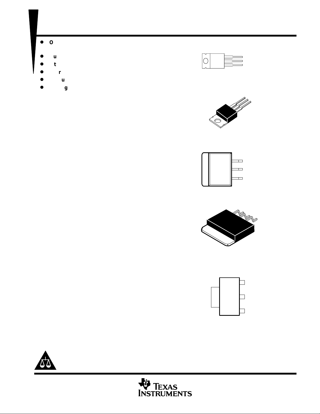
KC PACKAGE
(TOP VIEW)
INPUT
OUTPUT
ADJUST
The OUTPUT terminal is in electrical
contact with the mounting base.
TO-220AB
I
O
A
KTE PACKAGE
(TOP VIEW)
INPUT
OUTPUT
ADJUST
The OUTPUT terminal is in electrical
contact with the mounting base.
I
O
A
The LM317 is versatile in its applications,
including uses in programmable output regulation
and local on-card regulation. Or, by connecting a
fixed resistor between the ADJUST and OUTPUT
terminals, the LM317 can function as a precision
current regulator. An optional output capacitor can
be added to improve transient response. The
ADJUST terminal can be bypassed to achieve
very high ripple-rejection ratios, which are difficult
to achieve with standard three-terminal
regulators.
The LM317 is characterized for operation over the
virtual junction temperature range of 0°C to
125°C.
Please be aware that an important notice concerning availability, standard warranty, and use in critical applications of
Texas Instruments semiconductor products and disclaimers thereto appears at the end of this data sheet.
PRODUCTION DATA information is current as of publication date.
Products conform to specifications per the terms of Texas Instruments
standard warranty. Production processing does not necessarily include
testing of all parameters.
DCY PACKAGE
(TOP VIEW)
INPUT
OUTPUT
ADJUST
Copyright 2001, Texas Instruments Incorporated
POST OFFICE BOX 655303 • DALLAS, TEXAS 75265
1
Page 2

LM317
3-TERMINAL ADJUSTABLE REGULATOR
SLVS044H – SEPTEMBER 1997 – REVISED DECEMBER 2001
AVAILABLE OPTIONS
†
‡
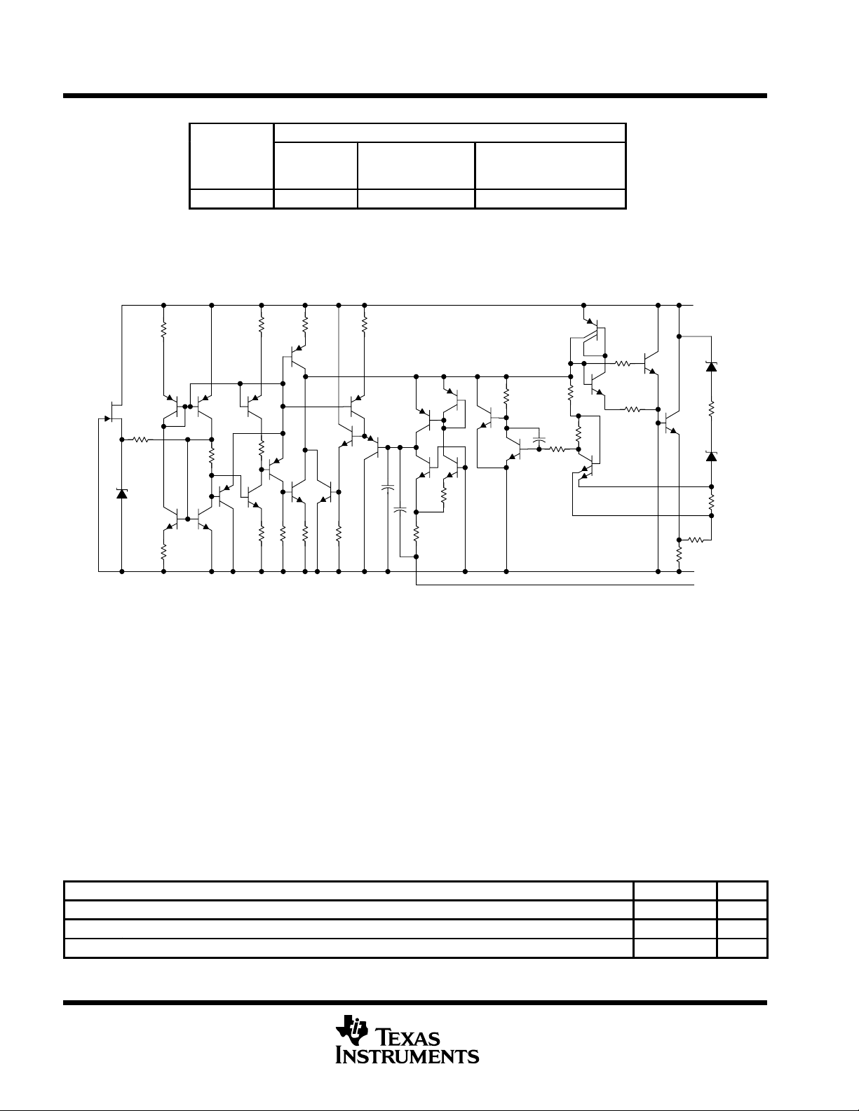
schematic diagram
T
J
0°C to 125°C LM317DCY LM317KC LM317KTER
The DCY package also is available taped and reeled, e.g., LM317DCYR.
The KTE package has the same footprint as TO-263 and can be mounted on a TO-263
land pattern. The KTE package is only available taped and reeled.
HEAT-SINK
(DCY)
†
MOUNTED, TO-220
PACKAGED DEVICES
HEAT-SINK
MOUNTED, POWER FLEX
(KC)
PLASTIC FLANGE
‡
(KTE)
INPUT
OUTPUT
ADJUST
absolute maximum ratings over virtual junction temperature range (unless otherwise noted)
Input-to-output differential voltage, V
Package thermal impedance, θ
– VO 40 V. . . . . . . . . . . . . . . . . . . . . . . . . . . . . . . . . . . . . . . . . . . . . . . . . . . .
I
(see Notes 1 and 2): DCY package 49°C/W. . . . . . . . . . . . . . . . . . . . . . . . .
JA
§
(see Notes 1 and 3): KC package 25°C/W. . . . . . . . . . . . . . . . . . . . . . . . . . .
(see Notes 1 and 2): KTE package 23°C/W. . . . . . . . . . . . . . . . . . . . . . . . .
Lead temperature 1,6 mm (1/16 inch) from case for 10 seconds 260°C. . . . . . . . . . . . . . . . . . . . . . . . . . . . . . .
Storage temperature range, T
§
Stresses beyond those listed under “absolute maximum ratings” may cause permanent damage to the device. These are stress ratings only, and
functional operation of the device at these or any other conditions beyond those indicated under “recommended operating conditions” is not
implied. Exposure to absolute-maximum-rated conditions for extended periods may affect device reliability.
NOTES: 1. Maximum power dissipation is a function of TJ(max), θJA, and TA. The maximum allowable power dissipation at any allowable
ambient temperature is PD = (TJ(max) – TA)/θJA. Operating at the absolute maximum TJ of 150°C can affect reliability.
2. The package thermal impedance is calculated in accordance with JESD 51-5.
3. The package thermal impedance is calculated in accordance with JESD 51-7.
–65°C to 150°C. . . . . . . . . . . . . . . . . . . . . . . . . . . . . . . . . . . . . . . . . . . . . . . . . . .
stg
recommended operating conditions
MIN MAX UNIT
VI – VOInput-to-output voltage differential 3 37 V
I
O
T
J
Output current 1.5 A
Operating virtual junction temperature 0 125 °C
2
POST OFFICE BOX 655303 • DALLAS, TEXAS 75265
Page 3

LM317
I
(line)
‡
V
V
3 V to 40 V
%/V
ADJ
µ ,
g
I
10 mA to 1500 mA
T
0°C to 125°C
Peak output current
A
Ripple rejection
V
10 V
f
120 HZ
dB
3-TERMINAL ADJUSTABLE REGULATOR
SLVS044H – SEPTEMBER 1997 – REVISED DECEMBER 2001
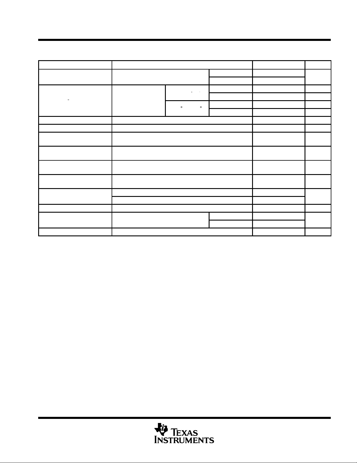
electrical characteristics over recommended ranges of operating virtual junction temperature
(unless otherwise noted)
PARAMETER
–
nput voltage
Output voltage
(load) regulation
Thermal regulation 20-ms pulse, TJ = 25°C 0.03 0.07 %VO/W
ADJUST terminal current 50 100 µA
Change in
ADJUST terminal current
Reference voltage (V
(OUTPUT to ADJUST)
Output-voltage
temperature stability
Minimum load current
to maintain regulation
p
Output noise voltage (RMS) f = 10 HZ to 10 kHZ, TJ = 25°C 0.003 %V
pp
Long-term stability TJ = 25°C 0.3 1 %/1k Hrs
†
Unless otherwise noted, the following test conditions apply: |VI – VO| = 5 V and I
used to maintain the junction temperature as close to the ambient temperature as possible.
‡
Input regulation is expressed here as the percentage change in output voltage per 1-V change at the input.
§
C
is connected between the ADJUST terminal and GND.
ADJ
NOTE 4: Maximum power dissipation is a function of TJ(max), θJA, and TA. The maximum allowable power dissipation at any allowable ambient
temperature is PD = (TJ(max) – TA)/θJA. Operating at the absolute maximum TJ of 150°C can affect reliability.
regulation
)
ref
=
I
O
=
O
VI – VO = 2.5 V to 40 V, PD ≤ 20 W , IO = 10 mA to 1500 mA 0.2 5 µA
VI – VO = 3 V to 40 V, PD ≤ 20 W , IO = 10 mA to 1500 mA 1.2 1.25 1.3 V
TJ = 0°C to 125°C 0.7 %V
VI – VO = 40 V 3.5 10 mA
VI – VO ≤ 15 V, PD < P
VI – VO ≤ 40 V, PD < P
,
=
O
TEST CONDITIONS
C
= 10 µF§,
TJ = 25°C
=
J
MAX
(see Note 1), TJ = 25°C 0.15 0.4
MAX
=
†
TJ = 25°C 0.01 0.04
TJ = 0°C to 125°C 0.02 0.07
VO ≤ 5 V 25 mV
VO ≥ 5 V 0.1 0.5 %V
VO ≤ 5 V 20 70 mV
VO ≥ 5 V 0.3 1.5 %V
(see Note 1) 1.5 2.2
= 0 µF
= 10 µF
§
§
C
ADJ
C
ADJ
= 1.5 A, TJ = 0°C to 125°C. Pulse testing techniques are
OMAX
MIN TYP MAX UNIT
57
62 64
O
O
O
O
POST OFFICE BOX 655303 • DALLAS, TEXAS 75265
3
Page 4

LM317
3-TERMINAL ADJUSTABLE REGULATOR
SLVS044H – SEPTEMBER 1997 – REVISED DECEMBER 2001
APPLICATION INFORMATION
V
I
INPUT
LM317
OUTPUT
V
O
ADJUST
V
= 1.25 V
I
Cin (Note A)
0.1 µF
NOTES: A. Cin is not required if the regulator is close enough to the power-supply filter.
V
out
Since I
B. CO improves transient response, but is not needed for stability.
is calculated as:
V
+
V
out
ref
is typically 50 µA, it is negligible in most applications.
Adj
R2
ǒ
1
)
R1
Ǔ
)
(I
R2)
Adj
Adj
ref
R2
Figure 1. Adjustable Voltage Regulator
LM317
+35 V
INPUT
OUTPUT
ADJUST
R1
120 Ω
R1
240 Ω
V
O
CO (Note B)
1.0 µF
V
is calculated as:
out
V
out
Since I
Adj
4
C1
0.1 µF
R2)R3
ǒ
+
V
1
)
ref
is typically 50 µA, it is negligible in most applications.
R1
Ǔ
)
I
(R2)R3) – 10 V
Adj
Figure 2. 0-V to 30-V Regulator Circuit
POST OFFICE BOX 655303 • DALLAS, TEXAS 75265
–10 V
R3
680 Ω
R2
3 kΩ
Page 5

LM317
3-TERMINAL ADJUSTABLE REGULATOR
SLVS044H – SEPTEMBER 1997 – REVISED DECEMBER 2001
APPLICATION INFORMATION
LM317
C3
1 µF
V
O
V
I
INPUT
C1
0.1 µF
OUTPUT
ADJUST
R1
240 Ω
D1
1N4002
(see Note A)
R2
5 kΩ
NOTE A: D1 discharges C2 if the output is shorted to ground.
Figure 3. Adjustable Regulator Circuit With Improved Ripple Rejection
LM317
V
I
OUTPUTINPUT
ADJUST
Figure 4. Precision Current-Limiter Circuit
ADJUST
V
I
INPUT
C1
0.1 µF
OUTPUT
LM317
C2
10 µF
R1
240 Ω
C2
1 µF
R1
INPUT
R2
720 Ω
LM317
OUTPUT
ADJUST
I
limit
Output
Adjust
1.2
+
R1
V
O
R3
120 Ω
R4
1 kΩ
Figure 5. Tracking Preregulator Circuit
POST OFFICE BOX 655303 • DALLAS, TEXAS 75265
5
Page 6

LM317
3-TERMINAL ADJUSTABLE REGULATOR
SLVS044H – SEPTEMBER 1997 – REVISED DECEMBER 2001
APPLICATION INFORMATION
V
Figure 6. 1.2-V to 20-V Regulator Circuit With Minimum Program Current
INPUT
I
LM317
OUTPUT
ADJUST
V
R1
1.2 kΩ
R2
20 kΩ
O
LM317
V
†
Minimum load current from each output is 10 mA. All output voltages are within 200 mV of each other.
INPUT OUTPUT
I
ADJUST
V
R1
120 Ω
†
V
O
I
R2
1 kΩ
LM317
INPUT OUTPUT
ADJUST
†
V
V
O
Figure 7. Adjusting Multiple On-Card Regulators With a Single Control
R
S
LM317
V
INPUT
I
OUTPUT
ADJUST
0.2 Ω
(see Note A)
R1
240 Ω
R2
2.4 kΩ
INPUT OUTPUT
I
LM317
ADJUST
†
V
O
NOTE A: RS controls the output impedance of the charger.
R2
Z
OUT
The use of RS allows for low charging rates with a fully charged battery.
ǒ
+
R
S
Ǔ
1
)
R1
Figure 8. Battery-Charger Circuit
6
POST OFFICE BOX 655303 • DALLAS, TEXAS 75265
Page 7

3-TERMINAL ADJUSTABLE REGULATOR
SLVS044H – SEPTEMBER 1997 – REVISED DECEMBER 2001
APPLICATION INFORMATION
LM317
LM317
V
INPUT
I
OUTPUT
ADJUST
24 Ω
Figure 9. 50-mA Constant-Current Battery-Charger Circuit
LM317
V
INPUT
I
2.7 kΩ
OUTPUT
ADJUST
R2
R1
240 Ω
2N2905
VO = 15 V
D1
1N4002
R3
50 kΩ
C1
25 µF
Figure 10. Slow Turn-On 15-V Regulator Circuit
12 V
I(PP)
LM317
V
V
INPUT
I
INPUT
I
OUTPUT
ADJUST
ADJUST
OUTPUT
LM317
480 Ω
120 Ω
Figure 11. AC Voltage-Regulator Circuit
120 Ω
480 Ω
6 V
O(PP)
2 W (TYP)
POST OFFICE BOX 655303 • DALLAS, TEXAS 75265
7
Page 8

LM317
3-TERMINAL ADJUSTABLE REGULATOR
SLVS044H – SEPTEMBER 1997 – REVISED DECEMBER 2001
APPLICATION INFORMATION
V
I+
NOTE A: R3 sets the peak current (0.6 A for a 1-Ω resistor).
Figure 12. Current-Limited 6-V Charger Circuit
INPUT
V
I–
ADJUST
LM317
OUTPUT
R1
240 Ω
R2
1.1 kΩ
R3
(see Note A)
LM317
V
I
INPUT
INPUT
INPUT
2N2905
OUTPUT
ADJUST
LM317
OUTPUT
ADJUST
LM317
OUTPUT
ADJUST
100 Ω
200 pF
TL080
_
+
0.2 Ω
0.2 Ω
4.5 V to 25 V
0.2 Ω
5 kΩ
5 kΩ
150 Ω
1.5 kΩ
Figure 13. Adjustable 4-A Regulator Circuit
8
POST OFFICE BOX 655303 • DALLAS, TEXAS 75265
Page 9

3-TERMINAL ADJUSTABLE REGULATOR
SLVS044H – SEPTEMBER 1997 – REVISED DECEMBER 2001
APPLICATION INFORMATION
TIP73
LM317
2N2905
V
I
22 Ω
10 µF
NOTES: A. The minimum load current is 30 mA.
B. This optional capacitor improves ripple rejection.
5 kΩ
Figure 14. High-Current Adjustable Regulator Circuit
INPUT
LM317
OUTPUT
ADJUST
120 Ω
10 µF
(see Note B)
500 Ω
1N4002
See
Note A
V
47 µF
O
POST OFFICE BOX 655303 • DALLAS, TEXAS 75265
9
Page 10

IMPORTANT NOTICE
Texas Instruments Incorporated and its subsidiaries (TI) reserve the right to make corrections, modifications,
enhancements, improvements, and other changes to its products and services at any time and to discontinue
any product or service without notice. Customers should obtain the latest relevant information before placing
orders and should verify that such information is current and complete. All products are sold subject to TI’s terms
and conditions of sale supplied at the time of order acknowledgment.
TI warrants performance of its hardware products to the specifications applicable at the time of sale in
accordance with TI’s standard warranty . Testing and other quality control techniques are used to the extent TI
deems necessary to support this warranty . Except where mandated by government requirements, testing of all
parameters of each product is not necessarily performed.
TI assumes no liability for applications assistance or customer product design. Customers are responsible for
their products and applications using TI components. T o minimize the risks associated with customer products
and applications, customers should provide adequate design and operating safeguards.
TI does not warrant or represent that any license, either express or implied, is granted under any TI patent right,
copyright, mask work right, or other TI intellectual property right relating to any combination, machine, or process
in which TI products or services are used. Information published by TI regarding third–party products or services
does not constitute a license from TI to use such products or services or a warranty or endorsement thereof.
Use of such information may require a license from a third party under the patents or other intellectual property
of the third party , or a license from TI under the patents or other intellectual property of TI.
Reproduction of information in TI data books or data sheets is permissible only if reproduction is without
alteration and is accompanied by all associated warranties, conditions, limitations, and notices. Reproduction
of this information with alteration is an unfair and deceptive business practice. TI is not responsible or liable for
such altered documentation.
Resale of TI products or services with statements different from or beyond the parameters stated by TI for that
product or service voids all express and any implied warranties for the associated TI product or service and
is an unfair and deceptive business practice. TI is not responsible or liable for any such statements.
Mailing Address:
Texas Instruments
Post Office Box 655303
Dallas, Texas 75265
Copyright 2001, Texas Instruments Incorporated
 Loading...