

Page 1
User's Guide
SLOU403C–March 2015–Revised June 2018
DRV2700EVM High Voltage Piezo Driver Evaluation Kit
The DRV2700 is a single-chip, high-voltage piezo driver with an integrated 105-V boost switch, integrated
power diode, and integrated fully differential amplifier. This evaluation kit demonstrates:
• Multiple input modes including: 0- to 10-V single ended, PWM, and AC input modes
• Multiple output modes including: 0- to 200-Vpp differential, 0- to 105-V single and multiple ended
• 2 power supply inputs to isolate power consumption on DRV2700
• 8 convenient boost voltage settings and 4 different gain settings
• Small footprint (9 mm x 13 mm)
• Breakout for usage as a boost converter
The evaluation kit is designed for all-around use and can be used not only for evaluation but can also be
used for prototyping into systems. The EVM also contains a microcontroller, LDO (3.3 V) and LEDs for
status and input settings.
Evaluation Kit Contents:
• DRV2700EVM evaluation board
• Demonstration mode firmware preloaded onto microcontroller
• Downloadable software to control EVM
• Mini-B USB cable
Needed for programming and advanced configuration:
• Code Composer Studio™ (CCS) or IAR Embedded Workbench IDE for MSP430
• MSP430 LaunchPad™ (MSP-EXP430G2) or MSP430-FET430UIF hardware programming tool
• DRV2700EVM firmware available on the DRV2700EVM tool folder
• MSP-JTAG2SBW JTAG to Spy-Bi-Wire adapter
SLOU403C–March 2015–Revised June 2018
Submit Documentation Feedback
DRV2700EVM High Voltage Piezo Driver Evaluation Kit
Copyright © 2015–2018, Texas Instruments Incorporated
1
Page 2

www.ti.com
Contents
1 Getting Started ............................................................................................................... 6
1.1 Evaluation Module Operating Parameters....................................................................... 6
1.2 Quick Start Board Setup ........................................................................................... 7
1.3 Connecting a Load.................................................................................................. 7
2 Overview of EVM ............................................................................................................ 8
2.1 DRV2700............................................................................................................. 8
2.2 Microcontroller (MSP430).......................................................................................... 8
2.3 Power Supply Inputs and Path.................................................................................... 8
2.4 EN and Gain Configuration........................................................................................ 9
2.5 Inputs ............................................................................................................... 10
2.6 Outputs ............................................................................................................. 10
2.7 BST/PVDD Disconnect ........................................................................................... 10
2.8 TRIG Button........................................................................................................ 10
3 EVM Control Software (GUI).............................................................................................. 11
4 Boost Converter ............................................................................................................ 12
4.1 Boost Voltage Setting Resistors................................................................................. 13
4.2 Disconnecting BST/PVDD........................................................................................ 14
4.3 Programming the Boost Current Limit.......................................................................... 14
4.4 Boost Inductor Selection ......................................................................................... 14
4.5 Boost Capacitor Selection........................................................................................ 14
5 PWM, Analog, and Single-Ended Inputs................................................................................ 15
5.1 PWM (AC Coupled) Input Using MSP430 ..................................................................... 15
5.2 PWM (AC Coupled) Input Using AIN ........................................................................... 15
5.3 External Analog (AC Coupled) Input............................................................................ 16
5.4 Single-Ended (DC Coupled) Input .............................................................................. 16
6 Output........................................................................................................................ 19
6.1 Two Terminal Differential Output Configuration (OUT+ – OUT–)........................................... 19
6.2 Two Terminal Single Ended Output Configuration (OUT± to BST/GND).................................. 19
6.3 Three Terminal Single Ended Output Configuration (BST to OUT± to GND)............................. 20
7 Load Selection.............................................................................................................. 20
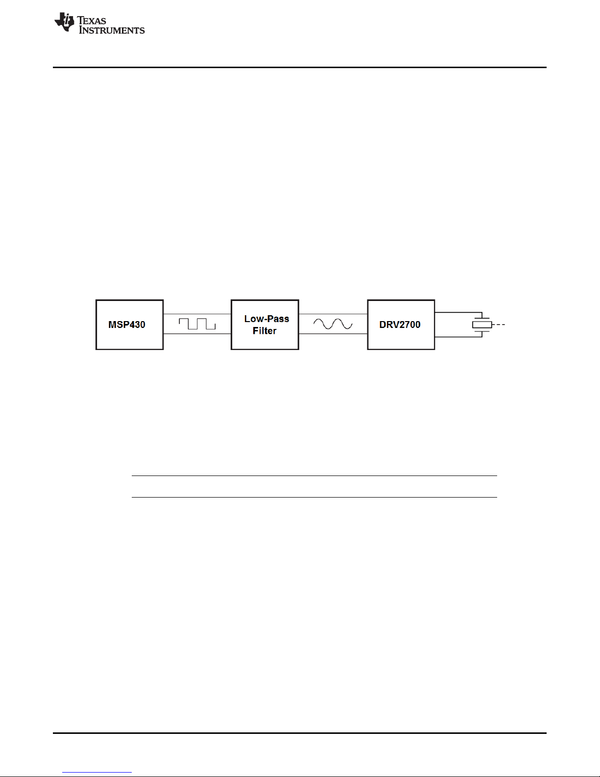
8 Filtering and Adapting PWM Waveforms................................................................................ 21
8.1 PWM Input ......................................................................................................... 21
8.2 Filter Selection Criteria ........................................................................................... 22
9 Reference ................................................................................................................... 25
9.1 Schematic .......................................................................................................... 25
9.2 PCB Layout ........................................................................................................ 26
9.3 Bill of Materials .................................................................................................... 28
1 Board Diagram ............................................................................................................... 6
2 Power Path Diagram ........................................................................................................ 8
3 Gain = 40.7 dB............................................................................................................... 9
4 Gain = 38.4 dB............................................................................................................... 9
5 Gain = 34.8 dB............................................................................................................... 9
6 Gain = 28.8 dB............................................................................................................... 9
7 GUI Interface................................................................................................................ 11
8 BST Network JP2, JP3, and JP4......................................................................................... 13
9 PWM Signal................................................................................................................. 15
10 Set Reference to External 2.5 V ......................................................................................... 17
11 Floating Reference at 3 Hz and No Load............................................................................... 17
12 Floating Reference at 1 Hz and No Load............................................................................... 17
13 DC Coupled Input Diagram ............................................................................................... 18
2
DRV2700EVM High Voltage Piezo Driver Evaluation Kit
List of Figures
Copyright © 2015–2018, Texas Instruments Incorporated
SLOU403C–March 2015–Revised June 2018
Submit Documentation Feedback
Page 3

www.ti.com
14 Two Terminal Differential Output......................................................................................... 19
15 Two Terminal Single Ended Output ..................................................................................... 19
16 Three Terminal Single Ended Output ................................................................................... 20
17 DRV2700EVM First- and Second-Order Filters........................................................................ 21
18 Differential, First-Order Filter ............................................................................................. 22
19 Frequency Response of the First-Order Filter.......................................................................... 22
20 Differential, Second-Order Filter ......................................................................................... 23
21 Frequency Response of the Second-Order Filter...................................................................... 23
22 DRV2700EVM Schematic................................................................................................. 25
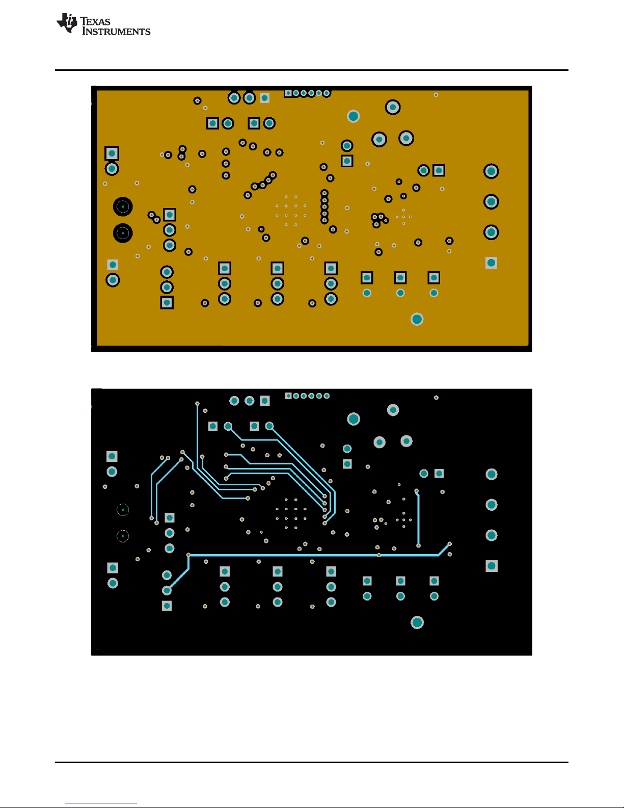
23 All Layers.................................................................................................................... 26
24 Top Layer ................................................................................................................... 26
25 Mid Layer 1 ................................................................................................................. 27
26 Mid Layer 2 ................................................................................................................. 27
27 Bottom Layer................................................................................................................ 28
WARNING
EXPORT NOTICE
Recipient agrees to not knowingly export or re-export, directly or
indirectly, any product or technical data (as defined by the U.S.,
EU, and other Export Administration Regulations) including
software, or any controlled product restricted by other applicable
national regulations, received from Disclosing party under this
Agreement, or any direct product of such technology, to any
destination to which such export or re-export is restricted or
prohibited by U.S. or other applicable laws, without obtaining prior
authorization from U.S. Department of Commerce and other
competent Government authorities to the extent required by those
laws. This provision shall survive termination or expiration of this
Agreement. According to our best knowledge of the state and enduse of this product or technology, and in compliance with the
export control regulations of dual-use goods in force in the origin
and exporting countries, this technology is classified as follows:
US ECCN: 3E991
EU ECCN: EAR99
And may require export or re-export license for shipping it in
compliance with the applicable regulations of certain countries.
SLOU403C–March 2015–Revised June 2018
Submit Documentation Feedback
DRV2700EVM High Voltage Piezo Driver Evaluation Kit
Copyright © 2015–2018, Texas Instruments Incorporated
3
Page 4
www.ti.com
Cautions and Warnings
CAUTION:
Warning! Do not leave EVM powered when unattended.
HOT SURFACE:
Warning Hot Surface! Contact may cause burns. Do not touch. Please take the proper
precautions when operating.
HIGH VOLTAGE:
Danger High Voltage! Electric shock possible when connecting board to live wire. Board should
be handled with care by a professional. For safety, use of isolated test equipment with
overvoltage/overcurrent protection is highly recommended.
4
DRV2700EVM High Voltage Piezo Driver Evaluation Kit
Copyright © 2015–2018, Texas Instruments Incorporated
SLOU403C–March 2015–Revised June 2018
Submit Documentation Feedback
Page 5

WARNING
www.ti.com
General Texas Instruments High Voltage Evaluation (TI HV EVM) User Safety Guidelines
Always follow TI’s setup and application instructions, including use of all interface components within their
recommended electrical rated voltage and power limits. Always use electrical safety precautions to help
ensure your personal safety and those working around you. Contact TI's Product Information Center
http://support/ti./com for further information.
Save all warnings and instructions for future reference.
Failure to follow warnings and instructions may result in personal injury, property damage, or
death due to electrical shock and burn hazards.
The term TI HV EVM refers to an electronic device typically provided as an open framed, unenclosed
printed circuit board assembly. It is intended strictly for use in development laboratory environments,
solely for qualified professional users having training, expertise and knowledge of electrical safety
risks in development and application of high voltage electrical circuits. Any other use and/or
application are strictly prohibited by Texas Instruments. If you are not suitable qualified, you should
immediately stop from further use of the HV EVM.
1. Work Area Safety
1. Keep work area clean and orderly.
2. Qualified observer(s) must be present anytime circuits are energized.
3. Effective barriers and signage must be present in the area where the TI HV EVM and its interface
electronics are energized, indicating operation of accessible high voltages may be present, for the
purpose of protecting inadvertent access.
4. All interface circuits, power supplies, evaluation modules, instruments, meters, scopes and other
related apparatus used in a development environment exceeding 50Vrms/75VDC must be
electrically located within a protected Emergency Power Off EPO protected power strip.
5. Use stable and nonconductive work surface.
6. Use adequately insulated clamps and wires to attach measurement probes and instruments. No
freehand testing whenever possible.
2. Electrical Safety
As a precautionary measure, it is always a good engineering practice to assume that the entire EVM
may have fully accessible and active high voltages.
1. De-energize the TI HV EVM and all its inputs, outputs and electrical loads before performing any
electrical or other diagnostic measurements. Revalidate that TI HV EVM power has been safely
de-energized.
2. With the EVM confirmed de-energized, proceed with required electrical circuit configurations,
wiring, measurement equipment connection, and other application needs, while still assuming the
EVM circuit and measuring instruments are electrically live.
3. After EVM readiness is complete, energize the EVM as intended.
WARNING: WHILE THE EVM IS ENERGIZED, NEVER TOUCH THE EVM OR ITS ELECTRICAL
CIRCUITS AS THEY COULD BE AT HIGH VOLTAGES CAPABLE OF CAUSING ELECTRICAL
SHOCK HAZARD.
3. Personal Safety
1. Wear personal protective equipment (for example, latex gloves or safety glasses with side shields)
or protect EVM in an adequate lucent plastic box with interlocks to protect from accidental touch.
Limitation for safe use:
EVMs are not to be used as all or part of a production unit.
SLOU403C–March 2015–Revised June 2018
Submit Documentation Feedback
DRV2700EVM High Voltage Piezo Driver Evaluation Kit
Copyright © 2015–2018, Texas Instruments Incorporated
5
Page 6
Getting Started
1 Getting Started
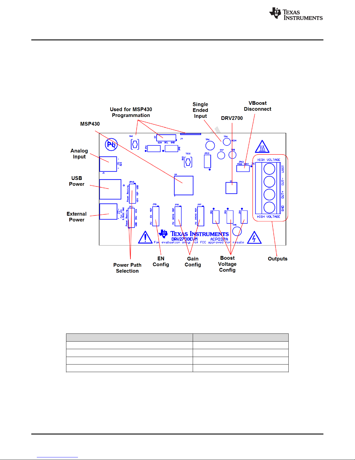
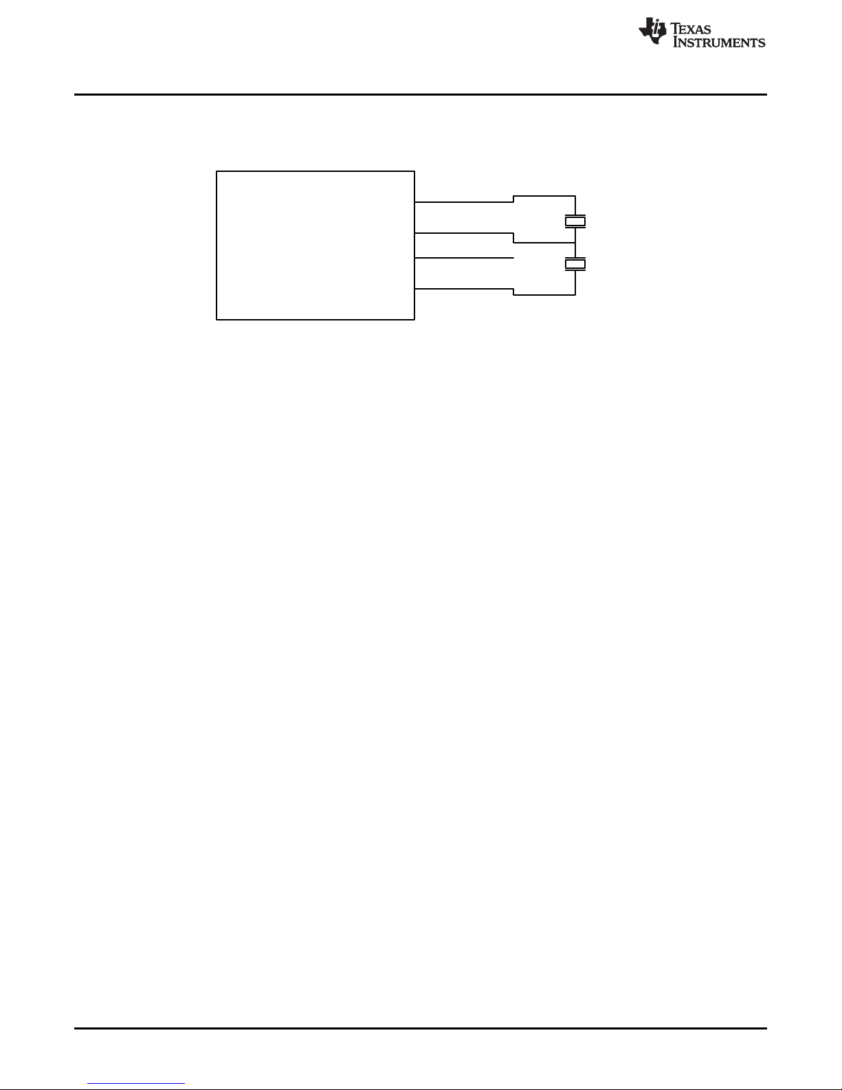
The DRV2700EVM is designed for flexible use for prototyping as well as evaluation. Figure 1 shows the
names and locations of the various elements on the EVM. To power the board, connect the DRV2700EVM
to an available USB port on your computer using a mini-B USB cable. The default board settings cause
the microcontroller (MSP430) to control the inputs of the DRV2700 at power up. The MSP430 has each of
these control settings low which disables the DRV2700, by default. Figure 1 shows the basic board
diagram of the DRV2700EVM. Table 2 shows the original configuration of the jumpers, as shipped.
www.ti.com
1.1 Evaluation Module Operating Parameters
Table 1 lists the operating conditions for the DRV2700 on the evaluation module.
Parameter Specification
Supply voltage range 3.6 V to 5.5 V
Power-supply current rating 500 mA
Input Voltage 0 V to V
Max Output Voltage 200 Vpp
6
DRV2700EVM High Voltage Piezo Driver Evaluation Kit
Figure 1. Board Diagram
Table 1. Typical Operating Conditions
Copyright © 2015–2018, Texas Instruments Incorporated
DD
SLOU403C–March 2015–Revised June 2018
Submit Documentation Feedback
Page 7
www.ti.com
1.2 Quick Start Board Setup
The DRV2700EVM comes with preprogrammed firmware to provide a 0- to 200-Vpp signal between OUT+
and OUT–.
1. Out of the box, the jumpers are set to begin demo mode using USB power. The default jumper settings
are found in Table 2.
2. Connect a mini-USB cable to the USB connector on the DRV2700EVM board.
3. Connect the other end of the USB cable to an available USB port on a computer, USB charger, or USB
battery pack.
4. If the board is powered correctly, the 5-V LED is on.
5. Enable the output using the GUI or programmatically through the computer, see GUI Interface for
additional assistance. If using an external input signal, EN the output by changing the jumper (JP9) or
equivalent control signal.
6. Once the output is EN, the device allows for the high-voltage output.
Parameter Jumper Setting Default Specification
Open MSP not connected to either power supply
JP10 MSP
JP11 DRV
JP5 and JP6
JP9-EN
JP8-G1
JP7-G0
JP13-DCIN
JP12-VBST
I2C Open Always leave open. Never jumper together.
J2, J3, J4
(1)
In the table, (top) or (bottom) means the (top) or (bottom) is connected to the middle of the 3-terminal header. For questions,
refer to Figure 1.
USB (top)
VIN (bottom)
Open DRV2700 not connected to either power supply
VIN (top)
USB (bottom)
Open Disconnected PWM± and I/O of MSP430
Connected X Connected PWM± and I/O of MSP430
Open EN/G1/G0 pulled internally to GND through DRV2700 internal resistance
MSP (top)
PU (bottom)
Open X DC input not connected (PWM and AC input mode)
Connected DC input connected (single-ended input mode)
Open PVDD disconnected to BST (boost only mode)
Connected X PVDD connected to BST (normal operation)
Open Disconnects particular FB resistor (lowers BST)
Connected X Connects particular FB resistor (raises BST)
(1)
(1)
(1)
(1)
(1)
(1)
Getting Started
Table 2. Default Jumper Settings
X MSP connected to USB power supply
MSP connected to VIN power supply
DRV2700 connected to VIN power supply
X DRV2700 connected to USB power supply
X EN/G1/G0 tied to I/O of MSP430
EN/G1/G0 pulled up to MSP power supply through external pull up resistor
1.3 Connecting a Load
1. With the power supply off, connect the negative terminal of the load to OUT– and connect the positive
terminal of the load to OUT+
2. Ensure the terminals are connected correctly, then enable the supply
Before connecting the load, ensure that the load is rated for the
selected output voltage. If not, see the Boost Voltage Setting
Resistors section to adjust the DRV2700 maximum output voltage.
See Figure 13 for a diagram of the input configuration.
SLOU403C–March 2015–Revised June 2018
Submit Documentation Feedback
WARNING
DRV2700EVM High Voltage Piezo Driver Evaluation Kit
Copyright © 2015–2018, Texas Instruments Incorporated
7
Page 8
USB
Power
VIN
External
MSP HeaderDRV Header
Power to Rest of Board
Power to DRV2700
Overview of EVM
2 Overview of EVM
The following sections provide a description of each of the blocks identified in Figure 1.
2.1 DRV2700
The DRV2700 is a single-chip, high-voltage piezo driver with an integrated 105-V boost switch, integrated
power diode, and integrated fully-differential amplifier. This EVM allows the designer to evaluate this
device and appropriately prototype it into their design. See the DRV2700 (SLOS861) datasheet for more
in-depth information.
2.2 Microcontroller (MSP430)
An onboard MSP430F5510 is used to control the various input signals as well as communicate through
the USB to the GUI. See the Quick Start Board Setup section for how to setup and run with the GUI.
2.3 Power Supply Inputs and Path
Two power supply inputs are available to power the EVM: USB power and V
Each of these inputs can be used to power the entire board or parts of the board.
2.3.1 USB Power Input
The USB power input can be supplied from a standard USB port on a computer, USB charger, or USB
battery pack. This input is intended for ease-of-use and can be routed to power all circuitry on the EVM.
Additionally, this input has a 5-V LED indicator showing that power is being supplied to the EVM. If the
GUI is going to be used, the USB must be connected to the computer and JP10 routed to USB
connection.
EXTERNAL
www.ti.com
(Ext VIN on the EVM).
2.3.2 VIN/External Power Input
Provide the VIN power input with an external 3.6- to 5.5-V power supply. Additionally, this input can power
the entire board.
2.3.3 Power Path Selection
Each of the two power supply inputs can be routed to the DRV2700 or the rest of the IC. The positions of
the jumpers are described in Table 2 or can be read from the silkscreen of the EVM. Figure 2 shows the
basic diagram of the power paths.
If a power measurement of the DRV2700 circuitry is desired, it is best to provide the MSP jumper (JP10)
with USB power and the DRV jumper (JP11) with VIN. With this configuration, measuring the provided
voltage and current into VIN gives the power consumption of the DRV2700.
Figure 2. Power Path Diagram
8
DRV2700EVM High Voltage Piezo Driver Evaluation Kit
Copyright © 2015–2018, Texas Instruments Incorporated
SLOU403C–March 2015–Revised June 2018
Submit Documentation Feedback
Page 9
www.ti.com
2.4 EN and Gain Configuration
The EN, GAIN0, and GAIN1 inputs into the DRV2700 have 4 different driving configurations:
• Driven through the MSP430. This is done by connecting the configuration jumper to the “MSP” state
(default).
• Pulled to a logic level high through pullup resistor. This is done by connecting the configuration jumper
to the “PU” state.
• Pulled to a logic level low through internal pulldown resistor. This is done by removing the configuration
jumper.
• Driven externally. This is done by connecting the external control signal to the center 100-mil header.
Each of these signals have an LED to indicate when the signal is at a logic-level high.
Additionally, the GAIN pins control the internal gain of the high voltage amplifier. Table 3 shows the 4 gain
settings
GAIN1 GAIN0 Gain (dB)
Low Low 28.8
Low High 34.8
High Low 38.4
High High 40.7
Overview of EVM
Table 3. Gain Settings
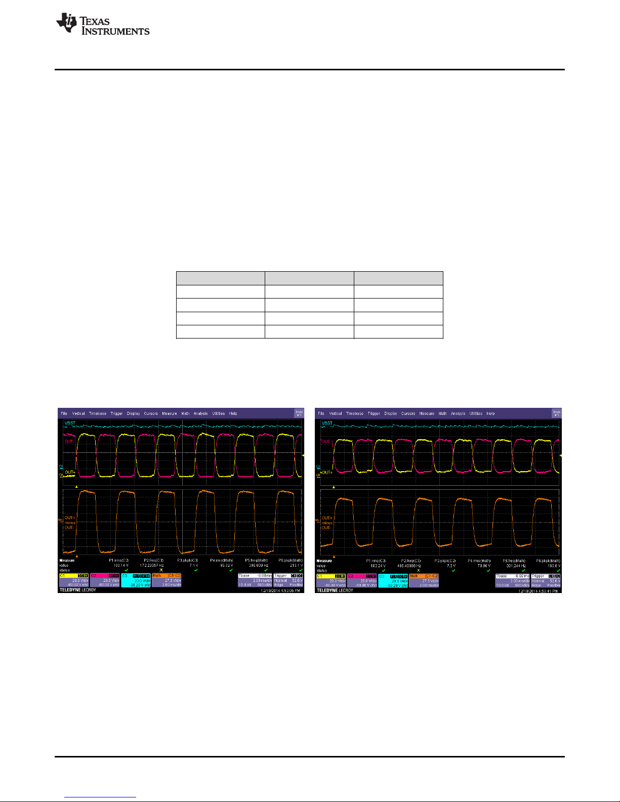
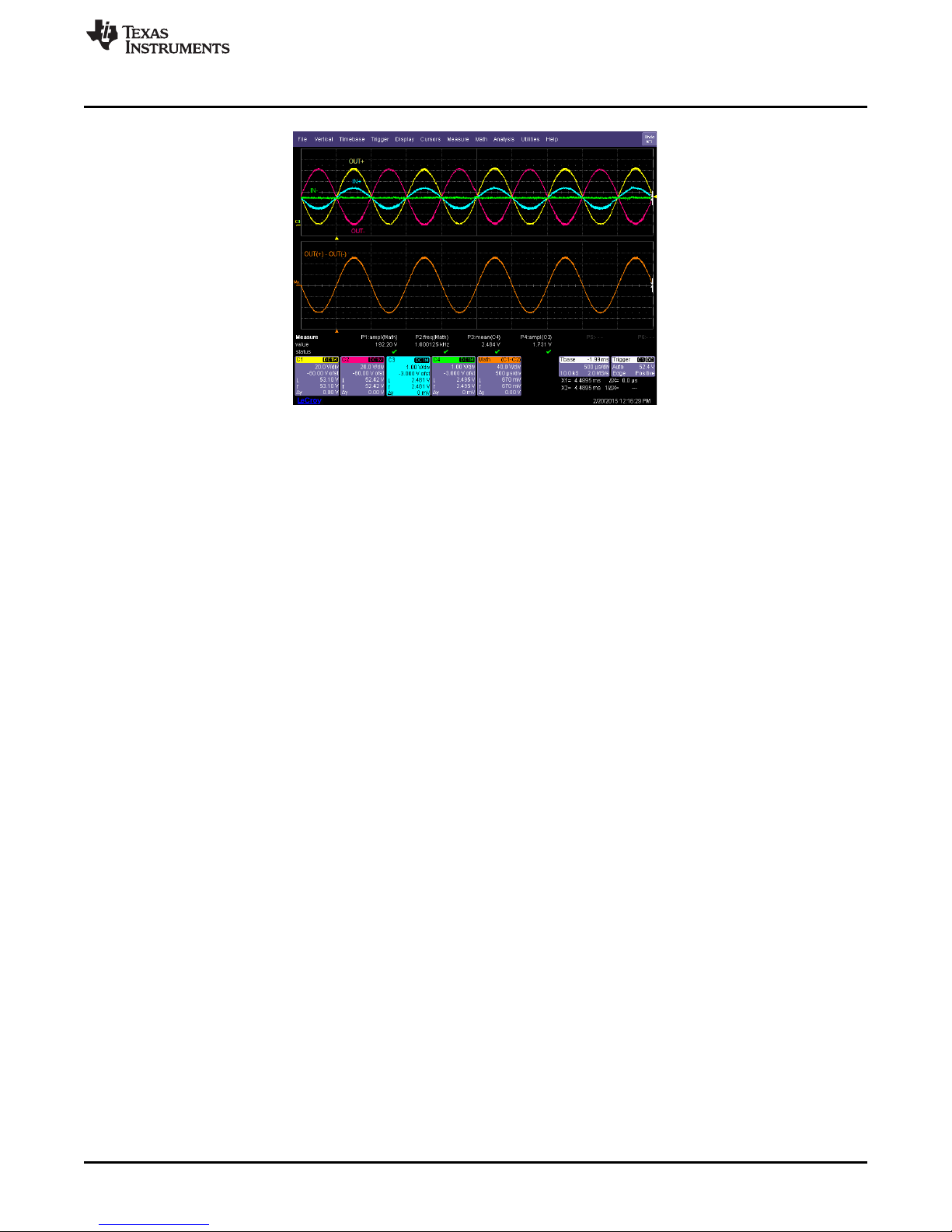
Figure 3 through Figure 6 showcase all 4 gain settings with BST set to max of 105 V (JP2, JP3, and JP4
closed). C3 = BST, C1 = VOUT(+), C2 = VOUT(–), and MATH = OUT(+) – OUT (–). PWM input from
MSP430 of 0–3.3 V, 300 Hz and 50% duty cycle.
Figure 3. Gain = 40.7 dB Figure 4. Gain = 38.4 dB
SLOU403C–March 2015–Revised June 2018
Submit Documentation Feedback
DRV2700EVM High Voltage Piezo Driver Evaluation Kit
Copyright © 2015–2018, Texas Instruments Incorporated
9
Page 10
Overview of EVM
2.5 Inputs
The analog input (AIN) is used for PWM and analog inputs. The single-ended (DC) input test point is used
when a DC input is desired. See PWM, Analog, and Single-Ended Inputs, for more information.
www.ti.com
Figure 5. Gain = 34.8 dB Figure 6. Gain = 28.8 dB
2.6 Outputs
The DRV2700EVM has 4 referenced outputs (BST, OUT–, OUT+, and GND). They are output from a
terminal block to mitigate touching between two high voltage lines. See the Output section for additional
information.
2.7 BST/PVDD Disconnect
The BST jumper (JP12) is provided to allow disconnecting between PVDD and BST. This enables the
DRV2700EVM to be configured purely as a boost converter. See Disconnecting BST/PVDD, for additional
information.
2.8 TRIG Button
The DRV2700EVM has a built-in trigger button for user prototyping. If different modes of operation are
desired without using the GUI, the MSP430 can be programmed such that the trigger button can cycle
through different modes. Additionally, there are 3 test point pads that be can be used in a similar manner
through MSP430 firmware programming.
See Figure 13 for a diagram of the input configuration.
10
DRV2700EVM High Voltage Piezo Driver Evaluation Kit
Copyright © 2015–2018, Texas Instruments Incorporated
SLOU403C–March 2015–Revised June 2018
Submit Documentation Feedback
Page 11
Gain Settings
and Boost Chart
EN Output
Output
Timing
Output
Status
Standard Drive
vs Audio Drive
Frequency
Control
Duty Cycle
Control
Note
and/or
Frequency
Generator
Simple
Piano
www.ti.com
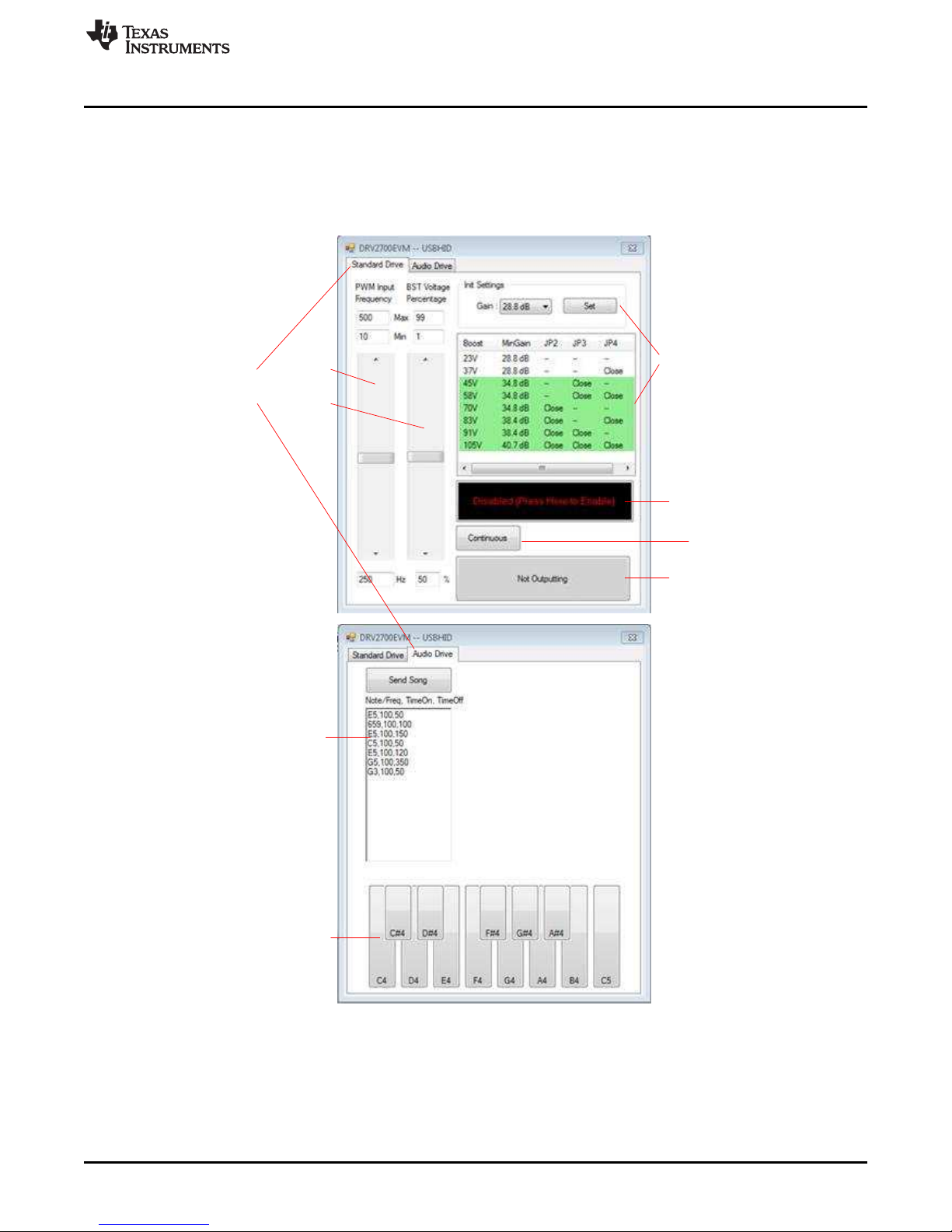
3 EVM Control Software (GUI)
By default, the DRV2700EVM can be controlled programmatically through the GUI Interface. Figure 7 is a
screenshot of the GUI.
Run the GUI by downloading it from the DRV2700 product page, installing the GUI and then running it.
When prompted, connect to the USBHID setting.
EVM Control Software (GUI)
Figure 7. GUI Interface
SLOU403C–March 2015–Revised June 2018
Submit Documentation Feedback
DRV2700EVM High Voltage Piezo Driver Evaluation Kit
Copyright © 2015–2018, Texas Instruments Incorporated
11
Page 12

Boost Converter
The GUI is broken up into two sections: Standard Drive and Audio Drive. The Standard Drive utilizes
changing the frequency and duty cycle of the PWM signal and is intended for easy prototyping. The Audio
Drive tab is for showcasing the DRV2700 as a Piezo buzzer/speaker. On both tabs, the sections are
intuitive, however, the following sections are worth describing:
• Gain Settings and Boost Chart: After changing the gain and clicking the Set button, the MSP430
changes the G0 and G1 GPIO therefore changing the gain of the DRV2700. The chart then updates to
reflect the recommended voltage ranges by not highlighting them.
• Output Timing: This button has 3 different modes: Continuous, Pulsed, and Single. These modes help
with a timed EN signal.
• Duty Cycle: This allows control of the power that gets through the DC blocking input filter. Duty Cycle
can be thought of as an amplitude control. Additionally, the PWM signal can be connected through
external wires using JP5 and JP6 headers to IN+ and IN–, in order to control the output.
• Note Generator and Simple Piano: The DRV2700 is capable of also driving piezo loads used in
many alarms and buzzers. To sample this, the simple piano sends the corresponding frequency of the
notes when pressed. If a series of notes and/or frequencies with specific timing is desired, the note
generator can be used in the format of “[Note],[TimeOn],[TimeOff]” as shown in Figure 7. The note
format is A–G (including sharps “#” but not flats “b”) followed by the octave, and the frequency is in Hz
rounded to the nearest integer. Some examples include: A4, C#5, E5 (or 659), and so forth. All time
inputs are based in milliseconds.
See Figure 13 for a diagram of the input configuration.
4 Boost Converter
The DRV2700 device creates a boosted supply rail with an integrated DC-DC converter that can go up to
105 V. The switch-mode power supplies have a few different sources of losses. When boosting to very
high voltages, the efficiency begins to degrade because of these losses. The DRV2700 device has a
hysteretic boost design to minimize switching losses and therefore increase efficiency. A hysteretic
controller is a self-oscillation circuit that regulates the output voltage by keeping the output voltage within a
hysteresis window set by a reference voltage regulator and, in this case, the current-limit comparator.
Hysteretic converters typically have a larger ripple as a trade off because of the minimized switching. This
ripple is a function of the output capacitor, internal delays, and the hysteresis of the control loop. The
power FET and power diode of the boost converter are both integrated within the device to provide the
required switching while minimizing external components. Additionally, the boost voltage output (BST) can
be easily fed into the high-voltage amplifier through the adjacent pin (PVDD) to help minimize routing
inductance and resistance on the board.
Before connecting the load, ensure the load is rated for the current boost voltage setting.
See Boost Voltage Setting Resistors for more information on how to set the boost voltage.
www.ti.com
12
DRV2700EVM High Voltage Piezo Driver Evaluation Kit
Copyright © 2015–2018, Texas Instruments Incorporated
SLOU403C–March 2015–Revised June 2018
Submit Documentation Feedback
Page 13

æ ö
÷
ø
= +
ç
ç ÷
è
1
BST FB
EQ
R
V V 1
R
R
5
806 lQ
R
4
80.6 lQ
R
3
49.9 lQ
R
2
23.3 lQ
R
1
49.9 lQ
JP2JP3JP4
FB
BST
www.ti.com
4.1 Boost Voltage Setting Resistors
The boost voltage (BST) is set through a resistor network and through the use of jumpers JP2, JP3, and
JP4 as shown in Figure 8.
Figure 8. BST Network JP2, JP3, and JP4
The boost output voltage is given by Equation 1
where VFB= 1.32 V and REQis the equivalent resistor between all the connected resistors in parallel. Refer
to Table 4 for BST setting based on the jumper configuration.
Boost Converter
(1)
WARNING
Be sure not to hot switch the JP2, JP3, or JP4 connection. This can
be accomplished by only removing or connecting the JP2, JP3, or
JP4 jumpers while the board is unpowered.
Table 4. BST Setting Based on the Jumper Configuration
BST R
23 V 50 kΩ Open Open Open
37 V 30.8 kΩ Open Open Closed
45 V 25 kΩ Open Closed Open
58 V 19.0 kΩ Open Closed Closed
70 V 15.7 kΩ Closed Open Open
83 V 13.2 kΩ Closed Open Closed
91 V 12 kΩ Closed Closed Open
105 V 10.4 kΩ Closed Closed Closed
EQ
If another voltage is desired, replace R1 and R5 using Equation 1 and leave JP2–4 disconnected.
JP2 JP3 JP4
SLOU403C–March 2015–Revised June 2018
Submit Documentation Feedback
DRV2700EVM High Voltage Piezo Driver Evaluation Kit
Copyright © 2015–2018, Texas Instruments Incorporated
13
Page 14

REF
EXT INT
LIM
V
I
æ ö
= -
ç ÷
è ø
Boost Converter
4.2 Disconnecting BST/PVDD
The DRV2700 has two essential blocks: the boost converter and the amplifier. If only using the
DRV2700’s boost converter, JP_VBST allows the user to disconnect PVDD from BST to shut down the
amplifier to save power.
Be sure not to hot switch the BST and PVDD connection. This can
only be accomplished by removing or connecting the JP_VBST
jumper while the board is unpowered.
4.3 Programming the Boost Current Limit
The peak inductor current is set with resistor R3 (REXT). The current limit is not a safety mechanism, but
the highest value current the inductor will see each cycle. The inductor must be capable of handling this
programmed limit during normal operation. The relationship of REXT to ILIM is approximated with
Equation 2 where I
is the current limit set by R
LIM
4.4 Boost Inductor Selection
Inductor selection plays a critical role in the performance of the DRV2700. The range of recommended
inductor values is 3.3 µH to 22 µH. When a larger inductance is chosen, the DRV2700 boost converter
automatically runs at a lower switching frequency and incurs less switching losses; however, the larger
inductors may also have a higher equivalent series resistance (ESR), which will increase the parasitic
inductor losses. Smaller inductances generally have higher saturation currents; therefore, they are better
suited for maximizing the output current of the boost converter. Table 5 lists several sample inductors that
provide adequate performance.
WARNING
, K = 10500, V
EXT
= 1.35 V and R
REF
= 60 Ω.
INT
www.ti.com
(2)
Manufacturer Part Number DCR (Ω) Inductance (µH) I
Coilcraft LPS4018-332MLB 0.080 3.3 1.9 7.32k 1.9
Coilcraft LPS4018-472MLB 0.125 4.7 1.8 7.5k 1.8
TDK VLS3012T-3R3M1R3 0.100 3.3 1.5 9.31k 1.5
4.5 Boost Capacitor Selection
The boost output voltage may be programmed as high as 105 V. A capacitor must have a voltage rating
equivalent to the boost output voltage or higher. A 250-V rated 100-nF capacitor of X5R or X7R type is
recommended for a boost converter voltage of 105 V. The selected capacitor should have a minimum
derated capacitance of 50 nF.
See Figure 13 for a diagram of the input configuration.
Table 5. Sample Inductors
(A) R
SAT
(Ω) I
EXT
LIM
(A)
14
DRV2700EVM High Voltage Piezo Driver Evaluation Kit
Copyright © 2015–2018, Texas Instruments Incorporated
SLOU403C–March 2015–Revised June 2018
Submit Documentation Feedback
Page 15
www.ti.com
5 PWM, Analog, and Single-Ended Inputs
The DRV2700 requires a low-pass filtered PWM waveform, an analog signal or a single-ended input to
drive capacitive loads. By default, the DRV2700EVM uses the MSP430 PWM input mode with a low-pass
filter. This section describes each input mode in detail and the modifications necessary for operation of
each. See Filtering and Adapting PWM Waveforms for more details on adapting the PWM waveform using
a low-pass filter.
The DRV2700EVM supports four input modes for driving the DRV2700:
• PWM (AC coupled) input using MSP430: In this mode, the onboard MSP430 generates a PWM
waveform that is sent through the low-pass input filter to the DRV2700.
• PWM (AC coupled) input using AIN: An external source supplies a PWM waveform to the EXTIN
header which is sent through the low-pass input filter to the DRV2700.
• External analog (AC coupled) input: An external source supplies an analog waveform (sine wave) to
the IN+ and IN– header. The low-pass input filter can be removed in this case.
• Single-ended (DC coupled) input: A DC input signal can be used to drive the output in a steady
state.
5.1 PWM (AC Coupled) Input Using MSP430
PWM, Analog, and Single-Ended Inputs
Figure 9. PWM Signal
When using the DRV2700EVM in MSP430 PWM input mode, the onboard MSP430 generates a
differential PWM signal that is sent through a low-pass filter to the DRV2700. The DRV2700EVM is setup
to use this mode by default. Set to default settings to use this input mode.
If specific waveforms (other than those already on the MSP430) are needed, the firmware can be updated.
To update the firmware, download Code Composer Studio (or a third-party MSP430 IDE) and connect the
DRV2700EVM SpyBiWire to the computer. The TI website offers an MSP430 USB-to-JTAG hardware
interface (MSP-FET430UIF) for updating and debugging MSP430 code.
NOTE: Sample code is also available on the DRV2700 product web page.
5.2 PWM (AC Coupled) Input Using AIN
The PWM input mode can be used with an external processor or PWM source. The PWM signal is a
carrier wave (duty-cycle modulated) at a frequency much higher than the analog signal it represents. The
PWM input mode can be used with an external processor or PWM source.
To use an external PWM source to drive the DRV2700, follow these instructions to modify the board:
1. Disconnect the MSP430 output pins from the DRV2700 input pins by removing jumpers JP5 and JP6
2. Depending on the input source, follow the instructions in the Filtering and Adapting PWM Waveforms
section to adjust the input filter.
3. Connect DRV2700 control signals:
a. Use the onboard MSP430 and GUI to control the EN, GAIN0, and GAIN1 pins.
b. Use an external controller or jumpers to control the EN, GAIN0, and GAIN1 pins.
4. Connect the positive terminal of the input signal source to AIN+ and the negative terminal to AIN–
5. Enable the power supply
SLOU403C–March 2015–Revised June 2018
Submit Documentation Feedback
DRV2700EVM High Voltage Piezo Driver Evaluation Kit
Copyright © 2015–2018, Texas Instruments Incorporated
15
Page 16

PWM, Analog, and Single-Ended Inputs
5.3 External Analog (AC Coupled) Input
The following instructions are provided to use an external analog source (sine wave) to drive the
DRV2700:
1. Disconnect the MSP430 output pins from the DRV2700 input pins by removing jumpers JP6 and JP5
2. Modify the input filter according to the Filtering and Adapting PWM Waveforms section. The default
PWM filter is no longer necessary.
3. Connect the DRV2700 control signals:
a. Use the onboard MSP430 and GUI to control the EN, GAIN0, and GAIN1 pins
b. Use an external controller or jumpers to control the EN, GAIN0, and GAIN1 pins
4. Connect the positive terminal of the input signal source to AIN+ and the negative terminal to AIN–
5. Enable the power supply
5.4 Single-Ended (DC Coupled) Input
The DRV2700EVM can be operated with a DC input. There are two configurations available in this EVM
that show:
• Set reference
• Floating reference
In some applications, it is critical that the output does not go above or below a certain threshold. To help
mitigate this, landing pads for a zener diode on the DC input have been provided. Installing a properlyselected zener can help assure the input does not go above the set voltage and therefore not allow the
output to swing above or below the undesired voltage.
www.ti.com
5.4.1 Set Reference
The set reference configuration is used when the output needs to be controlled linearly. Just like a normal
amplifier, the output will be amplified based on the difference of the inputs. The DRV2700EVM has the
inputs connected to TP7 (IN+) and TP8 (IN–).
To use the DC input with a set reference to drive the DRV2700, follow these instructions:
1. Disconnect the MSP430 output pins from the DRV2700 input pins by removing jumpers JP6 and JP5
2. Connect JP_DC
3. Connect DRV2700 control signals:
a. Use the onboard MSP430 and GUI to control the EN, GAIN0, and GAIN1 pins
b. Use an external controller or jumpers to control the EN, GAIN0, and GAIN1 pins
4. DC reference input:
Connect the DC reference to TP8 (IN–)
5. Amplifying signal:
a. For 0–10 V range, connect jumper JP_DC and apply 0–10 V on DC_IN
b. For 0–5 V range, disconnect jumper JP_DC and apply 0–5 V on TP7 (IN+)
6. Enable the power supply
Figure 10 is with the EVM powered through USB (5 V).
16
DRV2700EVM High Voltage Piezo Driver Evaluation Kit
Copyright © 2015–2018, Texas Instruments Incorporated
SLOU403C–March 2015–Revised June 2018
Submit Documentation Feedback
Page 17
www.ti.com
See Figure 13 for a diagram of the input configuration.
5.4.2 Floating Reference
If the application is to create a high voltage square wave where the output goes from ±V
reference configuration is beneficial. Unlike most amplifiers where both input terminals need to be biased
to control the output, the DRV2700 has an internal compensated common mode to try and keep the inputs
near VDD/ 2. This allows the application to eliminate the need of a reference voltage, by instead applying a
capacitor to ground on one of the input terminals. Because there is compensation between the two inputs,
the common mode will have some drift based on the other input signal. If the DRV2700 is going to be
operated in the linear region, the set reference configuration should be used.
Use the DC input with a floating reference to drive the DRV2700 with the following instructions:
1. Disconnect the MSP430 output pins from the DRV2700 input pins by removing jumpers JP6 and JP5
2. Connect DRV2700 control signals:
a. Use the onboard MSP430 and GUI to control the EN, GAIN0, and GAIN1 pins
b. Use an external controller or jumpers to control the EN, GAIN0, and GAIN1 pins
3. Amplifying signal:
a. For 0–10 V range, connect jumper JP_DC and apply 0–10 V on DC_IN
b. For 0–5 V range, disconnect jumper JP_DC and apply 0–5 V on TP7 (IN+)
4. Enable the power supply
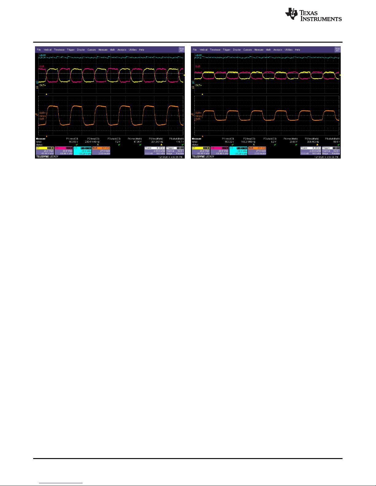
Figure 11 and Figure 12 show this mode at 3 Hz and 1 KHz. Notice that the floating reference (IN-) will
vary based on the IN+ signal. This drift can be minimized by increasing the frequency. This configuration
should only be used as long as the application can handle this drift. Each application should be properly
evaluated to verify if this configuration will be acceptable per its system requirements. Figure 11 and
Figure 12 are with the EVM powered through USB (5 V).
See Figure 13 for a diagram of the input configuration.
Figure 10. Set Reference to External 2.5 V
PWM, Analog, and Single-Ended Inputs
, this floating
BST
SLOU403C–March 2015–Revised June 2018
Submit Documentation Feedback
DRV2700EVM High Voltage Piezo Driver Evaluation Kit
Copyright © 2015–2018, Texas Instruments Incorporated
17
Page 18
IN+
INí
R
16
10.0 NŸ
R
16
10.0 NŸ
Filter
Network
Filter
Network
PWM+
PWMí
DC_IN
TP7
TP8
JP13
Signal
Voltage
Not Used in Floating
Reference Config
PWM, Analog, and Single-Ended Inputs
Figure 11. Floating Reference at 3 Hz and No Load Figure 12. Floating Reference at 1 Hz and No Load
www.ti.com
18
DRV2700EVM High Voltage Piezo Driver Evaluation Kit
Figure 13. DC Coupled Input Diagram
Copyright © 2015–2018, Texas Instruments Incorporated
SLOU403C–March 2015–Revised June 2018
Submit Documentation Feedback
Page 19
DRV2700
Piezo
Element
BST
OUT>
OUT+
GND
DRV2700
BST
OUT>
OUT+
GND
100 Vp
Piezo
Element
100 Vp
Piezo
Element
Piezo
Element
100 Vp
100 Vp
DRV2700
Piezo
Element
BST
OUT-
OUT+
GND
200 Vpp
www.ti.com
6 Output
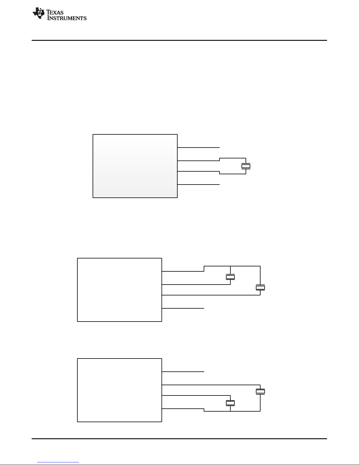
The DRV2700 has 3 main outputs and GND on the 4-terminal output:
1. The output of the boost converter (BST)
2. The positive output of the amplifier (OUT+)
3. The negative output of the amplifier (VOUT–)
These outputs can be configured in a variety of ways and are described in more detail in this section.
6.1 Two Terminal Differential Output Configuration (OUT+ – OUT–)
The typical output configuration is a 2 terminal differential output with one terminal connected to OUT+
and the other connected to OUT–. This configuration can achieve 200 Vpp.
Figure 14. Two Terminal Differential Output
Output
6.2 Two Terminal Single Ended Output Configuration (OUT± to BST/GND)
This output configuration allows for 2 outputs that are 180 degrees out of phase. This is configured with
OUT+ and/or OUT– referenced to GND with a voltage that can swing up to 100 V. Additionally, they can
be referenced to BST.
SLOU403C–March 2015–Revised June 2018
Submit Documentation Feedback
Figure 15. Two Terminal Single Ended Output
Copyright © 2015–2018, Texas Instruments Incorporated
DRV2700EVM High Voltage Piezo Driver Evaluation Kit
19
Page 20
Piezo
Element
DRV2700
Piezo
Element
BST
OUT>
OUT+
GND
100 Vp
100 Vp
Output
6.3 Three Terminal Single Ended Output Configuration (BST to OUT± to GND)
The output configuration is very similar to the two terminal, however, only one output pin is used. This
ensures that the two voltage potentials (BST to OUTx and OUTx to GND) always add up to BST.
Figure 16. Three Terminal Single Ended Output
7 Load Selection
The DRV2700 is intended to drive Piezo (capacitive) loads, however, an improper load driven at certain
levels can cause the device to heat up and hit thermal shutdown. Therefore, there are several key
specifications to consider when choosing a Piezo load; such as dimensions, blocking force, and
displacement. However, the key electrical specifications from the driver perspective are voltage rating and
capacitance. At the maximum frequency of 500 Hz, the DRV2700 is optimized to drive up to 50 nF at 200
VPP, which is the highest voltage swing capability. The DRV2700 will drive larger capacitances if the
programmed boost voltage is lowered or the user limits the input frequency range to lower frequencies (for
example, 300 Hz). For more information, see the Piezo Load Selection section of the DRV2700 data sheet
(SLOS861).
See Figure 13 for a diagram of the input configuration.
www.ti.com
20
DRV2700EVM High Voltage Piezo Driver Evaluation Kit
Copyright © 2015–2018, Texas Instruments Incorporated
SLOU403C–March 2015–Revised June 2018
Submit Documentation Feedback
Page 21

www.ti.com
8 Filtering and Adapting PWM Waveforms
The DRV2700EVM has the capability to support many different input filter configurations. Depending on
the input mode, input frequency, and input voltage, the filter can be adapted to attenuate any undesired
out-of-band content. This section describes the input filter requirements and the various respective
configurations.
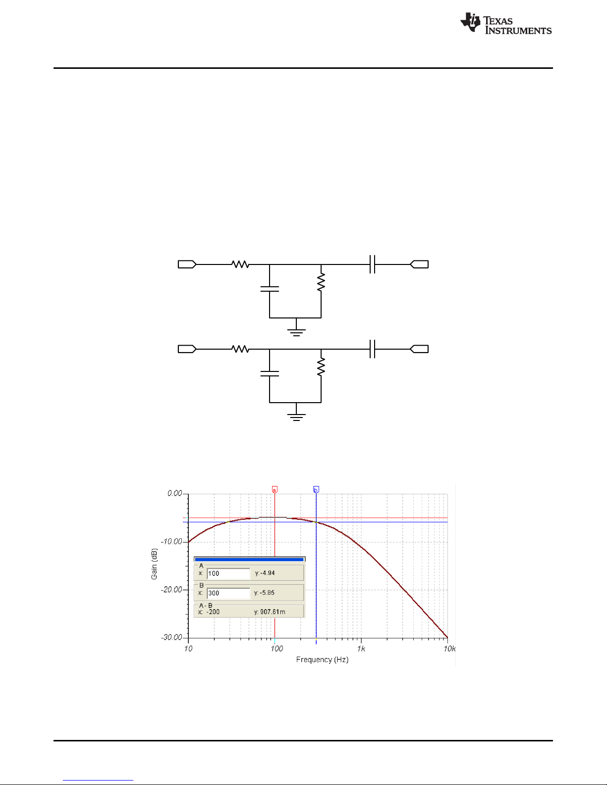
8.1 PWM Input
When using a high-frequency PWM input, a low-pass filter is required. The primary parameters for
determining the input filter are the PWM input frequency and sample rate. Because of the power ratings of
the DRV2700, the input filter has been designed to attenuate frequencies above 500 Hz. For samples
rates above 20 kHz, a simple first-order RC filter is recommended; however, for sample rates much lower
(such as 8 kHz), a first-order filter may not sufficiently attenuate the high-frequency content. Thus, for
lower sampling rates, a second order RC filter may be required. The following sections describe example
filter configurations for both first- and second-order filters. The DRV2700EVM default configuration uses a
second-order differential filter, but it can be replaced by a first-order, single-ended, or differential filter.
Filtering and Adapting PWM Waveforms
Figure 17. DRV2700EVM First- and Second-Order Filters
SLOU403C–March 2015–Revised June 2018
Submit Documentation Feedback
DRV2700EVM High Voltage Piezo Driver Evaluation Kit
Copyright © 2015–2018, Texas Instruments Incorporated
21
Page 22
R
17
7.5k
R
13
4.99k
C
15
100n
C
16
100n
IN+
R
18
7.5k
R
14
4.99k
C
18
100n
C
19
100n
INí
Filtering and Adapting PWM Waveforms
8.2 Filter Selection Criteria
Apply these criteria to select an input filter:
1. First-order RC filters, both single-ended and differential, are recommended for 20 kHz and higher data
sample rates. The first-order filters have adequate settling time and the fewest components.
2. Second-order filters are recommended for noiseless operation when using a lower data sample rate
where a sharper cutoff is necessary
3. The attenuation at the PWM carrier frequency should be at least –40 dB
8.2.1 First-Order Filter
For sample rates 20 kHz and greater, a first-order filter is recommended. The first-order filter is used in
both single-ended or differential configurations. Figure 18 shows a differential, first-order filter. The PWM
input filter is optimized for a 3.3-V differential PWM input signal (–11-dB attenuation); remove R17 and
R18 when applying a 1.8-V input signal.
www.ti.com
Figure 18. Differential, First-Order Filter
The first-order filter in Figure 18 contains one pole with a slope of –20 dB. Figure 19 shows the frequency
response of the first-order filter.
Figure 19. Frequency Response of the First-Order Filter
22
DRV2700EVM High Voltage Piezo Driver Evaluation Kit
Copyright © 2015–2018, Texas Instruments Incorporated
SLOU403C–March 2015–Revised June 2018
Submit Documentation Feedback
Page 23

R
17
2.7k
R
13
3.3k
C
15
47n
C
16
100n
IN+
R
18
2.7k
R
14
3.3k
C
18
47n
C
19
100n
INí
R
6
3.3k
C
15
47n
R
7
3.3k
C
18
47n
www.ti.com
8.2.2 Second-Order Filter, Differential
For data sample rates less than 20 kHz, a second-order filter is recommended. A differential input signal is
recommended for use with a second-order filter because of the longer settling time. Figure 20 shows the
differential, second-order filter that is the default filter configuration for the EVM. The PWM input filter is
optimized for a 3.3-V differential PWM input signal (–1-dB attenuation); remove R17 and R18 when
applying a 1.8-V input signal.
Filtering and Adapting PWM Waveforms
Figure 20. Differential, Second-Order Filter
The second-order filter in Figure 20 contains two poles resulting in a slope of –40 dB. Figure 21 shows the
frequency response of the second-order filter.
Figure 21. Frequency Response of the Second-Order Filter
SLOU403C–March 2015–Revised June 2018
Submit Documentation Feedback
DRV2700EVM High Voltage Piezo Driver Evaluation Kit
Copyright © 2015–2018, Texas Instruments Incorporated
23
Page 24

Filtering and Adapting PWM Waveforms
8.2.3 Remove Filter for Analog Input
If the input signal is an analog waveform, as opposed to a PWM, then an input filter may not be
necessary. Before removing the filter, ensure that a simple RC filter is not needed to remove any artifacts
from the digital-to-analog converter (DAC) output or other input source. Follow these instructions to
remove the input filter completely.
1. Replace resistors R6, R7, R13, and R14 with 0-Ω resistors
2. Remove resistors R17 and R18
3. Remove capacitors C8, C9, C13, and C14. Do not remove ac coupling capacitors C4 and C5.
See Figure 13 for a diagram of the input configuration.
www.ti.com
24
DRV2700EVM High Voltage Piezo Driver Evaluation Kit
Copyright © 2015–2018, Texas Instruments Incorporated
SLOU403C–March 2015–Revised June 2018
Submit Documentation Feedback
Page 25
IN
1
2
EN3NC
4
OUT
5
GND
U3
TLV70033DCKR
1000pF
C2
0.047µF
C14
0.047µF
C17
0.047µF
C15
0.047µF
C18
PWM-
GAIN1
GAIN0
EN
0.1µF
C13
BST
0.1µF
C16
0.1µF
C19
3.3k
R6
3.3k
R7
3.3k
R13
3.3k
R14
2.7k
R17
2.7k
R18
21
SW2
0.1µF
C7
10k
R20
JP3
P6.0/CB0/A0
1
P6.1/CB1/A1
2
P6.2/CB2/A2
3
P6.3/CB3/A3
4
P5.0/A8/VEREF+
5
P5.1/A9/VEREF-
6
AVCC1
7
P5.4/XIN
8
P5.5/XOUT
9
AVSS1
10
DVCC1
11
DVSS1
12
VCORE
13
P1.0/TA0CLK/ACLK
14
P1.1/TA0.0
15
P1.2/TA0.1
16
P1.3/TA0.2
17
P1.4/TA0.3
18
P1.5/TA0.4
19
P1.6/TA1CLK/CBOUT
20
P1.7/TA1.0
21
P2.0/TA1.1
22
PJ.0/TDO
23
PJ.1/TDI/TCLK
24
PJ.2/TMS
25
PJ.3/TCK
26
DVSS2
27
DVCC2
28
P4.0/PM_UCB1STE/PM_UCA1CLK
29
P4.1/PM_UCB1SIMO/PM_UCB1SDA
30
P4.2/PM_UCB1SOMI/PM_UCB1SCL
31
P4.3/PM_UCB1CLK/PM_UCA1STE
32
P4.4/PM_UCA1TXD/PM_UCA1SIMO
33
P4.5/PM_UCA1RXD/PM_UCA1SOMI
34
P4.6/PM_NONE
35
P4.7/PM_NONE
36
VSSU
37
PU.0/DP
38
PUR
39
PU.1/DM
40
VBUS
41
VUSB
42
V18
43
AVSS2
44
P5.2/XT2IN
45
P5.3/XT2OUT
46
TEST/SBWTCK
47
RST/NMI/SBWTDIO
48
PAD
U4
MSP430F5510IRGZ
SCL
SDA
VBUS
1
D-
2
D+
3
ID
4
GND
5
678
9
J1
10µF
C4
100µF
C3
J2
10µF
C1
VBUS
0.1µF
C11
VBUS
D+
D-
0.47µF
C9
1
2
3
4
5
6
J4
9.76k
R10
49.9k
R1
49.9kR323.2k
R2
80.6k
R4
806k
R5
JP2JP4
TRIG
PWM+
Green
1
2
D3
511
R30
VIN
IN-
3p3
3p3
3p3
3p3
GND
GND
GND
GND
GND
GND
GND
GND GND
0.1µF
C12
GND
GND
GND
GND
GND
BST
JP12
PVDD
0.1µF
C5
GND
3.3k
R22
3.3k
R23
Green
1
2
D4
511
R25
Green
1
2
D5
511
R26
Green
1
2
D6
511
R27
EN GAIN1 GAIN0
3.3k
R24
GNDGNDGND
1
2
J5
1
2
3
JP9
1
2
3
JP8
1
2
3
JP7
1
2
3
JP10
VIN
1
2
3
JP11
VIN
VBUS
1
2
3
J3
GND
TP6
0.1uF
C6
IO1
1
IO2
2
GND3IO3
4
IO4
5
VCC
6
U2
TPD4E004DRY
VBUS
GND
GND
VBUS
VDRV
VREST
VREST VREST VREST
TP5
IN+
10.0k
R16
10.0k
R19
GND
DC_IN
JP5
SBWTDIO
SBWTCK
TP4
TP7
TP8
JP13
IN+
GND
100
R15
1.0Meg
R12
VBUS
GND
PUR
2
1
SW1
33
R9
33
R8
D+
D-
1.40k
R11
D+
PUR
0.22µF
C8
0.22µF
C10
1
3 4
2
G
G
12MHz
Y1
ABM8G-12.000MHZ-B4Y-T
JP6
10k
R28
10k
R29
3p3
SCL
SDA
TEST2
TEST1
TEST3
TP1
DNP
TP2
DNP
TP3
DNP
10pF
C23
10pF
C22
5.6V
D1 5.6V
D2
DNP
DNP
GND
GND
GND
GND
GND
VPUMP
1
VDD
2
FB
3
GND
4
GND
5
GND
6
SW
7
SW
8
NC
9
BST
10
BST
11
PVDD
12
OUT+
13
OUT-
14
REXT
15
IN-
16
IN+
17
GAIN0
18
GAIN1
19
EN
20
PAD
21
U1
DRV2700RGP
0.1µF
C21
FB
OUT+
OUT-
1
2
3
4
J6
GND
GND
BST
6.04k
R21
4.7µH2.7A
L1
VDRV
GND
GND
VDRV
GND
0.1µF
C20
FB
IN+
IN-
PWM+_MSP PWM-_MSP
EN_MSP
GAIN1_MSP
GAIN0_MSP
EN_MSP GAIN1_MSP GAIN0_MSP
PWM+_MSP
PWM-_MSP
Power Inputs
Power Routing
DRV2700 Input Routing
DRV2700
MSP430
Boost Voltage Selection
Gain & E N Settings
External I2C
www.ti.com
Reference
25
SLOU403C–March 2015– Revised June 2018
Submit Documentation Feedback
Copyright © 2015–2018, Texas Instruments Incorporated
DRV2700EVM High Voltage Piezo Driver Evaluation Kit
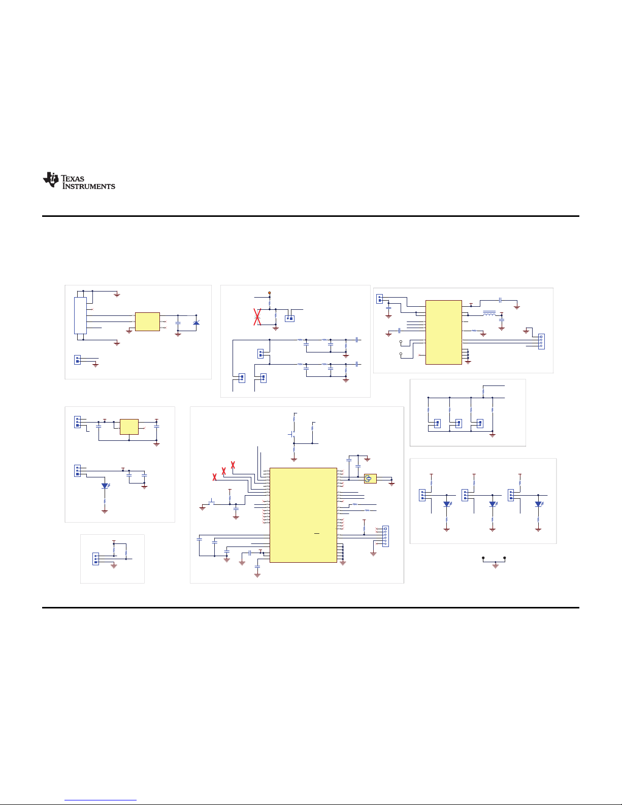
9 Reference
This section includes the DRV2700EVM schematic, PCB Layout, and Bill of Materials.
9.1 Schematic
Figure 22 illustrates the DRV2700EVM schematic.
Figure 22. DRV2700EVM Schematic
Page 26
Reference
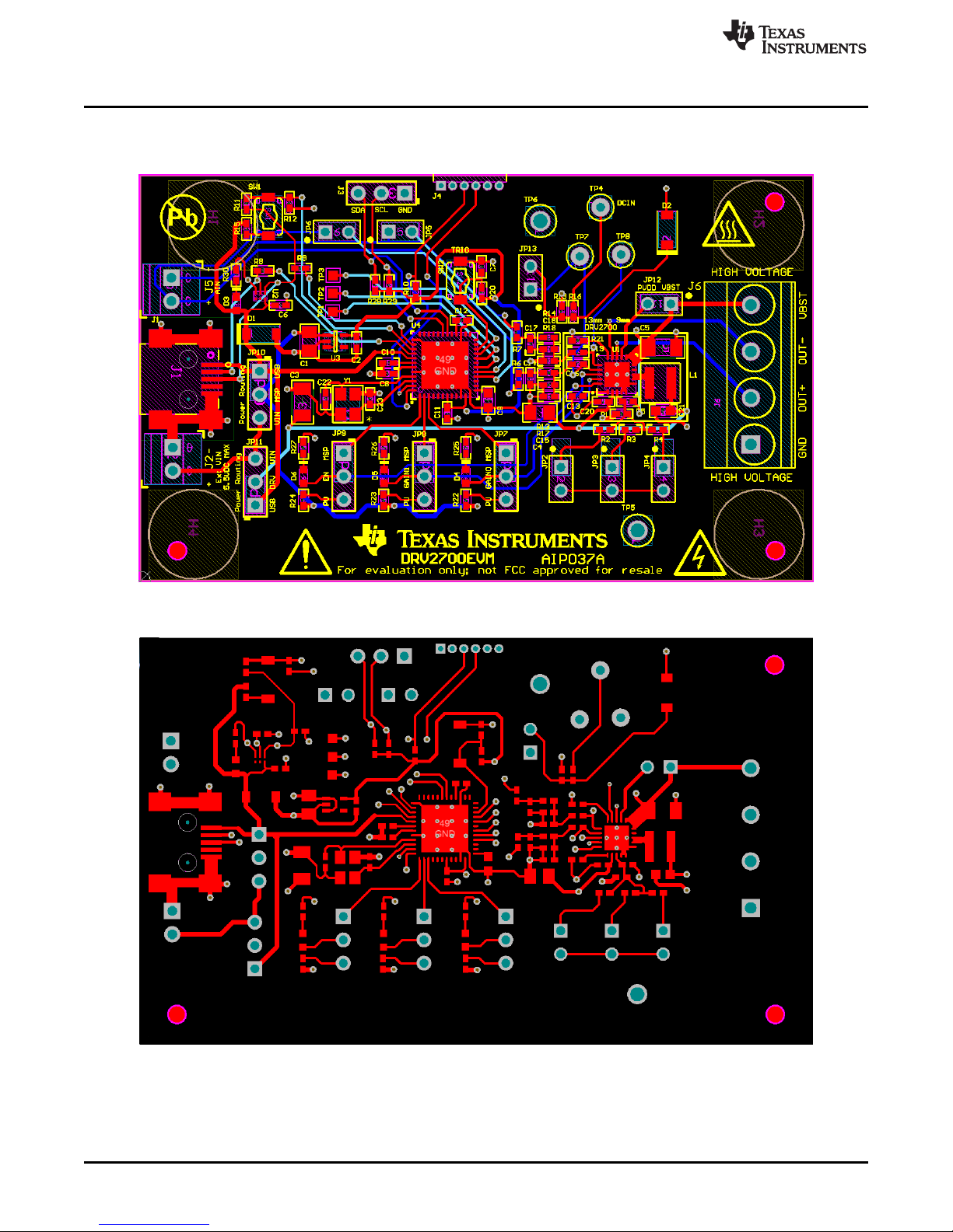
9.2 PCB Layout
Figure 23 through Figure 27 show the DRV2700EVM PCB layouts.
www.ti.com
Figure 23. All Layers
26
DRV2700EVM High Voltage Piezo Driver Evaluation Kit
Figure 24. Top Layer
Copyright © 2015–2018, Texas Instruments Incorporated
SLOU403C–March 2015–Revised June 2018
Submit Documentation Feedback
Page 27
www.ti.com
Reference
Figure 25. Mid Layer 1
SLOU403C–March 2015–Revised June 2018
Submit Documentation Feedback
Figure 26. Mid Layer 2
DRV2700EVM High Voltage Piezo Driver Evaluation Kit
Copyright © 2015–2018, Texas Instruments Incorporated
27
Page 28

Reference
www.ti.com
Figure 27. Bottom Layer
9.3 Bill of Materials
Table 6 lists the DRV2700EVM bill of materials.
Table 6. Bill of Materials
Designator Qty. Value Description Package Reference Part Number Manufacturer
PCB 1 Printed Circuit Board AIP037 Any
C1, C4 2 10µF CAP, CERM, 10uF, 16V, ±20%, X5R, 0805 805 0805YD106MAT2A AVX
C2 1 1000pF CAP, CERM, 1000pF, 6.3V, ±10%, X5R, 0402 402 GRM155R60J102KA01D Murata
C3 1 100 µF CAP, CERM, 100uF, 6.3V, ±20%, X5R, 1206 1206 GRM31CR60J107ME39L Murata
C5 1 0.1 µF CAP, CERM, 0.1uF, 250V, ±10%, X7R, 1206 1206 C3216X7R2E104K TDK
C6 1 0.1 µF CAP CER 0.1UF 16V 5% X7R 0402 402 GRM155R71C104JA88D
C7, C11, C12 3 0.1µF CAP, CERM, 0.1uF, 6.3V, ±10%, X5R, 0402 402 C1005X5R0J104K TDK
C8, C10 2 0.22 µF CAP, CERM, 0.22uF, 6.3V, ±10%, X6S, 0402 402 GRM155C80J224KE01D Murata
C9 1 0.47 µF CAP, CERM, 0.47uF, 10V, ±10%, X7R, 0603 603 C0603C474K8RACTU Kemet
C13, C16, C19, C20 4 0.1 µF CAP, CERM, 0.1uF, 16V, ±10%, X7R, 0402 402 GRM155R71C104KA88D Murata
C14, C15, C17, C18 4 0.047 µF CAP, CERM, 0.047uF, 16V, ±10%, X7R, 0402 402 GRM155R71C473KA01D Murata
C21 1 0.1 µF CAP, CERM, 0.1uF, 25V, ±10%, X5R, 0603 603 06033D104KAT2A AVX
C22, C23 2 10 pF CAP, CERM, 10pF, 50V, ±5%, C0G/NP0, 0402 402 GRM1555C1H100JA01D Murata
D1 1 5.6 V Diode, Zener, 5.6V, 500 mW, SOD-123 SOD-123 MMSZ5232B-7-F Diodes Inc.
D3, D4, D5, D6 4 Green LED, Green, SMD 1.6x0.8x0.8mm LTST-C190KGKT Lite-On
H1, H2, H3, H4 4 Bumpon, Hemisphere, 0.375 × 0.235, Black Black Bumpon SJ61A2 3M
J1 1 Connector, USB Mini B Connector, Mini B 897-43-005-00-100001 Mill-Max
J2, J5 2 Header, 2 Pos, 6A, 63V, TH 6.2x8.5x5.54 mm 1725656 Phoenix Contact
J3, JP7–JP10, JP11 6 Header, 100mil, 3x1, Tin, TH Header, 3x1,100mil,TH 5-146278-3 TE Connectivity
J4 1 Receptacle, 50mil, 6x1, R/A, TH 6x1 Receptacle LPPB061NGCN-RC
J6 1 Terminal Block, 4x1, 5.08 mm, TH 4x1 Terminal Block 39544-3004 Molex
JP2–JP6, JP12, JP13 7 Header, 100mil, 2x1, Tin, TH Header,2 Pin,100mil,Tin PEC02SAAN
Murata Electronics
North America
Sullins Connector
Solutions
Sullins Connector
Solutions
28
DRV2700EVM High Voltage Piezo Driver Evaluation Kit
Copyright © 2015–2018, Texas Instruments Incorporated
SLOU403C–March 2015–Revised June 2018
Submit Documentation Feedback
Page 29

www.ti.com
Reference
Table 6. Bill of Materials (continued)
Designator Qty. Value Description Package Reference Part Number Manufacturer
L1 1 4.7 µH
R1, R3 2 49.9 k RES, 49.9 kΩ, 1%, 0.063W, 0402 402 CRCW040249K9FKED Vishay-Dale
R2 1 23.2 k RES, 23.2 kΩ, 1%, 0.063W, 0402 402 CRCW040223K2FKED Vishay-Dale
R4 1 80.6 k RES, 80.6 kΩ, 1%, 0.063W, 0402 402 CRCW040280K6FKED Vishay-Dale
R5 1 806 k RES, 806 kΩ, 1%, 0.063W, 0402 402 CRCW0402806KFKED Vishay-Dale
R6, R7, R13, R14,
R22–R24
R8, R9 2 33 RES, 33 Ω, 5%, 0.063W, 0402 402 CRCW040233R0JNED Vishay-Dale
R10 1 9.76 k RES, 9.76 kΩ, 1%, 0.063W, 0402 402 CRCW04029K76FKED Vishay-Dale
R11 1 1.40 k RES, 1.40 kΩ, 1%, 0.063W, 0402 402 CRCW04021K40FKED Vishay-Dale
R12 1 1.0 Meg RES, 1.0 MΩ, 5%, 0.063W, 0402 402 CRCW04021M00JNED Vishay-Dale
R15 1 100 RES, 100 Ω, 1%, 0.063W, 0402 402 CRCW0402100RFKED Vishay-Dale
R16, R19 2 10.0 k RES, 10.0 kΩ, 1%, 0.063W, 0402 402 CRCW040210K0FKED Vishay-Dale
R17, R18 2 2.7 k RES, 2.7 kΩ, 5%, 0.063W, 0402 402 CRCW04022K70JNED Vishay-Dale
R20, R28, R29 3 10 k RES, 10 kΩ, 5%, 0.063W, 0402 402 CRCW040210K0JNED Vishay-Dale
R21 1 6.04 k RES, 6.04 kΩ, 1%, 0.063W, 0402 402 CRCW04026K04FKED Vishay-Dale
R25, R26, R27, R30 4 511 RES, 511 Ω, 1%, 0.063W, 0402 402 CRCW0402511RFKED Vishay-Dale
SH-JP1–SH-JP11 11 1x2 Shunt, 2mm, Gold plated, Black 2mm Shunt,Closed Top 2SN-BK-G Samtec
SW1, SW2 2 Switch, Tactile, SPST-NO, 0.05A, 12V, SMT Switch, 4.4x2x2.9 mm TL1015AF160QG E-Switch
TP4 1 Orange Test Point, Miniature, Orange, TH
TP5, TP6 2 Black Test Point, Multipurpose, Black, TH
TP7, TP8 2 White Test Point, Miniature, White, TH White Miniature Testpoint 5002 Keystone
U1 1 Piezo Driver with Integrated Boost Converter, RGP0020D RGP0020D DRV2700RGP Texas Instruments
U2 1
U3 1
U4 1 Mixed Signal MicroController, RGZ0048A RGZ0048A MSP430F5510IRGZ Texas Instruments
Y1 1 CRYSTAL 12.000 MHz 10PF SMD 3.2x0.55x2.5mm
7 3.3 k RES, 3.3 kΩ, 5%, 0.063W, 0402 402 CRCW04023K30JNED Vishay-Dale
Inductor, Shielded, Composite, 4.7 µH,
2.7A, 0.05 Ω, SMD
4-ChanneL ESD-protection array for high-speed data
interfaces, DRY006A
Single Output LDO, 200 mA, Fixed 3.3 V Output, 2 to 5.5
V Input, with Low IQ, 5-pin SC70 (DCK), –40°C to 125°C,
Green (RoHS and no Sb/Br)
4x2x4mm XFL4020-472MEB Coilcraft
Orange Miniature
Testpoint
Black Multipurpose
Testpoint
DRY0006A TPD4E004DRY Texas Instruments
DCK0005A TLV70033DCKR Texas Instruments
5003 Keystone
5011 Keystone
ABM8G-12.000MHZB4Y-T
Abracon Corporation
10 Trademarks
Code Composer Studio, LaunchPad are trademarks of Texas Instruments.
All other trademarks are the property of their respective owners.
SLOU403C–March 2015–Revised June 2018
Submit Documentation Feedback
DRV2700EVM High Voltage Piezo Driver Evaluation Kit
Copyright © 2015–2018, Texas Instruments Incorporated
29
Page 30

Revision History
www.ti.com
Revision History
NOTE: Page numbers for previous revisions may differ from page numbers in the current version.
Changes from Original (March 2015) to A Revision ....................................................................................................... Page
• Changed value on R
in BST Network JP2, JP3, and JP4 image................................................................. 13
5
Revision History
Changes from A Revision (April 2015) to B Revision .................................................................................................... Page
• Changed content in JP11 row of the Default Jumper Settings table. .............................................................. 7
• Changed connector lines in Power Path Diagram. ................................................................................... 8
Revision History
Changes from B Revision (April 2015) to C Revision .................................................................................................... Page
• Added: "MSP-JTAG2SBW JTAG to Spy-Bi-Wire adapter" to the advanced configuration list.................................. 1
• Deleted sentence: "The DRV2700EVM kit includes a JTAG-to-SpyBiWire adapter for connecting the JTAG interface to the
DRV2700EVM SpyBiWire connector" from Section 5.1 ............................................................................ 15
30
Revision History
Copyright © 2015–2018, Texas Instruments Incorporated
SLOU403C–March 2015–Revised June 2018
Submit Documentation Feedback
Page 31

STANDARD TERMS FOR EVALUATION MODULES
1. Delivery: TI delivers TI evaluation boards, kits, or modules, including any accompanying demonstration software, components, and/or
documentation which may be provided together or separately (collectively, an “EVM” or “EVMs”) to the User (“User”) in accordance
with the terms set forth herein. User's acceptance of the EVM is expressly subject to the following terms.
1.1 EVMs are intended solely for product or software developers for use in a research and development setting to facilitate feasibility
evaluation, experimentation, or scientific analysis of TI semiconductors products. EVMs have no direct function and are not
finished products. EVMs shall not be directly or indirectly assembled as a part or subassembly in any finished product. For
clarification, any software or software tools provided with the EVM (“Software”) shall not be subject to the terms and conditions
set forth herein but rather shall be subject to the applicable terms that accompany such Software
1.2 EVMs are not intended for consumer or household use. EVMs may not be sold, sublicensed, leased, rented, loaned, assigned,
or otherwise distributed for commercial purposes by Users, in whole or in part, or used in any finished product or production
system.
2 Limited Warranty and Related Remedies/Disclaimers:
2.1 These terms do not apply to Software. The warranty, if any, for Software is covered in the applicable Software License
Agreement.
2.2 TI warrants that the TI EVM will conform to TI's published specifications for ninety (90) days after the date TI delivers such EVM
to User. Notwithstanding the foregoing, TI shall not be liable for a nonconforming EVM if (a) the nonconformity was caused by
neglect, misuse or mistreatment by an entity other than TI, including improper installation or testing, or for any EVMs that have
been altered or modified in any way by an entity other than TI, (b) the nonconformity resulted from User's design, specifications
or instructions for such EVMs or improper system design, or (c) User has not paid on time. Testing and other quality control
techniques are used to the extent TI deems necessary. TI does not test all parameters of each EVM.
User's claims against TI under this Section 2 are void if User fails to notify TI of any apparent defects in the EVMs within ten (10)
business days after delivery, or of any hidden defects with ten (10) business days after the defect has been detected.
2.3 TI's sole liability shall be at its option to repair or replace EVMs that fail to conform to the warranty set forth above, or credit
User's account for such EVM. TI's liability under this warranty shall be limited to EVMs that are returned during the warranty
period to the address designated by TI and that are determined by TI not to conform to such warranty. If TI elects to repair or
replace such EVM, TI shall have a reasonable time to repair such EVM or provide replacements. Repaired EVMs shall be
warranted for the remainder of the original warranty period. Replaced EVMs shall be warranted for a new full ninety (90) day
warranty period.
3 Regulatory Notices:
3.1 United States
3.1.1 Notice applicable to EVMs not FCC-Approved:
FCC NOTICE: This kit is designed to allow product developers to evaluate electronic components, circuitry, or software
associated with the kit to determine whether to incorporate such items in a finished product and software developers to write
software applications for use with the end product. This kit is not a finished product and when assembled may not be resold or
otherwise marketed unless all required FCC equipment authorizations are first obtained. Operation is subject to the condition
that this product not cause harmful interference to licensed radio stations and that this product accept harmful interference.
Unless the assembled kit is designed to operate under part 15, part 18 or part 95 of this chapter, the operator of the kit must
operate under the authority of an FCC license holder or must secure an experimental authorization under part 5 of this chapter.
3.1.2 For EVMs annotated as FCC – FEDERAL COMMUNICATIONS COMMISSION Part 15 Compliant:
CAUTION
This device complies with part 15 of the FCC Rules. Operation is subject to the following two conditions: (1) This device may not
cause harmful interference, and (2) this device must accept any interference received, including interference that may cause
undesired operation.
Changes or modifications not expressly approved by the party responsible for compliance could void the user's authority to
operate the equipment.
FCC Interference Statement for Class A EVM devices
NOTE: This equipment has been tested and found to comply with the limits for a Class A digital device, pursuant to part 15 of
the FCC Rules. These limits are designed to provide reasonable protection against harmful interference when the equipment is
operated in a commercial environment. This equipment generates, uses, and can radiate radio frequency energy and, if not
installed and used in accordance with the instruction manual, may cause harmful interference to radio communications.
Operation of this equipment in a residential area is likely to cause harmful interference in which case the user will be required to
correct the interference at his own expense.
Page 32

FCC Interference Statement for Class B EVM devices
NOTE: This equipment has been tested and found to comply with the limits for a Class B digital device, pursuant to part 15 of
the FCC Rules. These limits are designed to provide reasonable protection against harmful interference in a residential
installation. This equipment generates, uses and can radiate radio frequency energy and, if not installed and used in accordance
with the instructions, may cause harmful interference to radio communications. However, there is no guarantee that interference
will not occur in a particular installation. If this equipment does cause harmful interference to radio or television reception, which
can be determined by turning the equipment off and on, the user is encouraged to try to correct the interference by one or more
of the following measures:
• Reorient or relocate the receiving antenna.
• Increase the separation between the equipment and receiver.
• Connect the equipment into an outlet on a circuit different from that to which the receiver is connected.
• Consult the dealer or an experienced radio/TV technician for help.
3.2 Canada
3.2.1 For EVMs issued with an Industry Canada Certificate of Conformance to RSS-210 or RSS-247
Concerning EVMs Including Radio Transmitters:
This device complies with Industry Canada license-exempt RSSs. Operation is subject to the following two conditions:
(1) this device may not cause interference, and (2) this device must accept any interference, including interference that may
cause undesired operation of the device.
Concernant les EVMs avec appareils radio:
Le présent appareil est conforme aux CNR d'Industrie Canada applicables aux appareils radio exempts de licence. L'exploitation
est autorisée aux deux conditions suivantes: (1) l'appareil ne doit pas produire de brouillage, et (2) l'utilisateur de l'appareil doit
accepter tout brouillage radioélectrique subi, même si le brouillage est susceptible d'en compromettre le fonctionnement.
Concerning EVMs Including Detachable Antennas:
Under Industry Canada regulations, this radio transmitter may only operate using an antenna of a type and maximum (or lesser)
gain approved for the transmitter by Industry Canada. To reduce potential radio interference to other users, the antenna type
and its gain should be so chosen that the equivalent isotropically radiated power (e.i.r.p.) is not more than that necessary for
successful communication. This radio transmitter has been approved by Industry Canada to operate with the antenna types
listed in the user guide with the maximum permissible gain and required antenna impedance for each antenna type indicated.
Antenna types not included in this list, having a gain greater than the maximum gain indicated for that type, are strictly prohibited
for use with this device.
Concernant les EVMs avec antennes détachables
Conformément à la réglementation d'Industrie Canada, le présent émetteur radio peut fonctionner avec une antenne d'un type et
d'un gain maximal (ou inférieur) approuvé pour l'émetteur par Industrie Canada. Dans le but de réduire les risques de brouillage
radioélectrique à l'intention des autres utilisateurs, il faut choisir le type d'antenne et son gain de sorte que la puissance isotrope
rayonnée équivalente (p.i.r.e.) ne dépasse pas l'intensité nécessaire à l'établissement d'une communication satisfaisante. Le
présent émetteur radio a été approuvé par Industrie Canada pour fonctionner avec les types d'antenne énumérés dans le
manuel d’usage et ayant un gain admissible maximal et l'impédance requise pour chaque type d'antenne. Les types d'antenne
non inclus dans cette liste, ou dont le gain est supérieur au gain maximal indiqué, sont strictement interdits pour l'exploitation de
l'émetteur
3.3 Japan
3.3.1 Notice for EVMs delivered in Japan: Please see http://www.tij.co.jp/lsds/ti_ja/general/eStore/notice_01.page 日本国内に
輸入される評価用キット、ボードについては、次のところをご覧ください。
http://www.tij.co.jp/lsds/ti_ja/general/eStore/notice_01.page
3.3.2 Notice for Users of EVMs Considered “Radio Frequency Products” in Japan: EVMs entering Japan may not be certified
by TI as conforming to Technical Regulations of Radio Law of Japan.
If User uses EVMs in Japan, not certified to Technical Regulations of Radio Law of Japan, User is required to follow the
instructions set forth by Radio Law of Japan, which includes, but is not limited to, the instructions below with respect to EVMs
(which for the avoidance of doubt are stated strictly for convenience and should be verified by User):
1. Use EVMs in a shielded room or any other test facility as defined in the notification #173 issued by Ministry of Internal
Affairs and Communications on March 28, 2006, based on Sub-section 1.1 of Article 6 of the Ministry’s Rule for
Enforcement of Radio Law of Japan,
2. Use EVMs only after User obtains the license of Test Radio Station as provided in Radio Law of Japan with respect to
EVMs, or
3. Use of EVMs only after User obtains the Technical Regulations Conformity Certification as provided in Radio Law of Japan
with respect to EVMs. Also, do not transfer EVMs, unless User gives the same notice above to the transferee. Please note
that if User does not follow the instructions above, User will be subject to penalties of Radio Law of Japan.
Page 33

【無線電波を送信する製品の開発キットをお使いになる際の注意事項】 開発キットの中には技術基準適合証明を受けて
いないものがあります。 技術適合証明を受けていないもののご使用に際しては、電波法遵守のため、以下のいずれかの
措置を取っていただく必要がありますのでご注意ください。
1. 電波法施行規則第6条第1項第1号に基づく平成18年3月28日総務省告示第173号で定められた電波暗室等の試験設備でご使用
いただく。
2. 実験局の免許を取得後ご使用いただく。
3. 技術基準適合証明を取得後ご使用いただく。
なお、本製品は、上記の「ご使用にあたっての注意」を譲渡先、移転先に通知しない限り、譲渡、移転できないものとします。
上記を遵守頂けない場合は、電波法の罰則が適用される可能性があることをご留意ください。 日本テキサス・イ
ンスツルメンツ株式会社
東京都新宿区西新宿6丁目24番1号
西新宿三井ビル
3.3.3 Notice for EVMs for Power Line Communication: Please see http://www.tij.co.jp/lsds/ti_ja/general/eStore/notice_02.page
電力線搬送波通信についての開発キットをお使いになる際の注意事項については、次のところをご覧ください。http:/
/www.tij.co.jp/lsds/ti_ja/general/eStore/notice_02.page
3.4 European Union
3.4.1 For EVMs subject to EU Directive 2014/30/EU (Electromagnetic Compatibility Directive):
This is a class A product intended for use in environments other than domestic environments that are connected to a
low-voltage power-supply network that supplies buildings used for domestic purposes. In a domestic environment this
product may cause radio interference in which case the user may be required to take adequate measures.
4 EVM Use Restrictions and Warnings:
4.1 EVMS ARE NOT FOR USE IN FUNCTIONAL SAFETY AND/OR SAFETY CRITICAL EVALUATIONS, INCLUDING BUT NOT
LIMITED TO EVALUATIONS OF LIFE SUPPORT APPLICATIONS.
4.2 User must read and apply the user guide and other available documentation provided by TI regarding the EVM prior to handling
or using the EVM, including without limitation any warning or restriction notices. The notices contain important safety information
related to, for example, temperatures and voltages.
4.3 Safety-Related Warnings and Restrictions:
4.3.1 User shall operate the EVM within TI’s recommended specifications and environmental considerations stated in the user
guide, other available documentation provided by TI, and any other applicable requirements and employ reasonable and
customary safeguards. Exceeding the specified performance ratings and specifications (including but not limited to input
and output voltage, current, power, and environmental ranges) for the EVM may cause personal injury or death, or
property damage. If there are questions concerning performance ratings and specifications, User should contact a TI
field representative prior to connecting interface electronics including input power and intended loads. Any loads applied
outside of the specified output range may also result in unintended and/or inaccurate operation and/or possible
permanent damage to the EVM and/or interface electronics. Please consult the EVM user guide prior to connecting any
load to the EVM output. If there is uncertainty as to the load specification, please contact a TI field representative.
During normal operation, even with the inputs and outputs kept within the specified allowable ranges, some circuit
components may have elevated case temperatures. These components include but are not limited to linear regulators,
switching transistors, pass transistors, current sense resistors, and heat sinks, which can be identified using the
information in the associated documentation. When working with the EVM, please be aware that the EVM may become
very warm.
4.3.2 EVMs are intended solely for use by technically qualified, professional electronics experts who are familiar with the
dangers and application risks associated with handling electrical mechanical components, systems, and subsystems.
User assumes all responsibility and liability for proper and safe handling and use of the EVM by User or its employees,
affiliates, contractors or designees. User assumes all responsibility and liability to ensure that any interfaces (electronic
and/or mechanical) between the EVM and any human body are designed with suitable isolation and means to safely
limit accessible leakage currents to minimize the risk of electrical shock hazard. User assumes all responsibility and
liability for any improper or unsafe handling or use of the EVM by User or its employees, affiliates, contractors or
designees.
4.4 User assumes all responsibility and liability to determine whether the EVM is subject to any applicable international, federal,
state, or local laws and regulations related to User’s handling and use of the EVM and, if applicable, User assumes all
responsibility and liability for compliance in all respects with such laws and regulations. User assumes all responsibility and
liability for proper disposal and recycling of the EVM consistent with all applicable international, federal, state, and local
requirements.
5. Accuracy of Information: To the extent TI provides information on the availability and function of EVMs, TI attempts to be as accurate
as possible. However, TI does not warrant the accuracy of EVM descriptions, EVM availability or other information on its websites as
accurate, complete, reliable, current, or error-free.
Page 34

6. Disclaimers:
6.1 EXCEPT AS SET FORTH ABOVE, EVMS AND ANY MATERIALS PROVIDED WITH THE EVM (INCLUDING, BUT NOT
LIMITED TO, REFERENCE DESIGNS AND THE DESIGN OF THE EVM ITSELF) ARE PROVIDED "AS IS" AND "WITH ALL
FAULTS." TI DISCLAIMS ALL OTHER WARRANTIES, EXPRESS OR IMPLIED, REGARDING SUCH ITEMS, INCLUDING BUT
NOT LIMITED TO ANY EPIDEMIC FAILURE WARRANTY OR IMPLIED WARRANTIES OF MERCHANTABILITY OR FITNESS
FOR A PARTICULAR PURPOSE OR NON-INFRINGEMENT OF ANY THIRD PARTY PATENTS, COPYRIGHTS, TRADE
SECRETS OR OTHER INTELLECTUAL PROPERTY RIGHTS.
6.2 EXCEPT FOR THE LIMITED RIGHT TO USE THE EVM SET FORTH HEREIN, NOTHING IN THESE TERMS SHALL BE
CONSTRUED AS GRANTING OR CONFERRING ANY RIGHTS BY LICENSE, PATENT, OR ANY OTHER INDUSTRIAL OR
INTELLECTUAL PROPERTY RIGHT OF TI, ITS SUPPLIERS/LICENSORS OR ANY OTHER THIRD PARTY, TO USE THE
EVM IN ANY FINISHED END-USER OR READY-TO-USE FINAL PRODUCT, OR FOR ANY INVENTION, DISCOVERY OR
IMPROVEMENT, REGARDLESS OF WHEN MADE, CONCEIVED OR ACQUIRED.
7. USER'S INDEMNITY OBLIGATIONS AND REPRESENTATIONS. USER WILL DEFEND, INDEMNIFY AND HOLD TI, ITS
LICENSORS AND THEIR REPRESENTATIVES HARMLESS FROM AND AGAINST ANY AND ALL CLAIMS, DAMAGES, LOSSES,
EXPENSES, COSTS AND LIABILITIES (COLLECTIVELY, "CLAIMS") ARISING OUT OF OR IN CONNECTION WITH ANY
HANDLING OR USE OF THE EVM THAT IS NOT IN ACCORDANCE WITH THESE TERMS. THIS OBLIGATION SHALL APPLY
WHETHER CLAIMS ARISE UNDER STATUTE, REGULATION, OR THE LAW OF TORT, CONTRACT OR ANY OTHER LEGAL
THEORY, AND EVEN IF THE EVM FAILS TO PERFORM AS DESCRIBED OR EXPECTED.
8. Limitations on Damages and Liability:
8.1 General Limitations. IN NO EVENT SHALL TI BE LIABLE FOR ANY SPECIAL, COLLATERAL, INDIRECT, PUNITIVE,
INCIDENTAL, CONSEQUENTIAL, OR EXEMPLARY DAMAGES IN CONNECTION WITH OR ARISING OUT OF THESE
TERMS OR THE USE OF THE EVMS , REGARDLESS OF WHETHER TI HAS BEEN ADVISED OF THE POSSIBILITY OF
SUCH DAMAGES. EXCLUDED DAMAGES INCLUDE, BUT ARE NOT LIMITED TO, COST OF REMOVAL OR
REINSTALLATION, ANCILLARY COSTS TO THE PROCUREMENT OF SUBSTITUTE GOODS OR SERVICES, RETESTING,
OUTSIDE COMPUTER TIME, LABOR COSTS, LOSS OF GOODWILL, LOSS OF PROFITS, LOSS OF SAVINGS, LOSS OF
USE, LOSS OF DATA, OR BUSINESS INTERRUPTION. NO CLAIM, SUIT OR ACTION SHALL BE BROUGHT AGAINST TI
MORE THAN TWELVE (12) MONTHS AFTER THE EVENT THAT GAVE RISE TO THE CAUSE OF ACTION HAS
OCCURRED.
8.2 Specific Limitations. IN NO EVENT SHALL TI'S AGGREGATE LIABILITY FROM ANY USE OF AN EVM PROVIDED
HEREUNDER, INCLUDING FROM ANY WARRANTY, INDEMITY OR OTHER OBLIGATION ARISING OUT OF OR IN
CONNECTION WITH THESE TERMS, , EXCEED THE TOTAL AMOUNT PAID TO TI BY USER FOR THE PARTICULAR
EVM(S) AT ISSUE DURING THE PRIOR TWELVE (12) MONTHS WITH RESPECT TO WHICH LOSSES OR DAMAGES ARE
CLAIMED. THE EXISTENCE OF MORE THAN ONE CLAIM SHALL NOT ENLARGE OR EXTEND THIS LIMIT.
9. Return Policy. Except as otherwise provided, TI does not offer any refunds, returns, or exchanges. Furthermore, no return of EVM(s)
will be accepted if the package has been opened and no return of the EVM(s) will be accepted if they are damaged or otherwise not in
a resalable condition. If User feels it has been incorrectly charged for the EVM(s) it ordered or that delivery violates the applicable
order, User should contact TI. All refunds will be made in full within thirty (30) working days from the return of the components(s),
excluding any postage or packaging costs.
10. Governing Law: These terms and conditions shall be governed by and interpreted in accordance with the laws of the State of Texas,
without reference to conflict-of-laws principles. User agrees that non-exclusive jurisdiction for any dispute arising out of or relating to
these terms and conditions lies within courts located in the State of Texas and consents to venue in Dallas County, Texas.
Notwithstanding the foregoing, any judgment may be enforced in any United States or foreign court, and TI may seek injunctive relief
in any United States or foreign court.
Mailing Address: Texas Instruments, Post Office Box 655303, Dallas, Texas 75265
Copyright © 2018, Texas Instruments Incorporated
Page 35

IMPORTANT NOTICE FOR TI DESIGN INFORMATION AND RESOURCES
Texas Instruments Incorporated (‘TI”) technical, application or other design advice, services or information, including, but not limited to,
reference designs and materials relating to evaluation modules, (collectively, “TI Resources”) are intended to assist designers who are
developing applications that incorporate TI products; by downloading, accessing or using any particular TI Resource in any way, you
(individually or, if you are acting on behalf of a company, your company) agree to use it solely for this purpose and subject to the terms of
this Notice.
TI’s provision of TI Resources does not expand or otherwise alter TI’s applicable published warranties or warranty disclaimers for TI
products, and no additional obligations or liabilities arise from TI providing such TI Resources. TI reserves the right to make corrections,
enhancements, improvements and other changes to its TI Resources.
You understand and agree that you remain responsible for using your independent analysis, evaluation and judgment in designing your
applications and that you have full and exclusive responsibility to assure the safety of your applications and compliance of your applications
(and of all TI products used in or for your applications) with all applicable regulations, laws and other applicable requirements. You
represent that, with respect to your applications, you have all the necessary expertise to create and implement safeguards that (1)
anticipate dangerous consequences of failures, (2) monitor failures and their consequences, and (3) lessen the likelihood of failures that
might cause harm and take appropriate actions. You agree that prior to using or distributing any applications that include TI products, you
will thoroughly test such applications and the functionality of such TI products as used in such applications. TI has not conducted any
testing other than that specifically described in the published documentation for a particular TI Resource.
You are authorized to use, copy and modify any individual TI Resource only in connection with the development of applications that include
the TI product(s) identified in such TI Resource. NO OTHER LICENSE, EXPRESS OR IMPLIED, BY ESTOPPEL OR OTHERWISE TO
ANY OTHER TI INTELLECTUAL PROPERTY RIGHT, AND NO LICENSE TO ANY TECHNOLOGY OR INTELLECTUAL PROPERTY
RIGHT OF TI OR ANY THIRD PARTY IS GRANTED HEREIN, including but not limited to any patent right, copyright, mask work right, or
other intellectual property right relating to any combination, machine, or process in which TI products or services are used. Information
regarding or referencing third-party products or services does not constitute a license to use such products or services, or a warranty or
endorsement thereof. Use of TI Resources may require a license from a third party under the patents or other intellectual property of the
third party, or a license from TI under the patents or other intellectual property of TI.
TI RESOURCES ARE PROVIDED “AS IS” AND WITH ALL FAULTS. TI DISCLAIMS ALL OTHER WARRANTIES OR
REPRESENTATIONS, EXPRESS OR IMPLIED, REGARDING TI RESOURCES OR USE THEREOF, INCLUDING BUT NOT LIMITED TO
ACCURACY OR COMPLETENESS, TITLE, ANY EPIDEMIC FAILURE WARRANTY AND ANY IMPLIED WARRANTIES OF
MERCHANTABILITY, FITNESS FOR A PARTICULAR PURPOSE, AND NON-INFRINGEMENT OF ANY THIRD PARTY INTELLECTUAL
PROPERTY RIGHTS.
TI SHALL NOT BE LIABLE FOR AND SHALL NOT DEFEND OR INDEMNIFY YOU AGAINST ANY CLAIM, INCLUDING BUT NOT
LIMITED TO ANY INFRINGEMENT CLAIM THAT RELATES TO OR IS BASED ON ANY COMBINATION OF PRODUCTS EVEN IF
DESCRIBED IN TI RESOURCES OR OTHERWISE. IN NO EVENT SHALL TI BE LIABLE FOR ANY ACTUAL, DIRECT, SPECIAL,
COLLATERAL, INDIRECT, PUNITIVE, INCIDENTAL, CONSEQUENTIAL OR EXEMPLARY DAMAGES IN CONNECTION WITH OR
ARISING OUT OF TI RESOURCES OR USE THEREOF, AND REGARDLESS OF WHETHER TI HAS BEEN ADVISED OF THE
POSSIBILITY OF SUCH DAMAGES.
You agree to fully indemnify TI and its representatives against any damages, costs, losses, and/or liabilities arising out of your noncompliance with the terms and provisions of this Notice.
This Notice applies to TI Resources. Additional terms apply to the use and purchase of certain types of materials, TI products and services.
These include; without limitation, TI’s standard terms for semiconductor products http://www.ti.com/sc/docs/stdterms.htm), evaluation
modules, and samples (http://www.ti.com/sc/docs/sampterms.htm).
Mailing Address: Texas Instruments, Post Office Box 655303, Dallas, Texas 75265
Copyright © 2018, Texas Instruments Incorporated
 Loading...