

Page 1
User's Guide
SLOU389A–May 2014–Revised June 2014
DRV2605L ERM and LRA Haptic Driver Evaluation Kit
The DRV2605L is a haptic driver designed for linear resonant actuators (LRA) and eccentric rotating mass
(ERM) motors. It provides many features, which help eliminate the design complexities of haptic motor
control including:
• Reduced solution size
• High-efficiency output drive
• Closed-loop motor control
• Quick device startup
• Embedded waveform library
• Auto-resonance frequency tracking
The DRV2605LEVM-CT evaluation module (EVM) is a complete demo and evaluation platform for the
DRV2605L. The kit includes a microcontroller, linear actuator, eccentric rotating mass motor, sample
waveforms, and capacitive touch buttons, which can completely demonstrate and evaluate the DRV2605L.
This user's guide contains instructions to setup and operate the DRV2605LEVM-CT in demonstration and
evaluation mode.
Evaluation Kit Contents:
• DRV2605LEVM-CT demo and evaluation board
• Mini-USB cable
• Demonstration mode firmware
Needed for programming and advanced configuration:
• Code Composer Studio™ (CCS) or IAR Embedded Workbench IDE for MSP430
• MSP430 LaunchPad (MSP-EXP430G2), or MSP430-FET430UIF hardware programming tool
• DRV2605LEVM-CT firmware available on www.ti.com
SLOU389A–May 2014–Revised June 2014 DRV2605L ERM and LRA Haptic Driver Evaluation Kit
Submit Documentation Feedback
1
Copyright © 2014, Texas Instruments Incorporated
Page 2

www.ti.com
Contents
1 Getting Started............................................................................................................... 4
1.1 Evaluation Module Operating Parameters ...................................................................... 5
1.2 Quick Start Board Setup........................................................................................... 5
2 DRV2605L Demonstration Program....................................................................................... 6
2.1 Demo Mode.......................................................................................................... 7
2.2 Description of the Demo Modes .................................................................................. 8
2.3 ROM Library Mode................................................................................................ 13
2.4 ROM Library Effects List ......................................................................................... 14
3 Additional Hardware Modes............................................................................................... 15
3.1 Enter Binary Counting Mode..................................................................................... 15
3.2 Exit Binary Counting Mode....................................................................................... 15
3.3 Binary Counting Modes........................................................................................... 16
4 Hardware Configuration ................................................................................................... 17
4.1 Input and Output Overview ...................................................................................... 17
4.2 Power Supply Selection .......................................................................................... 17
4.3 Using an External Actuator....................................................................................... 18
4.4 PWM Input ......................................................................................................... 19
4.5 External Trigger Control ......................................................................................... 20
4.6 External I
2
C Input.................................................................................................. 21
4.7 Audio-to-Haptics Input............................................................................................ 22
5 Measurement and Analysis .............................................................................................. 23
6 MSP430 Firmware ......................................................................................................... 24
6.1 MSP430 Pinout.................................................................................................... 25
7 Schematic ................................................................................................................... 26
8 Layout........................................................................................................................ 27
9 Bill of Materials ............................................................................................................. 30
List of Figures
1 Board Diagram............................................................................................................... 4
2 DRV2605LEVM-CT Mode Sets............................................................................................ 6
3 ERM Click and Ramp-Down Waveform (Button 1)...................................................................... 8
4 LRA Ramp-Up and Pulsing Waveform (Button 4)....................................................................... 8
5 ERM SharpClick_100 (Button 1)........................................................................................... 8
6 ERM StrongClick_60 and Release SharpClick_100 (Button 2)........................................................ 8
7 LRA SharpTick2_80 (Button 1) ............................................................................................ 9
8 LRA StrongClick 100 and Release SharpTick2 80 (Button 2) ......................................................... 9
9 LRA Auto-Resonance On (Button 1)...................................................................................... 9
10 LRA Auto-Resonance Off (Button 2)...................................................................................... 9
11 LRA Acceleration versus Frequency over Output Voltage............................................................ 10
12 ERM Closed Loop (Button 3)............................................................................................. 10
13 ERM Open Loop (Button 4)............................................................................................... 10
14 ERM Audio-to-Haptics Conversion (Button 1).......................................................................... 12
15 LRA Audio-to-Haptics Conversion (Button 2)........................................................................... 12
16 Power Jumper Selection .................................................................................................. 18
17 Terminal Block and Test Points .......................................................................................... 18
18 External PWM Input........................................................................................................ 19
19 External Trigger Control................................................................................................... 20
20 External I
2
C Input........................................................................................................... 21
21 Audio-to-Haptics Input..................................................................................................... 22
22 Terminal Block and Test Points .......................................................................................... 23
23 DRV2605L Unfiltered Waveform ......................................................................................... 23
2
DRV2605L ERM and LRA Haptic Driver Evaluation Kit SLOU389A–May 2014–Revised June 2014
Copyright © 2014, Texas Instruments Incorporated
Submit Documentation Feedback
Page 3

www.ti.com
24 DRV2605L Filtered Waveform............................................................................................ 23
25 Measuring the DRV2605L Output Signal With an Analog Low-Pass Filter......................................... 23
26 LaunchPad Programmer Connection.................................................................................... 24
27 DRV2605LEVM-CT Schematic........................................................................................... 26
28 X-Ray Top View ............................................................................................................ 27
29 Top Copper ................................................................................................................. 27
30 Layer 2 Copper............................................................................................................. 28
31 Layer 3 Copper............................................................................................................. 28
32 Bottom Copper.............................................................................................................. 29
1 Jumper Descriptions......................................................................................................... 5
2 Mode and Effects Table..................................................................................................... 7
3 DRV2605L Library Table.................................................................................................. 13
4 Binary Counting Modes.................................................................................................... 16
5 Hardware Overview........................................................................................................ 17
6 MSP430 Pinout............................................................................................................. 25
7 Bill of Materials ............................................................................................................. 30
List of Tables
SLOU389A–May 2014–Revised June 2014 DRV2605L ERM and LRA Haptic Driver Evaluation Kit
Submit Documentation Feedback
3
Copyright © 2014, Texas Instruments Incorporated
Page 4
Actuators
DRV2605L
MSP430
OUT
USB
VBAT
SBW
MSP
DRV
USB Power
External
Power
Power Select Pins
DRV2605L
Increment Mode
Decrement Mode ERM and LRA Actuators
Effect Buttons
Press to play haptic effects.
Programmer
Connector
AUDIO
Audio-to-
Haptics
JP4
JP3
Actuator Disconnect
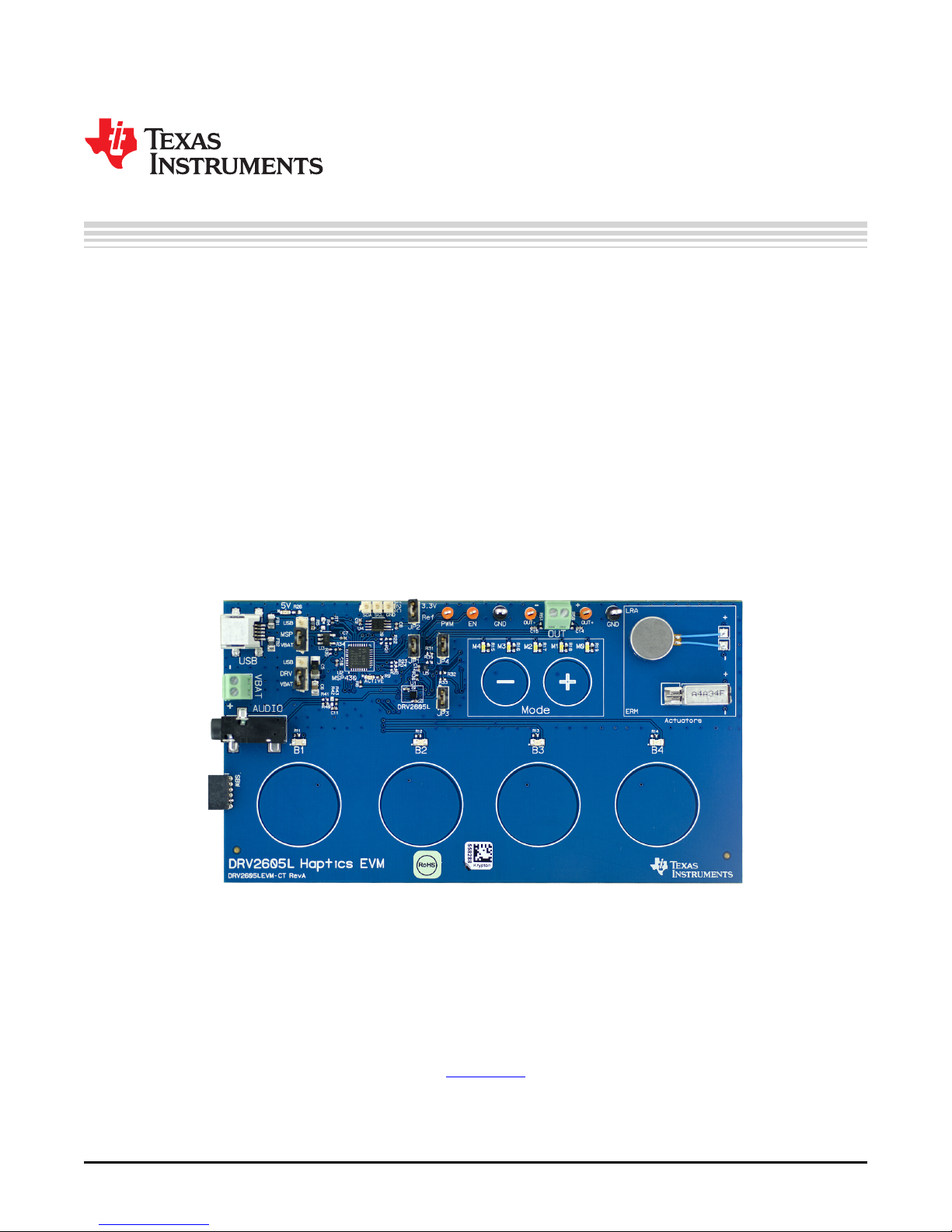
Getting Started
1 Getting Started
The DRV2605L can be used as a demonstration or evaluation tool. When the DRV2605LEVM-CT is
powered on for the first time, a demo application automatically starts. To power the board, connect the
DRV2605LEVM-CT to an available USB port on your computer using the included mini-USB cable. The
demo begins with a board power-up sequence, and then enters the demo effects mode. The four larger
buttons (B1 to B4) can be used to sample haptic effects using both the ERM and LRA motor in the top
right corner. The two smaller mode buttons (“–“ and “+”) are used to change between the different banks
of effects. See the DRV2605L Demonstration Program section for a more detailed description of the demo
application.
www.ti.com
Figure 1. Board Diagram
Code Composer Studio is a trademark of Texas Instruments.
All other trademarks are the property of their respective owners.
4
DRV2605L ERM and LRA Haptic Driver Evaluation Kit SLOU389A–May 2014–Revised June 2014
Copyright © 2014, Texas Instruments Incorporated
Submit Documentation Feedback
Page 5
www.ti.com
1.1 Evaluation Module Operating Parameters
The following table lists the operating conditions for the DRV2605L on the evaluation module.
Parameter Specification
Supply voltage range 2.5 to 5.5 V
Power-supply current rating 400 mA
1.2 Quick Start Board Setup
The DRV2605LEVM-CT firmware contains haptic waveforms which showcase the features and benefits of
the DRV2605L. Follow the instructions below to begin the demo.
1. Out of the box, the jumpers are set to begin demo mode using USB power. The default jumper settings
can be found in Table 1.
Table 1. Jumper Descriptions
Jumper Default Position Description
JP1 Shorted Connect MSP430 GPIO or PWM output to DRV2605L IN/TRIG
JP2 Shorted 3.3-V reference for I2C
JP3, JP4 Shorted Connect on-board actuators to DRV2605L
MSP USB to MSP Select USB (5 V) or VBAT power for the MSP430
DRV USB to DRV Select USB (5 V) or VBAT power for the DRV2605L
Getting Started
2. Connect the included mini-USB cable to the USB connector on the DRV2605LEVM-CT board.
3. Connect the other end of the USB cable to an available USB port on a computer, USB charger, or USB
battery pack.
4. If the board is powered correctly, the four colored LEDs turn on, four mode LEDs flash, and the LRA
and ERM perform auto-calibration, indicating the board has been successfully initialized.
SLOU389A–May 2014–Revised June 2014 DRV2605L ERM and LRA Haptic Driver Evaluation Kit
Submit Documentation Feedback
5
Copyright © 2014, Texas Instruments Incorporated
Page 6
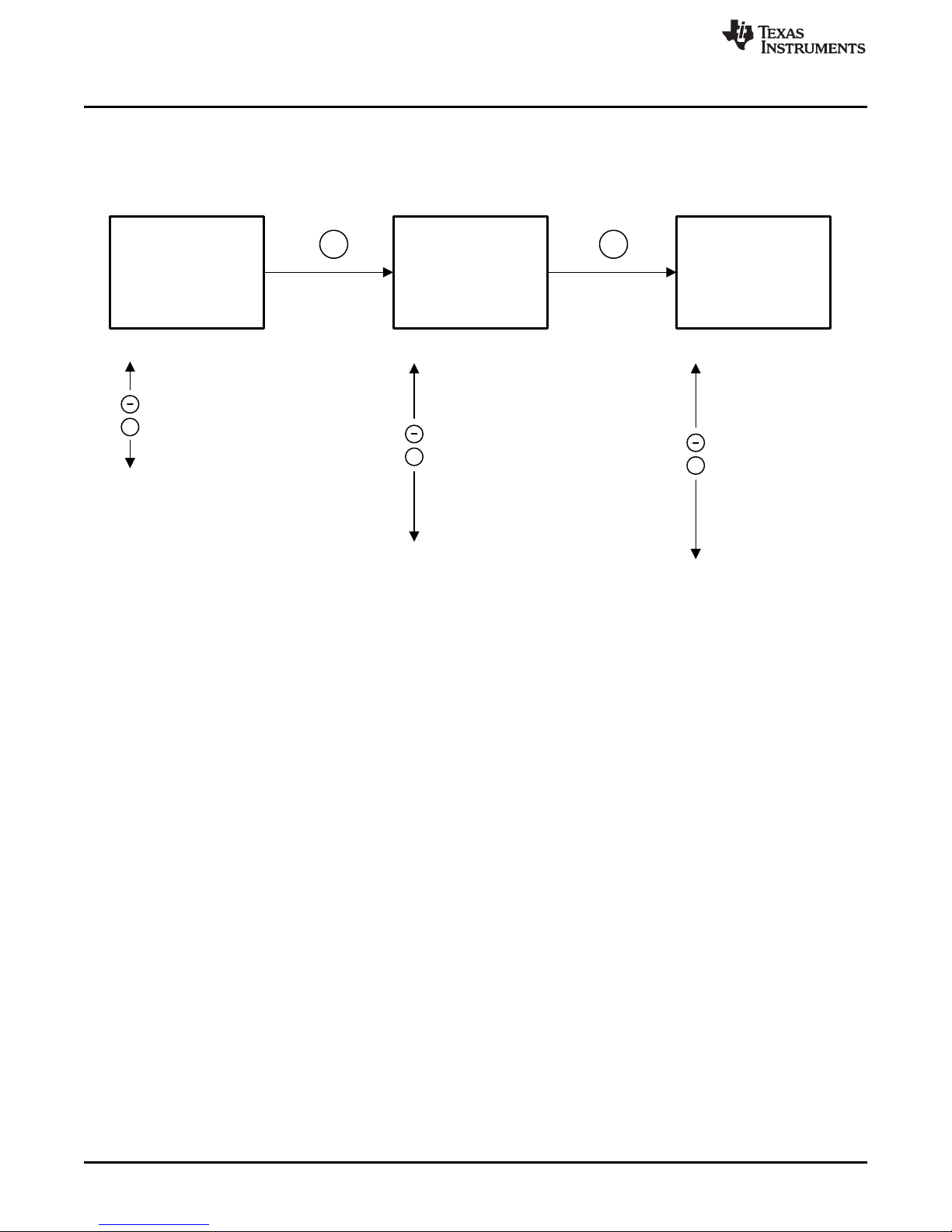
Demo Mode
ROM Library
Mode
Binary Counting
Mode
+ +
Hold for 3 s
Hold for 3 s
Modes
Mode OFF
Mode 4
Mode 3
.
.
Mode 0
Modes*
Mode 0
Mode 1
Mode 2
.
.
Mode 5
.
.
Mode 30
Mode 31 (Library Select)
Modes*
Mode 0
Mode 1
Mode 2
.
.
Mode 9
Mode 10 (Empty)
.
Mode 29 (Empty)
Mode 30
Mode 31
+
+
+
* Displayed in Binary
DRV2605L Demonstration Program
2 DRV2605L Demonstration Program
The DRV2605LEVM-CT contains a microcontroller and embedded software to control the DRV2605L.
There are three sets of modes accessible by pressing and holding the “+” button. Follow the instructions in
the following sections to access the effects in each set.
www.ti.com
6
DRV2605L ERM and LRA Haptic Driver Evaluation Kit SLOU389A–May 2014–Revised June 2014
Figure 2. DRV2605LEVM-CT Mode Sets
Copyright © 2014, Texas Instruments Incorporated
Submit Documentation Feedback
Page 7
www.ti.com
2.1 Demo Mode
Table 2 lists the effects preloaded on the DRV2605LEVM-CT. The modes are selected using the “+” and
“–“ mode buttons in the center of the board. The current mode can be identified by the white LEDs directly
above the mode buttons. Buttons B1 to B4 trigger the effects listed in the description column and change
based on the selected mode.
Mode Button Description Actuator Interface
Mode Off
LEDs Off
Mode 4
LED M4 On
Mode 3
LED M3 On
Mode 2
LED M2 On
Mode 1 The board gives several waveforms to match. ERM and
LED M1 On Must match from a given waveform list each LRA
Mode 0
LED M0 On
DRV2605L Demonstration Program
Table 2. Mode and Effects Table
Waveform
Location
B1 Click + Ramp Down
B2 Ramp Up + Pulsing
B3 Click + Ramp Down
B4 Ramp Up + Pulsing
B1 SharpClick_100 Internal trigger
B2 StrongClick_60 + Release External edge trigger
B3 SoftBump_100 Internal trigger
B4 DoubleClick_100 External level trigger
B1 SharpTick2_80 Internal trigger
B2 StrongClick_100 + Release External edge trigger
B3 SoftBump_100 Internal trigger
B4 DoubleClick_100 External level trigger
B1 LRA auto-resonance on RTP
B2 LRA auto-resonance off µController PWM
B3 ERM buzz alert (closed loop) RTP
B4 ERM buzz alert (open loop) ROM Internal trigger
B1
Matching Game:
B2
B3
time before going to the next given waveform.
B4
B1 Audio-to-haptics enable ERM
B2 Audio-to-haptics enable LRA
B3 Exit A2H, click, return to A2H
B4 Exit A2H, buzz, return to A2H
ERM
ROM
LRA
ERM ROM
LRA ROM
LRA
ERM
ROM
External analog
source
ERM and
LRA
ROM
Internal trigger (I2C)
Internal trigger (I2C)
Audio-to-haptics
Internal trigger (I2C)
SLOU389A–May 2014–Revised June 2014 DRV2605L ERM and LRA Haptic Driver Evaluation Kit
Submit Documentation Feedback
7
Copyright © 2014, Texas Instruments Incorporated
Page 8
DRV2605L Demonstration Program
2.2 Description of the Demo Modes
The following sections describe each demo mode in more detail.
2.2.1 Mode Off – Haptics Effect Sequences
Mode Off contains a set of haptic sequences that combine a series of haptic effects. The two following
effects show combinations of clicks, ramps, and pulses.
www.ti.com
Figure 3. ERM Click and Ramp-Down Waveform Figure 4. LRA Ramp-Up and Pulsing Waveform
(Button 1) (Button 4)
2.2.2 Mode 4 – ERM Clicks
Mode 4 shows two different ERM click styles. Button 1 shoes a single sharp click. Button 2 shows a click
and release effect. The click and release effect provides a haptic waveform on both the button press and
the button release.
Figure 5. ERM SharpClick_100 (Button 1) Figure 6. ERM StrongClick_60 and Release
SharpClick_100 (Button 2)
8
DRV2605L ERM and LRA Haptic Driver Evaluation Kit SLOU389A–May 2014–Revised June 2014
Copyright © 2014, Texas Instruments Incorporated
Submit Documentation Feedback
Page 9
www.ti.com
2.2.3 Mode 3 – LRA Clicks
Mode 3 shows two different LRA click styles. Button 1 shoes a single sharp click and Button 2 shows a
click and release effect. The click and release effect provides a haptic waveform on both the button press
and the button release.
Figure 7. LRA SharpTick2_80 (Button 1) Figure 8. LRA StrongClick 100 and Release SharpTick2
DRV2605L Demonstration Program
80 (Button 2)
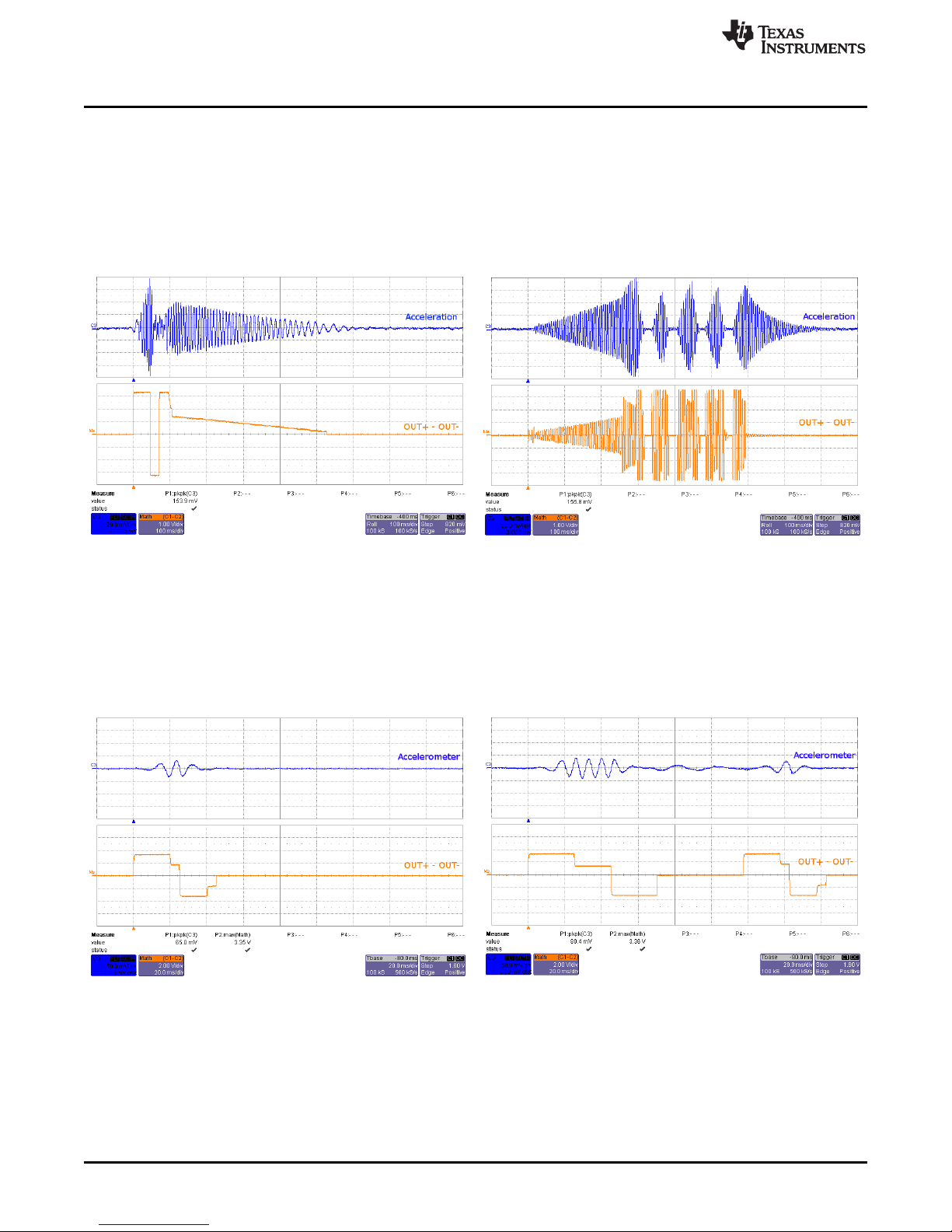
2.2.4 Mode 2 – Alerts
Mode 2 showcases the advantages of the smart loop architecture, which includes auto-resonance
tracking, automatic overdrive, and automatic braking.
Figure 9 and Figure 10 show the difference in acceleration when using LRA auto-resonance on and LRA
auto-resonance off. Notice that the acceleration is higher when driven at the resonant frequency. Also,
notice the start and stop time of the acceleration are much quicker when using the overdrive and braking
feature of the DRV2605L.
Figure 9. LRA Auto-Resonance On (Button 1) Figure 10. LRA Auto-Resonance Off (Button 2)
SLOU389A–May 2014–Revised June 2014 DRV2605L ERM and LRA Haptic Driver Evaluation Kit
Submit Documentation Feedback
9
Copyright © 2014, Texas Instruments Incorporated
Page 10
Acceleration (G)
Frequency (Hz)
DRV2605L Demonstration Program
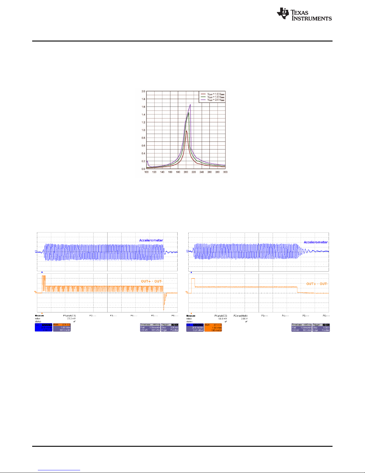
The reason for higher acceleration can be seen in Figure 11. The LRA has a very-narrow operating
frequency range due to the properties of a spring-mass system. Furthermore, the resonance frequency
drifts over various conditions such as temperature and drive voltage (the effects shown in Figure 11). With
the smart loop auto-resonance feature, the DRV2605L dynamically tracks the exact resonant frequency to
maximize the vibration force.
Figure 11. LRA Acceleration versus Frequency over Output Voltage
Figure 12 and Figure 13 show the difference between an ERM with automatic closed-loop overdrive and
braking, and the open-loop library waveform with a predefined overdrive period. The closed-loop version
starts and stops the actuator perfectly and does not drive too long or too short. Automatic overdrive and
braking simplify the design of haptic effects by eliminating the tuning time for actuator startup and stop.
www.ti.com
Figure 12. ERM Closed Loop (Button 3) Figure 13. ERM Open Loop (Button 4)
10
DRV2605L ERM and LRA Haptic Driver Evaluation Kit SLOU389A–May 2014–Revised June 2014
Copyright © 2014, Texas Instruments Incorporated
Submit Documentation Feedback
Page 11

www.ti.com
2.2.5 Mode 1 – Waveform Matching Game
Mode 1 is a game that incorporates the various LRA effects. This can be used to demonstrate haptics in a
real application.
To begin playing Matching:
1. Press any of the large effect buttons.
2. The game then counts down.
3. Once the countdown completes, a waveform will play from the LRA and the user must match that
given waveform from the given options list before going to the next waveform match.
• B1 - Play/repeat selected waveform from the options list
• B2 - Cycle through the waveforms in the options list to choose from
• B3 - Selects the guessed waveform (B1) as answer
• B4 - Play/repeat the given waveform
4. After each successfully successful match, the board will buzz from the LRA and count down to the next
given waveform. If the user selects incorrectly, then the ERM will buzz and the game is over. If the
user matches all of the given waveforms, the LEDs will scroll and flash twice.
DRV2605L Demonstration Program
SLOU389A–May 2014–Revised June 2014 DRV2605L ERM and LRA Haptic Driver Evaluation Kit
Submit Documentation Feedback
11
Copyright © 2014, Texas Instruments Incorporated
Page 12
DRV2605L Demonstration Program
2.2.6 Mode 0 – Audio-to-Haptics
Audio-to-haptics is a unique feature that converts an audio signal to haptics. Take audio from music,
games, or movies and automatically create haptic effects.
Buttons B1 to B4 perform the following actions:
• Button 1 – Audio-to-haptics using ERM
• Button 2 – Audio-to-haptics using LRA
• Button 3 – Switch to internal trigger and play library click effect
• Button 4 – Switch to internal trigger and play library buzz effect
To use this mode:
1. Connect an audio source to the audio jack on the left side of the board. The tip of the audio connector
is applied to the input of the DRV2605L.
2. Press button 1 which enables audio-to-haptics using the on-board ERM
3. Decrease the volume of the audio source, if the ERM is constantly vibrating, or increase the volume, if
the ERM is not vibrating at all.
4. Feel the haptic vibrations as the audio plays.
5. Press button 2 which enables audio-to-haptics using the on-board LRA.
6. Decrease the volume of the audio source if the LRA is constantly vibrating or increase the volume if
the LRA is not vibrating at all.
7. Feel the haptic vibrations as the audio plays.
8. Press button 3 or 4 to trigger a click or buzz during audio-to-haptics playback.
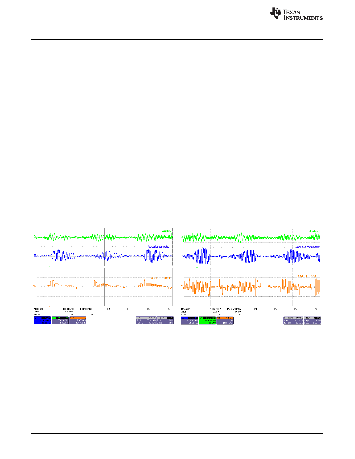
Figure 14 and Figure 15 show the conversion process from audio to hatpics for both ERM and LRA.
www.ti.com
Figure 14. ERM Audio-to-Haptics Conversion Figure 15. LRA Audio-to-Haptics Conversion
(Button 1) (Button 2)
12
DRV2605L ERM and LRA Haptic Driver Evaluation Kit SLOU389A–May 2014–Revised June 2014
Copyright © 2014, Texas Instruments Incorporated
Submit Documentation Feedback
Page 13

www.ti.com
2.3 ROM Library Mode
ROM library effects can be accessed by holding the "+" button until the mode LEDs flash and colored
LEDs flash once.
Once in "Library Mode," the DRV2605L embedded ROM effects can be accessed in sequential order. For
example, with all mode LEDs off, B1 is waveform 1, B2 is waveform 2, and so on. Then when mode LED
M0 is on, B1 is waveform 5, B2 is waveform 6, and so on.
The equations for calculating the mode and button of an effect are:
Mode = RoundDown([Effect No.] / 4)
Button = ([Effect No.] - 1) % 4 + 1
% - is the modulo operator
To change between the 5 ERM libraries and the Johnson Electric (JE) ROM Library:
1. Select mode 31 (11111'b) using the "+" or "–" buttons.
• B1 – Press repeatedly to access ROM libraries 1 through 5 and the JE ROM library. The current
library flashes on the mode LEDs
• B2 – Press to select the LRA ROM library
2. Then use the ROM effects as described previously
Each ERM library was designed for specific actuator behavior. Table 3 describes the actuator properties
that are best suited for each library. Note that the rated and overdrive voltages can be changed using the
rated and overdrive clamp registers in the DRV2605L. The most important parameters to characterize with
your actuator are the rise and brake times.
DRV2605L Demonstration Program
Table 3. DRV2605L Library Table
Number Library
1 Library A 1.3 3 40 – 60 20 – 40
2 Library B 3 3 40 – 60 5 – 15
3 Library C 3 3 60 – 80 10 – 20
4 Library D 3 3 100 – 140 15 – 25
5 Library E 3 3 >140 >30
7 Library F 4.5 5 35 – 45 10 – 20
Rated Voltage (V) Overdrive Voltage (V) Rise Time (ms) Brake Time (ms)
Actuator Properties
SLOU389A–May 2014–Revised June 2014 DRV2605L ERM and LRA Haptic Driver Evaluation Kit
Submit Documentation Feedback
13
Copyright © 2014, Texas Instruments Incorporated
Page 14

DRV2605L Demonstration Program
2.4 ROM Library Effects List
Below is a description of the 123 waveforms embedded in the DRV2605L.
www.ti.com
Effect Effect Effect
ID# ID# ID#
1 Strong click – 100% 42 Long double sharp click medium 2 – 80% 83 Transition ramp up long smooth 2 – 0 to 100%
2 Strong click – 60% 43 Long double sharp click medium 3 – 60% 84 Transition ramp up medium smooth 1 – 0 to 100%
3 Strong click – 30% 44 Long double sharp tick 1 – 100% 85 Transition ramp up medium smooth 2 – 0 to 100%
4 Sharp click – 100% 45 Long double sharp tick 2 – 80% 86 Transition ramp up short smooth 1 – 0 to 100%
5 Sharp click – 60% 46 Long double sharp tick 3 – 60% 87 Transition ramp up short smooth 2 – 0 to 100%
6 Sharp click – 30% 47 Buzz1 – 100% 88 Transition ramp up long sharp 1 – 0 to 100%
7 Soft bump – 100% 48 Buzz2 – 80% 89 Transition ramp up long sharp 2 – 0 to 100%
8 Soft bump – 60% 49 Buzz3 – 60% 90 Transition ramp up medium sharp 1 – 0 to 100%
9 Soft bump – 30% 50 Buzz4 – 40% 91 Transition ramp up medium sharp 2 – 0 to 100%
10 Double click – 100% 51 Buzz 5 – 20% 92 Transition ramp up short sharp 1 – 0 to 100%
11 Double click – 60% 52 Pulsing strong 1 – 100% 93 Transition ramp up short sharp 2 – 0 to 100%
12 Triple click – 100% 53 Pulsing strong 2 – 60% 94 Transition ramp down long smooth 1 – 50 to 0%
13 Soft fuzz – 60% 54 Pulsing medium 1 – 100% 95 Transition ramp down long smooth 2 – 50 to 0%
14 Strong buzz – 100% 55 Pulsing medium 2 – 60% 96 Transition ramp down medium smooth 1 – 50 to 0%
15 750-ms alert 100% 56 Pulsing sharp 1 – 100% 97 Transition ramp down medium smooth 2 – 50 to 0%
16 1000-ms alert 100% 57 Pulsing sharp 2 – 60% 98 Transition ramp down short smooth 1 – 50 to 0%
17 Strong click 1 – 100% 58 Transition click 1 – 100% 99 Transition ramp down short smooth 2 – 50 to 0%
18 Strong click 2 – 80% 59 Transition click 2 – 80% 100 Transition ramp down long sharp 1 – 50 to 0%
19 Strong click 3 – 60% 60 Transition click 3 – 60% 101 Transition ramp down long sharp 2 – 50 to 0%
20 Strong click 4 – 30% 61 Transition click 4 – 40% 102 Transition ramp down medium sharp 1 – 50 to 0%
21 Medium click 1 – 100% 62 Transition click 5 – 20% 103 Transition ramp down medium sharp 2 – 50 to 0%
22 Medium click 2 – 80% 63 Transition click 6 – 10% 104 Transition ramp down short sharp 1 – 50 to 0%
23 Medium click 3 – 60% 64 Transition hum 1 – 100% 105 Transition ramp down short sharp 2 – 50 to 0%
24 Sharp tick 1 – 100% 65 Transition hum 2 – 80% 106 Transition ramp up long smooth 1 – 0 to 50%
25 Sharp tick 2 – 80% 66 Transition hum 3 – 60% 107 Transition ramp up long smooth 2 – 0 to 50%
26 Sharp tick 3 – 60% 67 Transition hum 4 – 40% 108 Transition ramp up medium smooth 1 – 0 to 50%
27 Short double click strong 1 – 100% 68 Transition hum 5 – 20% 109 Transition ramp up medium smooth 2 – 0 to 50%
28 Short double click strong 2 – 80% 69 Transition hum 6 – 10% 110 Transition ramp up short smooth 1 – 0 to 50%
29 Short double click strong 3 – 60% 70 111 Transition ramp up short smooth 2 – 0 to 50%
30 Short double click strong 4 – 30% 71 112 Transition ramp up long sharp 1 – 0 to 50%
31 Short double click medium 1 – 100% 72 113 Transition ramp up long sharp 2 – 0 to 50%
32 Short double click medium 2 – 80% 73 114 Transition ramp up medium sharp 1 – 0 to 50%
33 Short double click medium 3 – 60% 74 115 Transition ramp up medium sharp 2 – 0 to 50%
34 Short double sharp tick 1 – 100% 75 116 Transition ramp up short sharp 1 – 0 to 50%
35 Short double sharp tick 2 – 80% 76 117 Transition ramp up short sharp 2 – 0 to 50%
36 Short double sharp tick 3 – 60% 77 118 Long buzz for programmatic stopping – 100%
37 78 119 Smooth hum 1 (No kick or brake pulse) – 50%
38 Long double sharp click strong 2 – 80% 79 120 Smooth hum 2 (No kick or brake pulse) – 40%
39 Long double sharp click strong 3 – 60% 80 121 Smooth hum 3 (No kick or brake pulse) – 30%
40 Long double sharp click strong 4 – 30% 81 122 Smooth hum 4 (No kick or brake pulse) – 20%
41 82 123 Smooth hum 5 (No kick or brake pulse) – 10%
Waveform Name Waveform Name Waveform Name
Transition ramp down long smooth 1 – 100
Transition ramp down long smooth 2 – 100
Transition ramp down medium smooth 1 –
Transition ramp down medium smooth 2 –
Transition ramp down short smooth 1 – 100
Transition ramp down short smooth 2 – 100
Transition ramp down long sharp 1 – 100 to
Transition ramp down long sharp 2 – 100 to
Long double sharp click strong 1 – Transition ramp down medium sharp 1 –
Long double sharp click medium 1 – Transition ramp up long smooth 1 – 0 to
100% 100 to 0%
Transition ramp down medium sharp 2 –
Transition ramp down short sharp 1 – 100
Transition ramp down short sharp 2 – 100
100% 100%
to 0%
to 0%
100 to 0%
100 to 0%
to 0%
to 0%
0%
0%
100 to 0%
to 0%
to 0%
14
DRV2605L ERM and LRA Haptic Driver Evaluation Kit SLOU389A–May 2014–Revised June 2014
Copyright © 2014, Texas Instruments Incorporated
Submit Documentation Feedback
Page 15

www.ti.com
3 Additional Hardware Modes
Additional modes are available on the DRV2605LEVM-CT that provide increased board control and
functionality. The additional modes are not available in “demo” mode, but can be accessed by switching to
“binary counting mode”. In “binary counting mode,” the mode LEDs count in binary (32 modes) rather than
in “demo” mode format (only six modes including off).
3.1 Enter Binary Counting Mode
To enter “binary counting mode” and access the additional modes:
1. Press and hold the increment mode button (“+”) for approximately 3 seconds until the mode LEDs flash
and the colored LEDs flash once.
2. Press and hold the increment mode button ("+") one more time until the mode LEDs flash and the
colored LEDs flash twice.
3. Select from the “binary counting modes” using the “+” and “–" buttons.
3.2 Exit Binary Counting Mode
To exit “binary counting mode” and return to “demo” mode:
1. Press and hold the decrement mode button (“–") for approximately 3 seconds.
2. Release the button when the actuator buzzes and mode LEDs flash.
3. Select from the “demo” modes using the “+” and "–" buttons.
Additional Hardware Modes
SLOU389A–May 2014–Revised June 2014 DRV2605L ERM and LRA Haptic Driver Evaluation Kit
Submit Documentation Feedback
15
Copyright © 2014, Texas Instruments Incorporated
Page 16

Additional Hardware Modes
3.3 Binary Counting Modes
Table 4 lists the modes available in “binary counting mode”.
Mode Button Description Notes
Mode 0
External I2C mode
LEDs: 00000
Mode 1
Auto-calibration and
diagnostics
LEDs: 00001
Mode 2 External PWM - disconnect MSP430 PWM using JP1. Connect
External PWM external PWM signal to the "PWM" test point at the top of the
LEDs: 00010 board. Select actuator using buttons B2 and B3.
Mode 3
External PWM and
enable
LEDs: 00011
Mode 4
Analog Input
LEDs: 00100
Mode 5 Vary the auto-resonance off (open-loop) output frequency and see
Auto-resonance OFF the change in vibration force over frequency. Hold B3 or B4 for
frequency adjust quick frequency adjustment. Compare B2 (auto-resonance off) with
LEDs:00101 B1 (auto-resonance on).
Mode 6
Life test (RTP)
2s ON, 1s OFF
LEDs: 00110
Mode 7 Life test using RTP (infinite buzz) - board must be powered down to
Life test (RTP) stop buzz. Increment or decrement amplitude using B3 and B4.
Infinite buzz Test new amplitude using B2 before beginning life test. Choose
LEDs: 00111 actuator using buttons B1 and B2 in mode 0 and mode 1.
Mode 8
Life test (PWM)
2s ON, 1s OFF
LEDs: 01000
Mode 9
Recorder
LEDs: 01001
Mode 11
Frequency Sweep
LEDs: 01011
Mode 12
2nd Cycle Test
LEDs: 01100
B1 SetERM output
B2 SetLRA output
B3 Choosetrigger
B4 Triggerbutton
B1 ERMauto-calibration
B2 LRAauto-calibration
B3 ERMdiagnostics Run diagnostics, 1 flash = successful, 3 flashes = error. The status
B4 LRAdiagnostics
B1 DisablePWM mode
B2 SetERM output
B3 SetLRA output
B4 –
B1 Returnto typical mode
B2 SetERM output
B3 SetLRA output
B4 –
B1 ACcoupling - ERM
B2 DCcoupling - ERM
B3 ACcoupling - LRA
B4 DCcoupling - LRA
B1 Alert(auto-resonance on)
B2 Alert(auto-resonance off)
B3 Decreaseoutput frequency
B4 Increaseoutput frequency
B1 Beginlife test
B2 Testbuzz
B3 Decreaseoutput voltage (–1)
B4 Increaseoutput voltage (+1)
B1 Beginlife test
B2 Testbuzz
B3 Decreaseoutput voltage (–1)
B4 Increaseoutput voltage (+1)
B1 Beginlife test
B2 Testbuzz
B3 Decreaseoutput voltage (–1)
B4 Increaseoutput voltage (+1)
B1 Startor stop recording
B2 Createeffect
B3 Startor stop play back
B4 –
B1 BuzzAlert@ Frequency
B2 BuzzAlert@ Resonance
B3 DecreaseFrequency (–1)
B4 IncreaseFrequency (+1)
B1 Nevertransition to open loop 2nd Cycle Test - for this mode, connect a resistor of 20 Ω (min of 8
B2 Auto-transitionto OL drive
B3
B4
www.ti.com
Table 4. Binary Counting Modes
Use this mode to control the DRV2605L using an external I2C
Master. Press B1 or B2 to choose between the ERM or LRA. Press
B3 to choose the trigger type. (1 - Internal, 2 - External edge, 3 External level). Press B4 to trigger the waveform sequencer.
Run the auto-calibration. The new auto-calibration results are used
for all board effects, 1 flash = successful, 3 flashes = error.
register bits [3:0] are displayed on the mode LEDs [3:0] when
complete.
External PWM and enable - disconnect MSP430 PWM using JP1.
Connect external PWM signal to the "PWM" test point at the top of
the board. Connect an external enable signal to the "EN" test point.
Select actuator using buttons B2 and B3. Press B1 before switching
modes.
Analog input - apply an external analog signal for AC coupling on
the "audio" jack. Apply a DC coupled signal to the "PWM" test point.
Life test using RTP (2 seconds on, 1 second off) - life test repeats
infinite times and board must be powered down to stop. Increment
or decrement amplitude using B3 and B4. Test new amplitude using
B2. Choose actuator using buttons B1 and B2 in mode 0 or mode
1.
Life test using PWM (2 seconds on, 1 second off) - life test repeats
infinite times and board must be powered down to stop. Increment
or decrement amplitude using B3 and B4. Test new amplitude using
B2. Choose actuator using buttons B1 and B2 in mode 0 or mode
1.
Recorder - use this mode to create a single amplitude pattern. Start
by pressing the record button (B1), then use B2 to create the
pattern by tapping the button. When finished, press the play back
button (B3).
Frequency Sweep (ROM Mode) - Increment or decrement the
frequency using B3 and B4. B1 - Start/stop buzz alert at chosen
frequency. B2 - Start/Stop buzz alert using auto-resonance.
Frequency range: (50 Hz – 300 Hz)
Ω, max of 25 Ω) to simulate the resistance of a frozen actuator. B1
plays a buzz alert with OL drive disabled. B2 plays a buzz alert with
the automatic transition to open loop drive enabled (when backEMF not detected). Demonstrates DRV2605L improved algorithm to
sync.
16
DRV2605L ERM and LRA Haptic Driver Evaluation Kit SLOU389A–May 2014–Revised June 2014
Submit Documentation Feedback
Copyright © 2014, Texas Instruments Incorporated
Page 17

www.ti.com
Table 4. Binary Counting Modes (continued)
Mode Button Description Notes
B1 5ms playback interval enabled
Mode 13
ROM Playback Interval
LEDs: 01101
Mode 30
Actuator break-in Actuator break-in - used to break in new actuators
LEDs: 11110
Mode 31
About the board
LEDs: 11111
B2 1ms playback interval enabled
B3 SelectsERM or LRA
B4
B1 Beginactuator break-in
B2
B3
B4
B1 DeviceID
B2 Siliconrevision
B3 Coderevision
B4
4 Hardware Configuration
The DRV2605LEVM-CT is flexible and can be used to completely evaluate the DRV2605L. The following
sections list the various hardware configurations.
4.1 Input and Output Overview
The DRV2605LEVM-CT allows complete evaluation of the DRV2605L though test points, jacks, and
connectors. Table 5 gives a brief description of the hardware.
Hardware Configuration
Playback interval - demonstrates the 1 ms or 5 ms playback
interval. Affects buzz waveform by multiplying the time data either
by 1 ms or 5 ms. B1 - 5 ms mode enabled, B2 - 1 ms mode
enabled, B3 - selects between ERM or LRA.
About the board - the value appears on the mode LEDs in binary.
DRV2605L Device ID = 00011
Signal Description I/O
PWM External input to DRV2605L IN/TRIG pin Input / Observe
EN External DRV2605L enable control Input / Observe
OUT+ / OUT– Output
OUT Unfiltered output terminal block, connect to actuator Output
USB USB power (5 V) Input
VBAT External supply power (2.5 to 5.5 V) Input
SBW MSP430 programming header Input / Output
I2C DRV2605L and MSP430 I2C bus Input / Output
Audio DRV2605L is in audio-to-haptics mode, audio from this jack is converted to Input
Filtered output test points for observation, connect to oscilloscope, or
measurement equipment
The audio jack is connected to the IN/TRIG pin of the DRV2605L. When the
haptics
Hardware configuration details can be found in the following sections.
4.2 Power Supply Selection
The DRV2605LEVM-CT can be powered by USB or an external power supply (VBAT). Jumpers “DRV”
and “MSP” are used to select USB or VBAT for the DRV2605L and MSP430G2553, respectively. See the
following table for possible configurations.
Table 5. Hardware Overview
SLOU389A–May 2014–Revised June 2014 DRV2605L ERM and LRA Haptic Driver Evaluation Kit
Submit Documentation Feedback
17
Copyright © 2014, Texas Instruments Incorporated
Page 18

100k
470pF
100k
470pF
OUT
OUT- OUT+
From DRV2605L
USB
VBAT
MSP
DRV
USB
VBAT
USB
VBAT
Hardware Configuration
www.ti.com
Figure 16. Power Jumper Selection
Supply Configuration DRV MSP DRV2605L Supply Voltage
USB – both USB USB 5 V
DRV2605L external supply, MSP430
USB
External Supply – both VBAT VBAT VBAT
USB with 3.3-V LDO
(1)
The DRV2605L supply must be on before operating the MSP430.
(2)
If a 3.3-V DRV2605L supply voltage is preferred while using the USB as the power source, remove R5 and add a 0-Ω resistor
(2)
– Both USB USB 3.3 V (R4 = Short, R5 = Open)
across R4.
4.3 Using an External Actuator
Figure 17. Terminal Block and Test Points
The DRV2605LEVM-CT can be used with an external actuator. Follow the instructions below to attach an
actuator to the "OUT" terminal block.
1. Remove jumpers JP3 and JP4, which disconnects the on-board actuators from the DRV2605L.
2. Attach the positive and negative leads of the actuator to the green “OUT” terminal block keeping in
mind polarity.
3. Screw down the terminal block to secure the actuator leads.
(1)
VBAT USB VBAT
NOTE: It is important to use the green terminal block when connecting an external actuator. The
"OUT+" and "OUT–" test points have low-pass filters and should only be used for
oscilloscope and bench measurements.
18
DRV2605L ERM and LRA Haptic Driver Evaluation Kit SLOU389A–May 2014–Revised June 2014
Copyright © 2014, Texas Instruments Incorporated
Submit Documentation Feedback
Page 19

JP1
VDD
DRV2605L
EN
IN/TRIG
GND
OUT+
OUT-
MSP430
PWM/
GPIO
P3.1
R8
EN PWM
SDA
SCL
SDA
SCL
C11
AUDIO
R40, 0Q
R41, NP
SDA SCL
R43, 0Q
www.ti.com
4.4 PWM Input
JP1 PWM Source
Shorted MSP430
Open External PWM using PWM test point
Hardware Configuration
Figure 18. External PWM Input
To control the DRV2605L using PWM follow the instructions below.
1. Enter Additional Hardware Modes.
2. Select Mode 2 (00010'b) using the increment mode button ("+").
• B1 - Disable amplifier
• B2 - ERM mode
• B3 - LRA mode
• B4 - No function
3. Choose either the on-board ERM or LRA using button B1 or B2.
4. Apply the PWM signal to the PWM test point at the top of the board.
SLOU389A–May 2014–Revised June 2014 DRV2605L ERM and LRA Haptic Driver Evaluation Kit
Submit Documentation Feedback
Copyright © 2014, Texas Instruments Incorporated
19
Page 20

JP1
VDD
DRV2605L
EN
IN/TRIG
GND
OUT+
OUT-
MSP430
PWM/
GPIO
P3.1
R8
EN PWM
SDA
SCL
SDA
SCL
C11
AUDIO
R40, 0Q
R41, NP
SDA SCL
R43, 0Q
Hardware Configuration
4.5 External Trigger Control
JP1 PWM Source
Shorted MSP430
Open External GPIO using PWM test point
www.ti.com
Figure 19. External Trigger Control
The DRV2605L internal waveform sequencer can be triggered by controlling the IN/TRIG pin. There are
two external trigger options: edge trigger and level trigger. See the datasheet for more information on
these input trigger modes.
In mode 0 in the Additional Hardware Modes section, the DRV2605L can be set in external trigger mode,
and then triggered by using the trigger button control on button B4, or alternatively by applying an external
trigger signal to the PWM test point.
4.5.1 MSP430 Trigger Control
1. Enter Additional Hardware Modes.
2. Select Mode 0 (00000’b) using the increment mode button (“+”).
• B1 - Select the on-board ERM
• B2 - Select the on-board LRA
• B3 - Trigger select (1 = Internal trigger, 2 = External edge, 3 = External level)
• B4 - Trigger the waveform sequence using the MSP430
3. Fill the waveform sequencer with waveforms using the external I2C port.
4. Choose either the on-board ERM or LRA using buttons B1 or B2.
5. Select either external edge (2) or external level (3) trigger using button B3. The trigger type appears in
binary on the mode LEDs.
6. Apply the trigger signal to the IN/TRIG pin by pressing button B4.
4.5.2 External Source Trigger Control
1. Remove jumper JP1.
20
2. Enter Additional Hardware Modes.
3. Select mode 0 (00000’b) using the increment mode button (“+”).
• B1 - Select the on-board ERM
DRV2605L ERM and LRA Haptic Driver Evaluation Kit SLOU389A–May 2014–Revised June 2014
Copyright © 2014, Texas Instruments Incorporated
Submit Documentation Feedback
Page 21
JP1
VDD
DRV2605L
EN
IN/TRIG
GND
OUT+
OUT-
MSP430
PWM/
GPIO
P3.1
R8
EN PWM
SDA
SCL
SDA
SCL
C11
AUDIO
R40, 0Q
R41, NP
SDA SCL
R43, 0Q
www.ti.com
• B2 - Select the on-board LRA
• B3 - Trigger Select (1 = Internal trigger, 2 = External edge, and 3 = External level)
• B4 - Trigger the waveform sequence using the MSP430
4. Fill the waveform sequencer with waveforms using the external I2C port.
5. Choose either the on-board ERM or LRA using buttons B1 or B2.
6. Select either external edge (2) or external level (3) trigger using button B3. The trigger type appears in
binary on the mode LEDs.
7. Apply the external logic signal to the PWM test point to trigger the waveform.
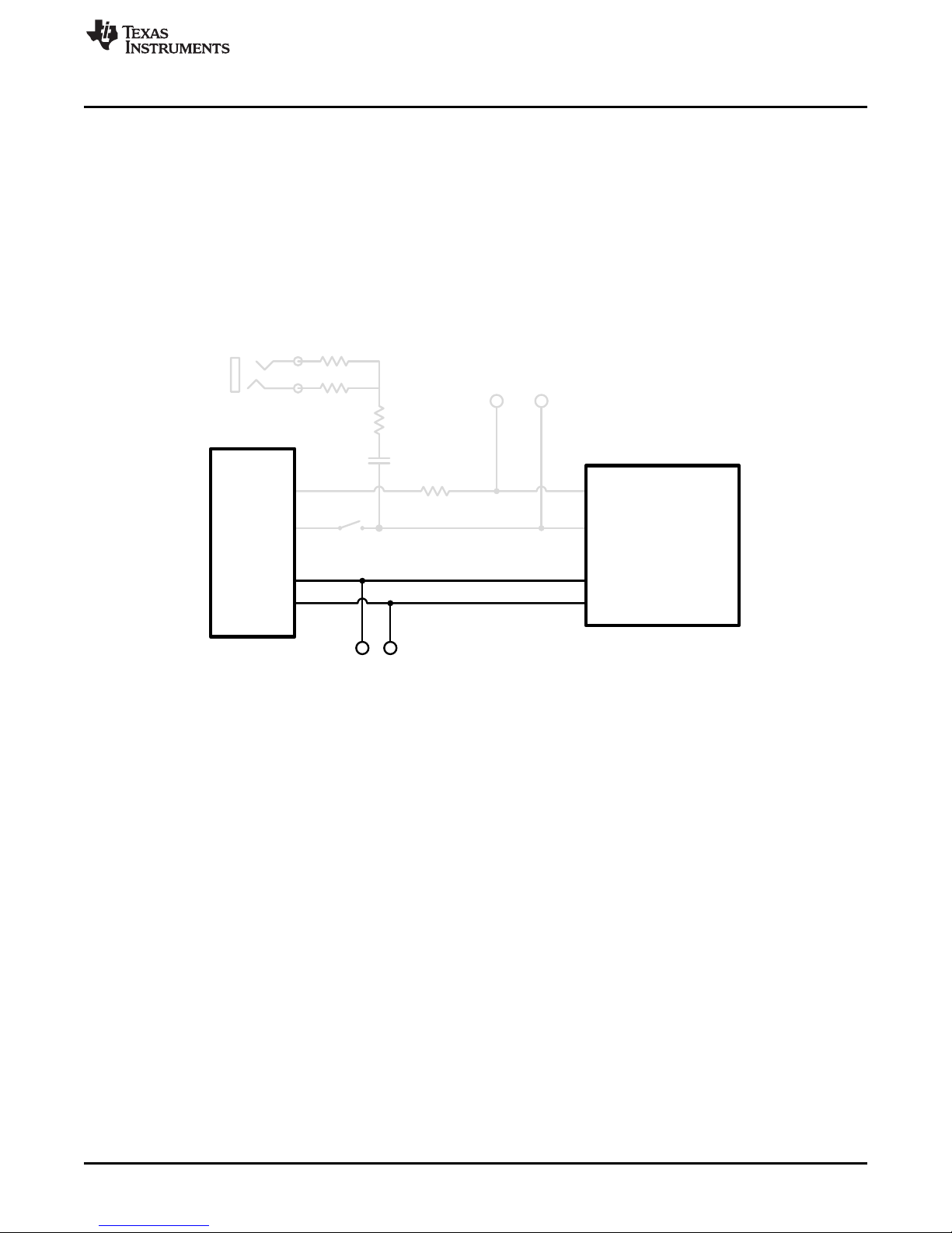
4.6 External I2C Input
Hardware Configuration
The DRV2605L can be controlled by an external I2C source. Attach the external controller to the I2C
header at the top of the board; be sure to connect SDA, SCL, and GND from the external source.
I2C communication is possible only when the EN pin is set high. To enable the DRV2605L and allow
external I2C control, follow these instructions:
1. Enter Additional Hardware Modes.
2. Select mode 0 (00000’b) using the increment mode button (“+”).
• B1 - Select the on-board ERM
• B2 - Select the on-board LRA
• B3 - Trigger Select (1 = Internal trigger, 2 = External edge, 3 = External level)
• B4 - Trigger the waveform sequence using the MSP430
3. Choose either the on-board ERM or LRA using buttons B1 or B2. Either button sets the EN pin high
and turns on the “Active” LED.
4. Begin controlling the DRV2605L using the external I2C source.
SLOU389A–May 2014–Revised June 2014 DRV2605L ERM and LRA Haptic Driver Evaluation Kit
Submit Documentation Feedback
Figure 20. External I2C Input
Copyright © 2014, Texas Instruments Incorporated
21
Page 22

JP1
VDD
DRV2605L
EN
IN/TRIG
GND
OUT+
OUT-
MSP430
PWM/
GPIO
P3.1
R8
EN PWM
SDA
SCL
SDA
SCL
C11
AUDIO
R40, 0Q
R41, NP
SDA SCL
R43, 0Q
Hardware Configuration
4.7 Audio-to-Haptics Input
The DRV2605L audio-to-haptics feature converts an audio signal to a corresponding haptics waveform.
This can be used to simulate bass in music, or use the audio track of a game to produce haptic effects.
To use audio-to-haptics:
1. Apply an analog line-out audio signal (not PWM) to the AUDIO jack on the left side of the board. The
tip of the inserted male audio plug is applied to the IN/TRIG pin of the DRV2605L. See Figure 21.
www.ti.com
Figure 21. Audio-to-Haptics Input
NOTE: To get the best performance using a headphone out, the user may need to adjust the
volume, so that the input signal is near, but does not exceed 1.8 V
2. In demo mode, select mode 0 (00001’b) using the increment mode button (“+”).
3. In mode 0, press either button B1 or B2 to enable the DRV2605L audio-to-haptics. Buttons B3 and B4
switch to internal trigger mode, play a ROM library effect, and then switch back to audio-to-haptics
mode.
• B1 – Audio-to-haptics using ERM
• B2 – Audio-to-haptics using LRA
• B3 – Switch to internal trigger and play library click effect
• B4 – Switch to internal trigger and play library buzz effect
4. Play music and feel the vibrations of the actuator.
22
NOTE: Some audio signals are too large or too small and the volume must be adjusted. Adjust
DRV2605L ERM and LRA Haptic Driver Evaluation Kit SLOU389A–May 2014–Revised June 2014
appropriately so that the maximum input voltage is 1.8 V and the bass of the input signal can
be felt on the actuator. The audio input minimum and maximum thresholds can be adjusted
using I2C. See the datasheet for more details.
Copyright © 2014, Texas Instruments Incorporated
peak
.
Submit Documentation Feedback
Page 23

ERM
Or
LRA
OUT+
OUT-
100k
100k
470 pF
470 pF
Ch1-Ch2
(Differential)
Oscilloscope
Ch1
Ch2
100k
470pF
100k
470pF
OUT
OUT- OUT+
From DRV2605L
www.ti.com
5 Measurement and Analysis
The DRV2605L uses PWM modulation to create the output signal for both ERM and LRA actuators. To
measure and observe the DRV2605L output waveform, connect an oscilloscope or other measurement
equipment to the filtered output test points, “OUT+” and “OUT–".
Figure 22. Terminal Block and Test Points
The DRV2605L drives LRA and ERM actuators using a 20-kHz PWM modulated waveform, but only the
frequencies around the LRA resonant frequency, or the ERM DC drive voltage, are relevant to the haptic
actuator vibration. The higher frequency switching content does not contribute to the vibration strength of
the actuator and can make it difficult to interpret the modulated output waveform on an oscilloscope. The
oscilloscope image Figure 23 shows the DRV2605L unfiltered waveform and Figure 24 shows a filtered
version used for observation and measurement.
Measurement and Analysis
Figure 23. DRV2605L Unfiltered Waveform Figure 24. DRV2605L Filtered Waveform
If the DRV2605LEVM-CT filter is not used, TI recommends using a first-order, low-pass filter with a cutoff
between 1 and 3.5 kHz. Figure 25 shows a recommended output filter for use while measuring and
characterizing the DRV2605L in the lab.
SLOU389A–May 2014–Revised June 2014 DRV2605L ERM and LRA Haptic Driver Evaluation Kit
Submit Documentation Feedback
Figure 25. Measuring the DRV2605L Output Signal With an Analog Low-Pass Filter
Copyright © 2014, Texas Instruments Incorporated
23
Page 24

EMULATION
Actuators
DRV2605L
MSP430
OUT
USB
VBAT
SBW
MSP
DRV
AUDIO
JP4
JP3
MSP-EXP430G2
MSP430 Firmware
6 MSP430 Firmware
The MSP430 firmware on the DRV2605LEVM-CT can be modified or reprogrammed to create new haptic
effects or behaviors. Find the latest firmware source code and binaries on www.ti.com. Follow these
instructions to modify or reprogram the DRV2605LEVM-CT:
1. Purchase one of the following MSP430G2553 compatible programmers:
• MSP430 LaunchPad (MSP-EXP430G2) – requires the additional purchase of a header for J4
(recommended)
– Digi-Key: ED8650-ND
– Mouser: 575-500201
• MSP430-FET430UIF – requires a JTAG to Spy-Bi-Wire adapter (MSP-JTAGSBW if available)
2. Download and install Code Compose Studio (CCS), or IAR Embedded Workbench IDE.
3. Download the DRV2605LEVM-CT source code and binaries from www.ti.com.
4. Connect the programmer to an available USB port.
5. Connect the programmer to the “SBW” header on the DRV2605LEVM-CT.
6. In CCS,
(a) Open the project file by selecting Project → Import Existing CCS Project.
(b) Select Browse and navigate to the DRV2605LEVM-CT project folder, then press OK.
(c) Select the checkbox next to the DRV2605LEVM-CT project in the “Discovered projects” window,
and then press Finish.
(d) Before compiling, navigate to Project → Properties → Build → MSP430 Compiler → Advanced
Options → Language Options, and make sure the checkbox for “Enable support for GCC
extensions (--gcc)” is checked.
7. In IAR,
(a) Create a new MSP430 project in IAR
(b) Select the MSP430G2553 device
(c) Copy the files in the project folder downloaded from www.ti.com to the new project directory
Figure 26 shows the connection between the MSP430 LaunchPad (MSP-EXP430G2) and the
DRV2605LEVM-CT.
www.ti.com
Figure 26. LaunchPad Programmer Connection
24
DRV2605L ERM and LRA Haptic Driver Evaluation Kit SLOU389A–May 2014–Revised June 2014
Copyright © 2014, Texas Instruments Incorporated
Submit Documentation Feedback
Page 25

www.ti.com
6.1 MSP430 Pinout
The DRV2605LEVM-CT contains a MSP430G2553 low-cost microcontroller, which controls the board and
contains sample haptic effects. The pinout for the microcontroller can be found in Table 6.
MSP430 Firmware
Table 6. MSP430 Pinout
NO. NAME DESCRIPTION
1 P1.1 Green LED
2 P1.2 Yellow LED
3 P1.3 Blue LED
4 P1.4 VREF+
5 P1.5 Audio-to-haptics
6 P3.1 Enable
7 P3.0 Actuator mode selection
8 NC
9 P2.0 Button 1
10 P2.1 Button 2
11 P2.2 Button 3
12 P3.2 PWM
13 P3.3 WLED 0
14 P3.4 WLED 1
15 P2.3 Button 4
16 P2.4 "+" button
17 P2.5 "–" button
18 P3.5 WLED 2
19 P3.6 WLED 3
20 P3.7 WLED 4
21 P1.6/SCL I2C Clock
22 P1.7/SDA I2C Data
23 SBWTDIO Spy-Bi-Wire data
24 SBWTCK Spy-Bi-Wire clock
25 P2.7
26 P2.6 LRA/ERM load switch
27 AVSS Analog ground
28 DVSS Digital ground
29 AVCC Analog supply
30 DVCC Digital supply
31 P1.0 Red LED
32 NC
SLOU389A–May 2014–Revised June 2014 DRV2605L ERM and LRA Haptic Driver Evaluation Kit
Submit Documentation Feedback
25
Copyright © 2014, Texas Instruments Incorporated
Page 26

SDA
SCL
SBWTDIO
WLED3
SCL-IN
WLED3
WLED4
BTN5
WLED2
BTN4
BTN3
WLED0
WLED1
WLED2
WLED1
BTN2
BTN1
BTN0
BTN5
BTN4
BTN3
BTN2
BTN1
BTN0
Audio2Haptics
SCL
SDA
SDA-IN
WLED4
WLED0
LoadSwitch
LoadSwitch
SBW
GND
Vbat
GND
GND
GND
Black
GND
+3.3V
GND
+3.3V
R7
0402
9.76K
+3.3V
C10
0402
0.1 / 6.3 VµF
C6
0805
10µF / 16 V
GND
C7
0402
1.0 / 6.3 VµF
GND
VBAT
Green
6A / 125 V
+3.3V
TXS0102DCT
U4
SSOP8-DCT
GND
C9
0402
0.1 / 6.3 VµF
GND
0402
0.0
R8
C5
TCT-TANT1206
100 / 6.3 VµF
+
GND
I2C
GND
GND
ACTIVE
0603
Green
JP2
+3.3V
C8
0402
0.1 / 6.3 VµF
0402
511
R9
JP1
GND
GND
ENIN
Orange
PWM
Orange
GND
511
0402
R13
GND
0402
511
R11
GND
0402
511
R12
GND
0402
511
R14
GND
White
0603
M3
GND
White
0603
M2
GND
White
0603
M1
GND
White
0603
M0
TP1
Black
GND
0805
Red
B1
0805
Green
B2
0805
Yellow
B3
Blue
0805
B4
GND
Green
0603
5V
GND
R26
1.5 kΩ
0402
USB MINIB
USB
0805
600Ω / 2 A
FB1
0805
600 / 2 AΩ
FB2
R20
DNP
0402
R21
0402
DNP
R22
DNP
0402
R23
0402
DNP
R24
DNP
0402
R25
0402
DNP
GND
+5 V-USB
DRV
MSP
GND
OUT
6A / 125 V
Green
1.0 µF/ 16 V
0402
C1
GND
Vbat
+5 V-USB
0.0
0603
R5
0603
DNP
R4
249
0402
R16 R17
0402
249
R18
249
0402
R19
0402
249
U3
3.3V / 400 mA
TPS73633DBV
GND
M4
0603
White
R15
0402
249
TS5A12301EYFPR
U5
WCSP6-YFP
GND
LRA_OUT+
LRA_OUT-
JP3
R31
DNP
0402
R30
0402
DNP
R32
0.0
0402
Vbat
C12
0402
0.1µF / 16 V
GND
Audio
SJ-3523-SMT
3.5mm
GND
R40
0402
0.0
R41
0402
DNP
R42
0402
DNP
GND
R33
0402
0.0
JP4
QFN32-RHB
U2
GND
AVM1
-
+
0402
0.0
R34
DNP
0402
R35
Vbat
0.0
0402
R36
GND
C2
0402
1.0 µF/ 16 V
GND
U1
WCSP9-YZF
IN/TRIG
EN
SDA
VREG
OUT-
OUT+
SCL
VBAT
GND
QFN32-RHB
U2
MSP430G2553RHB
P2.5
P3.5
P3.7
P1.6/SCL
P1.7/SDA
P3.6
SBWTDIO
SBWTCK
P1.0
NC
DVSS
AVSS
DVCC
P2.7
P2.6
AVCC
P1.1
P3.1
P1.5
P3.0
P1.4
P1.2
P1.3
NC
P2.0
P2.1
P3.2
P2.2
P2.3
P2.4
P3.4
P3.3
0.0
0402
R43
Orange
OUT+
0402
100 k /5%Ω
R50
470pF / 50 V
0402 X7R
C14
GND
Orange
OUT-
0402
100 k /5%Ω
R51
470pF / 50V
0402 X7R
C15
GND
C11
0402 X5R
0.1 / 6.3 VµF
LRA
ERM
ERM/LRA ACTUATOR
SWITCH
CAPTOUCH RESISTORS
DRV2605LYZF CAPTOUCH EVK
EXT INPUT
USB POWER
3.6 V - 5.5 V
POWER
SUPPLY
MODE SELECT LEDS
DRV2605L
MSP / DRV
1-2: VBAT POWER
2-3: USB POWER
Audio-to-Haptics
SBYBIWIRE
Schematic
www.ti.com
7 Schematic
Figure 27 illustrates the EVM schematic.
Figure 27. DRV2605LEVM-CT Schematic
26
DRV2605L ERM and LRA Haptic Driver Evaluation Kit SLOU389A– May 2014–Revised June 2014
Submit Documentation Feedback
Copyright © 2014, Texas Instruments Incorporated
Page 27

www.ti.com
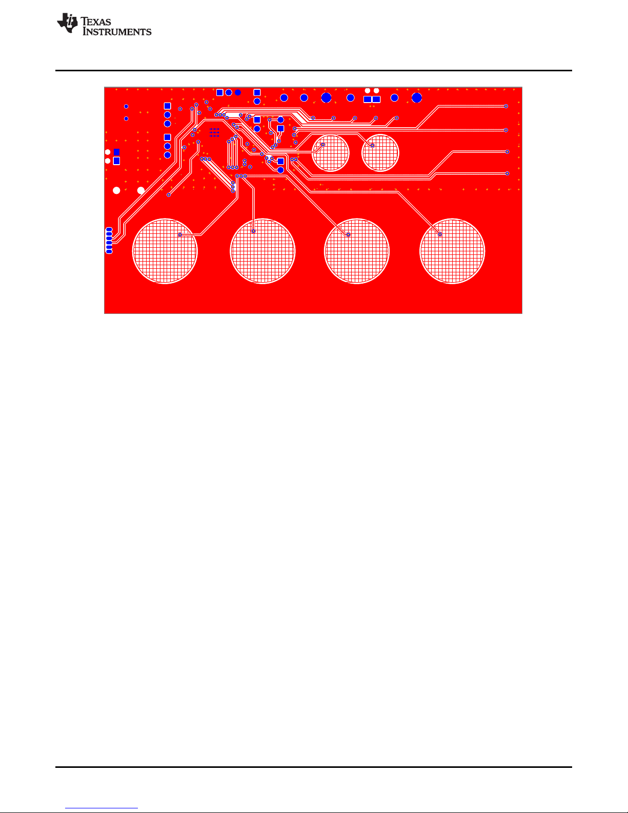
8 Layout
Layout
Figure 28. X-Ray Top View
spacer
Figure 29. Top Copper
SLOU389A–May 2014–Revised June 2014 DRV2605L ERM and LRA Haptic Driver Evaluation Kit
Submit Documentation Feedback
27
Copyright © 2014, Texas Instruments Incorporated
Page 28

Layout
www.ti.com
Figure 30. Layer 2 Copper
spacer
28
DRV2605L ERM and LRA Haptic Driver Evaluation Kit SLOU389A–May 2014–Revised June 2014
Figure 31. Layer 3 Copper
Copyright © 2014, Texas Instruments Incorporated
Submit Documentation Feedback
Page 29
www.ti.com
Layout
Figure 32. Bottom Copper
SLOU389A–May 2014–Revised June 2014 DRV2605L ERM and LRA Haptic Driver Evaluation Kit
Submit Documentation Feedback
29
Copyright © 2014, Texas Instruments Incorporated
Page 30

Bill of Materials
www.ti.com
9 Bill of Materials
Table 7 lists the bill of materials.
Table 7. Bill of Materials
Item MFR Part Number QTY Ref Designators Vendor Part Number Description MFR
Semiconductors
1 DRV2605LYZF 1 U1 DRV2605LYZF HAPTIC DRIVER AUTO DETECT FOR LRA AND ERM WCSP9-YZF TEXAS INSTRUMENTS
ROHS
2 TXS0102DCTR 1 U4 296-21978-1 2-BIT BIDIR LEVEL TRANSLATOR SSOP8-DCT ROHS TEXAS INSTRUMENTS
3 MSP430G2553IRHB32T 1 U2 595-P430G2553IRHB32T MIXED SIGNAL MICRO 16KB FLASH 512B RAM QFN32-RHB ROHS TEXAS INSTRUMENTS
4 TPS73633MDBVREP 1 U3 296-21283-1 VOLT REG 3.3V 400MA LDO CAP FREE NMOS SOT23-DBV5 TEXASINSTRUMENTS
ROHS
5 TS5A12301EYFPR 1 U5 296-23757-1-ND IEC LEVEL 4 ESD-PROTECTED 0.75-OHM ANALOG SWITCH TEXAS INSTRUMENTS
WCSP6-YFP ROHS
6 LTST-C190KGKT 2 5V, ACTIVE 160-1435-1-ND LED,GREEN,2.0V,SMD0603,ROHS LITE-ON INC.
7 LNJ037X8ARA 5 M0, M1, M2, M3, M4 LNJ037X8ARACT-ND LED, WHITE 2.9V SMD0805 ROHS PANASONIC
8 SML-LXT0805SRW-TR 1 B1 67-1555-1 LED, RED 2.0V SMD0805 ROHS LUMEX OPTO
9 SML-LXT0805GW-TR 1 B2 67-1553-1 LED, GREEN 2.0V SMD0805 ROHS LUMEX OPTO
10 SML-LXT0805YW-TR 1 B3 67-1554-1 LED, YELLOW 2.0V SMD0805 ROHS LUMEX OPTO
11 LTST-C171TBKT 1 B4 160-1645-1-ND LED, BLUE 3.3V SMD0805 ROHS LITE-ON INC.
Capacitors
12 GRM155R71C104KA88D 1 C12 490-3261-1-ND CAP SMD0402 CERM 0.1UFD 16V X7R 10% ROHS MURATA
13 C1005X5R1C105K050BC 2 C1, C2 445-4978-1-ND CAP SMD0402 CERM 1.0UFD 16V 10% X5R ROHS TDK CORP
14 C1005X5R0J104K 3 C8, C9, C10 445-1266-1 CAP SMD0402 CERM 0.1UFD 6.3V 10% X5R ROHS TDK CORP
15 0805YD106KAT2A 1 C6 478-5165-1 CAP SMD0805 CERM 10UFD 16V X5R 10% ROHS AVX
16 GRM155R60J105KE19D 1 C7 490-1320-1 CAP SMD0402 CERM 1.0UFD 6.3V X5R 10% ROHS MURATA
17 C1005X5R0J104K 1 C11 445-1266-1 CAP SMD0402 CERM 0.1UFD 6.3V 10% X5R ROHS TDK CORP
18 C0402C471K5RACTU 2 C14, C15 399-1025-1 CAP SMD0402 CERM 470PFD 50V 10% X7R ROHS KEMET
19 TCTAL0J107M8R 1 C5 511-1498-1-ND CAP TANT1206 100UFD 6.3V 20% TCT SERIES ROHS ROHM
Resistors
20 ERJ-2RKF9761X 1 R7 P9.76KLCT-ND RESISTOR SMD0402 THICK FILM 9.76K OHMS 1/10W 1% ROHS PANASONIC
21 RMCF0402ZT0R00 5 R8, R32, R33, R34, RMCF0402ZT0R00CT ZERO OHM JUMPER SMT 0402 0 OHM 1/16W,5% ROHS STACKPOLE ELECTRONICS
R36
22 RC0402FR-07511RL 5 R9, R11, R12, R13, 311-511LRCT-ND RESISTOR SMD0402 THICK FILM 511 OHMS 1% 1/16W ROHS YAGEO
R14
23 ERJ-2GEJ152 1 R26 RESISTOR,SMT,0402,THICK FILM,5%,1/16W,1.5K Panasonic
24 RMCF0603ZT0R00 1 R5 RMCF0603ZT0R00CT-ND RESISTOR SMD0603 ZERO OHMS 1/10W ROHS STACKPOLE ELECTRONICS
25 ERJ-2RKF2490X 5 R15, R16, R17, R18, P249LTR-ND RESISTOR,SMT,0402,249 OHM,1%,1/16W Panasonic
R19
26 CRCW04020000Z0ED 2 R40, R43 541-0.0JCT ZERO OHM JUMPER SMT 0402 0 OHM 1/16W,5% ROHS VISHAY
27 ERJ-2GEJ104 2 R50, R51 P100KJCT RESISTOR SMD0402 THICK FILM 100K OHMS 1/16W 5% ROHS PANASONIC
30
DRV2605L ERM and LRA Haptic Driver Evaluation Kit SLOU389A– May 2014–Revised June 2014
Submit Documentation Feedback
Copyright © 2014, Texas Instruments Incorporated
Page 31

www.ti.com
Bill of Materials
Table 7. Bill of Materials (continued)
Item MFR Part Number QTY Ref Designators Vendor Part Number Description MFR
Ferrite Beads
28 MPZ2012S601A 2 FB1, FB2 445-2206-1 FERRITE BEAD SMD0805 600 Ohms 2A ROHS TDK
Headers, Jacks, and Shunts
29 LPPB061NGCN-RC 1 SBW S9010E-06 HEADER THRU FEMALE 1X6-RA 50LS GOLD ROHS SULLINS
30 PBC03SAAN 3 DRV, I2C, MSP S1011E-03-ND HEADER THRU MALE 3 PIN 100LS GOLD ROHS SULLINS
31 PBC02SAAN 1 JP2 S1011E-02 HEADER THRU MALE 2 PIN 100LS GOLD ROHS SULLINS
32 PBC02SAAN 3 JP1, JP3, JP4 HEADER THRU MALE 2 PIN 100LS GOLD ROHS SULLINS
33 UX60-MB-5ST 1 USB H2959CT JACK USB MINIB SMT-RA 5PIN ROHS HIROSE
34 SJ-3523-SMT 1 Audio CP-3523SJCT-ND JACKAUDIO-STEREO MINI(3.5MM ,3-COND SMT-RA ROHS CUISTACK
35 SPC02SYAN 6 MSP (2-3), DRV (2- S9001-ND SHUNT BLACK AU FLASH 0.100LS CLOSED TOP ROHS SULLINS
3), JP1, JP2, JP3,
JP4
36 1725656 2 OUT, VBAT 277-1273 TERMINAL BLOCK MPT COMBICON 2PIN 6A/125V GREEN 100LS PHOENIX CONTACT
ROHS
Test Points and Switches
37 5011 2 GND, TP1 (Solder so 5011K PC TESTPOINT BLACK 063 HOLE ROHS KEYSTONE ELECTRONICS
that color ring is
secured)
38 5003 4 PWM, ENIN, OUT+, 5003K PC TESTPOINT, ORANGE, ROHS KEYSTONE ELECTRONICS
OUT– (Solder so that
color ring is secured)
39 NRS-2574 1 AVM1 NRS-2574 ACUTATOR VIBRATION MOTOR 1,3V 9000 RPM ROHS SANYO
40 SEMCO1030 1 - - ACTUATOR - LINEAR VIBRATOR, 2VRMS SAMSUNG
40
(1)
ELV1036 - - - AlternateACTUATOR – LINEAR VIBRATOR, 2VRMS AAC
42 3-5-468MP 1 - 3M9724-ND TAPE TRANSFER ADHESIVE 3" X 5YD 3M
43 2-5-4466W 1 - 3M9962-ND TAPE POLY FOAM 2" x 5YD 3M
Components Not Assembled
44 TestPoint_SMD- 2 LRA_OUT+,LRA_OU TESTPOINT SMD SQUARE 2.0mm
Square_2.0mm T–
45 R0402_DNP 9 R20, R21, R22, R23, R0402_DNP
R24, R25, R30, R31,
R35
46 R0603_DNP 1 R4 RMCF0603ZT0R00CT-ND R0603_DNP STACKPOLE ELECTRONICS
47 R0402_DNP 1 R41 P4.99KLCT-ND R0402_DNP PANASONIC
48 R0402_DNP 1 R42 541-0.0JCT R0402_DNP VISHAY
(1)
This is an alternate actuator used on the EVM.
31
SLOU389A– May 2014–Revised June 2014 DRV2605L ERM and LRA Haptic Driver Evaluation Kit
Submit Documentation Feedback
Copyright © 2014, Texas Instruments Incorporated
Page 32

Revision History
www.ti.com
Revision History
Changes from Original (May 2014) to A Revision ........................................................................................................... Page
• Changed C1 designator value to 1.0 µF in the schematic.......................................................................... 26
• Changed C1 from item 12 to item 13 in BOM........................................................................................ 30
32
Revision History SLOU389A–May 2014–Revised June 2014
Copyright © 2014, Texas Instruments Incorporated
Submit Documentation Feedback
Page 33

ADDITIONAL TERMS AND CONDITIONS, WARNINGS, RESTRICTIONS, AND DISCLAIMERS FOR
EVALUATION MODULES
Texas Instruments Incorporated (TI) markets, sells, and loans all evaluation boards, kits, and/or modules (EVMs) pursuant to, and user
expressly acknowledges, represents, and agrees, and takes sole responsibility and risk with respect to, the following:
1. User agrees and acknowledges that EVMs are intended to be handled and used for feasibility evaluation only in laboratory and/or
development environments. Notwithstanding the foregoing, in certain instances, TI makes certain EVMs available to users that do not
handle and use EVMs solely for feasibility evaluation only in laboratory and/or development environments, but may use EVMs in a
hobbyist environment. All EVMs made available to hobbyist users are FCC certified, as applicable. Hobbyist users acknowledge, agree,
and shall comply with all applicable terms, conditions, warnings, and restrictions in this document and are subject to the disclaimer and
indemnity provisions included in this document.
2. Unless otherwise indicated, EVMs are not finished products and not intended for consumer use. EVMs are intended solely for use by
technically qualified electronics experts who are familiar with the dangers and application risks associated with handling electrical
mechanical components, systems, and subsystems.
3. User agrees that EVMs shall not be used as, or incorporated into, all or any part of a finished product.
4. User agrees and acknowledges that certain EVMs may not be designed or manufactured by TI.
5. User must read the user's guide and all other documentation accompanying EVMs, including without limitation any warning or
restriction notices, prior to handling and/or using EVMs. Such notices contain important safety information related to, for example,
temperatures and voltages. For additional information on TI's environmental and/or safety programs, please visit www.ti.com/esh or
contact TI.
6. User assumes all responsibility, obligation, and any corresponding liability for proper and safe handling and use of EVMs.
7. Should any EVM not meet the specifications indicated in the user’s guide or other documentation accompanying such EVM, the EVM
may be returned to TI within 30 days from the date of delivery for a full refund. THE FOREGOING LIMITED WARRANTY IS THE
EXCLUSIVE WARRANTY MADE BY TI TO USER AND IS IN LIEU OF ALL OTHER WARRANTIES, EXPRESSED, IMPLIED, OR
STATUTORY, INCLUDING ANY WARRANTY OF MERCHANTABILITY OR FITNESS FOR ANY PARTICULAR PURPOSE. TI SHALL
NOT BE LIABLE TO USER FOR ANY INDIRECT, SPECIAL, INCIDENTAL, OR CONSEQUENTIAL DAMAGES RELATED TO THE
HANDLING OR USE OF ANY EVM.
8. No license is granted under any patent right or other intellectual property right of TI covering or relating to any machine, process, or
combination in which EVMs might be or are used. TI currently deals with a variety of customers, and therefore TI’s arrangement with
the user is not exclusive. TI assumes no liability for applications assistance, customer product design, software performance, or
infringement of patents or services with respect to the handling or use of EVMs.
9. User assumes sole responsibility to determine whether EVMs may be subject to any applicable federal, state, or local laws and
regulatory requirements (including but not limited to U.S. Food and Drug Administration regulations, if applicable) related to its handling
and use of EVMs and, if applicable, compliance in all respects with such laws and regulations.
10. User has sole responsibility to ensure the safety of any activities to be conducted by it and its employees, affiliates, contractors or
designees, with respect to handling and using EVMs. Further, user is responsible to ensure that any interfaces (electronic and/or
mechanical) between EVMs and any human body are designed with suitable isolation and means to safely limit accessible leakage
currents to minimize the risk of electrical shock hazard.
11. User shall employ reasonable safeguards to ensure that user’s use of EVMs will not result in any property damage, injury or death,
even if EVMs should fail to perform as described or expected.
12. User shall be solely responsible for proper disposal and recycling of EVMs consistent with all applicable federal, state, and local
requirements.
Certain Instructions. User shall operate EVMs within TI’s recommended specifications and environmental considerations per the user’s
guide, accompanying documentation, and any other applicable requirements. Exceeding the specified ratings (including but not limited to
input and output voltage, current, power, and environmental ranges) for EVMs may cause property damage, personal injury or death. If
there are questions concerning these ratings, user should contact a TI field representative prior to connecting interface electronics including
input power and intended loads. Any loads applied outside of the specified output range may result in unintended and/or inaccurate
operation and/or possible permanent damage to the EVM and/or interface electronics. Please consult the applicable EVM user's guide prior
to connecting any load to the EVM output. If there is uncertainty as to the load specification, please contact a TI field representative. During
normal operation, some circuit components may have case temperatures greater than 60°C as long as the input and output are maintained
at a normal ambient operating temperature. These components include but are not limited to linear regulators, switching transistors, pass
transistors, and current sense resistors which can be identified using EVMs’ schematics located in the applicable EVM user's guide. When
placing measurement probes near EVMs during normal operation, please be aware that EVMs may become very warm. As with all
electronic evaluation tools, only qualified personnel knowledgeable in electronic measurement and diagnostics normally found in
development environments should use EVMs.
Agreement to Defend, Indemnify and Hold Harmless. User agrees to defend, indemnify, and hold TI, its directors, officers, employees,
agents, representatives, affiliates, licensors and their representatives harmless from and against any and all claims, damages, losses,
expenses, costs and liabilities (collectively, "Claims") arising out of, or in connection with, any handling and/or use of EVMs. User’s
indemnity shall apply whether Claims arise under law of tort or contract or any other legal theory, and even if EVMs fail to perform as
described or expected.
Safety-Critical or Life-Critical Applications. If user intends to use EVMs in evaluations of safety critical applications (such as life support),
and a failure of a TI product considered for purchase by user for use in user’s product would reasonably be expected to cause severe
personal injury or death such as devices which are classified as FDA Class III or similar classification, then user must specifically notify TI
of such intent and enter into a separate Assurance and Indemnity Agreement.
Page 34

RADIO FREQUENCY REGULATORY COMPLIANCE INFORMATION FOR EVALUATION MODULES
Texas Instruments Incorporated (TI) evaluation boards, kits, and/or modules (EVMs) and/or accompanying hardware that is marketed, sold,
or loaned to users may or may not be subject to radio frequency regulations in specific countries.
General Statement for EVMs Not Including a Radio
For EVMs not including a radio and not subject to the U.S. Federal Communications Commission (FCC) or Industry Canada (IC)
regulations, TI intends EVMs to be used only for engineering development, demonstration, or evaluation purposes. EVMs are not finished
products typically fit for general consumer use. EVMs may nonetheless generate, use, or radiate radio frequency energy, but have not been
tested for compliance with the limits of computing devices pursuant to part 15 of FCC or the ICES-003 rules. Operation of such EVMs may
cause interference with radio communications, in which case the user at his own expense will be required to take whatever measures may
be required to correct this interference.
General Statement for EVMs including a radio
User Power/Frequency Use Obligations: For EVMs including a radio, the radio included in such EVMs is intended for development and/or
professional use only in legally allocated frequency and power limits. Any use of radio frequencies and/or power availability in such EVMs
and their development application(s) must comply with local laws governing radio spectrum allocation and power limits for such EVMs. It is
the user’s sole responsibility to only operate this radio in legally acceptable frequency space and within legally mandated power limitations.
Any exceptions to this are strictly prohibited and unauthorized by TI unless user has obtained appropriate experimental and/or development
licenses from local regulatory authorities, which is the sole responsibility of the user, including its acceptable authorization.
U.S. Federal Communications Commission Compliance
For EVMs Annotated as FCC – FEDERAL COMMUNICATIONS COMMISSION Part 15 Compliant
Caution
This device complies with part 15 of the FCC Rules. Operation is subject to the following two conditions: (1) This device may not cause
harmful interference, and (2) this device must accept any interference received, including interference that may cause undesired operation.
Changes or modifications could void the user's authority to operate the equipment.
FCC Interference Statement for Class A EVM devices
This equipment has been tested and found to comply with the limits for a Class A digital device, pursuant to part 15 of the FCC Rules.
These limits are designed to provide reasonable protection against harmful interference when the equipment is operated in a commercial
environment. This equipment generates, uses, and can radiate radio frequency energy and, if not installed and used in accordance with the
instruction manual, may cause harmful interference to radio communications. Operation of this equipment in a residential area is likely to
cause harmful interference in which case the user will be required to correct the interference at its own expense.
FCC Interference Statement for Class B EVM devices
This equipment has been tested and found to comply with the limits for a Class B digital device, pursuant to part 15 of the FCC Rules.
These limits are designed to provide reasonable protection against harmful interference in a residential installation. This equipment
generates, uses and can radiate radio frequency energy and, if not installed and used in accordance with the instructions, may cause
harmful interference to radio communications. However, there is no guarantee that interference will not occur in a particular installation. If
this equipment does cause harmful interference to radio or television reception, which can be determined by turning the equipment off and
on, the user is encouraged to try to correct the interference by one or more of the following measures:
• Reorient or relocate the receiving antenna.
• Increase the separation between the equipment and receiver.
• Connect the equipment into an outlet on a circuit different from that to which the receiver is connected.
• Consult the dealer or an experienced radio/TV technician for help.
Industry Canada Compliance (English)
For EVMs Annotated as IC – INDUSTRY CANADA Compliant:
This Class A or B digital apparatus complies with Canadian ICES-003.
Changes or modifications not expressly approved by the party responsible for compliance could void the user’s authority to operate the
equipment.
Concerning EVMs Including Radio Transmitters
This device complies with Industry Canada licence-exempt RSS standard(s). Operation is subject to the following two conditions: (1) this
device may not cause interference, and (2) this device must accept any interference, including interference that may cause undesired
operation of the device.
Concerning EVMs Including Detachable Antennas
Under Industry Canada regulations, this radio transmitter may only operate using an antenna of a type and maximum (or lesser) gain
approved for the transmitter by Industry Canada. To reduce potential radio interference to other users, the antenna type and its gain should
be so chosen that the equivalent isotropically radiated power (e.i.r.p.) is not more than that necessary for successful communication.
This radio transmitter has been approved by Industry Canada to operate with the antenna types listed in the user guide with the maximum
permissible gain and required antenna impedance for each antenna type indicated. Antenna types not included in this list, having a gain
greater than the maximum gain indicated for that type, are strictly prohibited for use with this device.
Page 35

Canada Industry Canada Compliance (French)
Cet appareil numérique de la classe A ou B est conforme à la norme NMB-003 du Canada
Les changements ou les modifications pas expressément approuvés par la partie responsable de la conformité ont pu vider l’autorité de
l'utilisateur pour actionner l'équipement.
Concernant les EVMs avec appareils radio
Le présent appareil est conforme aux CNR d'Industrie Canada applicables aux appareils radio exempts de licence. L'exploitation est
autorisée aux deux conditions suivantes : (1) l'appareil ne doit pas produire de brouillage, et (2) l'utilisateur de l'appareil doit accepter tout
brouillage radioélectrique subi, même si le brouillage est susceptible d'en compromettre le fonctionnement.
Concernant les EVMs avec antennes détachables
Conformément à la réglementation d'Industrie Canada, le présent émetteur radio peut fonctionner avec une antenne d'un type et d'un gain
maximal (ou inférieur) approuvé pour l'émetteur par Industrie Canada. Dans le but de réduire les risques de brouillage radioélectrique à
l'intention des autres utilisateurs, il faut choisir le type d'antenne et son gain de sorte que la puissance isotrope rayonnée équivalente
(p.i.r.e.) ne dépasse pas l'intensité nécessaire à l'établissement d'une communication satisfaisante.
Le présent émetteur radio a été approuvé par Industrie Canada pour fonctionner avec les types d'antenne énumérés dans le manuel
d’usage et ayant un gain admissible maximal et l'impédance requise pour chaque type d'antenne. Les types d'antenne non inclus dans
cette liste, ou dont le gain est supérieur au gain maximal indiqué, sont strictement interdits pour l'exploitation de l'émetteur.
Mailing Address: Texas Instruments, Post Office Box 655303, Dallas, Texas 75265
Copyright © 2014, Texas Instruments Incorporated
spacer
Important Notice for Users of EVMs Considered “Radio Frequency Products” in Japan
EVMs entering Japan are NOT certified by TI as conforming to Technical Regulations of Radio Law of Japan.
If user uses EVMs in Japan, user is required by Radio Law of Japan to follow the instructions below with respect to EVMs:
1. Use EVMs in a shielded room or any other test facility as defined in the notification #173 issued by Ministry of Internal Affairs and
Communications on March 28, 2006, based on Sub-section 1.1 of Article 6 of the Ministry’s Rule for Enforcement of Radio Law of
Japan,
2. Use EVMs only after user obtains the license of Test Radio Station as provided in Radio Law of Japan with respect to EVMs, or
3. Use of EVMs only after user obtains the Technical Regulations Conformity Certification as provided in Radio Law of Japan with respect
to EVMs. Also, do not transfer EVMs, unless user gives the same notice above to the transferee. Please note that if user does not
follow the instructions above, user will be subject to penalties of Radio Law of Japan.
http://www.tij.co.jp
【無線電波を送信する製品の開発キットをお使いになる際の注意事項】 本開発キットは技術基準適合証明を受けておりません。 本製品の
ご使用に際しては、電波法遵守のため、以下のいずれかの措置を取っていただく必要がありますのでご注意ください。
1. 電波法施行規則第6条第1項第1号に基づく平成18年3月28日総務省告示第173号で定められた電波暗室等の試験設備でご使用いただく。
2. 実験局の免許を取得後ご使用いただく。
3. 技術基準適合証明を取得後ご使用いただく。。
なお、本製品は、上記の「ご使用にあたっての注意」を譲渡先、移転先に通知しない限り、譲渡、移転できないものとします
上記を遵守頂けない場合は、電波法の罰則が適用される可能性があることをご留意ください。
日本テキサス・インスツルメンツ株式会社
東京都新宿区西新宿6丁目24番1号
西新宿三井ビル
http://www.tij.co.jp
Texas Instruments Japan Limited
(address) 24-1, Nishi-Shinjuku 6 chome, Shinjuku-ku, Tokyo, Japan
Page 36

IMPORTANT NOTICE
Texas Instruments Incorporated and its subsidiaries (TI) reserve the right to make corrections, enhancements, improvements and other
changes to its semiconductor products and services per JESD46, latest issue, and to discontinue any product or service per JESD48, latest
issue. Buyers should obtain the latest relevant information before placing orders and should verify that such information is current and
complete. All semiconductor products (also referred to herein as “components”) are sold subject to TI’s terms and conditions of sale
supplied at the time of order acknowledgment.
TI warrants performance of its components to the specifications applicable at the time of sale, in accordance with the warranty in TI’s terms
and conditions of sale of semiconductor products. Testing and other quality control techniques are used to the extent TI deems necessary
to support this warranty. Except where mandated by applicable law, testing of all parameters of each component is not necessarily
performed.
TI assumes no liability for applications assistance or the design of Buyers’ products. Buyers are responsible for their products and
applications using TI components. To minimize the risks associated with Buyers’ products and applications, Buyers should provide
adequate design and operating safeguards.
TI does not warrant or represent that any license, either express or implied, is granted under any patent right, copyright, mask work right, or
other intellectual property right relating to any combination, machine, or process in which TI components or services are used. Information
published by TI regarding third-party products or services does not constitute a license to use such products or services or a warranty or
endorsement thereof. Use of such information may require a license from a third party under the patents or other intellectual property of the
third party, or a license from TI under the patents or other intellectual property of TI.
Reproduction of significant portions of TI information in TI data books or data sheets is permissible only if reproduction is without alteration
and is accompanied by all associated warranties, conditions, limitations, and notices. TI is not responsible or liable for such altered
documentation. Information of third parties may be subject to additional restrictions.
Resale of TI components or services with statements different from or beyond the parameters stated by TI for that component or service
voids all express and any implied warranties for the associated TI component or service and is an unfair and deceptive business practice.
TI is not responsible or liable for any such statements.
Buyer acknowledges and agrees that it is solely responsible for compliance with all legal, regulatory and safety-related requirements
concerning its products, and any use of TI components in its applications, notwithstanding any applications-related information or support
that may be provided by TI. Buyer represents and agrees that it has all the necessary expertise to create and implement safeguards which
anticipate dangerous consequences of failures, monitor failures and their consequences, lessen the likelihood of failures that might cause
harm and take appropriate remedial actions. Buyer will fully indemnify TI and its representatives against any damages arising out of the use
of any TI components in safety-critical applications.
In some cases, TI components may be promoted specifically to facilitate safety-related applications. With such components, TI’s goal is to
help enable customers to design and create their own end-product solutions that meet applicable functional safety standards and
requirements. Nonetheless, such components are subject to these terms.
No TI components are authorized for use in FDA Class III (or similar life-critical medical equipment) unless authorized officers of the parties
have executed a special agreement specifically governing such use.
Only those TI components which TI has specifically designated as military grade or “enhanced plastic” are designed and intended for use in
military/aerospace applications or environments. Buyer acknowledges and agrees that any military or aerospace use of TI components
which have not been so designated is solely at the Buyer's risk, and that Buyer is solely responsible for compliance with all legal and
regulatory requirements in connection with such use.
TI has specifically designated certain components as meeting ISO/TS16949 requirements, mainly for automotive use. In any case of use of
non-designated products, TI will not be responsible for any failure to meet ISO/TS16949.
Products Applications
Audio www.ti.com/audio Automotive and Transportation www.ti.com/automotive
Amplifiers amplifier.ti.com Communications and Telecom www.ti.com/communications
Data Converters dataconverter.ti.com Computers and Peripherals www.ti.com/computers
DLP® Products www.dlp.com Consumer Electronics www.ti.com/consumer-apps
DSP dsp.ti.com Energy and Lighting www.ti.com/energy
Clocks and Timers www.ti.com/clocks Industrial www.ti.com/industrial
Interface interface.ti.com Medical www.ti.com/medical
Logic logic.ti.com Security www.ti.com/security
Power Mgmt power.ti.com Space, Avionics and Defense www.ti.com/space-avionics-defense
Microcontrollers microcontroller.ti.com Video and Imaging www.ti.com/video
RFID www.ti-rfid.com
OMAP Applications Processors www.ti.com/omap TI E2E Community e2e.ti.com
Wireless Connectivity www.ti.com/wirelessconnectivity
Mailing Address: Texas Instruments, Post Office Box 655303, Dallas, Texas 75265
Copyright © 2014, Texas Instruments Incorporated
Page 37

Компания «ЭлектроПласт» предлагает заключение долгосрочных отношений при
поставках импортных электронных компонентов на взаимовыгодных условиях!
Наши преимущества:
Оперативные поставки широкого спектра электронных компонентов отечественного и
импортного производства напрямую от производителей и с крупнейших мировых
складов;
Поставка более 17-ти миллионов наименований электронных компонентов;
Поставка сложных, дефицитных, либо снятых с производства позиций;
Оперативные сроки поставки под заказ (от 5 рабочих дней);
Экспресс доставка в любую точку России;
Техническая поддержка проекта, помощь в подборе аналогов, поставка прототипов;
Система менеджмента качества сертифицирована по Международному стандарту ISO
9001;
Лицензия ФСБ на осуществление работ с использованием сведений, составляющих
государственную тайну;
Поставка специализированных компонентов (Xilinx, Altera, Analog Devices, Intersil,
Interpoint, Microsemi, Aeroflex, Peregrine, Syfer, Eurofarad, Texas Instrument, Miteq,
Cobham, E2V, MA-COM, Hittite, Mini-Circuits,General Dynamics и др.);
Помимо этого, одним из направлений компании «ЭлектроПласт» является направление
«Источники питания». Мы предлагаем Вам помощь Конструкторского отдела:
Подбор оптимального решения, техническое обоснование при выборе компонента;
Подбор аналогов;
Консультации по применению компонента;
Поставка образцов и прототипов;
Техническая поддержка проекта;
Защита от снятия компонента с производства.
Как с нами связаться
Телефон: 8 (812) 309 58 32 (многоканальный)
Факс: 8 (812) 320-02-42
Электронная почта: org@eplast1.ru
Адрес: 198099, г. Санкт-Петербург, ул. Калинина,
дом 2, корпус 4, литера А.
 Loading...