

Product
Folder
Order
Now
Technical
Documents
Tools &
Software
Support &
Community
DRA77xP, DRA76xP Infotainment Applications Processor
Silicon Revision 1.0
1 Device Overview
1.1 Features
1
• Architecture Designed for Infotainment
Applications
• Video, Image, and Graphics Processing Support
– Full-HD Video (1920 × 1080p, 60 fps)
– Multiple Video Input and Video Output
– 2D and 3D Graphics
• Dual Arm®Cortex®-A15 Microprocessor
Subsystem
• Up to Two C66x Floating-Point VLIW DSP
– Fully Object-Code Compatible with C67x and
C64x+
– Up to Thirty-Two 16 x 16-Bit Fixed-Point
Multiplies per Cycle
• Up to 2.5MB of On-Chip L3 RAM
• Level 3 (L3) and Level 4 (L4) Interconnects
• Two DDR2/DDR3/DDR3L Memory Interface
(EMIF) Modules
– Supports up to DDR2-800 and DDR3-1333
– Up to 2GB Supported per EMIF
• Dual ARM® Cortex®-M4 Image Processing Units
(IPU)
• Up to Two Embedded Vision Engines (EVEs)
• Imaging Subsystem (ISS)
– Image Signal Processor (ISP)
– Wide Dynamic Range and Lens Distortion
Correction (WDR and Mesh LDC)
– One Camera Adaptation Layer (CAL_B)
• IVA Subsystem
• Display Subsystem
– Display Controller with DMA Engine and up to
Three Pipelines
– HDMI™ Encoder: HDMI 1.4a and DVI 1.0
Compliant
• Video Processing Engine (VPE)
• 2D-Graphics Accelerator (BB2D) Subsystem
– Vivante®GC320 Core
• Dual-Core PowerVR®SGX544 3D GPU
• Two Video Input Port (VIP) Modules
– Support for up to Eight Multiplexed Input Ports
• General-Purpose Memory Controller (GPMC)
• Enhanced Direct Memory Access (EDMA)
Controller
DRA77P, DRA76P
SPRS993E –MARCH 2017–REVISED DECEMBER 2018
• 2-Port Gigabit Ethernet (GMAC)
• Sixteen 32-Bit General-Purpose Timers
• 32-Bit MPU Watchdog Timer
• Five Inter-Integrated Circuit (I2C) Ports
• HDQ™/ 1-Wire®Interface
• SATA Interface
• Media Local Bus (MLB) Subsystem
• Ten Configurable UART/IrDA/CIR Modules
• Four Multichannel Serial Peripheral Interfaces
(McSPI)
• Quad SPI (QSPI)
• Eight Multichannel Audio Serial Port (McASP)
Modules
• SuperSpeed USB 3.0 Dual-Role Device
• Three High-Speed USB 2.0 Dual-Role Devices
• Four MultiMedia Card/Secure Digital/Secure Digital
Input Output Interfaces ( MMC™/ SD®/SDIO)
• PCI Express®3.0 Subsystems with Two 5-Gbps
Lanes
– One 2-Lane Gen2-Compliant Port
– or Two 1-Lane Gen2-Compliant Ports
• Up to Two Controller Area Network (DCAN)
Modules
– CAN 2.0B Protocol
• Modular Controller Area Network (MCAN) Module
– CAN 2.0B Protocol with Available FD (Flexible
Data Rate) Functionality
• MIPI CSI-2 Camera Serial Interface
• Up to 247 General-Purpose I/O (GPIO) Pins
• Device Security Features
– Hardware Crypto Accelerators and DMA
– Firewalls
– JTAG®Lock
– Secure Keys
– Secure ROM and Boot
– Customer Programmable Keys and OTP Data
• Power, Reset, and Clock Management
• On-Chip Debug with CTools Technology
• 28-nm CMOS Technology
• 23 mm × 23 mm, 0.8-mm Pitch, 784-Pin BGA
(ACD)
1
An IMPORTANT NOTICE at the end of this data sheet addresses availability, warranty, changes, use in safety-critical applications,
intellectual property matters and other important disclaimers. PRODUCTION DATA.
DRA77P, DRA76P
SPRS993E –MARCH 2017–REVISED DECEMBER 2018
1.2 Applications
• Human-Machine Interface (HMI)
• Navigation
• Digital and Analog Radio
• Rear Seat Entertainment
• Multimedia Playback
1.3 Description
DRA77xP and DRA76xP (Jacinto 6 Plus) automotive applications processors are built to meet the intense
processing needs of the modern digital cockpit automobile experiences.
The device enables Original-Equipment Manufacturers (OEMs) and Original-Design Manufacturers
(ODMs) to quickly implement innovative connectivity technologies, speech recognition, audio streaming,
and more. Jacinto 6 Plus devices bring high processing performance through the maximum flexibility of a
fully integrated mixed processor solution. The devices also combine programmable video processing with
a highly integrated peripheral set.
Programmability is provided by dual-core Arm Cortex-A15 RISC CPUs with Neon™ extension, TI C66x
VLIW floating-point DSP core, and Vision AccelerationPac (with one or more EVEs). The Arm allows
developers to keep control functions separate from other algorithms programmed on the DSP and
coprocessors, thus reducing the complexity of the system software.
www.ti.com
• Web Browsing
• ADAS Integration
• Integrated Automotive Digital Cockpit
• Infotainment / Center Stack
Additionally, TI provides a complete set of development tools for the Arm, DSP, and EVE coprocessor,
including C compilers and a debugging interface for visibility into source code.
Cryptographic acceleration is available in all devices. All other supported security features, including
support for secure boot, debug security and support for trusted execution environment are available on
High-Security (HS) devices. For more information about HS devices, contact your TI representative.
The DRA77xP and DRA76xP Jacinto 6 Plus processor family is qualified according to the AEC-Q100
standard.
Device Information
PART NUMBER PACKAGE BODY SIZE
DRA77xP FCBGA (784) 23.0 mm × 23.0 mm
DRA76xP FCBGA (784) 23.0 mm × 23.0 mm
2
Device Overview Copyright © 2017–2018, Texas Instruments Incorporated
Submit Documentation Feedback
Product Folder Links: DRA77P DRA76P
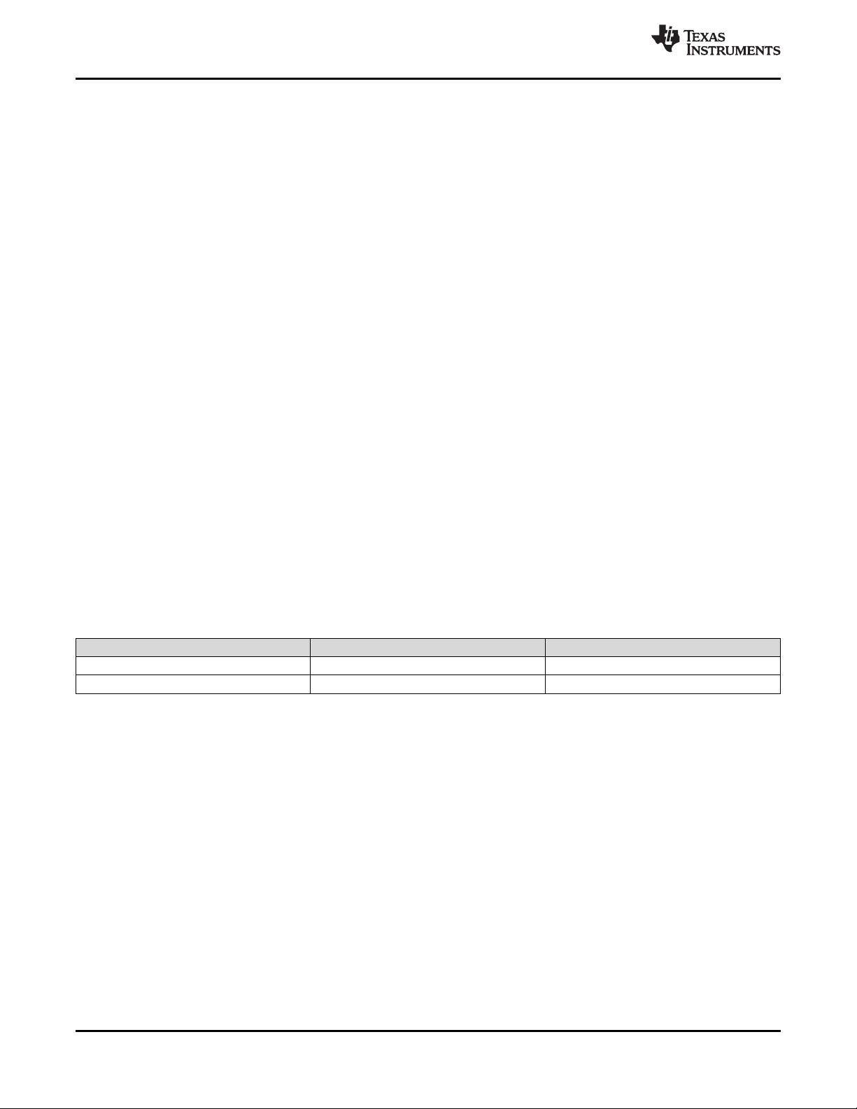
Program/Data Storage
Serial Interfaces
Connectivity
I2C x5
UART x10
McSPI x4
DCAN x2
McASP x8
System
Spinlock
(2x Arm
Cortex–A15)
DSP1 C66x
Co-Processors
PCIe SS x2
Mailbox x13
GPIO x8
Timers x16
WDT
MediaLB /
MOST150
GMAC AVB
up to 2.5MiB
RAM w/ ECC
SATA
(NAND/NOR/
Async)
MMC / SD x4
2x 32b
DMM
2x VCP
HD ATL
(Dual-Core
SGX544 3D)
BB2D
320 2D)
VIP1
QSPI
3x USB 2.0
Dual Mode FS/HS
1x w/ PHY
2x w/ ULPI
EDMA
SDMA
2x EVE
Analytic
Processors
2x MMU
VPE
PWM SS x3
intro_001
KBDHDQ
1x USB 3.0
FS/HS/SS
Dual Mode w/PHY
GPMC / ELM
DDR2/3(L) w/ ECC
(1)
EMIF x2
256KiB
ROM
OCMC
DRA77x / DRA76x
(GC
GPU
MPU
DSP2 C66x
Co-Processors
(Dual Cortex–M4)
IPU1
(Dual Cortex–M4)
IPU2
IVA HD
1080p Video
Co-Processor
Radio Accelerators
High-Speed Interconnect
Copyright © 2016, Texas Instruments Incorporated
MCAN-FD x1
ISS
ISP CAL_B
WDR & Mesh LDC
VIP2
CAL CSI2 x2
Display Subsystem
LCD2
LCD1
1xGFX / 3xVID
Blend / Scale
HDMI 1.4a
LCD3
Secure Boot
Debug
Security
TEE
(HS devices)
www.ti.com
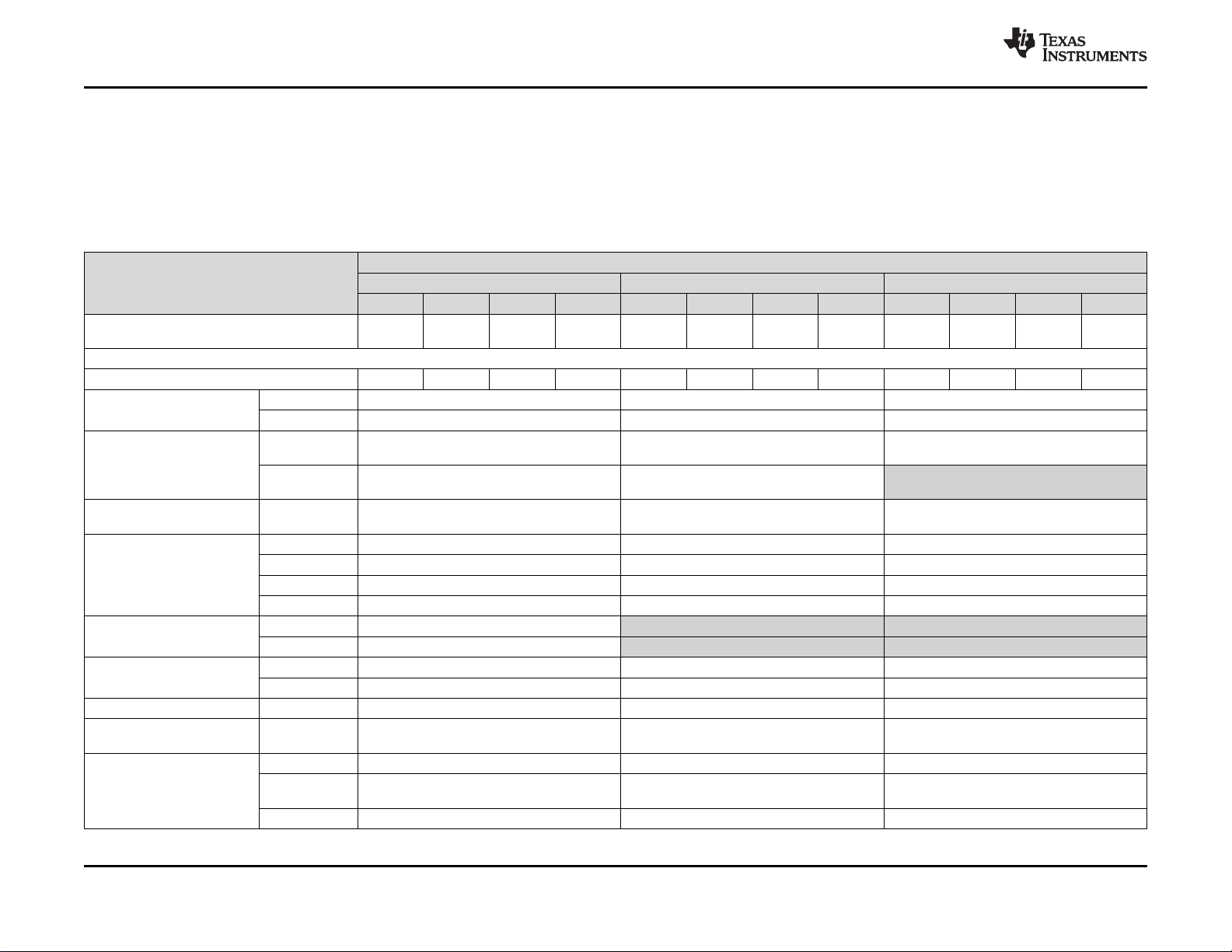
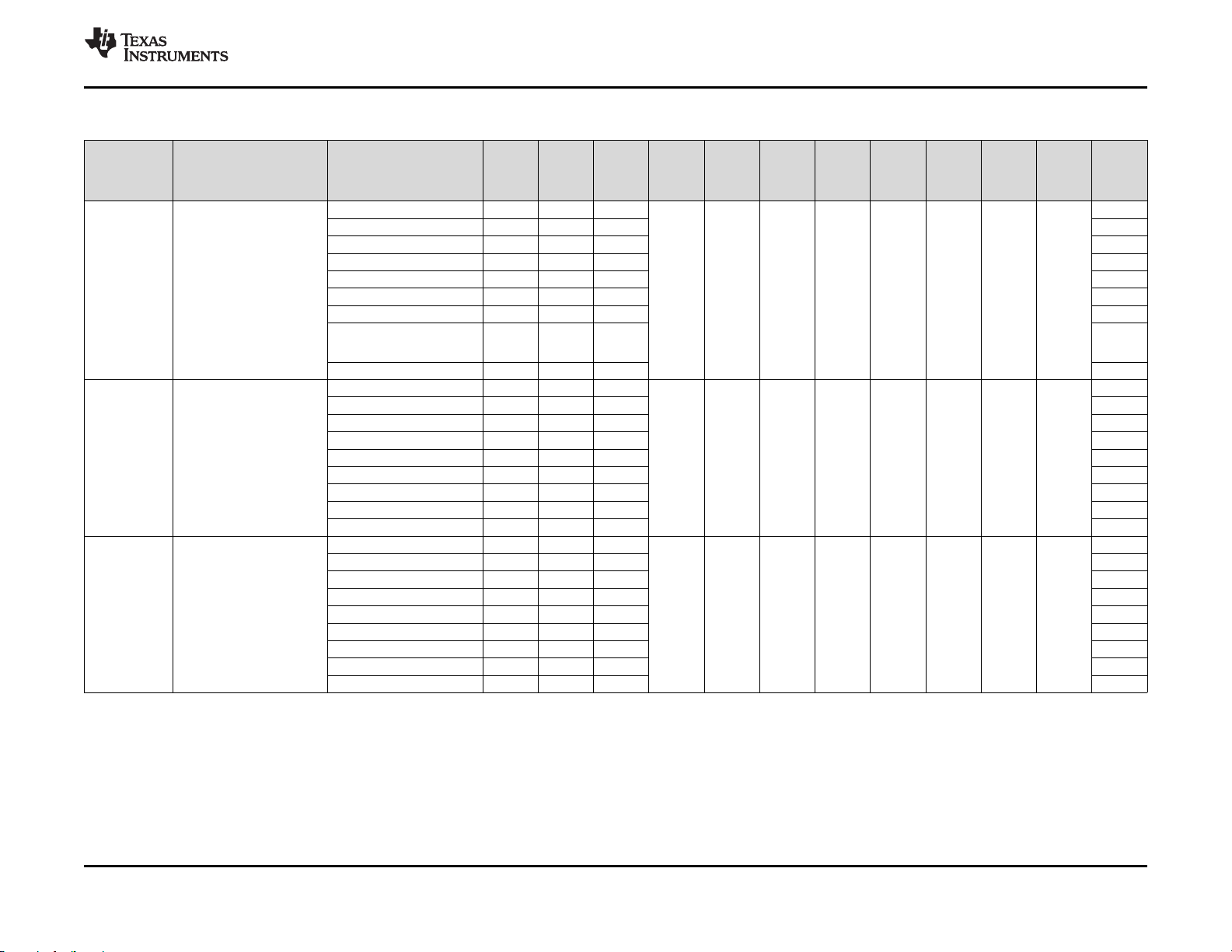
1.4 Functional Block Diagram
Figure 1-1 is functional block diagram for the device.
DRA77P, DRA76P
SPRS993E –MARCH 2017–REVISED DECEMBER 2018
(1) ECC is only available on EMIF1.
Figure 1-1. DRA77xP, DRA76xP Block Diagram
Submit Documentation Feedback
Product Folder Links: DRA77P DRA76P
Device OverviewCopyright © 2017–2018, Texas Instruments Incorporated
3
DRA77P, DRA76P
SPRS993E –MARCH 2017–REVISED DECEMBER 2018
www.ti.com
Table of Contents
1 Device Overview ......................................... 1
1.1 Features .............................................. 1
1.2 Applications........................................... 2
1.3 Description............................................ 2
1.4 Functional Block Diagram ........................... 3
2 Revision History ......................................... 5
3 Device Comparison ..................................... 6
3.1 Device Comparison Table............................ 6
3.2 Related Products.................................... 10
4 Terminal Configuration and Functions ............ 11
4.1 Pin Diagram ......................................... 11
4.2 Pin Attributes ........................................ 11
4.3 Signal Descriptions.................................. 82
4.4 Pin Multiplexing .................................... 124
4.5 Connections for Unused Pins...................... 143
5 Specifications ......................................... 144
5.1 Absolute Maximum Ratings
5.2 ESD Ratings ....................................... 146
5.3 Power-On Hours (POH)
5.4 Recommended Operating Conditions ............. 147
5.5 Operating Performance Points..................... 150
5.6 Power Consumption Summary .................... 173
5.7 Electrical Characteristics........................... 174
5.8 VPP Specifications for One-Time Programmable
(OTP) eFuses...................................... 182
5.9 Thermal Resistance Characteristics ............... 183
5.10 Timing Requirements and Switching
Characteristics ..................................... 185
(1)
..................... 145
(2)
......................... 146
6 Detailed Description.................................. 348
6.1 Description......................................... 348
6.2 Functional Block Diagram ......................... 348
6.3 MPU................................................ 350
6.4 DSP Subsystem ................................... 353
6.5 ISS ................................................. 357
6.6 IVA ................................................. 357
6.7 EVE ................................................ 358
6.8 IPU................................................. 359
6.9 VPE ................................................ 360
6.10 GPU................................................ 362
6.11 ATL Overview...................................... 362
6.12 Memory Subsystem................................ 364
6.13 Interprocessor Communication .................... 367
6.14 Interrupt Controller................................. 368
6.15 EDMA .............................................. 369
6.16 Peripherals......................................... 370
6.17 On-Chip Debug .................................... 386
7 Applications, Implementation, and Layout ...... 390
7.1 Introduction ........................................ 390
7.2 Power Optimizations............................... 391
7.3 Core Power Domains .............................. 405
7.4 Single-Ended Interfaces ........................... 417
7.5 Differential Interfaces .............................. 419
7.6 DDR2/DDR3 Board Design and Layout
Guidelines.......................................... 442
8 Device and Documentation Support.............. 477
8.1 Device Nomenclature .............................. 477
8.2 Tools and Software ................................ 479
8.3 Documentation Support............................ 480
8.4 Receiving Notification of Documentation Updates. 480
8.5 Related Links ...................................... 480
8.6 Community Resources............................. 481
8.7 Trademarks ........................................ 481
8.8 Electrostatic Discharge Caution ................... 481
8.9 Export Control Notice .............................. 481
8.10 Glossary............................................ 481
9 Mechanical Packaging and Orderable
Information............................................. 482
9.1 Mechanical Data ................................... 482
4
Table of Contents Copyright © 2017–2018, Texas Instruments Incorporated
Submit Documentation Feedback
Product Folder Links: DRA77P DRA76P
DRA77P, DRA76P
www.ti.com
SPRS993E –MARCH 2017–REVISED DECEMBER 2018
2 Revision History
Changes from March 17, 2018 to December 15, 2018 (from D Revision (March 2018) to E Revision) Page
• Added clarification notes regarding X5777x part number to Table 3-1, Device Comparison............................... 6
• Updated porz, resetn and rstoutn signal descriptions in Table 4-28 PRCM Signal Descriptions. ...................... 117
• Added table note for maximum valid input voltage on an IO pin to Section 5.1, Absolute Maximum Rating Over
Junction Temperature Range .................................................................................................... 145
• Updated Section 5.3, Power-On Hours (POH)................................................................................. 146
• Added clarification note regarding TSHUT feature. .......................................................................... 150
• Added definition for MPU OPP_LOW in Voltage Domains Operating Performance Points and Supported OPP vs
Max Frequency tables............................................................................................................. 152
• Added Ivpp specification in Table 5-14, Recommended Operating Conditions for OTP eFuse Programming ....... 182
• Updated Section 5.8.3, Impact to Your Hardware Warranty................................................................. 183
• Updated Section 5.10.3, Power Supply Sequences .......................................................................... 187
• Updated system clock names in Section 5.10.4, Clock Specifications ..................................................... 195
• Updated manual mode and timing tables for DSS, GMAC-RGMII, and MMC2 ........................................... 231
• Added missing balls in Table 5-71, McSPI3/4 IOSETs ...................................................................... 274
• Updated phase polarity in all QSPI timing figures............................................................................. 277
• Removed references to OpenGL in Section 6.10, GPU...................................................................... 362
• Updated Section 7.3.5, Power Supply Mapping ............................................................................... 410
• Added new Section 7.3.7, Loss of Input Power Event........................................................................ 411
• Added clarification notes regarding X5777x part number in Table 8-1, Nomenclature Description .................... 478
Submit Documentation Feedback
Product Folder Links: DRA77P DRA76P
Revision HistoryCopyright © 2017–2018, Texas Instruments Incorporated
5
DRA77P, DRA76P
SPRS993E –MARCH 2017–REVISED DECEMBER 2018
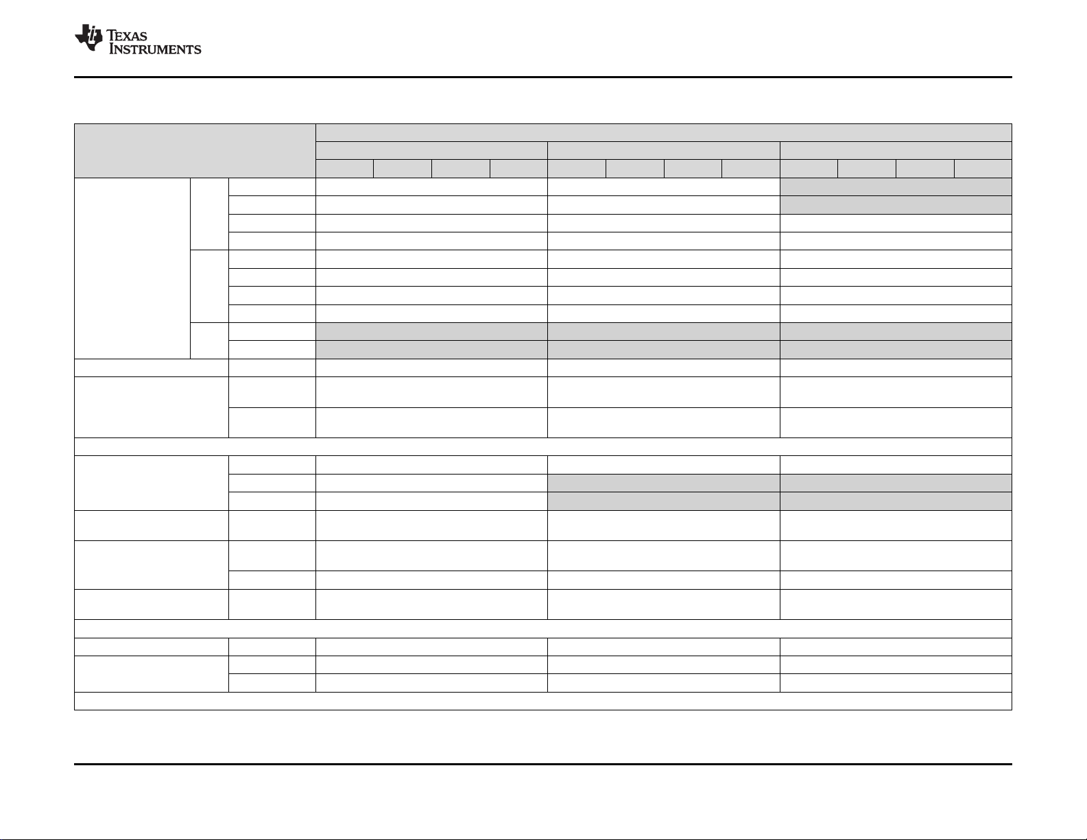
3 Device Comparison
3.1 Device Comparison Table
Table 3-1 shows a comparison between devices, highlighting the differences.
www.ti.com
Table 3-1. Device Comparison
(8)
Features Device
Jacinto 6 Plus EX Jacinto 6 Plus EP Jacinto 6 Plus
DRA777P DRA776P DRA775P DRA774P DRA773P DRA772P DRA771P DRA770P DRA767P DRA766P DRA765P DRA764P
CTRL_WKUP_STD_FUSE_DIE_ID_2[31:24]
Base PN register bitfield value
(7)(8)
104
(0x68)
102
(0x66)
101
(0x65)
100
(0x64)99(0x63)98(0x62)97(0x61)96(0x60)87(0x57)86(0x56)85(0x55)84(0x54)
Processors/ Accelerators
Speed Grades S P L J S P L J S P L J
Dual Arm Cortex-A15
Microprocessor Subsystem
C66x VLIW DSP DSP1
MPU core 0 Yes Yes Yes
MPU core 1 Yes Yes Yes
Yes Yes Yes
(with L1D ECC)
DSP2
Yes Yes No
(with L1D ECC)
BitBLT 2D Hardware
BB2D Yes Yes Yes
Acceleration Engine
Display Subsystem VOUT1 Yes
VOUT2 Yes
VOUT3 Yes
(1)
(1)
(1)
Yes
Yes
Yes
(1)
(1)
(1)
Yes
Yes
Yes
(1)
(1)
(1)
HDMI Yes Yes Yes
Embedded Vision Engine EVE1 Yes No No
EVE2 Yes No No
Dual Arm Cortex-M4 Image
Processing Unit
IPU1 Yes Yes Yes
IPU2 Yes Yes Yes
Image Video Accelarator IVA Yes Yes Yes
SGX544 Dual-Core 3D
GPU Yes Yes Yes
Graphics Processing Unit
Imaging Subsystem (ISS) ISP Optional
WDR & Mesh
(6)
LDC
Optional
CAL_B Optional
(2)
(2)
(2)
Optional
Optional
Optional
(2)
(2)
(2)
Optional
Optional
Optional
(2)
(2)
(2)
6
Copyright © 2017–2018, Texas Instruments IncorporatedDevice Comparison
Submit Documentation Feedback
Product Folder Links: DRA77P DRA76P
www.ti.com
DRA77P, DRA76P
SPRS993E –MARCH 2017–REVISED DECEMBER 2018
Table 3-1. Device Comparison
Features Device
Jacinto 6 Plus EX Jacinto 6 Plus EP Jacinto 6 Plus
DRA777P DRA776P DRA775P DRA774P DRA773P DRA772P DRA771P DRA770P DRA767P DRA766P DRA765P DRA764P
Video Input Port VIP1 vin1a Yes Yes No
vin1b Yes Yes No
vin2a Yes Yes Yes
vin2b Yes Yes Yes
VIP2 vin3a Yes Yes Yes
vin3b Yes Yes Yes
vin4a Yes Yes Yes
vin4b Yes Yes Yes
VIP3 vin5a No No No
vin6a No No No
Video Processing Engine VPE Yes Yes Yes
Camera Adaptation Layer
(CAL) Camera Serial
Interface 2 (CSI2)
Program/Data Storage
On-Chip Shared Memory OCMC_RAM1 512 KB 512 KB 512 KB
General-Purpose Memory
Controller
DDR2/DDR3/DDR3L Memory
Controller
Dynamic Memory Manager
(DMM)
Radio Support
Audio Tracking Logic (ATL) ATL Yes Yes Yes
Viterbi Coprocessor (VCP) VCP1 Yes Yes Yes
Peripherals
(4)
CSI2_0
(CLK + 4 Data)
CSI2_1
(CLK + 2 Data)
OCMC_RAM2 1MB No No
OCMC_RAM3 1MB No No
GPMC Yes Yes Yes
EMIF1 up to 2GB
(with optional R-mod-W ECC)
EMIF2 up to 2GB up to 2GB up to 2GB
DMM Yes Yes Yes
VCP2 Yes Yes Yes
Yes Yes Yes
Yes Yes Yes
(8)
(continued)
(with optional R-mod-W ECC)
up to 2GB
up to 2GB
Copyright © 2017–2018, Texas Instruments Incorporated Device Comparison
Submit Documentation Feedback
Product Folder Links: DRA77P DRA76P
7
DRA77P, DRA76P
SPRS993E –MARCH 2017–REVISED DECEMBER 2018
www.ti.com
Table 3-1. Device Comparison
(8)
(continued)
Features Device
Jacinto 6 Plus EX Jacinto 6 Plus EP Jacinto 6 Plus
DRA777P DRA776P DRA775P DRA774P DRA773P DRA772P DRA771P DRA770P DRA767P DRA766P DRA765P DRA764P
Controller Area Network
Interface (CAN)
(5)
DCAN1
(5)
DCAN2
MCAN with
(5)
FD
Yes Yes Yes
Yes Yes Yes
Yes Yes Yes
Enhanced DMA EDMA Yes Yes Yes
System DMA DMA_SYSTEM Yes Yes Yes
Ethernet Subsystem
(Ethernet SS)
GMAC_SW[0] MII, RMII, or RGMII MII, RMII, or RGMII MII, RMII, or RGMII
GMAC_SW[1] MII, RMII, or RGMII MII, RMII, or RGMII MII, RMII, or RGMII
General-Purpose I/O GPIO Up to 247 Up to 247 Up to 247
Inter-Integrated Circuit
I2C 5 5 5
Interface
System Mailbox Module MAILBOX 13 13 13
Media Local Bus Subsystem MLB 4096 Fs 4096 Fs 4096 Fs
Multi-Channel Audio Serial
Port
McASP1 16 serializers 16 serializers 16 serializers
McASP2 16 serializers 16 serializers 16 serializers
McASP3 4 serializers 4 serializers 4 serializers
McASP4 4 serializers 4 serializers 4 serializers
McASP5 4 serializers 4 serializers 4 serializers
McASP6 4 serializers 4 serializers 4 serializers
McASP7 4 serializers 4 serializers 4 serializers
McASP8 4 serializers 4 serializers 4 serializers
MultiMedia Card/Secure
Digital/Secure Digital Input
Output Interface
(MMC/SD/SDIO)
MMC1 1x UHSI 4b 1x UHSI 4b 1x UHSI 4b
MMC2 1x eMMC™ 8b 1x eMMC 8b 1x eMMC 8b
MMC3 1x SDIO 8b 1x SDIO 8b 1x SDIO 8b
MMC4 1x SDIO 4b 1x SDIO 4b 1x SDIO 4b
PCI Express 3.0 Port with
Integrated PHY
PCIe_SS1 Yes Yes Yes (Single-lane mode)
PCIe_SS2 Yes Yes No
SATA SATA Yes Yes Yes
Real-Time Clock RTCSS No No No
Programmable Real-Time
PRU-ICSS No No No
Unit Subsystem and Industrial
Communication Subsystem
8
Copyright © 2017–2018, Texas Instruments IncorporatedDevice Comparison
Submit Documentation Feedback
Product Folder Links: DRA77P DRA76P
www.ti.com
DRA77P, DRA76P
SPRS993E –MARCH 2017–REVISED DECEMBER 2018
Table 3-1. Device Comparison
Features Device
Jacinto 6 Plus EX Jacinto 6 Plus EP Jacinto 6 Plus
DRA777P DRA776P DRA775P DRA774P DRA773P DRA772P DRA771P DRA770P DRA767P DRA766P DRA765P DRA764P
Multichannel Serial Peripheral
Interface
HDQ1W HDQ1W Yes Yes Yes
Quad SPI QSPI Yes Yes Yes
Spinlock Module SPINLOCK Yes Yes Yes
Keyboard Controller KBD Yes Yes Yes
Timers, General-Purpose TIMER 16 16 16
Timer, Watchdog WATCHDOG
Pulse-Width Modulation
Subsystem
Universal Asynchronous
Receiver/Transmitter
Universal Serial Bus
(USB3.0)
Universal Serial Bus
(USB2.0)
(1) DSS clock jitter can be improved by providing an external clock source (via inputs vin1a_clk, vin1b_clk) or from internal SATA or PCIe PLLs.
(2) Device supports ISS as an optional feature if the part number is designated with the “I” option.
(3) USB4 will not be supported on some pin-compatible roadmap devices. USB3 will be mapped to these balls instead. Pin compatibility can be maintained in the future by either not using
USB4, or via software change to use USB4 on this device, but USB3 on these balls in the future.
(4) In the Unified L3 memory map, there is maximum of 2GB of SDRAM space which is available to all L3 initiators including MPU (MPU, GPU, DSP, IVA, DMA, etc). Typically this space is
interleaved across both EMIFs to optimize memory performance. If a system populates > 2GB of physical memory, that additional addressable space can be accessed only by the MPU
McSPI 4 4 4
TIMER
PWMSS1 Yes Yes Yes
PWMSS2 Yes Yes Yes
PWMSS3 Yes Yes Yes
UART 10 10 10
USB1
(SuperSpeed,
Dual-RoleDevice [DRD])
USB2
(HighSpeed,
Dual-RoleDevice [DRD],
with embedded
HS PHY)
USB3
(HighSpeed,
OTG2.0, with
ULPI)
USB4
(HighSpeed,
OTG2.0, with
ULPI)
Yes Yes Yes
Yes Yes Yes
Yes Yes Yes
Yes Yes Yes
Yes Yes Yes
(8)
(continued)
(3)
Copyright © 2017–2018, Texas Instruments Incorporated Device Comparison
Submit Documentation Feedback
Product Folder Links: DRA77P DRA76P
9

DRA77P, DRA76P
SPRS993E –MARCH 2017–REVISED DECEMBER 2018
via the Arm V7 Large Physical Address Extensions (LPAE).
(5) DCAN1 has one pin mux option that can optionally be used for MCAN functionality. DCAN2 has two pin mux options, one of which can be optionally used for MCAN functionality.
(6) Wide Dynamic Range and Lens Distortion Correction.
(7) For more details about the CTRL_WKUP_STD_FUSE_DIE_ID_2 register and Base PN bitfield, see the Jacinto 6 Plus Technical Reference Manual.
(8) X577Px is the base part number for the superset device. Software should constrain the features used to match the intended production device. The Base PN register bitfield value is 0x69.
www.ti.com
3.2 Related Products
Automotive Processors
DRAx Infotainment SoCs The "Jacinto 6" family of infotainment processors (DRA7xx), paired with robust software and ecosystem offering bring
unprecedented feature-rich, in-vehicle infotainment, instrument cluster and telematics features to the next generation automobiles.
10
Copyright © 2017–2018, Texas Instruments IncorporatedDevice Comparison
Submit Documentation Feedback
Product Folder Links: DRA77P DRA76P
ACD_001
www.ti.com
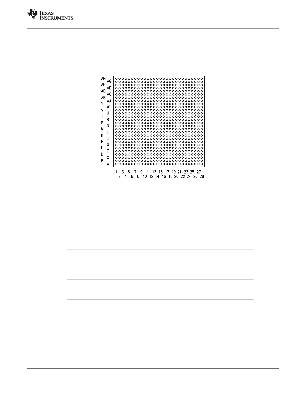
4 Terminal Configuration and Functions
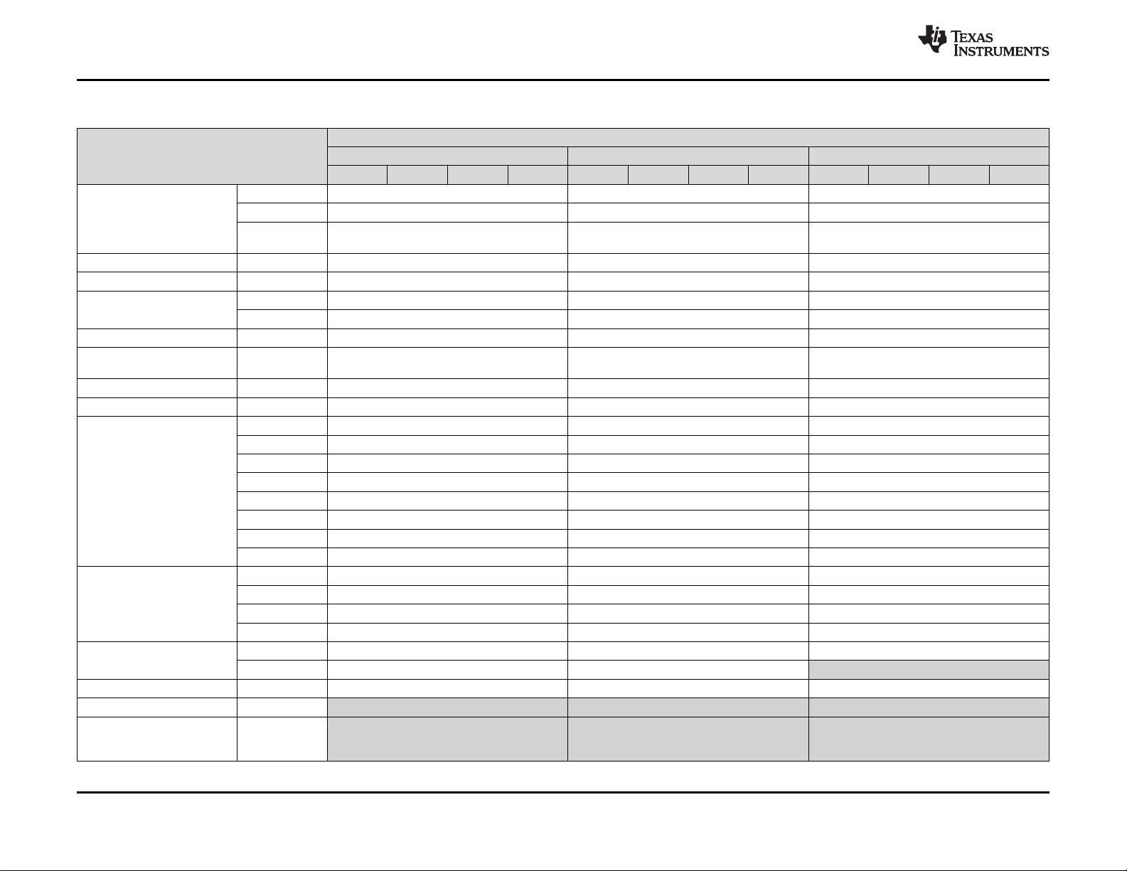
4.1 Pin Diagram
Figure 4-1 shows the ball locations for the 784 plastic ball grid array (PBGA) package and are used in
conjunction with Table 4-1 through Table 4-32 to locate signal names and ball grid numbers.
DRA77P, DRA76P
SPRS993E –MARCH 2017–REVISED DECEMBER 2018
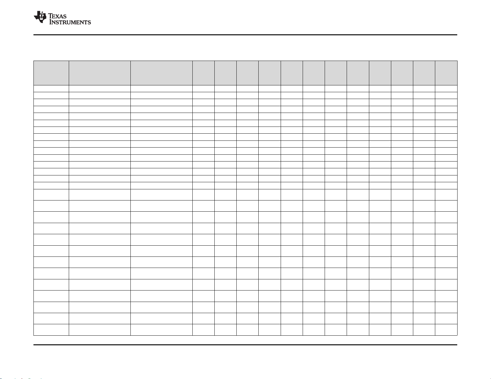
4.2 Pin Attributes
Table 4-1 describes the terminal characteristics and the signals multiplexed on each ball. The following list
describes the table column headers:
1. BALL NUMBER: Ball number(s) on the bottom side associated with each signal on the bottom.
2. BALL NAME: Mechanical name from package device (name is taken from muxmode 0).
3. SIGNAL NAME: Names of signals multiplexed on each ball (also notice that the name of the ball is the
signal name in muxmode 0).
Table 4-1 does not take into account the subsystem multiplexing signals. Subsystem
multiplexing signals are described in Section 4.3, Signal Descriptions.
In the Driver off mode, the buffer is configured in high-impedance.
4. 76xP: This column shows if the functionality is applicable for DRA76xP devices. Note that the Pin
Attributes table presents the functionality of DRA77xP device. An empty box means "Yes".
5. MUXMODE: Multiplexing mode number:
a. MUXMODE 0 is the primary mode; this means that when MUXMODE = 0 is set, the function
mapped on the pin corresponds to the name of the pin. The primary muxmode is not necessarily
the default muxmode.
Figure 4-1. ACD S-PBGA-N784 Package (Bottom View)
NOTE
NOTE
Submit Documentation Feedback
Product Folder Links: DRA77P DRA76P
Terminal Configuration and FunctionsCopyright © 2017–2018, Texas Instruments Incorporated
11

DRA77P, DRA76P
SPRS993E –MARCH 2017–REVISED DECEMBER 2018
The default mode is the mode at the release of the reset; also see the RESET REL.
MUXMODE column.
b. MUXMODE 1 through 15 are possible muxmodes for alternate functions. On each pin, some
muxmodes are effectively used for alternate functions, while some muxmodes are not used. Only
MUXMODE values which correspond to defined functions should be used.
c. An empty box means Not Applicable.
6. TYPE: Signal type and direction:
– I = Input
– O = Output
– IO = Input or Output
– D = Open drain
– DS = Differential Signaling
– A = Analog
– PWR = Power
– GND = Ground
– CAP = LDO Capacitor
7. BALL RESET STATE: The state of the terminal at power-on reset:
– drive 0 (OFF): The buffer drives VOL(pulldown or pullup resistor not activated)
– drive 1 (OFF): The buffer drives VOH(pulldown or pullup resistor not activated)
– OFF: High-impedance
– PD: High-impedance with an active pulldown resistor
– PU: High-impedance with an active pullup resistor
– An empty box means Not Applicable
8. BALL RESET REL. STATE: The state of the terminal at the deactivation of the rstoutn signal (also
mapped to the PRCM SYS_WARM_OUT_RST signal)
– drive 0 (OFF): The buffer drives VOL(pulldown or pullup resistor not activated)
– drive clk (OFF): The buffer drives a toggling clock (pulldown or pullup resistor not activated)
– drive 1 (OFF): The buffer drives VOH(pulldown or pullup resistor not activated)
– OFF: High-impedance
– PD: High-impedance with an active pulldown resistor
– PU: High-impedance with an active pullup resistor
– An empty box means Not Applicable
www.ti.com
NOTE
12
NOTE
For more information on the CORE_PWRON_RET_RST reset signal and its reset sources,
see the Power Reset and Clock Management / PRCM Reset Management Functional
Description section of the Device TRM.
9. BALL RESET REL. MUXMODE: This muxmode is automatically configured at the release of the
rstoutn signal (also mapped to the PRCM SYS_WARM_OUT_RST signal).
An empty box means Not Applicable.
10. IO VOLTAGE VALUE: This column describes the IO voltage value (the corresponding power supply).
An empty box means Not Applicable.
11. POWER: The voltage supply that powers the terminal IO buffers.
An empty box means Not Applicable.
12. HYS: Indicates if the input buffer is with hysteresis:
– Yes: With hysteresis
– No: Without hysteresis
Terminal Configuration and Functions Copyright © 2017–2018, Texas Instruments Incorporated
Submit Documentation Feedback
Product Folder Links: DRA77P DRA76P
www.ti.com
13. BUFFER TYPE: Drive strength of the associated output buffer.
14. PULLUP / PULLDOWN TYPE: Denotes the presence of an internal pullup or pulldown resistor.
15. DSIS: The deselected input state (DSIS) indicates the state driven on the peripheral input (logic "0" or
DRA77P, DRA76P
SPRS993E –MARCH 2017–REVISED DECEMBER 2018
– An empty box: Not Applicable
NOTE
For more information, see the hysteresis values in Section 5.7, Electrical Characteristics.
An empty box means Not Applicable.
NOTE
For programmable buffer strength:
– The default value is given in Table 4-1.
– A note describes all possible values according to the selected muxmode.
Pullup and pulldown resistors can be enabled or disabled via software.
– PU: Internal pullup
– PD: Internal pulldown
– PU/PD: Internal pullup and pulldown
– PUx/PDy: Programmable internal pullup and pulldown
– PDy: Programmable internal pulldown
– An empty box means No pull
logic "1") when the peripheral pin function is not selected by any of the PINCNTLx registers.
– 0: Logic 0 driven on the peripheral's input signal port.
– 1: Logic 1 driven on the peripheral's input signal port.
– Blank: Pin state driven on the peripheral's input signal port.
NOTE
Configuring two pins to the same input signal is not supported as it can yield unexpected
results. This can be easily prevented with the proper software configuration (Hi-Z mode is not
an input signal).
NOTE
When a pad is set into a multiplexing mode which is not defined by pin multiplexing, that
pad’s behavior is undefined. This should be avoided.
CAUTION
Peripherals exposed in Pin Attributes Table and Pin Multiplexing Table
represent functionality of a DRA77xP device. Not all exposed peripherals are
supported on DRA7xx devices. For peripherals supported on DRA7xx family of
products please refer to Table 3-1, Device Comparison.
Submit Documentation Feedback
Product Folder Links: DRA77P DRA76P
Terminal Configuration and FunctionsCopyright © 2017–2018, Texas Instruments Incorporated
13

DRA77P, DRA76P
SPRS993E –MARCH 2017–REVISED DECEMBER 2018
Some of the DDR1 and DDR2 signals have an additional state change at the release of porz.
The state that the signals change to at the release of porz is as follows:
drive 0 (OFF) for: ddr1_csn0, ddr1_ck, ddr1_nck, ddr1_nck, ddr1_casn, ddr1_rasn,
ddr1_wen, ddr1_ba[2:0], ddr1_a[15:0], ddr2_csn0, ddr2_ck, ddr2_nck, ddr2_casn, ddr2_rasn,
ddr2_wen, ddr2_ba[2:0], ddr2_a[15:0].
OFF for: ddr1_ecc_d[7:0], ddr1_dqm[3:0], ddr1_dqm_ecc, ddr1_dqs[3:0], ddr1_dqsn[3:0],
ddr1_dqs_ecc, ddr1_dqsn_ecc, ddr1_d[31:0], ddr2_dqm[3:0], ddr2_dqs[3:0], ddr2_dqsn[3:0],
ddr2_d[31:0].
www.ti.com
NOTE
14
Terminal Configuration and Functions Copyright © 2017–2018, Texas Instruments Incorporated
Submit Documentation Feedback
Product Folder Links: DRA77P DRA76P
www.ti.com
DRA77P, DRA76P
SPRS993E –MARCH 2017–REVISED DECEMBER 2018
BALL
RESET
STATE [7]
(1)
RESET
STATE [8]
BALL
REL.
BALL
RESET
REL.
MUXMODE
[9]
I/O
VOLTAGE
VALUE [10]
POWER
[11]
HYS [12]
BUFFER
TYPE [13]
CSI2
CSI2
CSI2
CSI2
CSI2
CSI2
CSI2
CSI2
CSI2
CSI2
CSI2
CSI2
CSI2
Table 4-1. Pin Attributes
BALL NUMBER [1] BALL NAME [2] SIGNAL NAME [3] 76x [4]
J11 cap_vbbldo_dspeve cap_vbbldo_dspeve CAP
U13 cap_vbbldo_gpu cap_vbbldo_gpu CAP
R19 cap_vbbldo_iva cap_vbbldo_iva CAP
J19 cap_vbbldo_mpu cap_vbbldo_mpu CAP
H11 cap_vddram_core1 cap_vddram_core1 CAP
J17 cap_vddram_core2 cap_vddram_core2 CAP
U15 cap_vddram_core3 cap_vddram_core3 CAP
R17 cap_vddram_core4 cap_vddram_core4 CAP
Y16 cap_vddram_core5 cap_vddram_core5 CAP
G10 cap_vddram_dspeve1 cap_vddram_dspeve1 CAP
H10 cap_vddram_dspeve2 cap_vddram_dspeve2 CAP
T16 cap_vddram_gpu cap_vddram_gpu CAP
R20 cap_vddram_iva cap_vddram_iva CAP
J16 cap_vddram_mpu1 cap_vddram_mpu1 CAP
J21 cap_vddram_mpu2 cap_vddram_mpu2 CAP
AD17 csi2_0_dx0 csi2_0_dx0 0 I 1.8 vdda_csi Yes LVCMOS
AF16 csi2_0_dx1 csi2_0_dx1 0 I 1.8 vdda_csi Yes LVCMOS
AF19 csi2_0_dx2 csi2_0_dx2 0 I 1.8 vdda_csi Yes LVCMOS
AE15 csi2_0_dx3 csi2_0_dx3 0 I 1.8 vdda_csi Yes LVCMOS
AE19 csi2_0_dx4 csi2_0_dx4 0 I 1.8 vdda_csi Yes LVCMOS
AD18 csi2_0_dy0 csi2_0_dy0 0 I 1.8 vdda_csi Yes LVCMOS
AF17 csi2_0_dy1 csi2_0_dy1 0 I 1.8 vdda_csi Yes LVCMOS
AF20 csi2_0_dy2 csi2_0_dy2 0 I 1.8 vdda_csi Yes LVCMOS
AE16 csi2_0_dy3 csi2_0_dy3 0 I 1.8 vdda_csi Yes LVCMOS
AE18 csi2_0_dy4 csi2_0_dy4 0 I 1.8 vdda_csi Yes LVCMOS
AC13 csi2_1_dx0 csi2_1_dx0 0 I 1.8 vdda_csi Yes LVCMOS
AD15 csi2_1_dx1 csi2_1_dx1 0 I 1.8 vdda_csi Yes LVCMOS
AC16 csi2_1_dx2 csi2_1_dx2 0 I 1.8 vdda_csi Yes LVCMOS
MUXMODE
[5]
TYPE [6]
PULL
UP/DOWN
TYPE [14]
PU/PD
PU/PD
PU/PD
PU/PD
PU/PD
PU/PD
PU/PD
PU/PD
PU/PD
PU/PD
PU/PD
PU/PD
PU/PD
DSIS [15]
Copyright © 2017–2018, Texas Instruments Incorporated Terminal Configuration and Functions
Submit Documentation Feedback
Product Folder Links: DRA77P DRA76P
15
DRA77P, DRA76P
SPRS993E –MARCH 2017–REVISED DECEMBER 2018
www.ti.com
Table 4-1. Pin Attributes
BALL NUMBER [1] BALL NAME [2] SIGNAL NAME [3] 76x [4]
AC14 csi2_1_dy0 csi2_1_dy0 0 I 1.8 vdda_csi Yes LVCMOS
AD14 csi2_1_dy1 csi2_1_dy1 0 I 1.8 vdda_csi Yes LVCMOS
AC17 csi2_1_dy2 csi2_1_dy2 0 I 1.8 vdda_csi Yes LVCMOS
D19 dcan1_rx dcan1_rx
E19 dcan1_tx dcan1_tx
AG19 ddr1_casn ddr1_casn 0 O PD drive 1
AG24 ddr1_ck ddr1_ck 0 O PD drive clk
AH23 ddr1_cke ddr1_cke 0 O PD drive 0
T27 ddr1_dqm_ecc ddr1_dqm_ecc No 0 O PD PD 1.35/1.5/1.8 vdds_ddr1 No LVCMOS
U28 ddr1_dqsn_ecc ddr1_dqsn_ecc No 0 IO PU PU 1.35/1.5/1.8 vdds_ddr1 LVCMOS
U27 ddr1_dqs_ecc ddr1_dqs_ecc No 0 IO PD PD 1.35/1.5/1.8 vdds_ddr1 LVCMOS
AH24 ddr1_nck ddr1_nck 0 O PD drive clk
AH20 ddr1_rasn ddr1_rasn 0 O PD drive 1
AF23 ddr1_rst ddr1_rst 0 O PD drive 0
AG22 ddr1_wen ddr1_wen 0 O PD drive 1
T25 ddr2_casn ddr2_casn 0 O PD drive 1
mcan_rx
uart8_txd 2 O
mmc2_sdwp 3 I 0
sata1_led 4 O
hdmi1_cec 6 IO
gpio1_15 14 IO
Driver off 15 I
mcan_tx
uart8_rxd 2 I 1
mmc2_sdcd 3 I 1
hdmi1_hpd 6 I
gpio1_14 14 IO
Driver off 15 I
MUXMODE
0 IO PU PU 15 1.8/3.3 vddshv3 Yes Dual
0 IO PU PU 15 1.8/3.3 vddshv3 Yes Dual
TYPE [6]
[5]
(1)
(continued)
BALL
RESET
STATE [7]
(OFF)
(OFF)
(OFF)
(OFF)
(OFF)
(OFF)
(OFF)
(OFF)
BALL
RESET
REL.
STATE [8]
BALL
RESET
REL.
MUXMODE
[9]
I/O
VOLTAGE
VALUE [10]
1.35/1.5/1.8 vdds_ddr1 No LVCMOS
1.35/1.5/1.8 vdds_ddr1 No LVCMOS
1.35/1.5/1.8 vdds_ddr1 No LVCMOS
1.35/1.5/1.8 vdds_ddr1 No LVCMOS
1.35/1.5/1.8 vdds_ddr1 No LVCMOS
1.35/1.5/1.8 vdds_ddr1 No LVCMOS
1.35/1.5/1.8 vdds_ddr1 No LVCMOS
1.35/1.5/1.8 vdds_ddr2 No LVCMOS
POWER
[11]
HYS [12]
BUFFER
TYPE [13]
CSI2
CSI2
CSI2
Voltage
LVCMOS
Voltage
LVCMOS
DDR
DDR
DDR
DDR
DDR
DDR
DDR
DDR
DDR
DDR
DDR
PULL
UP/DOWN
TYPE [14]
PU/PD
PU/PD
PU/PD
PU/PD
PU/PD
Pux/PDy
Pux/PDy
Pux/PDy
Pux/PDy
Pux/PDy
Pux/PDy
Pux/PDy
Pux/PDy
Pux/PDy
Pux/PDy
Pux/PDy
DSIS [15]
16
Copyright © 2017–2018, Texas Instruments IncorporatedTerminal Configuration and Functions
Submit Documentation Feedback
Product Folder Links: DRA77P DRA76P

www.ti.com
DRA77P, DRA76P
SPRS993E –MARCH 2017–REVISED DECEMBER 2018
Table 4-1. Pin Attributes
BALL NUMBER [1] BALL NAME [2] SIGNAL NAME [3] 76x [4]
R28 ddr2_ck ddr2_ck 0 O PD drive clk
R25 ddr2_cke ddr2_cke 0 O PD drive 0
R27 ddr2_nck ddr2_nck 0 O PD drive clk
R26 ddr2_rasn ddr2_rasn 0 O PD drive 1
N25 ddr2_rst ddr2_rst 0 O PD drive 0
T24 ddr2_wen ddr2_wen 0 O PD drive 1
AE22 ddr1_a0 ddr1_a0 0 O PD drive 1
AD20 ddr1_a1 ddr1_a1 0 O PD drive 1
AE21 ddr1_a2 ddr1_a2 0 O PD drive 1
AD22 ddr1_a3 ddr1_a3 0 O PD drive 1
AE23 ddr1_a4 ddr1_a4 0 O PD drive 1
AH22 ddr1_a5 ddr1_a5 0 O PD drive 1
AD24 ddr1_a6 ddr1_a6 0 O PD drive 1
AC22 ddr1_a7 ddr1_a7 0 O PD drive 1
AG23 ddr1_a8 ddr1_a8 0 O PD drive 1
AF24 ddr1_a9 ddr1_a9 0 O PD drive 1
AD21 ddr1_a10 ddr1_a10 0 O PD drive 1
AE24 ddr1_a11 ddr1_a11 0 O PD drive 1
AG21 ddr1_a12 ddr1_a12 0 O PD drive 1
AF21 ddr1_a13 ddr1_a13 0 O PD drive 1
AC23 ddr1_a14 ddr1_a14 0 O PD drive 1
AG20 ddr1_a15 ddr1_a15 0 O PD drive 1
AE20 ddr1_ba0 ddr1_ba0 0 O PD drive 1
MUXMODE
[5]
TYPE [6]
(1)
(continued)
BALL
RESET
STATE [7]
(OFF)
(OFF)
(OFF)
(OFF)
(OFF)
(OFF)
(OFF)
(OFF)
(OFF)
(OFF)
(OFF)
(OFF)
(OFF)
(OFF)
(OFF)
(OFF)
(OFF)
(OFF)
(OFF)
(OFF)
(OFF)
(OFF)
(OFF)
BALL
RESET
REL.
STATE [8]
BALL
RESET
REL.
MUXMODE
[9]
I/O
VOLTAGE
VALUE [10]
1.35/1.5/1.8 vdds_ddr2 No LVCMOS
1.35/1.5/1.8 vdds_ddr2 No LVCMOS
1.35/1.5/1.8 vdds_ddr2 No LVCMOS
1.35/1.5/1.8 vdds_ddr2 No LVCMOS
1.35/1.5/1.8 vdds_ddr2 No LVCMOS
1.35/1.5/1.8 vdds_ddr2 No LVCMOS
1.35/1.5/1.8 vdds_ddr1 No LVCMOS
1.35/1.5/1.8 vdds_ddr1 No LVCMOS
1.35/1.5/1.8 vdds_ddr1 No LVCMOS
1.35/1.5/1.8 vdds_ddr1 No LVCMOS
1.35/1.5/1.8 vdds_ddr1 No LVCMOS
1.35/1.5/1.8 vdds_ddr1 No LVCMOS
1.35/1.5/1.8 vdds_ddr1 No LVCMOS
1.35/1.5/1.8 vdds_ddr1 No LVCMOS
1.35/1.5/1.8 vdds_ddr1 No LVCMOS
1.35/1.5/1.8 vdds_ddr1 No LVCMOS
1.35/1.5/1.8 vdds_ddr1 No LVCMOS
1.35/1.5/1.8 vdds_ddr1 No LVCMOS
1.35/1.5/1.8 vdds_ddr1 No LVCMOS
1.35/1.5/1.8 vdds_ddr1 No LVCMOS
1.35/1.5/1.8 vdds_ddr1 No LVCMOS
1.35/1.5/1.8 vdds_ddr1 No LVCMOS
1.35/1.5/1.8 vdds_ddr1 No LVCMOS
POWER
[11]
HYS [12]
BUFFER
TYPE [13]
DDR
DDR
DDR
DDR
DDR
DDR
DDR
DDR
DDR
DDR
DDR
DDR
DDR
DDR
DDR
DDR
DDR
DDR
DDR
DDR
DDR
DDR
DDR
PULL
UP/DOWN
TYPE [14]
Pux/PDy
Pux/PDy
Pux/PDy
Pux/PDy
Pux/PDy
Pux/PDy
Pux/PDy
Pux/PDy
Pux/PDy
Pux/PDy
Pux/PDy
Pux/PDy
Pux/PDy
Pux/PDy
Pux/PDy
Pux/PDy
Pux/PDy
Pux/PDy
Pux/PDy
Pux/PDy
Pux/PDy
Pux/PDy
Pux/PDy
DSIS [15]
Copyright © 2017–2018, Texas Instruments Incorporated Terminal Configuration and Functions
Submit Documentation Feedback
Product Folder Links: DRA77P DRA76P
17
DRA77P, DRA76P
SPRS993E –MARCH 2017–REVISED DECEMBER 2018
www.ti.com
Table 4-1. Pin Attributes
BALL NUMBER [1] BALL NAME [2] SIGNAL NAME [3] 76x [4]
AC21 ddr1_ba1 ddr1_ba1 0 O PD drive 1
AH21 ddr1_ba2 ddr1_ba2 0 O PD drive 1
AD23 ddr1_csn0 ddr1_csn0 0 O PD drive 1
AE26 ddr1_d0 ddr1_d0 0 IO PD PD 1.35/1.5/1.8 vdds_ddr1 No LVCMOS
AE27 ddr1_d1 ddr1_d1 0 IO PD PD 1.35/1.5/1.8 vdds_ddr1 No LVCMOS
AF28 ddr1_d2 ddr1_d2 0 IO PD PD 1.35/1.5/1.8 vdds_ddr1 No LVCMOS
AH26 ddr1_d3 ddr1_d3 0 IO PD PD 1.35/1.5/1.8 vdds_ddr1 No LVCMOS
AF25 ddr1_d4 ddr1_d4 0 IO PD PD 1.35/1.5/1.8 vdds_ddr1 No LVCMOS
AG27 ddr1_d5 ddr1_d5 0 IO PD PD 1.35/1.5/1.8 vdds_ddr1 No LVCMOS
AF27 ddr1_d6 ddr1_d6 0 IO PD PD 1.35/1.5/1.8 vdds_ddr1 No LVCMOS
AF26 ddr1_d7 ddr1_d7 0 IO PD PD 1.35/1.5/1.8 vdds_ddr1 No LVCMOS
AB24 ddr1_d8 ddr1_d8 0 IO PD PD 1.35/1.5/1.8 vdds_ddr1 No LVCMOS
AD27 ddr1_d9 ddr1_d9 0 IO PD PD 1.35/1.5/1.8 vdds_ddr1 No LVCMOS
AE28 ddr1_d10 ddr1_d10 0 IO PD PD 1.35/1.5/1.8 vdds_ddr1 No LVCMOS
AD28 ddr1_d11 ddr1_d11 0 IO PD PD 1.35/1.5/1.8 vdds_ddr1 No LVCMOS
AD26 ddr1_d12 ddr1_d12 0 IO PD PD 1.35/1.5/1.8 vdds_ddr1 No LVCMOS
AE25 ddr1_d13 ddr1_d13 0 IO PD PD 1.35/1.5/1.8 vdds_ddr1 No LVCMOS
AD25 ddr1_d14 ddr1_d14 0 IO PD PD 1.35/1.5/1.8 vdds_ddr1 No LVCMOS
AC26 ddr1_d15 ddr1_d15 0 IO PD PD 1.35/1.5/1.8 vdds_ddr1 No LVCMOS
AA25 ddr1_d16 ddr1_d16 0 IO PD PD 1.35/1.5/1.8 vdds_ddr1 No LVCMOS
AB25 ddr1_d17 ddr1_d17 0 IO PD PD 1.35/1.5/1.8 vdds_ddr1 No LVCMOS
AA26 ddr1_d18 ddr1_d18 0 IO PD PD 1.35/1.5/1.8 vdds_ddr1 No LVCMOS
AA28 ddr1_d19 ddr1_d19 0 IO PD PD 1.35/1.5/1.8 vdds_ddr1 No LVCMOS
MUXMODE
[5]
TYPE [6]
(1)
(continued)
BALL
RESET
STATE [7]
(OFF)
(OFF)
(OFF)
BALL
RESET
REL.
STATE [8]
BALL
RESET
REL.
MUXMODE
[9]
I/O
VOLTAGE
VALUE [10]
1.35/1.5/1.8 vdds_ddr1 No LVCMOS
1.35/1.5/1.8 vdds_ddr1 No LVCMOS
1.35/1.5/1.8 vdds_ddr1 No LVCMOS
POWER
[11]
HYS [12]
BUFFER
TYPE [13]
DDR
DDR
DDR
DDR
DDR
DDR
DDR
DDR
DDR
DDR
DDR
DDR
DDR
DDR
DDR
DDR
DDR
DDR
DDR
DDR
DDR
DDR
DDR
PULL
UP/DOWN
TYPE [14]
Pux/PDy
Pux/PDy
Pux/PDy
Pux/PDy
Pux/PDy
Pux/PDy
Pux/PDy
Pux/PDy
Pux/PDy
Pux/PDy
Pux/PDy
Pux/PDy
Pux/PDy
Pux/PDy
Pux/PDy
Pux/PDy
Pux/PDy
Pux/PDy
Pux/PDy
Pux/PDy
Pux/PDy
Pux/PDy
Pux/PDy
DSIS [15]
18
Copyright © 2017–2018, Texas Instruments IncorporatedTerminal Configuration and Functions
Submit Documentation Feedback
Product Folder Links: DRA77P DRA76P

www.ti.com
DRA77P, DRA76P
SPRS993E –MARCH 2017–REVISED DECEMBER 2018
Table 4-1. Pin Attributes
BALL NUMBER [1] BALL NAME [2] SIGNAL NAME [3] 76x [4]
AA27 ddr1_d20 ddr1_d20 0 IO PD PD 1.35/1.5/1.8 vdds_ddr1 No LVCMOS
AA24 ddr1_d21 ddr1_d21 0 IO PD PD 1.35/1.5/1.8 vdds_ddr1 No LVCMOS
AC25 ddr1_d22 ddr1_d22 0 IO PD PD 1.35/1.5/1.8 vdds_ddr1 No LVCMOS
Y26 ddr1_d23 ddr1_d23 0 IO PD PD 1.35/1.5/1.8 vdds_ddr1 No LVCMOS
W26 ddr1_d24 ddr1_d24 0 IO PD PD 1.35/1.5/1.8 vdds_ddr1 No LVCMOS
AB23 ddr1_d25 ddr1_d25 0 IO PD PD 1.35/1.5/1.8 vdds_ddr1 No LVCMOS
V24 ddr1_d26 ddr1_d26 0 IO PD PD 1.35/1.5/1.8 vdds_ddr1 No LVCMOS
Y24 ddr1_d27 ddr1_d27 0 IO PD PD 1.35/1.5/1.8 vdds_ddr1 No LVCMOS
W25 ddr1_d28 ddr1_d28 0 IO PD PD 1.35/1.5/1.8 vdds_ddr1 No LVCMOS
Y25 ddr1_d29 ddr1_d29 0 IO PD PD 1.35/1.5/1.8 vdds_ddr1 No LVCMOS
W24 ddr1_d30 ddr1_d30 0 IO PD PD 1.35/1.5/1.8 vdds_ddr1 No LVCMOS
Y28 ddr1_d31 ddr1_d31 0 IO PD PD 1.35/1.5/1.8 vdds_ddr1 No LVCMOS
AG26 ddr1_dqm0 ddr1_dqm0 0 O PD PD 1.35/1.5/1.8 vdds_ddr1 No LVCMOS
AC24 ddr1_dqm1 ddr1_dqm1 0 O PD PD 1.35/1.5/1.8 vdds_ddr1 No LVCMOS
AB26 ddr1_dqm2 ddr1_dqm2 0 O PD PD 1.35/1.5/1.8 vdds_ddr1 No LVCMOS
Y27 ddr1_dqm3 ddr1_dqm3 0 O PD PD 1.35/1.5/1.8 vdds_ddr1 No LVCMOS
AH25 ddr1_dqs0 ddr1_dqs0 0 IO PD PD 1.35/1.5/1.8 vdds_ddr1 LVCMOS
AC27 ddr1_dqs1 ddr1_dqs1 0 IO PD PD 1.35/1.5/1.8 vdds_ddr1 LVCMOS
AB27 ddr1_dqs2 ddr1_dqs2 0 IO PD PD 1.35/1.5/1.8 vdds_ddr1 LVCMOS
W28 ddr1_dqs3 ddr1_dqs3 0 IO PD PD 1.35/1.5/1.8 vdds_ddr1 LVCMOS
AG25 ddr1_dqsn0 ddr1_dqsn0 0 IO PU PU 1.35/1.5/1.8 vdds_ddr1 LVCMOS
AC28 ddr1_dqsn1 ddr1_dqsn1 0 IO PU PU 1.35/1.5/1.8 vdds_ddr1 LVCMOS
AB28 ddr1_dqsn2 ddr1_dqsn2 0 IO PU PU 1.35/1.5/1.8 vdds_ddr1 LVCMOS
MUXMODE
[5]
TYPE [6]
(1)
(continued)
BALL
RESET
STATE [7]
BALL
RESET
REL.
STATE [8]
BALL
RESET
REL.
MUXMODE
[9]
I/O
VOLTAGE
VALUE [10]
POWER
[11]
HYS [12]
BUFFER
TYPE [13]
DDR
DDR
DDR
DDR
DDR
DDR
DDR
DDR
DDR
DDR
DDR
DDR
DDR
DDR
DDR
DDR
DDR
DDR
DDR
DDR
DDR
DDR
DDR
PULL
UP/DOWN
TYPE [14]
Pux/PDy
Pux/PDy
Pux/PDy
Pux/PDy
Pux/PDy
Pux/PDy
Pux/PDy
Pux/PDy
Pux/PDy
Pux/PDy
Pux/PDy
Pux/PDy
Pux/PDy
Pux/PDy
Pux/PDy
Pux/PDy
Pux/PDy
Pux/PDy
Pux/PDy
Pux/PDy
Pux/PDy
Pux/PDy
Pux/PDy
DSIS [15]
Copyright © 2017–2018, Texas Instruments Incorporated Terminal Configuration and Functions
Submit Documentation Feedback
Product Folder Links: DRA77P DRA76P
19

DRA77P, DRA76P
SPRS993E –MARCH 2017–REVISED DECEMBER 2018
www.ti.com
Table 4-1. Pin Attributes
BALL NUMBER [1] BALL NAME [2] SIGNAL NAME [3] 76x [4]
W27 ddr1_dqsn3 ddr1_dqsn3 0 IO PU PU 1.35/1.5/1.8 vdds_ddr1 LVCMOS
U25 ddr1_ecc_d0 ddr1_ecc_d0 No 0 IO PD PD 1.35/1.5/1.8 vdds_ddr1 No LVCMOS
U26 ddr1_ecc_d1 ddr1_ecc_d1 No 0 IO PD PD 1.35/1.5/1.8 vdds_ddr1 No LVCMOS
V25 ddr1_ecc_d2 ddr1_ecc_d2 No 0 IO PD PD 1.35/1.5/1.8 vdds_ddr1 No LVCMOS
V26 ddr1_ecc_d3 ddr1_ecc_d3 No 0 IO PD PD 1.35/1.5/1.8 vdds_ddr1 No LVCMOS
V27 ddr1_ecc_d4 ddr1_ecc_d4 No 0 IO PD PD 1.35/1.5/1.8 vdds_ddr1 No LVCMOS
T28 ddr1_ecc_d5 ddr1_ecc_d5 No 0 IO PD PD 1.35/1.5/1.8 vdds_ddr1 No LVCMOS
T26 ddr1_ecc_d6 ddr1_ecc_d6 No 0 IO PD PD 1.35/1.5/1.8 vdds_ddr1 No LVCMOS
V28 ddr1_ecc_d7 ddr1_ecc_d7 No 0 IO PD PD 1.35/1.5/1.8 vdds_ddr1 No LVCMOS
AF22 ddr1_odt0 ddr1_odt0 0 O PD drive 0
AB22 ddr1_vref0 ddr1_vref0 0 PWR OFF OFF 1.35/1.5/1.8 vdds_ddr1 No LVCMOS
P25 ddr2_a0 ddr2_a0 0 O PD drive 1
P26 ddr2_a1 ddr2_a1 0 O PD drive 1
P28 ddr2_a2 ddr2_a2 0 O PD drive 1
P27 ddr2_a3 ddr2_a3 0 O PD drive 1
P24 ddr2_a4 ddr2_a4 0 O PD drive 1
P23 ddr2_a5 ddr2_a5 0 O PD drive 1
N26 ddr2_a6 ddr2_a6 0 O PD drive 1
M25 ddr2_a7 ddr2_a7 0 O PD drive 1
N28 ddr2_a8 ddr2_a8 0 O PD drive 1
M27 ddr2_a9 ddr2_a9 0 O PD drive 1
L25 ddr2_a10 ddr2_a10 0 O PD drive 1
N27 ddr2_a11 ddr2_a11 0 O PD drive 1
MUXMODE
[5]
TYPE [6]
(1)
(continued)
BALL
RESET
STATE [7]
(OFF)
(OFF)
(OFF)
(OFF)
(OFF)
(OFF)
(OFF)
(OFF)
(OFF)
(OFF)
(OFF)
(OFF)
(OFF)
BALL
RESET
REL.
STATE [8]
BALL
RESET
REL.
MUXMODE
[9]
I/O
VOLTAGE
VALUE [10]
1.35/1.5/1.8 vdds_ddr1 No LVCMOS
1.35/1.5/1.8 vdds_ddr2 No LVCMOS
1.35/1.5/1.8 vdds_ddr2 No LVCMOS
1.35/1.5/1.8 vdds_ddr2 No LVCMOS
1.35/1.5/1.8 vdds_ddr2 No LVCMOS
1.35/1.5/1.8 vdds_ddr2 No LVCMOS
1.35/1.5/1.8 vdds_ddr2 No LVCMOS
1.35/1.5/1.8 vdds_ddr2 No LVCMOS
1.35/1.5/1.8 vdds_ddr2 No LVCMOS
1.35/1.5/1.8 vdds_ddr2 No LVCMOS
1.35/1.5/1.8 vdds_ddr2 No LVCMOS
1.35/1.5/1.8 vdds_ddr2 No LVCMOS
1.35/1.5/1.8 vdds_ddr2 No LVCMOS
POWER
[11]
HYS [12]
BUFFER
TYPE [13]
DDR
DDR
DDR
DDR
DDR
DDR
DDR
DDR
DDR
DDR
DDR
DDR
DDR
DDR
DDR
DDR
DDR
DDR
DDR
DDR
DDR
DDR
DDR
PULL
UP/DOWN
TYPE [14]
Pux/PDy
Pux/PDy
Pux/PDy
Pux/PDy
Pux/PDy
Pux/PDy
Pux/PDy
Pux/PDy
Pux/PDy
Pux/PDy
Pux/PDy
Pux/PDy
Pux/PDy
Pux/PDy
Pux/PDy
Pux/PDy
Pux/PDy
Pux/PDy
Pux/PDy
Pux/PDy
Pux/PDy
Pux/PDy
DSIS [15]
20
Copyright © 2017–2018, Texas Instruments IncorporatedTerminal Configuration and Functions
Submit Documentation Feedback
Product Folder Links: DRA77P DRA76P
www.ti.com
DRA77P, DRA76P
SPRS993E –MARCH 2017–REVISED DECEMBER 2018
Table 4-1. Pin Attributes
BALL NUMBER [1] BALL NAME [2] SIGNAL NAME [3] 76x [4]
M28 ddr2_a12 ddr2_a12 0 O PD drive 1
R24 ddr2_a13 ddr2_a13 0 O PD drive 1
N24 ddr2_a14 ddr2_a14 0 O PD drive 1
R23 ddr2_a15 ddr2_a15 0 O PD drive 1
L24 ddr2_ba0 ddr2_ba0 0 O PD drive 1
U24 ddr2_ba1 ddr2_ba1 0 O PD drive 1
M24 ddr2_ba2 ddr2_ba2 0 O PD drive 1
M26 ddr2_csn0 ddr2_csn0 0 O PD drive 1
C28 ddr2_d0 ddr2_d0 0 IO PU PU 1.35/1.5/1.8 vdds_ddr2 No LVCMOS
A26 ddr2_d1 ddr2_d1 0 IO PU PU 1.35/1.5/1.8 vdds_ddr2 No LVCMOS
E24 ddr2_d2 ddr2_d2 0 IO PU PU 1.35/1.5/1.8 vdds_ddr2 No LVCMOS
D25 ddr2_d3 ddr2_d3 0 IO PU PU 1.35/1.5/1.8 vdds_ddr2 No LVCMOS
D26 ddr2_d4 ddr2_d4 0 IO PU PU 1.35/1.5/1.8 vdds_ddr2 No LVCMOS
B27 ddr2_d5 ddr2_d5 0 IO PU PU 1.35/1.5/1.8 vdds_ddr2 No LVCMOS
B26 ddr2_d6 ddr2_d6 0 IO PU PU 1.35/1.5/1.8 vdds_ddr2 No LVCMOS
C26 ddr2_d7 ddr2_d7 0 IO PU PU 1.35/1.5/1.8 vdds_ddr2 No LVCMOS
F26 ddr2_d8 ddr2_d8 0 IO PU PU 1.35/1.5/1.8 vdds_ddr2 No LVCMOS
E25 ddr2_d9 ddr2_d9 0 IO PU PU 1.35/1.5/1.8 vdds_ddr2 No LVCMOS
E26 ddr2_d10 ddr2_d10 0 IO PU PU 1.35/1.5/1.8 vdds_ddr2 No LVCMOS
G27 ddr2_d11 ddr2_d11 0 IO PU PU 1.35/1.5/1.8 vdds_ddr2 No LVCMOS
E28 ddr2_d12 ddr2_d12 0 IO PU PU 1.35/1.5/1.8 vdds_ddr2 No LVCMOS
G26 ddr2_d13 ddr2_d13 0 IO PU PU 1.35/1.5/1.8 vdds_ddr2 No LVCMOS
G28 ddr2_d14 ddr2_d14 0 IO PU PU 1.35/1.5/1.8 vdds_ddr2 No LVCMOS
MUXMODE
[5]
TYPE [6]
(1)
(continued)
BALL
RESET
STATE [7]
(OFF)
(OFF)
(OFF)
(OFF)
(OFF)
(OFF)
(OFF)
(OFF)
BALL
RESET
REL.
STATE [8]
BALL
RESET
REL.
MUXMODE
[9]
I/O
VOLTAGE
VALUE [10]
1.35/1.5/1.8 vdds_ddr2 No LVCMOS
1.35/1.5/1.8 vdds_ddr2 No LVCMOS
1.35/1.5/1.8 vdds_ddr2 No LVCMOS
1.35/1.5/1.8 vdds_ddr2 No LVCMOS
1.35/1.5/1.8 vdds_ddr2 No LVCMOS
1.35/1.5/1.8 vdds_ddr2 No LVCMOS
1.35/1.5/1.8 vdds_ddr2 No LVCMOS
1.35/1.5/1.8 vdds_ddr2 No LVCMOS
POWER
[11]
HYS [12]
BUFFER
TYPE [13]
DDR
DDR
DDR
DDR
DDR
DDR
DDR
DDR
DDR
DDR
DDR
DDR
DDR
DDR
DDR
DDR
DDR
DDR
DDR
DDR
DDR
DDR
DDR
PULL
UP/DOWN
TYPE [14]
Pux/PDy
Pux/PDy
Pux/PDy
Pux/PDy
Pux/PDy
Pux/PDy
Pux/PDy
Pux/PDy
Pux/PDy
Pux/PDy
Pux/PDy
Pux/PDy
Pux/PDy
Pux/PDy
Pux/PDy
Pux/PDy
Pux/PDy
Pux/PDy
Pux/PDy
Pux/PDy
Pux/PDy
Pux/PDy
Pux/PDy
DSIS [15]
Copyright © 2017–2018, Texas Instruments Incorporated Terminal Configuration and Functions
Submit Documentation Feedback
Product Folder Links: DRA77P DRA76P
21

DRA77P, DRA76P
SPRS993E –MARCH 2017–REVISED DECEMBER 2018
www.ti.com
Table 4-1. Pin Attributes
BALL NUMBER [1] BALL NAME [2] SIGNAL NAME [3] 76x [4]
F25 ddr2_d15 ddr2_d15 0 IO PU PU 1.35/1.5/1.8 vdds_ddr2 No LVCMOS
G25 ddr2_d16 ddr2_d16 0 IO PU PU 1.35/1.5/1.8 vdds_ddr2 No LVCMOS
G24 ddr2_d17 ddr2_d17 0 IO PU PU 1.35/1.5/1.8 vdds_ddr2 No LVCMOS
F23 ddr2_d18 ddr2_d18 0 IO PU PU 1.35/1.5/1.8 vdds_ddr2 No LVCMOS
F24 ddr2_d19 ddr2_d19 0 IO PU PU 1.35/1.5/1.8 vdds_ddr2 No LVCMOS
H28 ddr2_d20 ddr2_d20 0 IO PU PU 1.35/1.5/1.8 vdds_ddr2 No LVCMOS
H25 ddr2_d21 ddr2_d21 0 IO PU PU 1.35/1.5/1.8 vdds_ddr2 No LVCMOS
H27 ddr2_d22 ddr2_d22 0 IO PU PU 1.35/1.5/1.8 vdds_ddr2 No LVCMOS
H26 ddr2_d23 ddr2_d23 0 IO PU PU 1.35/1.5/1.8 vdds_ddr2 No LVCMOS
K27 ddr2_d24 ddr2_d24 0 IO PU PU 1.35/1.5/1.8 vdds_ddr2 No LVCMOS
K26 ddr2_d25 ddr2_d25 0 IO PU PU 1.35/1.5/1.8 vdds_ddr2 No LVCMOS
J25 ddr2_d26 ddr2_d26 0 IO PU PU 1.35/1.5/1.8 vdds_ddr2 No LVCMOS
K28 ddr2_d27 ddr2_d27 0 IO PU PU 1.35/1.5/1.8 vdds_ddr2 No LVCMOS
H24 ddr2_d28 ddr2_d28 0 IO PU PU 1.35/1.5/1.8 vdds_ddr2 No LVCMOS
J24 ddr2_d29 ddr2_d29 0 IO PU PU 1.35/1.5/1.8 vdds_ddr2 No LVCMOS
K24 ddr2_d30 ddr2_d30 0 IO PU PU 1.35/1.5/1.8 vdds_ddr2 No LVCMOS
L26 ddr2_d31 ddr2_d31 0 IO PU PU 1.35/1.5/1.8 vdds_ddr2 No LVCMOS
C27 ddr2_dqm0 ddr2_dqm0 0 O PU PU 1.35/1.5/1.8 vdds_ddr2 No LVCMOS
E27 ddr2_dqm1 ddr2_dqm1 0 O PU PU 1.35/1.5/1.8 vdds_ddr2 No LVCMOS
G23 ddr2_dqm2 ddr2_dqm2 0 O PU PU 1.35/1.5/1.8 vdds_ddr2 No LVCMOS
J26 ddr2_dqm3 ddr2_dqm3 0 O PU PU 1.35/1.5/1.8 vdds_ddr2 No LVCMOS
D28 ddr2_dqs0 ddr2_dqs0 0 IO PD PD 1.35/1.5/1.8 vdds_ddr2 LVCMOS
F27 ddr2_dqs1 ddr2_dqs1 0 IO PD PD 1.35/1.5/1.8 vdds_ddr2 LVCMOS
MUXMODE
[5]
TYPE [6]
(1)
(continued)
BALL
RESET
STATE [7]
BALL
RESET
REL.
STATE [8]
BALL
RESET
REL.
MUXMODE
[9]
I/O
VOLTAGE
VALUE [10]
POWER
[11]
HYS [12]
BUFFER
TYPE [13]
DDR
DDR
DDR
DDR
DDR
DDR
DDR
DDR
DDR
DDR
DDR
DDR
DDR
DDR
DDR
DDR
DDR
DDR
DDR
DDR
DDR
DDR
DDR
PULL
UP/DOWN
TYPE [14]
Pux/PDy
Pux/PDy
Pux/PDy
Pux/PDy
Pux/PDy
Pux/PDy
Pux/PDy
Pux/PDy
Pux/PDy
Pux/PDy
Pux/PDy
Pux/PDy
Pux/PDy
Pux/PDy
Pux/PDy
Pux/PDy
Pux/PDy
Pux/PDy
Pux/PDy
Pux/PDy
Pux/PDy
Pux/PDy
Pux/PDy
DSIS [15]
22
Copyright © 2017–2018, Texas Instruments IncorporatedTerminal Configuration and Functions
Submit Documentation Feedback
Product Folder Links: DRA77P DRA76P
www.ti.com
DRA77P, DRA76P
SPRS993E –MARCH 2017–REVISED DECEMBER 2018
Table 4-1. Pin Attributes
BALL NUMBER [1] BALL NAME [2] SIGNAL NAME [3] 76x [4]
J27 ddr2_dqs2 ddr2_dqs2 0 IO PD PD 1.35/1.5/1.8 vdds_ddr2 LVCMOS
L28 ddr2_dqs3 ddr2_dqs3 0 IO PD PD 1.35/1.5/1.8 vdds_ddr2 LVCMOS
D27 ddr2_dqsn0 ddr2_dqsn0 0 IO PU PU 1.35/1.5/1.8 vdds_ddr2 LVCMOS
F28 ddr2_dqsn1 ddr2_dqsn1 0 IO PU PU 1.35/1.5/1.8 vdds_ddr2 LVCMOS
J28 ddr2_dqsn2 ddr2_dqsn2 0 IO PU PU 1.35/1.5/1.8 vdds_ddr2 LVCMOS
L27 ddr2_dqsn3 ddr2_dqsn3 0 IO PU PU 1.35/1.5/1.8 vdds_ddr2 LVCMOS
K25 ddr2_odt0 ddr2_odt0 0 O PD drive 0
M22 ddr2_vref0 ddr2_vref0 0 PWR OFF OFF 1.35/1.5/1.8 vdds_ddr2 No LVCMOS
F19 emu0 emu0 0 IO PU PU 0 1.8/3.3 vddshv3 Yes Dual
gpio8_30 14 IO
C23 emu1 emu1 0 IO PU PU 0 1.8/3.3 vddshv3 Yes Dual
gpio8_31 14 IO
AC5 gpio6_10 gpio6_10 0 IO PU PU 15 1.8/3.3 vddshv7 Yes Dual
mdio_mclk 1 O 1
i2c3_sda 2 IO 1
usb3_ulpi_d7 3 IO 0
vin2b_hsync1 4 I
ehrpwm2A 10 O
gpio6_10 14 IO
Driver off 15 I
AB4 gpio6_11 gpio6_11 0 IO PU PU 15 1.8/3.3 vddshv7 Yes Dual
mdio_d 1 IO 1
i2c3_scl 2 IO 1
usb3_ulpi_d6 3 IO 0
vin2b_vsync1 4 I
ehrpwm2B 10 O
gpio6_11 14 IO
Driver off 15 I
MUXMODE
[5]
TYPE [6]
(1)
(continued)
BALL
RESET
STATE [7]
(OFF)
BALL
RESET
REL.
STATE [8]
BALL
RESET
REL.
MUXMODE
[9]
I/O
VOLTAGE
VALUE [10]
1.35/1.5/1.8 vdds_ddr2 No LVCMOS
POWER
[11]
HYS [12]
BUFFER
TYPE [13]
DDR
DDR
DDR
DDR
DDR
DDR
DDR
DDR
Voltage
LVCMOS
Voltage
LVCMOS
Voltage
LVCMOS
Voltage
LVCMOS
PULL
UP/DOWN
TYPE [14]
Pux/PDy
Pux/PDy
Pux/PDy
Pux/PDy
Pux/PDy
Pux/PDy
Pux/PDy
PU/PD
PU/PD
PU/PD
PU/PD
DSIS [15]
Copyright © 2017–2018, Texas Instruments Incorporated Terminal Configuration and Functions
Submit Documentation Feedback
Product Folder Links: DRA77P DRA76P
23

DRA77P, DRA76P
SPRS993E –MARCH 2017–REVISED DECEMBER 2018
www.ti.com
Table 4-1. Pin Attributes
BALL NUMBER [1] BALL NAME [2] SIGNAL NAME [3] 76x [4]
E21 gpio6_14 gpio6_14 0 IO PU PU 15 1.8/3.3 vddshv3 Yes Dual
mcasp1_axr8 1 IO 0
dcan2_tx
mcan_tx
uart10_rxd 3 I 1
vout2_hsync 6 O
vin4a_hsync0 8 I 0
i2c3_sda 9 IO 1
timer1 10 IO
gpio6_14 14 IO
Driver off 15 I
F17 gpio6_15 gpio6_15 0 IO PU PU 15 1.8/3.3 vddshv3 Yes Dual
mcasp1_axr9 1 IO 0
dcan2_rx
mcan_rx
uart10_txd 3 O
vout2_vsync 6 O
vin4a_vsync0 8 I 0
i2c3_scl 9 IO 1
timer2 10 IO
gpio6_15 14 IO
Driver off 15 I
F18 gpio6_16 gpio6_16 0 IO PU PU 15 1.8/3.3 vddshv3 Yes Dual
mcasp1_axr10 1 IO 0
vout2_fld 6 O
vin4a_fld0 8 I 0
clkout1 9 O
timer3 10 IO
gpio6_16 14 IO
Driver off 15 I
MUXMODE
[5]
2 IO
2 IO
TYPE [6]
(1)
(continued)
BALL
RESET
STATE [7]
BALL
RESET
REL.
STATE [8]
BALL
RESET
REL.
MUXMODE
[9]
I/O
VOLTAGE
VALUE [10]
POWER
[11]
HYS [12]
BUFFER
TYPE [13]
Voltage
LVCMOS
Voltage
LVCMOS
Voltage
LVCMOS
PULL
UP/DOWN
TYPE [14]
PU/PD
PU/PD
PU/PD
DSIS [15]
24
Copyright © 2017–2018, Texas Instruments IncorporatedTerminal Configuration and Functions
Submit Documentation Feedback
Product Folder Links: DRA77P DRA76P
www.ti.com
DRA77P, DRA76P
SPRS993E –MARCH 2017–REVISED DECEMBER 2018
Table 4-1. Pin Attributes
BALL NUMBER [1] BALL NAME [2] SIGNAL NAME [3] 76x [4]
P6 gpmc_a0 gpmc_a0 0 O PD PD 15 1.8/3.3 vddshv10 Yes Dual
vin3a_d16 2 I 0
vout3_d16 3 O
vin4a_d0 4 I 0
vin4b_d0 6 I 0
i2c4_scl 7 IO 1
uart5_rxd 8 I 1
gpio7_3
gpmc_a26
gpmc_a16
Driver off 15 I
J6 gpmc_a1 gpmc_a1 0 O PD PD 15 1.8/3.3 vddshv10 Yes Dual
vin3a_d17 2 I 0
vout3_d17 3 O
vin4a_d1 4 I 0
vin4b_d1 6 I 0
i2c4_sda 7 IO 1
uart5_txd 8 O
gpio7_4 14 IO
Driver off 15 I
R4 gpmc_a2 gpmc_a2 0 O PD PD 15 1.8/3.3 vddshv10 Yes Dual
vin3a_d18 2 I 0
vout3_d18 3 O
vin4a_d2 4 I 0
vin4b_d2 6 I 0
uart7_rxd 7 I 1
uart5_ctsn 8 I 1
gpio7_5 14 IO
Driver off 15 I
MUXMODE
[5]
14 IO
TYPE [6]
(1)
(continued)
BALL
RESET
STATE [7]
BALL
RESET
REL.
STATE [8]
BALL
RESET
REL.
MUXMODE
[9]
I/O
VOLTAGE
VALUE [10]
POWER
[11]
HYS [12]
BUFFER
TYPE [13]
Voltage
LVCMOS
Voltage
LVCMOS
Voltage
LVCMOS
PULL
UP/DOWN
TYPE [14]
PU/PD
PU/PD
PU/PD
DSIS [15]
Copyright © 2017–2018, Texas Instruments Incorporated Terminal Configuration and Functions
Submit Documentation Feedback
Product Folder Links: DRA77P DRA76P
25
DRA77P, DRA76P
SPRS993E –MARCH 2017–REVISED DECEMBER 2018
www.ti.com
Table 4-1. Pin Attributes
BALL NUMBER [1] BALL NAME [2] SIGNAL NAME [3] 76x [4]
R5 gpmc_a3 gpmc_a3 0 O PD PD 15 1.8/3.3 vddshv10 Yes Dual
qspi1_cs2 1 O 1
vin3a_d19 2 I 0
vout3_d19 3 O
vin4a_d3 4 I 0
vin4b_d3 6 I 0
uart7_txd 7 O
uart5_rtsn 8 O
gpio7_6 14 IO
Driver off 15 I
M6 gpmc_a4 gpmc_a4 0 O PD PD 15 1.8/3.3 vddshv10 Yes Dual
qspi1_cs3 1 O 1
vin3a_d20 2 I 0
vout3_d20 3 O
vin4a_d4 4 I 0
vin4b_d4 6 I 0
i2c5_scl 7 IO 1
uart6_rxd 8 I 1
gpio1_26 14 IO
Driver off 15 I
K4 gpmc_a5 gpmc_a5 0 O PD PD 15 1.8/3.3 vddshv10 Yes Dual
vin3a_d21 2 I 0
vout3_d21 3 O
vin4a_d5 4 I 0
vin4b_d5 6 I 0
i2c5_sda 7 IO 1
uart6_txd 8 O
gpio1_27 14 IO
Driver off 15 I
MUXMODE
[5]
TYPE [6]
(1)
(continued)
BALL
RESET
STATE [7]
BALL
RESET
REL.
STATE [8]
BALL
RESET
REL.
MUXMODE
[9]
I/O
VOLTAGE
VALUE [10]
POWER
[11]
HYS [12]
BUFFER
TYPE [13]
Voltage
LVCMOS
Voltage
LVCMOS
Voltage
LVCMOS
PULL
UP/DOWN
TYPE [14]
PU/PD
PU/PD
PU/PD
DSIS [15]
26
Copyright © 2017–2018, Texas Instruments IncorporatedTerminal Configuration and Functions
Submit Documentation Feedback
Product Folder Links: DRA77P DRA76P
www.ti.com
DRA77P, DRA76P
SPRS993E –MARCH 2017–REVISED DECEMBER 2018
Table 4-1. Pin Attributes
BALL NUMBER [1] BALL NAME [2] SIGNAL NAME [3] 76x [4]
P5 gpmc_a6 gpmc_a6 0 O PD PD 15 1.8/3.3 vddshv10 Yes Dual
vin3a_d22 2 I 0
vout3_d22 3 O
vin4a_d6 4 I 0
vin4b_d6 6 I 0
uart8_rxd 7 I 1
uart6_ctsn 8 I 1
gpio1_28 14 IO
Driver off 15 I
N6 gpmc_a7 gpmc_a7 0 O PD PD 15 1.8/3.3 vddshv10 Yes Dual
vin3a_d23 2 I 0
vout3_d23 3 O
vin4a_d7 4 I 0
vin4b_d7 6 I 0
uart8_txd 7 O
uart6_rtsn 8 O
gpio1_29 14 IO
Driver off 15 I
N4 gpmc_a8 gpmc_a8 0 O PD PD 15 1.8/3.3 vddshv10 Yes Dual
vin3a_hsync0 2 I 0
vout3_hsync 3 O
vin4b_hsync1 6 I 0
timer12 7 IO
spi4_sclk 8 IO 0
gpio1_30 14 IO
Driver off 15 I
R3 gpmc_a9 gpmc_a9 0 O PD PD 15 1.8/3.3 vddshv10 Yes Dual
vin3a_vsync0 2 I 0
vout3_vsync 3 O
vin4b_vsync1 6 I 0
timer11 7 IO
spi4_d1 8 IO 0
gpio1_31 14 IO
Driver off 15 I
MUXMODE
[5]
TYPE [6]
(1)
(continued)
BALL
RESET
STATE [7]
BALL
RESET
REL.
STATE [8]
BALL
RESET
REL.
MUXMODE
[9]
I/O
VOLTAGE
VALUE [10]
POWER
[11]
HYS [12]
BUFFER
TYPE [13]
Voltage
LVCMOS
Voltage
LVCMOS
Voltage
LVCMOS
Voltage
LVCMOS
PULL
UP/DOWN
TYPE [14]
PU/PD
PU/PD
PU/PD
PU/PD
DSIS [15]
Copyright © 2017–2018, Texas Instruments Incorporated Terminal Configuration and Functions
Submit Documentation Feedback
Product Folder Links: DRA77P DRA76P
27
DRA77P, DRA76P
SPRS993E –MARCH 2017–REVISED DECEMBER 2018
www.ti.com
Table 4-1. Pin Attributes
BALL NUMBER [1] BALL NAME [2] SIGNAL NAME [3] 76x [4]
J5 gpmc_a10 gpmc_a10 0 O PD PD 15 1.8/3.3 vddshv10 Yes Dual
vin3a_de0 2 I 0
vout3_de 3 O
vin4b_clk1 6 I 0
timer10 7 IO
spi4_d0 8 IO 0
gpio2_0 14 IO
Driver off 15 I
K5 gpmc_a11 gpmc_a11 0 O PD PD 15 1.8/3.3 vddshv10 Yes Dual
vin3a_fld0 2 I 0
vout3_fld 3 O
vin4a_fld0 4 I 0
vin4b_de1 6 I 0
timer9 7 IO
spi4_cs0 8 IO 1
gpio2_1 14 IO
Driver off 15 I
P4 gpmc_a12 gpmc_a12 0 O PD PD 15 1.8/3.3 vddshv10 Yes Dual
vin4a_clk0 4 I 0
gpmc_a0 5 O
vin4b_fld1 6 I 0
timer8 7 IO
spi4_cs1 8 IO 1
dma_evt1 9 I 0
gpio2_2 14 IO
Driver off 15 I
R2 gpmc_a13 gpmc_a13 0 O PD PD 15 1.8/3.3 vddshv10 Yes Dual
qspi1_rtclk 1 I 0
vin4a_hsync0 4 I 0
timer7 7 IO
spi4_cs2 8 IO 1
dma_evt2 9 I 0
gpio2_3 14 IO
Driver off 15 I
MUXMODE
[5]
TYPE [6]
(1)
(continued)
BALL
RESET
STATE [7]
BALL
RESET
REL.
STATE [8]
BALL
RESET
REL.
MUXMODE
[9]
I/O
VOLTAGE
VALUE [10]
POWER
[11]
HYS [12]
BUFFER
TYPE [13]
Voltage
LVCMOS
Voltage
LVCMOS
Voltage
LVCMOS
Voltage
LVCMOS
PULL
UP/DOWN
TYPE [14]
PU/PD
PU/PD
PU/PD
PU/PD
DSIS [15]
28
Copyright © 2017–2018, Texas Instruments IncorporatedTerminal Configuration and Functions
Submit Documentation Feedback
Product Folder Links: DRA77P DRA76P
www.ti.com
DRA77P, DRA76P
SPRS993E –MARCH 2017–REVISED DECEMBER 2018
Table 4-1. Pin Attributes
BALL NUMBER [1] BALL NAME [2] SIGNAL NAME [3] 76x [4]
R6 gpmc_a14 gpmc_a14 0 O PD PD 15 1.8/3.3 vddshv10 Yes Dual
qspi1_d3 1 I 0
vin4a_vsync0 4 I 0
timer6 7 IO
spi4_cs3 8 IO 1
gpio2_4 14 IO
Driver off 15 I
T2 gpmc_a15 gpmc_a15 0 O PD PD 15 1.8/3.3 vddshv10 Yes Dual
qspi1_d2 1 I 0
vin4a_d8 4 I 0
timer5 7 IO
gpio2_5 14 IO
Driver off 15 I
U1 gpmc_a16 gpmc_a16 0 O PD PD 15 1.8/3.3 vddshv10 Yes Dual
qspi1_d0 1 IO 0
vin4a_d9 4 I 0
gpio2_6 14 IO
Driver off 15 I
P3 gpmc_a17 gpmc_a17 0 O PD PD 15 1.8/3.3 vddshv10 Yes Dual
qspi1_d1 1 I 0
vin4a_d10 4 I 0
gpio2_7 14 IO
Driver off 15 I
R1 gpmc_a18 gpmc_a18 0 O PD PD 15 1.8/3.3 vddshv10 Yes Dual
qspi1_sclk 1 O
vin4a_d11 4 I 0
gpio2_8 14 IO
Driver off 15 I
H6 gpmc_a19 gpmc_a19 0 O PD PD 15 1.8/3.3 vddshv11 Yes Dual
mmc2_dat4 1 IO 1
gpmc_a13 2 O
vin4a_d12 4 I 0
vin3b_d0 6 I 0
gpio2_9 14 IO
Driver off 15 I
MUXMODE
[5]
TYPE [6]
(1)
(continued)
BALL
RESET
STATE [7]
BALL
RESET
REL.
STATE [8]
BALL
RESET
REL.
MUXMODE
[9]
I/O
VOLTAGE
VALUE [10]
POWER
[11]
HYS [12]
BUFFER
TYPE [13]
Voltage
LVCMOS
Voltage
LVCMOS
Voltage
LVCMOS
Voltage
LVCMOS
Voltage
LVCMOS
Voltage
LVCMOS
PULL
UP/DOWN
TYPE [14]
PU/PD
PU/PD
PU/PD
PU/PD
PU/PD
PU/PD
DSIS [15]
Copyright © 2017–2018, Texas Instruments Incorporated Terminal Configuration and Functions
Submit Documentation Feedback
Product Folder Links: DRA77P DRA76P
29
DRA77P, DRA76P
SPRS993E –MARCH 2017–REVISED DECEMBER 2018
www.ti.com
Table 4-1. Pin Attributes
BALL NUMBER [1] BALL NAME [2] SIGNAL NAME [3] 76x [4]
G6 gpmc_a20 gpmc_a20 0 O PD PD 15 1.8/3.3 vddshv11 Yes Dual
mmc2_dat5 1 IO 1
gpmc_a14 2 O
vin4a_d13 4 I 0
vin3b_d1 6 I 0
gpio2_10 14 IO
Driver off 15 I
J4 gpmc_a21 gpmc_a21 0 O PD PD 15 1.8/3.3 vddshv11 Yes Dual
mmc2_dat6 1 IO 1
gpmc_a15 2 O
vin4a_d14 4 I 0
vin3b_d2 6 I 0
gpio2_11 14 IO
Driver off 15 I
F5 gpmc_a22 gpmc_a22 0 O PD PD 15 1.8/3.3 vddshv11 Yes Dual
mmc2_dat7 1 IO 1
gpmc_a16 2 O
vin4a_d15 4 I 0
vin3b_d3 6 I 0
gpio2_12 14 IO
Driver off 15 I
G5 gpmc_a23 gpmc_a23 0 O PD PD 15 1.8/3.3 vddshv11 Yes Dual
mmc2_clk 1 IO 1
gpmc_a17 2 O
vin4a_fld0 4 I 0
vin3b_d4 6 I 0
gpio2_13 14 IO
Driver off 15 I
J3 gpmc_a24 gpmc_a24 0 O PD PD 15 1.8/3.3 vddshv11 Yes Dual
mmc2_dat0 1 IO 1
gpmc_a18 2 O
vin3b_d5 6 I 0
gpio2_14 14 IO
Driver off 15 I
MUXMODE
[5]
TYPE [6]
(1)
(continued)
BALL
RESET
STATE [7]
BALL
RESET
REL.
STATE [8]
BALL
RESET
REL.
MUXMODE
[9]
I/O
VOLTAGE
VALUE [10]
POWER
[11]
HYS [12]
BUFFER
TYPE [13]
Voltage
LVCMOS
Voltage
LVCMOS
Voltage
LVCMOS
Voltage
LVCMOS
Voltage
LVCMOS
PULL
UP/DOWN
TYPE [14]
PU/PD
PU/PD
PU/PD
PU/PD
PU/PD
DSIS [15]
30
Copyright © 2017–2018, Texas Instruments IncorporatedTerminal Configuration and Functions
Submit Documentation Feedback
Product Folder Links: DRA77P DRA76P

www.ti.com
DRA77P, DRA76P
SPRS993E –MARCH 2017–REVISED DECEMBER 2018
Table 4-1. Pin Attributes
BALL NUMBER [1] BALL NAME [2] SIGNAL NAME [3] 76x [4]
H4 gpmc_a25 gpmc_a25 0 O PD PD 15 1.8/3.3 vddshv11 Yes Dual
mmc2_dat1 1 IO 1
gpmc_a19 2 O
vin3b_d6 6 I 0
gpio2_15 14 IO
Driver off 15 I
H3 gpmc_a26 gpmc_a26 0 O PD PD 15 1.8/3.3 vddshv11 Yes Dual
mmc2_dat2 1 IO 1
gpmc_a20 2 O
vin3b_d7 6 I 0
gpio2_16 14 IO
Driver off 15 I
H5 gpmc_a27 gpmc_a27 0 O PD PD 15 1.8/3.3 vddshv11 Yes Dual
mmc2_dat3 1 IO 1
gpmc_a21 2 O
vin3b_hsync1 6 I 0
gpio2_17 14 IO
Driver off 15 I
N5 gpmc_ad0 gpmc_ad0 0 IO OFF OFF 15 1.8/3.3 vddshv10 Yes Dual
vin3a_d0 2 I 0
vout3_d0 3 O
gpio1_6 14 IO
sysboot0 15 I
M2 gpmc_ad1 gpmc_ad1 0 IO OFF OFF 15 1.8/3.3 vddshv10 Yes Dual
vin3a_d1 2 I 0
vout3_d1 3 O
gpio1_7 14 IO
sysboot1 15 I
L5 gpmc_ad2 gpmc_ad2 0 IO OFF OFF 15 1.8/3.3 vddshv10 Yes Dual
vin3a_d2 2 I 0
vout3_d2 3 O
gpio1_8 14 IO
sysboot2 15 I
MUXMODE
[5]
TYPE [6]
(1)
(continued)
BALL
RESET
STATE [7]
BALL
RESET
REL.
STATE [8]
BALL
RESET
REL.
MUXMODE
[9]
I/O
VOLTAGE
VALUE [10]
POWER
[11]
HYS [12]
BUFFER
TYPE [13]
Voltage
LVCMOS
Voltage
LVCMOS
Voltage
LVCMOS
Voltage
LVCMOS
Voltage
LVCMOS
Voltage
LVCMOS
PULL
UP/DOWN
TYPE [14]
PU/PD
PU/PD
PU/PD
PU/PD 0
PU/PD 0
PU/PD 0
DSIS [15]
Copyright © 2017–2018, Texas Instruments Incorporated Terminal Configuration and Functions
Submit Documentation Feedback
Product Folder Links: DRA77P DRA76P
31

DRA77P, DRA76P
SPRS993E –MARCH 2017–REVISED DECEMBER 2018
www.ti.com
Table 4-1. Pin Attributes
BALL NUMBER [1] BALL NAME [2] SIGNAL NAME [3] 76x [4]
M1 gpmc_ad3 gpmc_ad3 0 IO OFF OFF 15 1.8/3.3 vddshv10 Yes Dual
vin3a_d3 2 I 0
vout3_d3 3 O
gpio1_9 14 IO
sysboot3 15 I
K6 gpmc_ad4 gpmc_ad4 0 IO OFF OFF 15 1.8/3.3 vddshv10 Yes Dual
vin3a_d4 2 I 0
vout3_d4 3 O
gpio1_10 14 IO
sysboot4 15 I
L4 gpmc_ad5 gpmc_ad5 0 IO OFF OFF 15 1.8/3.3 vddshv10 Yes Dual
vin3a_d5 2 I 0
vout3_d5 3 O
gpio1_11 14 IO
sysboot5 15 I
L3 gpmc_ad6 gpmc_ad6 0 IO OFF OFF 15 1.8/3.3 vddshv10 Yes Dual
vin3a_d6 2 I 0
vout3_d6 3 O
gpio1_12 14 IO
sysboot6 15 I
L2 gpmc_ad7 gpmc_ad7 0 IO OFF OFF 15 1.8/3.3 vddshv10 Yes Dual
vin3a_d7 2 I 0
vout3_d7 3 O
gpio1_13 14 IO
sysboot7 15 I
L1 gpmc_ad8 gpmc_ad8 0 IO OFF OFF 15 1.8/3.3 vddshv10 Yes Dual
vin3a_d8 2 I 0
vout3_d8 3 O
gpio7_18 14 IO
sysboot8 15 I
K1 gpmc_ad9 gpmc_ad9 0 IO OFF OFF 15 1.8/3.3 vddshv10 Yes Dual
vin3a_d9 2 I 0
vout3_d9 3 O
gpio7_19 14 IO
sysboot9 15 I
MUXMODE
[5]
TYPE [6]
(1)
(continued)
BALL
RESET
STATE [7]
BALL
RESET
REL.
STATE [8]
BALL
RESET
REL.
MUXMODE
[9]
I/O
VOLTAGE
VALUE [10]
POWER
[11]
HYS [12]
BUFFER
TYPE [13]
Voltage
LVCMOS
Voltage
LVCMOS
Voltage
LVCMOS
Voltage
LVCMOS
Voltage
LVCMOS
Voltage
LVCMOS
Voltage
LVCMOS
PULL
UP/DOWN
TYPE [14]
PU/PD 0
PU/PD 0
PU/PD 0
PU/PD 0
PU/PD 0
PU/PD 0
PU/PD 0
DSIS [15]
32
Copyright © 2017–2018, Texas Instruments IncorporatedTerminal Configuration and Functions
Submit Documentation Feedback
Product Folder Links: DRA77P DRA76P

www.ti.com
DRA77P, DRA76P
SPRS993E –MARCH 2017–REVISED DECEMBER 2018
Table 4-1. Pin Attributes
BALL NUMBER [1] BALL NAME [2] SIGNAL NAME [3] 76x [4]
J1 gpmc_ad10 gpmc_ad10 0 IO OFF OFF 15 1.8/3.3 vddshv10 Yes Dual
vin3a_d10 2 I 0
vout3_d10 3 O
gpio7_28 14 IO
sysboot10 15 I
J2 gpmc_ad11 gpmc_ad11 0 IO OFF OFF 15 1.8/3.3 vddshv10 Yes Dual
vin3a_d11 2 I 0
vout3_d11 3 O
gpio7_29 14 IO
sysboot11 15 I
H1 gpmc_ad12 gpmc_ad12 0 IO OFF OFF 15 1.8/3.3 vddshv10 Yes Dual
vin3a_d12 2 I 0
vout3_d12 3 O
gpio1_18 14 IO
sysboot12 15 I
K2 gpmc_ad13 gpmc_ad13 0 IO OFF OFF 15 1.8/3.3 vddshv10 Yes Dual
vin3a_d13 2 I 0
vout3_d13 3 O
gpio1_19 14 IO
sysboot13 15 I
H2 gpmc_ad14 gpmc_ad14 0 IO OFF OFF 15 1.8/3.3 vddshv10 Yes Dual
vin3a_d14 2 I 0
vout3_d14 3 O
gpio1_20 14 IO
sysboot14 15 I
K3 gpmc_ad15 gpmc_ad15 0 IO OFF OFF 15 1.8/3.3 vddshv10 Yes Dual
vin3a_d15 2 I 0
vout3_d15 3 O
gpio1_21 14 IO
sysboot15 15 I
MUXMODE
[5]
TYPE [6]
(1)
(continued)
BALL
RESET
STATE [7]
BALL
RESET
REL.
STATE [8]
BALL
RESET
REL.
MUXMODE
[9]
I/O
VOLTAGE
VALUE [10]
POWER
[11]
HYS [12]
BUFFER
TYPE [13]
Voltage
LVCMOS
Voltage
LVCMOS
Voltage
LVCMOS
Voltage
LVCMOS
Voltage
LVCMOS
Voltage
LVCMOS
PULL
UP/DOWN
TYPE [14]
PU/PD 0
PU/PD 0
PU/PD 0
PU/PD 0
PU/PD 0
PU/PD 0
DSIS [15]
Copyright © 2017–2018, Texas Instruments Incorporated Terminal Configuration and Functions
Submit Documentation Feedback
Product Folder Links: DRA77P DRA76P
33

DRA77P, DRA76P
SPRS993E –MARCH 2017–REVISED DECEMBER 2018
www.ti.com
Table 4-1. Pin Attributes
BALL NUMBER [1] BALL NAME [2] SIGNAL NAME [3] 76x [4]
N1 gpmc_advn_ale gpmc_advn_ale 0 O PU PU 15 1.8/3.3 vddshv10 Yes Dual
gpmc_cs6 1 O
clkout2 2 O
gpmc_wait1 3 I 1
vin4a_vsync0 4 I 0
gpmc_a2 5 O
gpmc_a23 6 O
timer3 7 IO
i2c3_sda 8 IO 1
dma_evt2 9 I 0
gpio2_23
gpmc_a19
Driver off 15 I
N3 gpmc_ben0 gpmc_ben0 0 O PU PU 15 1.8/3.3 vddshv10 Yes Dual
gpmc_cs4 1 O
vin1b_hsync1 No 3 I 0
vin3b_de1 6 I 0
timer2 7 IO
dma_evt3 9 I 0
gpio2_26
gpmc_a21
Driver off 15 I
M4 gpmc_ben1 gpmc_ben1 0 O PU PU 15 1.8/3.3 vddshv10 Yes Dual
gpmc_cs5 1 O
vin1b_de1 No 3 I 0
vin3b_clk1 4 I 0
gpmc_a3 5 O
vin3b_fld1 6 I 0
timer1 7 IO
dma_evt4 9 I 0
gpio2_27
gpmc_a22
Driver off 15 I
MUXMODE
[5]
14 IO
14 IO
14 IO
TYPE [6]
(1)
(continued)
BALL
RESET
STATE [7]
BALL
RESET
REL.
STATE [8]
BALL
RESET
REL.
MUXMODE
[9]
I/O
VOLTAGE
VALUE [10]
POWER
[11]
HYS [12]
BUFFER
TYPE [13]
Voltage
LVCMOS
Voltage
LVCMOS
Voltage
LVCMOS
PULL
UP/DOWN
TYPE [14]
PU/PD
PU/PD
PU/PD
DSIS [15]
34
Copyright © 2017–2018, Texas Instruments IncorporatedTerminal Configuration and Functions
Submit Documentation Feedback
Product Folder Links: DRA77P DRA76P

www.ti.com
DRA77P, DRA76P
SPRS993E –MARCH 2017–REVISED DECEMBER 2018
Table 4-1. Pin Attributes
BALL NUMBER [1] BALL NAME [2] SIGNAL NAME [3] 76x [4]
L6 gpmc_clk gpmc_clk 0 IO PU PU 15 1.8/3.3 vddshv10 Yes Dual
gpmc_cs7 1 O
clkout1 2 O
gpmc_wait1 3 I 1
vin4a_hsync0 4 I 0
vin4a_de0 5 I 0
vin3b_clk1 6 I 0
timer4 7 IO
i2c3_scl 8 IO 1
dma_evt1 9 I 0
gpio2_22
gpmc_a20
Driver off 15 I
T1 gpmc_cs0 gpmc_cs0 0 O PU PU 15 1.8/3.3 vddshv10 Yes Dual
gpio2_19 14 IO
Driver off 15 I
G4 gpmc_cs1 gpmc_cs1 0 O PU PU 15 1.8/3.3 vddshv11 Yes Dual
mmc2_cmd 1 IO 1
gpmc_a22 2 O
vin4a_de0 4 I 0
vin3b_vsync1 6 I 0
gpio2_18 14 IO
Driver off 15 I
P2 gpmc_cs2 gpmc_cs2 0 O PU PU 15 1.8/3.3 vddshv10 Yes Dual
qspi1_cs0 1 O 1
gpio2_20
gpmc_a23
gpmc_a13
Driver off 15 I
P1 gpmc_cs3 gpmc_cs3 0 O PU PU 15 1.8/3.3 vddshv10 Yes Dual
qspi1_cs1 1 O 1
vin3a_clk0 2 I 0
vout3_clk 3 O
gpmc_a1 5 O
gpio2_21
gpmc_a24
gpmc_a14
Driver off 15 I
MUXMODE
[5]
14 IO
14 IO
14 IO
TYPE [6]
(1)
(continued)
BALL
RESET
STATE [7]
BALL
RESET
REL.
STATE [8]
BALL
RESET
REL.
MUXMODE
[9]
I/O
VOLTAGE
VALUE [10]
POWER
[11]
HYS [12]
BUFFER
TYPE [13]
Voltage
LVCMOS
Voltage
LVCMOS
Voltage
LVCMOS
Voltage
LVCMOS
Voltage
LVCMOS
PULL
UP/DOWN
TYPE [14]
PU/PD 0
PU/PD
PU/PD
PU/PD
PU/PD
DSIS [15]
Copyright © 2017–2018, Texas Instruments Incorporated Terminal Configuration and Functions
Submit Documentation Feedback
Product Folder Links: DRA77P DRA76P
35

DRA77P, DRA76P
SPRS993E –MARCH 2017–REVISED DECEMBER 2018
www.ti.com
Table 4-1. Pin Attributes
BALL NUMBER [1] BALL NAME [2] SIGNAL NAME [3] 76x [4]
M5 gpmc_oen_ren gpmc_oen_ren 0 O PU PU 15 1.8/3.3 vddshv10 Yes Dual
gpio2_24 14 IO
Driver off 15 I
N2 gpmc_wait0 gpmc_wait0 0 I PU PU 15 1.8/3.3 vddshv10 Yes Dual
gpio2_28
gpmc_a25
gpmc_a15
Driver off 15 I
M3 gpmc_wen gpmc_wen 0 O PU PU 15 1.8/3.3 vddshv10 Yes Dual
gpio2_25 14 IO
Driver off 15 I
AG14 hdmi1_clockx hdmi1_clockx 0 O 1.8 vdda_hdmi HDMIPHY PDy
AH15 hdmi1_clocky hdmi1_clocky 0 O 1.8 vdda_hdmi HDMIPHY PDy
AG15 hdmi1_data0x hdmi1_data0x 0 O 1.8 vdda_hdmi HDMIPHY PDy
AH16 hdmi1_data0y hdmi1_data0y 0 O 1.8 vdda_hdmi HDMIPHY PDy
AG17 hdmi1_data1x hdmi1_data1x 0 O 1.8 vdda_hdmi HDMIPHY PDy
AH18 hdmi1_data1y hdmi1_data1y 0 O 1.8 vdda_hdmi HDMIPHY PDy
AG18 hdmi1_data2x hdmi1_data2x 0 O 1.8 vdda_hdmi HDMIPHY PDy
AH19 hdmi1_data2y hdmi1_data2y 0 O 1.8 vdda_hdmi HDMIPHY PDy
C19 i2c1_scl i2c1_scl 0 IO OFF OFF 1.8/3.3 vddshv3 Yes Dual
C20 i2c1_sda i2c1_sda 0 IO OFF OFF 1.8/3.3 vddshv3 Yes Dual
F15 i2c2_scl i2c2_scl 0 IO OFF OFF 15 1.8/3.3 vddshv3 Yes Dual
hdmi1_ddc_sda 1 IO
Driver off 15 I
C24 i2c2_sda i2c2_sda 0 IO OFF OFF 15 1.8/3.3 vddshv3 Yes Dual
hdmi1_ddc_scl 1 IO
Driver off 15 I
AF14 ljcb_clkn ljcb_clkn 0 IO 1.8 vdda_pcie LJCB
AE13 ljcb_clkp ljcb_clkp 0 IO 1.8 vdda_pcie LJCB
MUXMODE
[5]
14 IO
TYPE [6]
(1)
(continued)
BALL
RESET
STATE [7]
BALL
RESET
REL.
STATE [8]
BALL
RESET
REL.
MUXMODE
[9]
I/O
VOLTAGE
VALUE [10]
POWER
[11]
HYS [12]
BUFFER
TYPE [13]
Voltage
LVCMOS
Voltage
LVCMOS
Voltage
LVCMOS
Voltage
LVCMOS
I2C
Voltage
LVCMOS
I2C
Voltage
LVCMOS
I2C
Voltage
LVCMOS
I2C
UP/DOWN
TYPE [14]
PU/PD
PU/PD 1
PU/PD
PU/PD
PU/PD
PU/PD 1
PU/PD 1
PULL
DSIS [15]
36
Copyright © 2017–2018, Texas Instruments IncorporatedTerminal Configuration and Functions
Submit Documentation Feedback
Product Folder Links: DRA77P DRA76P

www.ti.com
DRA77P, DRA76P
SPRS993E –MARCH 2017–REVISED DECEMBER 2018
Table 4-1. Pin Attributes
BALL NUMBER [1] BALL NAME [2] SIGNAL NAME [3] 76x [4]
A13 mcasp1_aclkr mcasp1_aclkr 0 IO PD PD 15 1.8/3.3 vddshv3 Yes Dual
mcasp7_axr2 1 IO 0
vout2_d0 6 O
vin4a_d0 8 I 0
i2c4_sda 10 IO 1
gpio5_0 14 IO
Driver off 15 I
B13 mcasp1_aclkx mcasp1_aclkx 0 IO PD PD 15 1.8/3.3 vddshv3 Yes Dual
i2c3_sda 10 IO 1
gpio7_31 14 IO
Driver off 15 I
F14 mcasp1_fsr mcasp1_fsr 0 IO PD PD 15 1.8/3.3 vddshv3 Yes Dual
mcasp7_axr3 1 IO 0
vout2_d1 6 O
vin4a_d1 8 I 0
i2c4_scl 10 IO 1
gpio5_1 14 IO
Driver off 15 I
C13 mcasp1_fsx mcasp1_fsx 0 IO PD PD 15 1.8/3.3 vddshv3 Yes Dual
i2c3_scl 10 IO 1
gpio7_30 14 IO
Driver off 15 I
E15 mcasp2_aclkr mcasp2_aclkr 0 IO PD PD 15 1.8/3.3 vddshv3 Yes Dual
mcasp8_axr2 1 IO 0
vout2_d8 6 O
vin4a_d8 8 I 0
Driver off 15 I
A18 mcasp2_aclkx mcasp2_aclkx 0 IO PD PD 15 1.8/3.3 vddshv3 Yes Dual
Driver off 15 I
A19 mcasp2_fsr mcasp2_fsr 0 IO PD PD 15 1.8/3.3 vddshv3 Yes Dual
mcasp8_axr3 1 IO 0
vout2_d9 6 O
vin4a_d9 8 I 0
Driver off 15 I
A17 mcasp2_fsx mcasp2_fsx 0 IO PD PD 15 1.8/3.3 vddshv3 Yes Dual
Driver off 15 I
MUXMODE
[5]
TYPE [6]
(1)
(continued)
BALL
RESET
STATE [7]
BALL
RESET
REL.
STATE [8]
BALL
RESET
REL.
MUXMODE
[9]
I/O
VOLTAGE
VALUE [10]
POWER
[11]
HYS [12]
BUFFER
TYPE [13]
Voltage
LVCMOS
Voltage
LVCMOS
Voltage
LVCMOS
Voltage
LVCMOS
Voltage
LVCMOS
Voltage
LVCMOS
Voltage
LVCMOS
Voltage
LVCMOS
PULL
UP/DOWN
TYPE [14]
PU/PD 0
PU/PD 0
PU/PD 0
PU/PD 0
PU/PD 0
PU/PD 0
PU/PD 0
PU/PD 0
DSIS [15]
Copyright © 2017–2018, Texas Instruments Incorporated Terminal Configuration and Functions
Submit Documentation Feedback
Product Folder Links: DRA77P DRA76P
37

DRA77P, DRA76P
SPRS993E –MARCH 2017–REVISED DECEMBER 2018
www.ti.com
Table 4-1. Pin Attributes
BALL NUMBER [1] BALL NAME [2] SIGNAL NAME [3] 76x [4]
B17 mcasp3_aclkx mcasp3_aclkx 0 IO PD PD 15 1.8/3.3 vddshv3 Yes Dual
mcasp3_aclkr 1 IO
mcasp2_axr12 2 IO 0
uart7_rxd 3 I 1
gpio5_13 14 IO
Driver off 15 I
F13 mcasp3_fsx mcasp3_fsx 0 IO PD PD 15 1.8/3.3 vddshv3 Yes Dual
mcasp3_fsr 1 IO
mcasp2_axr13 2 IO 0
uart7_txd 3 O
gpio5_14 14 IO
Driver off 15 I
C17 mcasp4_aclkx mcasp4_aclkx 0 IO PD PD 15 1.8/3.3 vddshv3 Yes Dual
mcasp4_aclkr 1 IO
spi3_sclk 2 IO 0
uart8_rxd 3 I 1
i2c4_sda 4 IO 1
vout2_d16 6 O
vin4a_d16 8 I 0
Driver off 15 I
A20 mcasp4_fsx mcasp4_fsx 0 IO PD PD 15 1.8/3.3 vddshv3 Yes Dual
mcasp4_fsr 1 IO
spi3_d1 2 IO 0
uart8_txd 3 O
i2c4_scl 4 IO 1
vout2_d17 6 O
vin4a_d17 8 I 0
Driver off 15 I
AA3 mcasp5_aclkx mcasp5_aclkx 0 IO PD PD 15 1.8/3.3 vddshv7 Yes Dual
mcasp5_aclkr 1 IO
spi4_sclk 2 IO 0
uart9_rxd 3 I 1
i2c5_sda 4 IO 1
mlb_clk 5 I 1
vout2_d20 6 O
vin4a_d20 8 I 0
Driver off 15 I
MUXMODE
[5]
TYPE [6]
(1)
(continued)
BALL
RESET
STATE [7]
BALL
RESET
REL.
STATE [8]
BALL
RESET
REL.
MUXMODE
[9]
I/O
VOLTAGE
VALUE [10]
POWER
[11]
HYS [12]
BUFFER
TYPE [13]
Voltage
LVCMOS
Voltage
LVCMOS
Voltage
LVCMOS
Voltage
LVCMOS
Voltage
LVCMOS
PULL
UP/DOWN
TYPE [14]
PU/PD 0
PU/PD 0
PU/PD 0
PU/PD 0
PU/PD 0
DSIS [15]
38
Copyright © 2017–2018, Texas Instruments IncorporatedTerminal Configuration and Functions
Submit Documentation Feedback
Product Folder Links: DRA77P DRA76P

www.ti.com
DRA77P, DRA76P
SPRS993E –MARCH 2017–REVISED DECEMBER 2018
Table 4-1. Pin Attributes
BALL NUMBER [1] BALL NAME [2] SIGNAL NAME [3] 76x [4]
AB6 mcasp5_fsx mcasp5_fsx 0 IO PD PD 15 1.8/3.3 vddshv7 Yes Dual
mcasp5_fsr 1 IO
spi4_d1 2 IO 0
uart9_txd 3 O
i2c5_scl 4 IO 1
vout2_d21 6 O
vin4a_d21 8 I 0
Driver off 15 I
F10 mcasp1_axr0 mcasp1_axr0 0 IO PD PD 15 1.8/3.3 vddshv3 Yes Dual
uart6_rxd 3 I 1
i2c5_sda 10 IO 1
gpio5_2 14 IO
Driver off 15 I
F11 mcasp1_axr1 mcasp1_axr1 0 IO PD PD 15 1.8/3.3 vddshv3 Yes Dual
uart6_txd 3 O
i2c5_scl 10 IO 1
gpio5_3 14 IO
Driver off 15 I
E13 mcasp1_axr2 mcasp1_axr2 0 IO PD PD 15 1.8/3.3 vddshv3 Yes Dual
mcasp6_axr2 1 IO 0
uart6_ctsn 3 I 1
vout2_d2 6 O
vin4a_d2 8 I 0
gpio5_4 14 IO
Driver off 15 I
E11 mcasp1_axr3 mcasp1_axr3 0 IO PD PD 15 1.8/3.3 vddshv3 Yes Dual
mcasp6_axr3 1 IO 0
uart6_rtsn 3 O
vout2_d3 6 O
vin4a_d3 8 I 0
gpio5_5 14 IO
Driver off 15 I
MUXMODE
[5]
TYPE [6]
(1)
(continued)
BALL
RESET
STATE [7]
BALL
RESET
REL.
STATE [8]
BALL
RESET
REL.
MUXMODE
[9]
I/O
VOLTAGE
VALUE [10]
POWER
[11]
HYS [12]
BUFFER
TYPE [13]
Voltage
LVCMOS
Voltage
LVCMOS
Voltage
LVCMOS
Voltage
LVCMOS
Voltage
LVCMOS
PULL
UP/DOWN
TYPE [14]
PU/PD 0
PU/PD 0
PU/PD 0
PU/PD 0
PU/PD 0
DSIS [15]
Copyright © 2017–2018, Texas Instruments Incorporated Terminal Configuration and Functions
Submit Documentation Feedback
Product Folder Links: DRA77P DRA76P
39

DRA77P, DRA76P
SPRS993E –MARCH 2017–REVISED DECEMBER 2018
www.ti.com
Table 4-1. Pin Attributes
BALL NUMBER [1] BALL NAME [2] SIGNAL NAME [3] 76x [4]
E12 mcasp1_axr4 mcasp1_axr4 0 IO PD PD 15 1.8/3.3 vddshv3 Yes Dual
mcasp4_axr2 1 IO 0
vout2_d4 6 O
vin4a_d4 8 I 0
gpio5_6 14 IO
Driver off 15 I
D13 mcasp1_axr5 mcasp1_axr5 0 IO PD PD 15 1.8/3.3 vddshv3 Yes Dual
mcasp4_axr3 1 IO 0
vout2_d5 6 O
vin4a_d5 8 I 0
gpio5_7 14 IO
Driver off 15 I
C11 mcasp1_axr6 mcasp1_axr6 0 IO PD PD 15 1.8/3.3 vddshv3 Yes Dual
mcasp5_axr2 1 IO 0
vout2_d6 6 O
vin4a_d6 8 I 0
gpio5_8 14 IO
Driver off 15 I
D12 mcasp1_axr7 mcasp1_axr7 0 IO PD PD 15 1.8/3.3 vddshv3 Yes Dual
mcasp5_axr3 1 IO 0
vout2_d7 6 O
vin4a_d7 8 I 0
timer4 10 IO
gpio5_9 14 IO
Driver off 15 I
B11 mcasp1_axr8 mcasp1_axr8 0 IO PD PD 15 1.8/3.3 vddshv3 Yes Dual
mcasp6_axr0 1 IO 0
spi3_sclk 3 IO 0
timer5 10 IO
gpio5_10 14 IO
Driver off 15 I
A11 mcasp1_axr9 mcasp1_axr9 0 IO PD PD 15 1.8/3.3 vddshv3 Yes Dual
mcasp6_axr1 1 IO 0
spi3_d1 3 IO 0
timer6 10 IO
gpio5_11 14 IO
Driver off 15 I
MUXMODE
[5]
TYPE [6]
(1)
(continued)
BALL
RESET
STATE [7]
BALL
RESET
REL.
STATE [8]
BALL
RESET
REL.
MUXMODE
[9]
I/O
VOLTAGE
VALUE [10]
POWER
[11]
HYS [12]
BUFFER
TYPE [13]
Voltage
LVCMOS
Voltage
LVCMOS
Voltage
LVCMOS
Voltage
LVCMOS
Voltage
LVCMOS
Voltage
LVCMOS
PULL
UP/DOWN
TYPE [14]
PU/PD 0
PU/PD 0
PU/PD 0
PU/PD 0
PU/PD 0
PU/PD 0
DSIS [15]
40
Copyright © 2017–2018, Texas Instruments IncorporatedTerminal Configuration and Functions
Submit Documentation Feedback
Product Folder Links: DRA77P DRA76P

www.ti.com
DRA77P, DRA76P
SPRS993E –MARCH 2017–REVISED DECEMBER 2018
Table 4-1. Pin Attributes
BALL NUMBER [1] BALL NAME [2] SIGNAL NAME [3] 76x [4]
C12 mcasp1_axr10 mcasp1_axr10 0 IO PD PD 15 1.8/3.3 vddshv3 Yes Dual
mcasp6_aclkx 1 IO 0
mcasp6_aclkr 2 IO
spi3_d0 3 IO 0
timer7 10 IO
gpio5_12 14 IO
Driver off 15 I
A12 mcasp1_axr11 mcasp1_axr11 0 IO PD PD 15 1.8/3.3 vddshv3 Yes Dual
mcasp6_fsx 1 IO 0
mcasp6_fsr 2 IO
spi3_cs0 3 IO 1
timer8 10 IO
gpio4_17 14 IO
Driver off 15 I
D14 mcasp1_axr12 mcasp1_axr12 0 IO PD PD 15 1.8/3.3 vddshv3 Yes Dual
mcasp7_axr0 1 IO 0
spi3_cs1 3 IO 1
timer9 10 IO
gpio4_18 14 IO
Driver off 15 I
B12 mcasp1_axr13 mcasp1_axr13 0 IO PD PD 15 1.8/3.3 vddshv3 Yes Dual
mcasp7_axr1 1 IO 0
timer10 10 IO
gpio6_4 14 IO
Driver off 15 I
F12 mcasp1_axr14 mcasp1_axr14 0 IO PD PD 15 1.8/3.3 vddshv3 Yes Dual
mcasp7_aclkx 1 IO 0
mcasp7_aclkr 2 IO
timer11 10 IO
gpio6_5 14 IO
Driver off 15 I
E14 mcasp1_axr15 mcasp1_axr15 0 IO PD PD 15 1.8/3.3 vddshv3 Yes Dual
mcasp7_fsx 1 IO 0
mcasp7_fsr 2 IO
timer12 10 IO
gpio6_6 14 IO
Driver off 15 I
MUXMODE
[5]
TYPE [6]
(1)
(continued)
BALL
RESET
STATE [7]
BALL
RESET
REL.
STATE [8]
BALL
RESET
REL.
MUXMODE
[9]
I/O
VOLTAGE
VALUE [10]
POWER
[11]
HYS [12]
BUFFER
TYPE [13]
Voltage
LVCMOS
Voltage
LVCMOS
Voltage
LVCMOS
Voltage
LVCMOS
Voltage
LVCMOS
Voltage
LVCMOS
PULL
UP/DOWN
TYPE [14]
PU/PD 0
PU/PD 0
PU/PD 0
PU/PD 0
PU/PD 0
PU/PD 0
DSIS [15]
Copyright © 2017–2018, Texas Instruments Incorporated Terminal Configuration and Functions
Submit Documentation Feedback
Product Folder Links: DRA77P DRA76P
41

DRA77P, DRA76P
SPRS993E –MARCH 2017–REVISED DECEMBER 2018
www.ti.com
Table 4-1. Pin Attributes
BALL NUMBER [1] BALL NAME [2] SIGNAL NAME [3] 76x [4]
B14 mcasp2_axr0 mcasp2_axr0 0 IO PD PD 15 1.8/3.3 vddshv3 Yes Dual
vout2_d10 6 O
vin4a_d10 8 I 0
Driver off 15 I
A14 mcasp2_axr1 mcasp2_axr1 0 IO PD PD 15 1.8/3.3 vddshv3 Yes Dual
vout2_d11 6 O
vin4a_d11 8 I 0
Driver off 15 I
C14 mcasp2_axr2 mcasp2_axr2 0 IO PD PD 15 1.8/3.3 vddshv3 Yes Dual
mcasp3_axr2 1 IO 0
gpio6_8 14 IO
Driver off 15 I
A15 mcasp2_axr3 mcasp2_axr3 0 IO PD PD 15 1.8/3.3 vddshv3 Yes Dual
mcasp3_axr3 1 IO 0
gpio6_9 14 IO
Driver off 15 I
D15 mcasp2_axr4 mcasp2_axr4 0 IO PD PD 15 1.8/3.3 vddshv3 Yes Dual
mcasp8_axr0 1 IO 0
vout2_d12 6 O
vin4a_d12 8 I 0
gpio1_4 14 IO
Driver off 15 I
B15 mcasp2_axr5 mcasp2_axr5 0 IO PD PD 15 1.8/3.3 vddshv3 Yes Dual
mcasp8_axr1 1 IO 0
vout2_d13 6 O
vin4a_d13 8 I 0
gpio6_7 14 IO
Driver off 15 I
B16 mcasp2_axr6 mcasp2_axr6 0 IO PD PD 15 1.8/3.3 vddshv3 Yes Dual
mcasp8_aclkx 1 IO 0
mcasp8_aclkr 2 IO
vout2_d14 6 O
vin4a_d14 8 I 0
gpio2_29 14 IO
Driver off 15 I
MUXMODE
[5]
TYPE [6]
(1)
(continued)
BALL
RESET
STATE [7]
BALL
RESET
REL.
STATE [8]
BALL
RESET
REL.
MUXMODE
[9]
I/O
VOLTAGE
VALUE [10]
POWER
[11]
HYS [12]
BUFFER
TYPE [13]
Voltage
LVCMOS
Voltage
LVCMOS
Voltage
LVCMOS
Voltage
LVCMOS
Voltage
LVCMOS
Voltage
LVCMOS
Voltage
LVCMOS
PULL
UP/DOWN
TYPE [14]
PU/PD 0
PU/PD 0
PU/PD 0
PU/PD 0
PU/PD 0
PU/PD 0
PU/PD 0
DSIS [15]
42
Copyright © 2017–2018, Texas Instruments IncorporatedTerminal Configuration and Functions
Submit Documentation Feedback
Product Folder Links: DRA77P DRA76P

www.ti.com
DRA77P, DRA76P
SPRS993E –MARCH 2017–REVISED DECEMBER 2018
Table 4-1. Pin Attributes
BALL NUMBER [1] BALL NAME [2] SIGNAL NAME [3] 76x [4]
A16 mcasp2_axr7 mcasp2_axr7 0 IO PD PD 15 1.8/3.3 vddshv3 Yes Dual
mcasp8_fsx 1 IO 0
mcasp8_fsr 2 IO
vout2_d15 6 O
vin4a_d15 8 I 0
gpio1_5 14 IO
Driver off 15 I
B18 mcasp3_axr0 mcasp3_axr0 0 IO PD PD 15 1.8/3.3 vddshv3 Yes Dual
mcasp2_axr14 2 IO 0
uart7_ctsn 3 I 1
uart5_rxd 4 I 1
Driver off 15 I
C16 mcasp3_axr1 mcasp3_axr1 0 IO PD PD 15 1.8/3.3 vddshv3 Yes Dual
mcasp2_axr15 2 IO 0
uart7_rtsn 3 O
uart5_txd 4 O
Driver off 15 I
D16 mcasp4_axr0 mcasp4_axr0 0 IO PD PD 15 1.8/3.3 vddshv3 Yes Dual
spi3_d0 2 IO 0
uart8_ctsn 3 I 1
uart4_rxd 4 I 1
vout2_d18 6 O
vin4a_d18 8 I 0
Driver off 15 I
D17 mcasp4_axr1 mcasp4_axr1 0 IO PD PD 15 1.8/3.3 vddshv3 Yes Dual
spi3_cs0 2 IO 1
uart8_rtsn 3 O
uart4_txd 4 O
vout2_d19 6 O
vin4a_d19 8 I 0
Driver off 15 I
MUXMODE
[5]
TYPE [6]
(1)
(continued)
BALL
RESET
STATE [7]
BALL
RESET
REL.
STATE [8]
BALL
RESET
REL.
MUXMODE
[9]
I/O
VOLTAGE
VALUE [10]
POWER
[11]
HYS [12]
BUFFER
TYPE [13]
Voltage
LVCMOS
Voltage
LVCMOS
Voltage
LVCMOS
Voltage
LVCMOS
Voltage
LVCMOS
PULL
UP/DOWN
TYPE [14]
PU/PD 0
PU/PD 0
PU/PD 0
PU/PD 0
PU/PD 0
DSIS [15]
Copyright © 2017–2018, Texas Instruments Incorporated Terminal Configuration and Functions
Submit Documentation Feedback
Product Folder Links: DRA77P DRA76P
43

DRA77P, DRA76P
SPRS993E –MARCH 2017–REVISED DECEMBER 2018
www.ti.com
Table 4-1. Pin Attributes
BALL NUMBER [1] BALL NAME [2] SIGNAL NAME [3] 76x [4]
AB3 mcasp5_axr0 mcasp5_axr0 0 IO PD PD 15 1.8/3.3 vddshv7 Yes Dual
spi4_d0 2 IO 0
uart9_ctsn 3 I 1
uart3_rxd 4 I 1
mlb_sig 5 IO 1
vout2_d22 6 O
vin4a_d22 8 I 0
Driver off 15 I
AA4 mcasp5_axr1 mcasp5_axr1 0 IO PD PD 15 1.8/3.3 vddshv7 Yes Dual
spi4_cs0 2 IO 1
uart9_rtsn 3 O
uart3_txd 4 O
mlb_dat 5 IO 1
vout2_d23 6 O
vin4a_d23 8 I 0
Driver off 15 I
U3 mdio_d mdio_d 0 IO PU PU 15 1.8/3.3 vddshv9 Yes Dual
uart3_ctsn 1 I 1
mii0_txer 3 O 0
vin2a_d0 4 I 0
vin4b_d0 5 I 0
gpio5_16 14 IO
Driver off 15 I
V1 mdio_mclk mdio_mclk 0 O PU PU 15 1.8/3.3 vddshv9 Yes Dual
uart3_rtsn 1 O
mii0_col 3 I 0
vin2a_clk0 4 I
vin4b_clk1 5 I 0
gpio5_15 14 IO
Driver off 15 I
AB2 mlbp_clk_n mlbp_clk_n 0 I 1.8 vdds_mlbp No BMLB18
AB1 mlbp_clk_p mlbp_clk_p 0 I 1.8 vdds_mlbp No BMLB18
AA2 mlbp_dat_n mlbp_dat_n 0 IO OFF OFF 1.8 vdds_mlbp No BMLB18
AA1 mlbp_dat_p mlbp_dat_p 0 IO OFF OFF 1.8 vdds_mlbp No BMLB18
AC2 mlbp_sig_n mlbp_sig_n 0 IO OFF OFF 1.8 vdds_mlbp No BMLB18
AC1 mlbp_sig_p mlbp_sig_p 0 IO OFF OFF 1.8 vdds_mlbp No BMLB18
MUXMODE
[5]
TYPE [6]
(1)
(continued)
BALL
RESET
STATE [7]
BALL
RESET
REL.
STATE [8]
BALL
RESET
REL.
MUXMODE
[9]
I/O
VOLTAGE
VALUE [10]
POWER
[11]
HYS [12]
BUFFER
TYPE [13]
Voltage
LVCMOS
Voltage
LVCMOS
Voltage
LVCMOS
Voltage
LVCMOS
PULL
UP/DOWN
TYPE [14]
PU/PD 0
PU/PD 0
PU/PD 1
PU/PD 1
DSIS [15]
44
Copyright © 2017–2018, Texas Instruments IncorporatedTerminal Configuration and Functions
Submit Documentation Feedback
Product Folder Links: DRA77P DRA76P

www.ti.com
DRA77P, DRA76P
SPRS993E –MARCH 2017–REVISED DECEMBER 2018
Table 4-1. Pin Attributes
BALL NUMBER [1] BALL NAME [2] SIGNAL NAME [3] 76x [4]
W3 mmc1_clk mmc1_clk 0 IO PU PU 15 1.8/3.3 vddshv8 Yes SDIO1833 PU/PD 1
gpio6_21 14 IO
Driver off 15 I
W5 mmc1_cmd mmc1_cmd 0 IO PU PU 15 1.8/3.3 vddshv8 Yes SDIO1833 PU/PD 1
gpio6_22 14 IO
Driver off 15 I
W4 mmc1_sdcd mmc1_sdcd 0 I PU PU 15 1.8/3.3 vddshv8 Yes Dual
uart6_rxd 3 I 1
i2c4_sda 4 IO 1
gpio6_27 14 IO
Driver off 15 I
V6 mmc1_sdwp mmc1_sdwp 0 I PD PD 15 1.8/3.3 vddshv8 Yes Dual
uart6_txd 3 O
i2c4_scl 4 IO 1
gpio6_28 14 IO
Driver off 15 I
AC3 mmc3_clk mmc3_clk 0 IO PU PU 15 1.8/3.3 vddshv7 Yes Dual
usb3_ulpi_d5 3 IO 0
vin2b_d7 4 I 0
ehrpwm2_tripzone_input 10 IO 0
gpio6_29 14 IO
Driver off 15 I
AC7 mmc3_cmd mmc3_cmd 0 IO PU PU 15 1.8/3.3 vddshv7 Yes Dual
spi3_sclk 1 IO 0
usb3_ulpi_d4 3 IO 0
vin2b_d6 4 I 0
eCAP2_in_PWM2_out 10 IO 0
gpio6_30 14 IO
Driver off 15 I
V5 mmc1_dat0 mmc1_dat0 0 IO PU PU 15 1.8/3.3 vddshv8 Yes SDIO1833 PU/PD 1
gpio6_23 14 IO
Driver off 15 I
Y4 mmc1_dat1 mmc1_dat1 0 IO PU PU 15 1.8/3.3 vddshv8 Yes SDIO1833 PU/PD 1
gpio6_24 14 IO
Driver off 15 I
MUXMODE
[5]
TYPE [6]
(1)
(continued)
BALL
RESET
STATE [7]
BALL
RESET
REL.
STATE [8]
BALL
RESET
REL.
MUXMODE
[9]
I/O
VOLTAGE
VALUE [10]
POWER
[11]
HYS [12]
BUFFER
TYPE [13]
Voltage
LVCMOS
Voltage
LVCMOS
Voltage
LVCMOS
Voltage
LVCMOS
PULL
UP/DOWN
TYPE [14]
PU/PD 1
PU/PD 0
PU/PD 1
PU/PD 1
DSIS [15]
Copyright © 2017–2018, Texas Instruments Incorporated Terminal Configuration and Functions
Submit Documentation Feedback
Product Folder Links: DRA77P DRA76P
45

DRA77P, DRA76P
SPRS993E –MARCH 2017–REVISED DECEMBER 2018
www.ti.com
Table 4-1. Pin Attributes
BALL NUMBER [1] BALL NAME [2] SIGNAL NAME [3] 76x [4]
Y5 mmc1_dat2 mmc1_dat2 0 IO PU PU 15 1.8/3.3 vddshv8 Yes SDIO1833 PU/PD 1
gpio6_25 14 IO
Driver off 15 I
Y3 mmc1_dat3 mmc1_dat3 0 IO PU PU 15 1.8/3.3 vddshv8 Yes SDIO1833 PU/PD 1
gpio6_26 14 IO
Driver off 15 I
Y6 mmc3_dat0 mmc3_dat0 0 IO PU PU 15 1.8/3.3 vddshv7 Yes Dual
spi3_d1 1 IO 0
uart5_rxd 2 I 1
usb3_ulpi_d3 3 IO 0
vin2b_d5 4 I 0
eQEP3A_in 10 I 0
gpio6_31 14 IO
Driver off 15 I
W6 mmc3_dat1 mmc3_dat1 0 IO PU PU 15 1.8/3.3 vddshv7 Yes Dual
spi3_d0 1 IO 0
uart5_txd 2 O
usb3_ulpi_d2 3 IO 0
vin2b_d4 4 I 0
eQEP3B_in 10 I 0
gpio7_0 14 IO
Driver off 15 I
AC6 mmc3_dat2 mmc3_dat2 0 IO PU PU 15 1.8/3.3 vddshv7 Yes Dual
spi3_cs0 1 IO 1
uart5_ctsn 2 I 1
usb3_ulpi_d1 3 IO 0
vin2b_d3 4 I 0
eQEP3_index 10 IO 0
gpio7_1 14 IO
Driver off 15 I
MUXMODE
[5]
TYPE [6]
(1)
(continued)
BALL
RESET
STATE [7]
BALL
RESET
REL.
STATE [8]
BALL
RESET
REL.
MUXMODE
[9]
I/O
VOLTAGE
VALUE [10]
POWER
[11]
HYS [12]
BUFFER
TYPE [13]
Voltage
LVCMOS
Voltage
LVCMOS
Voltage
LVCMOS
PULL
UP/DOWN
TYPE [14]
PU/PD 1
PU/PD 1
PU/PD 1
DSIS [15]
46
Copyright © 2017–2018, Texas Instruments IncorporatedTerminal Configuration and Functions
Submit Documentation Feedback
Product Folder Links: DRA77P DRA76P

www.ti.com
DRA77P, DRA76P
SPRS993E –MARCH 2017–REVISED DECEMBER 2018
Table 4-1. Pin Attributes
BALL NUMBER [1] BALL NAME [2] SIGNAL NAME [3] 76x [4]
AC4 mmc3_dat3 mmc3_dat3 0 IO PU PU 15 1.8/3.3 vddshv7 Yes Dual
spi3_cs1 1 IO 1
uart5_rtsn 2 O
usb3_ulpi_d0 3 IO 0
vin2b_d2 4 I 0
eQEP3_strobe 10 IO 0
gpio7_2 14 IO
Driver off 15 I
AA6 mmc3_dat4 mmc3_dat4 0 IO PU PU 15 1.8/3.3 vddshv7 Yes Dual
spi4_sclk 1 IO 0
uart10_rxd 2 I 1
usb3_ulpi_nxt 3 I 0
vin2b_d1 4 I 0
ehrpwm3A 10 O
gpio1_22 14 IO
Driver off 15 I
AB5 mmc3_dat5 mmc3_dat5 0 IO PU PU 15 1.8/3.3 vddshv7 Yes Dual
spi4_d1 1 IO 0
uart10_txd 2 O
usb3_ulpi_dir 3 I 0
vin2b_d0 4 I 0
ehrpwm3B 10 O
gpio1_23 14 IO
Driver off 15 I
AB7 mmc3_dat6 mmc3_dat6 0 IO PU PU 15 1.8/3.3 vddshv7 Yes Dual
spi4_d0 1 IO 0
uart10_ctsn 2 I 1
usb3_ulpi_stp 3 O
vin2b_de1 4 I
ehrpwm3_tripzone_input 10 IO 0
gpio1_24 14 IO
Driver off 15 I
MUXMODE
[5]
TYPE [6]
(1)
(continued)
BALL
RESET
STATE [7]
BALL
RESET
REL.
STATE [8]
BALL
RESET
REL.
MUXMODE
[9]
I/O
VOLTAGE
VALUE [10]
POWER
[11]
HYS [12]
BUFFER
TYPE [13]
Voltage
LVCMOS
Voltage
LVCMOS
Voltage
LVCMOS
Voltage
LVCMOS
PULL
UP/DOWN
TYPE [14]
PU/PD 1
PU/PD 1
PU/PD 1
PU/PD 1
DSIS [15]
Copyright © 2017–2018, Texas Instruments Incorporated Terminal Configuration and Functions
Submit Documentation Feedback
Product Folder Links: DRA77P DRA76P
47

DRA77P, DRA76P
SPRS993E –MARCH 2017–REVISED DECEMBER 2018
www.ti.com
Table 4-1. Pin Attributes
BALL NUMBER [1] BALL NAME [2] SIGNAL NAME [3] 76x [4]
AA5 mmc3_dat7 mmc3_dat7 0 IO PU PU 15 1.8/3.3 vddshv7 Yes Dual
spi4_cs0 1 IO 1
uart10_rtsn 2 O
usb3_ulpi_clk 3 I 0
vin2b_clk1 4 I
eCAP3_in_PWM3_out 10 IO 0
gpio1_25 14 IO
Driver off 15 I
D21 nmin nmin 0 I PD PD 1.8/3.3 vddshv3 Yes Dual
AG11 pcie_rxn0 pcie_rxn0 0 I OFF OFF 1.8 vdda_pcie0 SERDES
AG8 pcie_rxn1 pcie_rxn1 No 0 I OFF OFF 1.8 vdda_pcie1 SERDES
AH12 pcie_rxp0 pcie_rxp0 0 I OFF OFF 1.8 vdda_pcie0 SERDES
AH9 pcie_rxp1 pcie_rxp1 No 0 I OFF OFF 1.8 vdda_pcie1 SERDES
AG12 pcie_txn0 pcie_txn0 0 O 1.8 vdda_pcie0 SERDES
AG9 pcie_txn1 pcie_txn1 No 0 O 1.8 vdda_pcie1 SERDES
AH13 pcie_txp0 pcie_txp0 0 O 1.8 vdda_pcie0 SERDES
AH10 pcie_txp1 pcie_txp1 No 0 O 1.8 vdda_pcie1 SERDES
C25 porz porz 0 I 1.8/3.3 vddshv3 Yes IHHV1833 PU/PD
D24 resetn resetn 0 I PU PU 1.8/3.3 vddshv3 Yes Dual
U4 rgmii0_rxc rgmii0_rxc 0 I PD PD 15 1.8/3.3 vddshv9 Yes Dual
rmii1_txen 2 O
mii0_txclk 3 I 0
vin2a_d5 4 I 0
vin4b_d5 5 I 0
usb4_ulpi_d2 6 IO 0
gpio5_26 14 IO
Driver off 15 I
V4 rgmii0_rxctl rgmii0_rxctl 0 I PD PD 15 1.8/3.3 vddshv9 Yes Dual
rmii1_txd1 2 O
mii0_txd3 3 O
vin2a_d6 4 I 0
vin4b_d6 5 I 0
usb4_ulpi_d3 6 IO 0
gpio5_27 14 IO
Driver off 15 I
MUXMODE
[5]
TYPE [6]
(1)
(continued)
BALL
RESET
STATE [7]
BALL
RESET
REL.
STATE [8]
BALL
RESET
REL.
MUXMODE
[9]
I/O
VOLTAGE
VALUE [10]
POWER
[11]
HYS [12]
BUFFER
TYPE [13]
Voltage
LVCMOS
Voltage
LVCMOS
Voltage
LVCMOS
Voltage
LVCMOS
Voltage
LVCMOS
PULL
UP/DOWN
TYPE [14]
PU/PD 1
PU/PD
PU/PD
PU/PD 0
PU/PD 0
DSIS [15]
48
Copyright © 2017–2018, Texas Instruments IncorporatedTerminal Configuration and Functions
Submit Documentation Feedback
Product Folder Links: DRA77P DRA76P

www.ti.com
DRA77P, DRA76P
SPRS993E –MARCH 2017–REVISED DECEMBER 2018
Table 4-1. Pin Attributes
BALL NUMBER [1] BALL NAME [2] SIGNAL NAME [3] 76x [4]
T6 rgmii0_txc rgmii0_txc 0 O PD PD 15 1.8/3.3 vddshv9 Yes Dual
uart3_ctsn 1 I 1
rmii1_rxd1 2 I 0
mii0_rxd3 3 I 0
vin2a_d3 4 I 0
vin4b_d3 5 I 0
usb4_ulpi_clk 6 I 0
spi3_d0 7 IO 0
spi4_cs2 8 IO 1
gpio5_20 14 IO
Driver off 15 I
U5 rgmii0_txctl rgmii0_txctl 0 O PD PD 15 1.8/3.3 vddshv9 Yes Dual
uart3_rtsn 1 O
rmii1_rxd0 2 I 0
mii0_rxd2 3 I 0
vin2a_d4 4 I 0
vin4b_d4 5 I 0
usb4_ulpi_stp 6 O
spi3_cs0 7 IO 1
spi4_cs3 8 IO 1
gpio5_21 14 IO
Driver off 15 I
W1 rgmii0_rxd0 rgmii0_rxd0 0 I PD PD 15 1.8/3.3 vddshv9 Yes Dual
rmii0_txd0 1 O
mii0_txd0 3 O
vin2a_fld0 4 I
vin4b_fld1 5 I 0
usb4_ulpi_d7 6 IO 0
gpio5_31 14 IO
Driver off 15 I
Y2 rgmii0_rxd1 rgmii0_rxd1 0 I PD PD 15 1.8/3.3 vddshv9 Yes Dual
rmii0_txd1 1 O
mii0_txd1 3 O
vin2a_d9 4 I 0
usb4_ulpi_d6 6 IO 0
gpio5_30 14 IO
Driver off 15 I
MUXMODE
[5]
TYPE [6]
(1)
(continued)
BALL
RESET
STATE [7]
BALL
RESET
REL.
STATE [8]
BALL
RESET
REL.
MUXMODE
[9]
I/O
VOLTAGE
VALUE [10]
POWER
[11]
HYS [12]
BUFFER
TYPE [13]
Voltage
LVCMOS
Voltage
LVCMOS
Voltage
LVCMOS
Voltage
LVCMOS
PULL
UP/DOWN
TYPE [14]
PU/PD
PU/PD
PU/PD 0
PU/PD 0
DSIS [15]
Copyright © 2017–2018, Texas Instruments Incorporated Terminal Configuration and Functions
Submit Documentation Feedback
Product Folder Links: DRA77P DRA76P
49

DRA77P, DRA76P
SPRS993E –MARCH 2017–REVISED DECEMBER 2018
www.ti.com
Table 4-1. Pin Attributes
BALL NUMBER [1] BALL NAME [2] SIGNAL NAME [3] 76x [4]
V3 rgmii0_rxd2 rgmii0_rxd2 0 I PD PD 15 1.8/3.3 vddshv9 Yes Dual
rmii0_txen 1 O
mii0_txen 3 O
vin2a_d8 4 I 0
usb4_ulpi_d5 6 IO 0
gpio5_29 14 IO
Driver off 15 I
W2 rgmii0_rxd3 rgmii0_rxd3 0 I PD PD 15 1.8/3.3 vddshv9 Yes Dual
rmii1_txd0 2 O
mii0_txd2 3 O
vin2a_d7 4 I 0
vin4b_d7 5 I 0
usb4_ulpi_d4 6 IO 0
gpio5_28 14 IO
Driver off 15 I
T5 rgmii0_txd0 rgmii0_txd0 0 O PD PD 15 1.8/3.3 vddshv9 Yes Dual
rmii0_rxd0 1 I 0
mii0_rxd0 3 I 0
vin2a_d10 4 I 0
usb4_ulpi_d1 6 IO 0
spi4_cs0 7 IO 1
uart4_rtsn 8 O
gpio5_25 14 IO
Driver off 15 I
U6 rgmii0_txd1 rgmii0_txd1 0 O PD PD 15 1.8/3.3 vddshv9 Yes Dual
rmii0_rxd1 1 I 0
mii0_rxd1 3 I 0
vin2a_vsync0 4 I
vin4b_vsync1 5 I 0
usb4_ulpi_d0 6 IO 0
spi4_d0 7 IO 0
uart4_ctsn 8 IO 1
gpio5_24 14 IO
Driver off 15 I
MUXMODE
[5]
TYPE [6]
(1)
(continued)
BALL
RESET
STATE [7]
BALL
RESET
REL.
STATE [8]
BALL
RESET
REL.
MUXMODE
[9]
I/O
VOLTAGE
VALUE [10]
POWER
[11]
HYS [12]
BUFFER
TYPE [13]
Voltage
LVCMOS
Voltage
LVCMOS
Voltage
LVCMOS
Voltage
LVCMOS
PULL
UP/DOWN
TYPE [14]
PU/PD 0
PU/PD 0
PU/PD
PU/PD
DSIS [15]
50
Copyright © 2017–2018, Texas Instruments IncorporatedTerminal Configuration and Functions
Submit Documentation Feedback
Product Folder Links: DRA77P DRA76P

www.ti.com
DRA77P, DRA76P
SPRS993E –MARCH 2017–REVISED DECEMBER 2018
Table 4-1. Pin Attributes
BALL NUMBER [1] BALL NAME [2] SIGNAL NAME [3] 76x [4]
T3 rgmii0_txd2 rgmii0_txd2 0 O PD PD 15 1.8/3.3 vddshv9 Yes Dual
rmii0_rxer 1 I 0
mii0_rxer 3 I 0
vin2a_hsync0 4 I
vin4b_hsync1 5 I 0
usb4_ulpi_nxt 6 I 0
spi4_d1 7 IO 0
uart4_txd 8 O
gpio5_23 14 IO
Driver off 15 I
T4 rgmii0_txd3 rgmii0_txd3 0 O PD PD 15 1.8/3.3 vddshv9 Yes Dual
rmii0_crs 1 I 0
mii0_crs 3 I 0
vin2a_de0 4 I
vin4b_de1 5 I 0
usb4_ulpi_dir 6 I 0
spi4_sclk 7 IO 0
uart4_rxd 8 I 1
gpio5_22 14 IO
Driver off 15 I
U2 RMII_MHZ_50_CLK RMII_MHZ_50_CLK 0 IO PD PD 15 1.8/3.3 vddshv9 Yes Dual
vin2a_d11 4 I 0
gpio5_17 14 IO
Driver off 15 I
D23 rstoutn rstoutn 0 O PD drive 1
E18 rtck rtck 0 O PU drive clk
gpio8_29 14 IO
AH6 sata1_rxn0 sata1_rxn0 0 I OFF OFF 1.8 vdda_sata SATAPHY
AG5 sata1_rxp0 sata1_rxp0 0 I OFF OFF 1.8 vdda_sata SATAPHY
AG6 sata1_txn0 sata1_txn0 0 O 1.8 vdda_sata SATAPHY
AH7 sata1_txp0 sata1_txp0 0 O 1.8 vdda_sata SATAPHY
A24 spi1_sclk spi1_sclk 0 IO PD PD 15 1.8/3.3 vddshv3 Yes Dual
gpio7_7 14 IO
Driver off 15 I
MUXMODE
[5]
TYPE [6]
(1)
(continued)
BALL
RESET
STATE [7]
(OFF)
(OFF)
BALL
RESET
REL.
STATE [8]
BALL
RESET
REL.
MUXMODE
[9]
0 1.8/3.3 vddshv3 Yes Dual
I/O
VOLTAGE
VALUE [10]
1.8/3.3 vddshv3 Yes Dual
POWER
[11]
HYS [12]
TYPE [13]
Voltage
LVCMOS
Voltage
LVCMOS
Voltage
LVCMOS
Voltage
LVCMOS
Voltage
LVCMOS
Voltage
LVCMOS
BUFFER
PULL
UP/DOWN
TYPE [14]
PU/PD
PU/PD
PU/PD 0
PU/PD
PU/PD
PU/PD 0
DSIS [15]
Copyright © 2017–2018, Texas Instruments Incorporated Terminal Configuration and Functions
Submit Documentation Feedback
Product Folder Links: DRA77P DRA76P
51

DRA77P, DRA76P
SPRS993E –MARCH 2017–REVISED DECEMBER 2018
www.ti.com
Table 4-1. Pin Attributes
BALL NUMBER [1] BALL NAME [2] SIGNAL NAME [3] 76x [4]
A25 spi2_sclk spi2_sclk 0 IO PD PD 15 1.8/3.3 vddshv3 Yes Dual
uart3_rxd 1 I 1
gpio7_14 14 IO
Driver off 15 I
A23 spi1_cs0 spi1_cs0 0 IO PU PU 15 1.8/3.3 vddshv3 Yes Dual
gpio7_10 14 IO
Driver off 15 I
A21 spi1_cs1 spi1_cs1 0 IO PU PU 15 1.8/3.3 vddshv3 Yes Dual
sata1_led 2 O
spi2_cs1 3 IO 1
gpio7_11 14 IO
Driver off 15 I
B20 spi1_cs2 spi1_cs2 0 IO PU PU 15 1.8/3.3 vddshv3 Yes Dual
uart4_rxd 1 I 1
mmc3_sdcd 2 I 1
spi2_cs2 3 IO 1
dcan2_tx 4 IO 1
mdio_mclk 5 O 1
hdmi1_hpd 6 I
gpio7_12 14 IO
Driver off 15 I
B19 spi1_cs3 spi1_cs3 0 IO PU PU 15 1.8/3.3 vddshv3 Yes Dual
uart4_txd 1 O
mmc3_sdwp 2 I 0
spi2_cs3 3 IO 1
dcan2_rx 4 IO 1
mdio_d 5 IO 1
hdmi1_cec 6 IO
gpio7_13 14 IO
Driver off 15 I
B24 spi1_d0 spi1_d0 0 IO PD PD 15 1.8/3.3 vddshv3 Yes Dual
gpio7_9 14 IO
Driver off 15 I
C15 spi1_d1 spi1_d1 0 IO PD PD 15 1.8/3.3 vddshv3 Yes Dual
gpio7_8 14 IO
Driver off 15 I
MUXMODE
[5]
TYPE [6]
(1)
(continued)
BALL
RESET
STATE [7]
BALL
RESET
REL.
STATE [8]
BALL
RESET
REL.
MUXMODE
[9]
I/O
VOLTAGE
VALUE [10]
POWER
[11]
HYS [12]
BUFFER
TYPE [13]
Voltage
LVCMOS
Voltage
LVCMOS
Voltage
LVCMOS
Voltage
LVCMOS
Voltage
LVCMOS
Voltage
LVCMOS
Voltage
LVCMOS
PULL
UP/DOWN
TYPE [14]
PU/PD 0
PU/PD 1
PU/PD 1
PU/PD 1
PU/PD 1
PU/PD 0
PU/PD 0
DSIS [15]
52
Copyright © 2017–2018, Texas Instruments IncorporatedTerminal Configuration and Functions
Submit Documentation Feedback
Product Folder Links: DRA77P DRA76P

www.ti.com
DRA77P, DRA76P
SPRS993E –MARCH 2017–REVISED DECEMBER 2018
Table 4-1. Pin Attributes
BALL NUMBER [1] BALL NAME [2] SIGNAL NAME [3] 76x [4]
B23 spi2_cs0 spi2_cs0 0 IO PU PU 15 1.8/3.3 vddshv3 Yes Dual
uart3_rtsn 1 O
uart5_txd 2 O
gpio7_17 14 IO
Driver off 15 I
E16 spi2_d0 spi2_d0 0 IO PD PD 15 1.8/3.3 vddshv3 Yes Dual
uart3_ctsn 1 I 1
uart5_rxd 2 I 1
gpio7_16 14 IO
Driver off 15 I
B21 spi2_d1 spi2_d1 0 IO PD PD 15 1.8/3.3 vddshv3 Yes Dual
uart3_txd 1 O
gpio7_15 14 IO
Driver off 15 I
E20 tclk tclk 0 I PU PU 0 1.8/3.3 vddshv3 Yes IQ1833 PU/PD
B22 tdi tdi 0 I PU PU 0 1.8/3.3 vddshv3 Yes Dual
gpio8_27 14 I
C18 tdo tdo 0 O PU PU 0 1.8/3.3 vddshv3 Yes Dual
gpio8_28 14 IO
F16 tms tms 0 IO OFF OFF 0 1.8/3.3 vddshv3 Yes Dual
D20 trstn trstn 0 I PD PD 1.8/3.3 vddshv3 Yes Dual
F21 uart1_ctsn uart1_ctsn 0 I PU PU 15 1.8/3.3 vddshv4 Yes Dual
uart9_rxd 2 I 1
mmc4_clk 3 IO 1
gpio7_24 14 IO
Driver off 15 I
E23 uart1_rtsn uart1_rtsn 0 O PU PU 15 1.8/3.3 vddshv4 Yes Dual
uart9_txd 2 O
mmc4_cmd 3 IO 1
gpio7_25 14 IO
Driver off 15 I
MUXMODE
[5]
TYPE [6]
(1)
(continued)
BALL
RESET
STATE [7]
BALL
RESET
REL.
STATE [8]
BALL
RESET
REL.
MUXMODE
[9]
I/O
VOLTAGE
VALUE [10]
POWER
[11]
HYS [12]
BUFFER
TYPE [13]
Voltage
LVCMOS
Voltage
LVCMOS
Voltage
LVCMOS
Voltage
LVCMOS
Voltage
LVCMOS
Voltage
LVCMOS
Voltage
LVCMOS
Voltage
LVCMOS
Voltage
LVCMOS
PULL
UP/DOWN
TYPE [14]
PU/PD 1
PU/PD 0
PU/PD 0
PU/PD
PU/PD
PU/PD
PU/PD
PU/PD 1
PU/PD
DSIS [15]
Copyright © 2017–2018, Texas Instruments Incorporated Terminal Configuration and Functions
Submit Documentation Feedback
Product Folder Links: DRA77P DRA76P
53

DRA77P, DRA76P
SPRS993E –MARCH 2017–REVISED DECEMBER 2018
www.ti.com
Table 4-1. Pin Attributes
BALL NUMBER [1] BALL NAME [2] SIGNAL NAME [3] 76x [4]
F22 uart1_rxd uart1_rxd 0 I PU PU 15 1.8/3.3 vddshv4 Yes Dual
mmc4_sdcd 3 I 1
gpio7_22 14 IO
Driver off 15 I
C21 uart1_txd uart1_txd 0 O PU PU 15 1.8/3.3 vddshv4 Yes Dual
mmc4_sdwp 3 I 0
gpio7_23 14 IO
Driver off 15 I
F20 uart2_ctsn uart2_ctsn 0 I PU PU 15 1.8/3.3 vddshv4 Yes Dual
uart3_rxd 2 I 1
mmc4_dat2 3 IO 1
uart10_rxd 4 I 1
uart1_dtrn 5 O
gpio1_16 14 IO
Driver off 15 I
C22 uart2_rtsn uart2_rtsn 0 O PU PU 15 1.8/3.3 vddshv4 Yes Dual
uart3_txd 1 O
uart3_irtx 2 O
mmc4_dat3 3 IO 1
uart10_txd 4 O
uart1_rin 5 I 1
gpio1_17 14 IO
Driver off 15 I
D22 uart2_rxd uart3_ctsn 1 I PU PU 15 1.8/3.3 vddshv4 Yes Dual
uart3_rctx 2 O
mmc4_dat0 3 IO 1
uart2_rxd 4 I 1
uart1_dcdn 5 I 1
gpio7_26 14 IO
Driver off 15 I
MUXMODE
[5]
TYPE [6]
(1)
(continued)
BALL
RESET
STATE [7]
BALL
RESET
REL.
STATE [8]
BALL
RESET
REL.
MUXMODE
[9]
I/O
VOLTAGE
VALUE [10]
POWER
[11]
HYS [12]
BUFFER
TYPE [13]
Voltage
LVCMOS
Voltage
LVCMOS
Voltage
LVCMOS
Voltage
LVCMOS
Voltage
LVCMOS
PULL
UP/DOWN
TYPE [14]
PU/PD 1
PU/PD
PU/PD 1
PU/PD
PU/PD 1
DSIS [15]
54
Copyright © 2017–2018, Texas Instruments IncorporatedTerminal Configuration and Functions
Submit Documentation Feedback
Product Folder Links: DRA77P DRA76P

www.ti.com
DRA77P, DRA76P
SPRS993E –MARCH 2017–REVISED DECEMBER 2018
Table 4-1. Pin Attributes
BALL NUMBER [1] BALL NAME [2] SIGNAL NAME [3] 76x [4]
E22 uart2_txd uart2_txd 0 O PU PU 15 1.8/3.3 vddshv4 Yes Dual
uart3_rtsn 1 O
uart3_sd 2 O
mmc4_dat1 3 IO 1
uart2_txd 4 O
uart1_dsrn 5 I 0
gpio7_27 14 IO
Driver off 15 I
V2 uart3_rxd uart3_rxd 0 I PD PD 15 1.8/3.3 vddshv9 Yes Dual
rmii1_crs 2 I 0
mii0_rxdv 3 I 0
vin2a_d1 4 I 0
vin4b_d1 5 I 0
spi3_sclk 7 IO 0
gpio5_18 14 IO
Driver off 15 I
Y1 uart3_txd uart3_txd 0 O PD PD 15 1.8/3.3 vddshv9 Yes Dual
rmii1_rxer 2 I 0
mii0_rxclk 3 I 0
vin2a_d2 4 I 0
vin4b_d2 5 I 0
spi3_d1 7 IO 0
spi4_cs1 8 IO 1
gpio5_19 14 IO
Driver off 15 I
AE10 usb1_dm usb1_dm 0 IO OFF OFF 3.3 vdda33v_us
AF11 usb1_dp usb1_dp 0 IO OFF OFF 3.3 vdda33v_us
AD12 usb1_drvvbus usb1_drvvbus 0 O PD PD 15 1.8/3.3 vddshv6 Yes Dual
timer16 7 IO
gpio6_12 14 IO
Driver off 15 I
AF13 usb2_dm usb2_dm 0 IO 3.3 vdda33v_usb2No USBPHY
MUXMODE
[5]
TYPE [6]
(1)
(continued)
BALL
RESET
STATE [7]
BALL
RESET
REL.
STATE [8]
BALL
RESET
REL.
MUXMODE
[9]
I/O
VOLTAGE
VALUE [10]
POWER
b1
b1
[11]
HYS [12]
BUFFER
TYPE [13]
Voltage
LVCMOS
Voltage
LVCMOS
Voltage
LVCMOS
USBPHY
USBPHY
Voltage
LVCMOS
PULL
UP/DOWN
TYPE [14]
PU/PD
PU/PD 1
PU/PD
PU/PD
DSIS [15]
AE12 usb2_dp usb2_dp 0 IO 3.3 vdda33v_usb2No USBPHY
Copyright © 2017–2018, Texas Instruments Incorporated Terminal Configuration and Functions
Submit Documentation Feedback
Product Folder Links: DRA77P DRA76P
55

DRA77P, DRA76P
SPRS993E –MARCH 2017–REVISED DECEMBER 2018
www.ti.com
Table 4-1. Pin Attributes
BALL NUMBER [1] BALL NAME [2] SIGNAL NAME [3] 76x [4]
AC11 usb2_drvvbus usb2_drvvbus 0 O PD PD 15 1.8/3.3 vddshv6 Yes Dual
timer15 7 IO
gpio6_13 14 IO
Driver off 15 I
AG3 usb_rxn0 usb_rxn0 0 I OFF OFF 1.8 vdda_usb1 SERDES
AH4 usb_rxp0 usb_rxp0 0 I OFF OFF 1.8 vdda_usb1 SERDES
AG2 usb_txn0 usb_txn0 0 O 1.8 vdda_usb1 SERDES
AH3 usb_txp0 usb_txp0 0 O 1.8 vdda_usb1 SERDES
J15, J9, K14, N11,
N15, N17, P10,
P12, P14, P21,
R11, R13, R9, T10,
T12, T14, U11,
U17, U9, V16, V20,
W19, Y18, Y20
G14 vpp
AD11 vdda33v_usb1 vdda33v_usb1 PWR
AB10 vdda33v_usb2 vdda33v_usb2 PWR
N9, P16 vdda_abe_per vdda_abe_per PWR
W17 vdda_csi vdda_csi PWR
N19 vdda_ddr vdda_ddr PWR
N13 vdda_debug vdda_debug PWR
J13 vdda_dsp_eve vdda_dsp_eve PWR
R15 vdda_gmac_core vdda_gmac_core PWR
W15 vdda_gpu vdda_gpu PWR
AA17 vdda_hdmi vdda_hdmi PWR
P20 vdda_iva vdda_iva PWR
P18 vdda_mpu vdda_mpu PWR
AA15 vdda_osc vdda_osc PWR
Y12 vdda_pcie vdda_pcie PWR
Y14 vdda_pcie0 vdda_pcie0 PWR
AB12 vdda_pcie1 vdda_pcie1 PWR
AA13 vdda_sata vdda_sata PWR
Y10 vdda_usb1 vdda_usb1 PWR
AA9 vdda_usb2 vdda_usb2 PWR
AA11 vdda_usb3 vdda_usb3 PWR
R14 vdda_video vdda_video PWR
AB8, H14, H20, M8,
T20
AA19, U21 vdds18v_ddr1 vdds18v_ddr1 PWR
vdd vdd PWR
(9)
vpp
vdds18v vdds18v PWR
MUXMODE
[5]
TYPE [6]
PWR
(1)
(continued)
BALL
RESET
STATE [7]
BALL
RESET
REL.
STATE [8]
BALL
RESET
REL.
MUXMODE
[9]
I/O
VOLTAGE
VALUE [10]
POWER
[11]
HYS [12]
BUFFER
TYPE [13]
Voltage
LVCMOS
PULL
UP/DOWN
TYPE [14]
PU/PD
DSIS [15]
56
Copyright © 2017–2018, Texas Instruments IncorporatedTerminal Configuration and Functions
Submit Documentation Feedback
Product Folder Links: DRA77P DRA76P

www.ti.com
DRA77P, DRA76P
SPRS993E –MARCH 2017–REVISED DECEMBER 2018
Table 4-1. Pin Attributes
BALL NUMBER [1] BALL NAME [2] SIGNAL NAME [3] 76x [4]
H22, R21 vdds18v_ddr2 vdds18v_ddr2 PWR
G7, G9 vddshv1 vddshv1 PWR
G11, G13, H12 vddshv2 vddshv2 PWR
G15, G17, G19,
H16, H18
G21 vddshv4 vddshv4 PWR
AA14 vddshv5 vddshv5 PWR
AA7, W7, Y8 vddshv6 vddshv6 PWR
V8 vddshv7 vddshv7 PWR
U7 vddshv8 vddshv8 PWR
N7, P8 vddshv9 vddshv9 PWR
J7, K8, L7 vddshv10 vddshv10 PWR
H8 vddshv11 vddshv11 PWR
AA21, AA23, T22,
U23, V22, W21,
W23, Y22
J23, K22, L21, L23,
N21, N23, P22
R7, T8 vdds_mlbp vdds_mlbp PWR
K10, K12, L11, L13,
L9, M10, M12, M14
V10, V12, V14,
W11, W13, W9
T18, U19, V18 vdd_iva vdd_iva PWR
K16, K18, K20, L15,
L17, L19, M16,
M18, M20
AD8 vin1a_clk0 vin1a_clk0 No 0 I PD PD 15 1.8/3.3 vddshv6 Yes Dual
AE9 vin1a_d0 vin1a_d0 No 0 I PD PD 15 1.8/3.3 vddshv6 Yes Dual
vddshv3 vddshv3 PWR
vdds_ddr1 vdds_ddr1 PWR
vdds_ddr2 vdds_ddr2 PWR
vdd_dspeve vdd_dspeve PWR
vdd_gpu vdd_gpu PWR
vdd_mpu vdd_mpu PWR
vout3_d16 3 O
vout3_fld 4 O
gpio2_30 14 IO
Driver off 15 I
vout3_d7 3 O
vout3_d23 4 O
uart8_rxd 5 I 1
ehrpwm1A 10 O
gpio3_4 14 IO
Driver off 15 I
MUXMODE
[5]
TYPE [6]
(1)
(continued)
BALL
RESET
STATE [7]
BALL
RESET
REL.
STATE [8]
BALL
RESET
REL.
MUXMODE
[9]
I/O
VOLTAGE
VALUE [10]
POWER
[11]
HYS [12]
BUFFER
TYPE [13]
Voltage
LVCMOS
Voltage
LVCMOS
PULL
UP/DOWN
TYPE [14]
PU/PD 0
PU/PD 0
DSIS [15]
Copyright © 2017–2018, Texas Instruments Incorporated Terminal Configuration and Functions
Submit Documentation Feedback
Product Folder Links: DRA77P DRA76P
57

DRA77P, DRA76P
SPRS993E –MARCH 2017–REVISED DECEMBER 2018
www.ti.com
Table 4-1. Pin Attributes
BALL NUMBER [1] BALL NAME [2] SIGNAL NAME [3] 76x [4]
AF10 vin1a_d1 vin1a_d1 No 0 I PD PD 15 1.8/3.3 vddshv6 Yes Dual
vout3_d6 3 O
vout3_d22 4 O
uart8_txd 5 O
ehrpwm1B 10 O
gpio3_5 14 IO
Driver off 15 I
AE7 vin1a_d2 vin1a_d2 No 0 I PD PD 15 1.8/3.3 vddshv6 Yes Dual
vout3_d5 3 O
vout3_d21 4 O
uart8_ctsn 5 I 1
ehrpwm1_tripzone_input 10 IO 0
gpio3_6 14 IO
Driver off 15 I
AE8 vin1a_d3 vin1a_d3 No 0 I PD PD 15 1.8/3.3 vddshv6 Yes Dual
vout3_d4 3 O
vout3_d20 4 O
uart8_rtsn 5 O
eCAP1_in_PWM1_out 10 IO 0
gpio3_7 14 IO
Driver off 15 I
AE6 vin1a_d4 vin1a_d4 No 0 I PD PD 15 1.8/3.3 vddshv6 Yes Dual
vout3_d3 3 O
vout3_d19 4 O
ehrpwm1_synci 10 I 0
gpio3_8 14 IO
Driver off 15 I
AF7 vin1a_d5 vin1a_d5 No 0 I PD PD 15 1.8/3.3 vddshv6 Yes Dual
vout3_d2 3 O
vout3_d18 4 O
ehrpwm1_synco 10 O
gpio3_9 14 IO
Driver off 15 I
MUXMODE
[5]
TYPE [6]
(1)
(continued)
BALL
RESET
STATE [7]
BALL
RESET
REL.
STATE [8]
BALL
RESET
REL.
MUXMODE
[9]
I/O
VOLTAGE
VALUE [10]
POWER
[11]
HYS [12]
BUFFER
TYPE [13]
Voltage
LVCMOS
Voltage
LVCMOS
Voltage
LVCMOS
Voltage
LVCMOS
Voltage
LVCMOS
PULL
UP/DOWN
TYPE [14]
PU/PD 0
PU/PD 0
PU/PD 0
PU/PD 0
PU/PD 0
DSIS [15]
58
Copyright © 2017–2018, Texas Instruments IncorporatedTerminal Configuration and Functions
Submit Documentation Feedback
Product Folder Links: DRA77P DRA76P

www.ti.com
DRA77P, DRA76P
SPRS993E –MARCH 2017–REVISED DECEMBER 2018
Table 4-1. Pin Attributes
BALL NUMBER [1] BALL NAME [2] SIGNAL NAME [3] 76x [4]
AF8 vin1a_d6 vin1a_d6 No 0 I PD PD 15 1.8/3.3 vddshv6 Yes Dual
vout3_d1 3 O
vout3_d17 4 O
eQEP2A_in 10 I 0
gpio3_10 14 IO
Driver off 15 I
AF6 vin1a_d7 vin1a_d7 No 0 I PD PD 15 1.8/3.3 vddshv6 Yes Dual
vout3_d0 3 O
vout3_d16 4 O
eQEP2B_in 10 I 0
gpio3_11 14 IO
Driver off 15 I
AF4 vin1a_d8 vin1a_d8 No 0 I PD PD 15 1.8/3.3 vddshv6 Yes Dual
vin1b_d7 No 1 I 0
vout3_d15 4 O
kbd_row2 9 I 0
eQEP2_index 10 IO 0
gpio3_12 14 IO
Driver off 15 I
AF2 vin1a_d9 vin1a_d9 No 0 I PD PD 15 1.8/3.3 vddshv6 Yes Dual
vin1b_d6 No 1 I 0
vout3_d14 4 O
kbd_row3 9 I 0
eQEP2_strobe 10 IO 0
gpio3_13 14 IO
Driver off 15 I
AF3 vin1a_d10 vin1a_d10 No 0 I PD PD 15 1.8/3.3 vddshv6 Yes Dual
vin1b_d5 No 1 I 0
vout3_d13 4 O
kbd_row4 9 I 0
gpio3_14 14 IO
Driver off 15 I
MUXMODE
[5]
TYPE [6]
(1)
(continued)
BALL
RESET
STATE [7]
BALL
RESET
REL.
STATE [8]
BALL
RESET
REL.
MUXMODE
[9]
I/O
VOLTAGE
VALUE [10]
POWER
[11]
HYS [12]
BUFFER
TYPE [13]
Voltage
LVCMOS
Voltage
LVCMOS
Voltage
LVCMOS
Voltage
LVCMOS
Voltage
LVCMOS
PULL
UP/DOWN
TYPE [14]
PU/PD 0
PU/PD 0
PU/PD 0
PU/PD 0
PU/PD 0
DSIS [15]
Copyright © 2017–2018, Texas Instruments Incorporated Terminal Configuration and Functions
Submit Documentation Feedback
Product Folder Links: DRA77P DRA76P
59

DRA77P, DRA76P
SPRS993E –MARCH 2017–REVISED DECEMBER 2018
www.ti.com
Table 4-1. Pin Attributes
BALL NUMBER [1] BALL NAME [2] SIGNAL NAME [3] 76x [4]
AF5 vin1a_d11 vin1a_d11 No 0 I PD PD 15 1.8/3.3 vddshv6 Yes Dual
vin1b_d4 No 1 I 0
vout3_d12 4 O
gpmc_a23 5 O
kbd_row5 9 I 0
gpio3_15 14 IO
Driver off 15 I
AE5 vin1a_d12 vin1a_d12 No 0 I PD PD 15 1.8/3.3 vddshv6 Yes Dual
vin1b_d3 No 1 I 0
usb3_ulpi_d7 2 IO 0
vout3_d11 4 O
gpmc_a24 5 O
kbd_row6 9 I 0
gpio3_16 14 IO
Driver off 15 I
AF1 vin1a_d13 vin1a_d13 No 0 I PD PD 15 1.8/3.3 vddshv6 Yes Dual
vin1b_d2 No 1 I 0
usb3_ulpi_d6 2 IO 0
vout3_d10 4 O
gpmc_a25 5 O
kbd_row7 9 I 0
gpio3_17 14 IO
Driver off 15 I
AD6 vin1a_d14 vin1a_d14 No 0 I PD PD 15 1.8/3.3 vddshv6 Yes Dual
vin1b_d1 No 1 I 0
usb3_ulpi_d5 2 IO 0
vout3_d9 4 O
gpmc_a26 5 O
kbd_row8 9 I 0
gpio3_18 14 IO
Driver off 15 I
MUXMODE
[5]
TYPE [6]
(1)
(continued)
BALL
RESET
STATE [7]
BALL
RESET
REL.
STATE [8]
BALL
RESET
REL.
MUXMODE
[9]
I/O
VOLTAGE
VALUE [10]
POWER
[11]
HYS [12]
BUFFER
TYPE [13]
Voltage
LVCMOS
Voltage
LVCMOS
Voltage
LVCMOS
Voltage
LVCMOS
PULL
UP/DOWN
TYPE [14]
PU/PD 0
PU/PD 0
PU/PD 0
PU/PD 0
DSIS [15]
60
Copyright © 2017–2018, Texas Instruments IncorporatedTerminal Configuration and Functions
Submit Documentation Feedback
Product Folder Links: DRA77P DRA76P

www.ti.com
DRA77P, DRA76P
SPRS993E –MARCH 2017–REVISED DECEMBER 2018
Table 4-1. Pin Attributes
BALL NUMBER [1] BALL NAME [2] SIGNAL NAME [3] 76x [4]
AE3 vin1a_d15 vin1a_d15 No 0 I PD PD 15 1.8/3.3 vddshv6 Yes Dual
vin1b_d0 No 1 I 0
usb3_ulpi_d4 2 IO 0
vout3_d8 4 O
gpmc_a27 5 O
kbd_col0 9 O
gpio3_19 14 IO
Driver off 15 I
AE4 vin1a_d16 vin1a_d16 No 0 I PD PD 15 1.8/3.3 vddshv6 Yes Dual
vin1b_d7 No 1 I 0
usb3_ulpi_d3 2 IO 0
vout3_d7 4 O
vin3a_d0 6 I 0
kbd_col1 9 O
gpio3_20 14 IO
Driver off 15 I
AE1 vin1a_d17 vin1a_d17 No 0 I PD PD 15 1.8/3.3 vddshv6 Yes Dual
vin1b_d6 No 1 I 0
usb3_ulpi_d2 2 IO 0
vout3_d6 4 O
vin3a_d1 6 I 0
kbd_col2 9 O
gpio3_21 14 IO
Driver off 15 I
AD5 vin1a_d18 vin1a_d18 No 0 I PD PD 15 1.8/3.3 vddshv6 Yes Dual
vin1b_d5 No 1 I 0
usb3_ulpi_d1 2 IO 0
vout3_d5 4 O
vin3a_d2 6 I 0
kbd_col3 9 O
gpio3_22 14 IO
Driver off 15 I
MUXMODE
[5]
TYPE [6]
(1)
(continued)
BALL
RESET
STATE [7]
BALL
RESET
REL.
STATE [8]
BALL
RESET
REL.
MUXMODE
[9]
I/O
VOLTAGE
VALUE [10]
POWER
[11]
HYS [12]
BUFFER
TYPE [13]
Voltage
LVCMOS
Voltage
LVCMOS
Voltage
LVCMOS
Voltage
LVCMOS
PULL
UP/DOWN
TYPE [14]
PU/PD 0
PU/PD 0
PU/PD 0
PU/PD 0
DSIS [15]
Copyright © 2017–2018, Texas Instruments Incorporated Terminal Configuration and Functions
Submit Documentation Feedback
Product Folder Links: DRA77P DRA76P
61

DRA77P, DRA76P
SPRS993E –MARCH 2017–REVISED DECEMBER 2018
www.ti.com
Table 4-1. Pin Attributes
BALL NUMBER [1] BALL NAME [2] SIGNAL NAME [3] 76x [4]
AD3 vin1a_d19 vin1a_d19 No 0 I PD PD 15 1.8/3.3 vddshv6 Yes Dual
vin1b_d4 No 1 I 0
usb3_ulpi_d0 2 IO 0
vout3_d4 4 O
vin3a_d3 6 I 0
kbd_col4 9 O
gpio3_23 14 IO
Driver off 15 I
AD4 vin1a_d20 vin1a_d20 No 0 I PD PD 15 1.8/3.3 vddshv6 Yes Dual
vin1b_d3 No 1 I 0
usb3_ulpi_nxt 2 I 0
vout3_d3 4 O
vin3a_d4 6 I 0
kbd_col5 9 O
gpio3_24 14 IO
Driver off 15 I
AE2 vin1a_d21 vin1a_d21 No 0 I PD PD 15 1.8/3.3 vddshv6 Yes Dual
vin1b_d2 No 1 I 0
usb3_ulpi_dir 2 I 0
vout3_d2 4 O
vin3a_d5 6 I 0
kbd_col6 9 O
gpio3_25 14 IO
Driver off 15 I
AD1 vin1a_d22 vin1a_d22 No 0 I PD PD 15 1.8/3.3 vddshv6 Yes Dual
vin1b_d1 No 1 I 0
usb3_ulpi_stp 2 O
vout3_d1 4 O
vin3a_d6 6 I 0
kbd_col7 9 O
gpio3_26 14 IO
Driver off 15 I
MUXMODE
[5]
TYPE [6]
(1)
(continued)
BALL
RESET
STATE [7]
BALL
RESET
REL.
STATE [8]
BALL
RESET
REL.
MUXMODE
[9]
I/O
VOLTAGE
VALUE [10]
POWER
[11]
HYS [12]
BUFFER
TYPE [13]
Voltage
LVCMOS
Voltage
LVCMOS
Voltage
LVCMOS
Voltage
LVCMOS
PULL
UP/DOWN
TYPE [14]
PU/PD 0
PU/PD 0
PU/PD 0
PU/PD 0
DSIS [15]
62
Copyright © 2017–2018, Texas Instruments IncorporatedTerminal Configuration and Functions
Submit Documentation Feedback
Product Folder Links: DRA77P DRA76P

www.ti.com
DRA77P, DRA76P
SPRS993E –MARCH 2017–REVISED DECEMBER 2018
Table 4-1. Pin Attributes
BALL NUMBER [1] BALL NAME [2] SIGNAL NAME [3] 76x [4]
AD2 vin1a_d23 vin1a_d23 No 0 I PD PD 15 1.8/3.3 vddshv6 Yes Dual
vin1b_d0 No 1 I 0
usb3_ulpi_clk 2 I 0
vout3_d0 4 O
vin3a_d7 6 I 0
kbd_col8 9 O
gpio3_27 14 IO
Driver off 15 I
AC9 vin1a_de0 vin1a_de0 No 0 I PD PD 15 1.8/3.3 vddshv6 Yes Dual
vin1b_hsync1 No 1 I 0
vout3_d17 3 O
vout3_de 4 O
uart7_rxd 5 I 1
timer16 7 IO
spi3_sclk 8 IO 0
kbd_row0 9 I 0
eQEP1A_in 10 I 0
gpio3_0 14 IO
Driver off 15 I
AD9 vin1a_fld0 vin1a_fld0 No 0 I PD PD 15 1.8/3.3 vddshv6 Yes Dual
vin1b_vsync1 No 1 I 0
vout3_clk 4 O
uart7_txd 5 O
timer15 7 IO
spi3_d1 8 IO 0
kbd_row1 9 I 0
eQEP1B_in 10 I 0
gpio3_1 14 IO
Driver off 15 I
MUXMODE
[5]
TYPE [6]
(1)
(continued)
BALL
RESET
STATE [7]
BALL
RESET
REL.
STATE [8]
BALL
RESET
REL.
MUXMODE
[9]
I/O
VOLTAGE
VALUE [10]
POWER
[11]
HYS [12]
BUFFER
TYPE [13]
Voltage
LVCMOS
Voltage
LVCMOS
Voltage
LVCMOS
PULL
UP/DOWN
TYPE [14]
PU/PD 0
PU/PD 0
PU/PD 0
DSIS [15]
Copyright © 2017–2018, Texas Instruments Incorporated Terminal Configuration and Functions
Submit Documentation Feedback
Product Folder Links: DRA77P DRA76P
63

DRA77P, DRA76P
SPRS993E –MARCH 2017–REVISED DECEMBER 2018
www.ti.com
Table 4-1. Pin Attributes
BALL NUMBER [1] BALL NAME [2] SIGNAL NAME [3] 76x [4]
AC10 vin1a_hsync0 vin1a_hsync0 No 0 I PD PD 15 1.8/3.3 vddshv6 Yes Dual
vin1b_fld1 No 1 I 0
vout3_hsync 4 O
uart7_ctsn 5 I 1
timer14 7 IO
spi3_d0 8 IO 0
eQEP1_index 10 IO 0
gpio3_2 14 IO
Driver off 15 I
AD7 vin1a_vsync0 vin1a_vsync0 No 0 I PD PD 15 1.8/3.3 vddshv6 Yes Dual
vin1b_de1 No 1 I 0
vout3_vsync 4 O
uart7_rtsn 5 O
timer13 7 IO
spi3_cs0 8 IO 1
eQEP1_strobe 10 IO 0
gpio3_3 14 IO
Driver off 15 I
AC8 vin1b_clk1 vin1b_clk1 No 0 I PD PD 15 1.8/3.3 vddshv6 Yes Dual
vin3a_clk0 6 I 0
gpio2_31 14 IO
Driver off 15 I
F1 vin2a_clk0 vin2a_clk0 0 I PD PD 15 1.8/3.3 vddshv1 Yes Dual
vout2_fld 4 O
emu5 5 O
kbd_row0 9 I 0
eQEP1A_in 10 I 0
gpio3_28
gpmc_a27
gpmc_a17
Driver off 15 I
MUXMODE
[5]
14 IO
TYPE [6]
(1)
(continued)
BALL
RESET
STATE [7]
BALL
RESET
REL.
STATE [8]
BALL
RESET
REL.
MUXMODE
[9]
I/O
VOLTAGE
VALUE [10]
POWER
[11]
HYS [12]
BUFFER
TYPE [13]
Voltage
LVCMOS
Voltage
LVCMOS
Voltage
LVCMOS
Voltage
LVCMOS
PULL
UP/DOWN
TYPE [14]
PU/PD 0
PU/PD 0
PU/PD 0
PU/PD
DSIS [15]
64
Copyright © 2017–2018, Texas Instruments IncorporatedTerminal Configuration and Functions
Submit Documentation Feedback
Product Folder Links: DRA77P DRA76P

www.ti.com
DRA77P, DRA76P
SPRS993E –MARCH 2017–REVISED DECEMBER 2018
Table 4-1. Pin Attributes
BALL NUMBER [1] BALL NAME [2] SIGNAL NAME [3] 76x [4]
F2 vin2a_d0 vin2a_d0 0 I PD PD 15 1.8/3.3 vddshv1 Yes Dual
vout2_d23 4 O
emu10 5 O
uart9_ctsn 7 I 1
spi4_d0 8 IO 0
kbd_row4 9 I 0
ehrpwm1B 10 O
gpio4_1 14 IO
Driver off 15 I
E3 vin2a_d1 vin2a_d1 0 I PD PD 15 1.8/3.3 vddshv1 Yes Dual
vout2_d22 4 O
emu11 5 O
uart9_rtsn 7 O
spi4_cs0 8 IO 1
kbd_row5 9 I 0
ehrpwm1_tripzone_input 10 IO 0
gpio4_2 14 IO
Driver off 15 I
E1 vin2a_d2 vin2a_d2 0 I PD PD 15 1.8/3.3 vddshv1 Yes Dual
vout2_d21 4 O
emu12 5 O
uart10_rxd 8 I 1
kbd_row6 9 I 0
eCAP1_in_PWM1_out 10 IO 0
gpio4_3 14 IO
Driver off 15 I
E2 vin2a_d3 vin2a_d3 0 I PD PD 15 1.8/3.3 vddshv1 Yes Dual
vout2_d20 4 O
emu13 5 O
uart10_txd 8 O
kbd_col0 9 O
ehrpwm1_synci 10 I 0
gpio4_4 14 IO
Driver off 15 I
MUXMODE
[5]
TYPE [6]
(1)
(continued)
BALL
RESET
STATE [7]
BALL
RESET
REL.
STATE [8]
BALL
RESET
REL.
MUXMODE
[9]
I/O
VOLTAGE
VALUE [10]
POWER
[11]
HYS [12]
BUFFER
TYPE [13]
Voltage
LVCMOS
Voltage
LVCMOS
Voltage
LVCMOS
Voltage
LVCMOS
PULL
UP/DOWN
TYPE [14]
PU/PD 0
PU/PD 0
PU/PD 0
PU/PD 0
DSIS [15]
Copyright © 2017–2018, Texas Instruments Incorporated Terminal Configuration and Functions
Submit Documentation Feedback
Product Folder Links: DRA77P DRA76P
65

DRA77P, DRA76P
SPRS993E –MARCH 2017–REVISED DECEMBER 2018
www.ti.com
Table 4-1. Pin Attributes
BALL NUMBER [1] BALL NAME [2] SIGNAL NAME [3] 76x [4]
D2 vin2a_d4 vin2a_d4 0 I PD PD 15 1.8/3.3 vddshv1 Yes Dual
vout2_d19 4 O
emu14 5 O
uart10_ctsn 8 I 1
kbd_col1 9 O
ehrpwm1_synco 10 O
gpio4_5 14 IO
Driver off 15 I
F3 vin2a_d5 vin2a_d5 0 I PD PD 15 1.8/3.3 vddshv1 Yes Dual
vout2_d18 4 O
emu15 5 O
uart10_rtsn 8 O
kbd_col2 9 O
eQEP2A_in 10 I 0
gpio4_6 14 IO
Driver off 15 I
D1 vin2a_d6 vin2a_d6 0 I PD PD 15 1.8/3.3 vddshv1 Yes Dual
vout2_d17 4 O
emu16 5 O
mii1_rxd1 8 I 0
kbd_col3 9 O
eQEP2B_in 10 I 0
gpio4_7 14 IO
Driver off 15 I
E4 vin2a_d7 vin2a_d7 0 I PD PD 15 1.8/3.3 vddshv1 Yes Dual
vout2_d16 4 O
emu17 5 O
mii1_rxd2 8 I 0
kbd_col4 9 O
eQEP2_index 10 IO 0
gpio4_8 14 IO
Driver off 15 I
MUXMODE
[5]
TYPE [6]
(1)
(continued)
BALL
RESET
STATE [7]
BALL
RESET
REL.
STATE [8]
BALL
RESET
REL.
MUXMODE
[9]
I/O
VOLTAGE
VALUE [10]
POWER
[11]
HYS [12]
BUFFER
TYPE [13]
Voltage
LVCMOS
Voltage
LVCMOS
Voltage
LVCMOS
Voltage
LVCMOS
PULL
UP/DOWN
TYPE [14]
PU/PD 0
PU/PD 0
PU/PD 0
PU/PD 0
DSIS [15]
66
Copyright © 2017–2018, Texas Instruments IncorporatedTerminal Configuration and Functions
Submit Documentation Feedback
Product Folder Links: DRA77P DRA76P

www.ti.com
DRA77P, DRA76P
SPRS993E –MARCH 2017–REVISED DECEMBER 2018
Table 4-1. Pin Attributes
BALL NUMBER [1] BALL NAME [2] SIGNAL NAME [3] 76x [4]
G3 vin2a_d8 vin2a_d8 0 I PD PD 15 1.8/3.3 vddshv1 Yes Dual
vout2_d15 4 O
emu18 5 O
mii1_rxd3 8 I 0
kbd_col5 9 O
eQEP2_strobe 10 IO 0
gpio4_9
gpmc_a26
Driver off 15 I
C5 vin2a_d9 vin2a_d9 0 I PD PD 15 1.8/3.3 vddshv1 Yes Dual
vout2_d14 4 O
emu19 5 O
mii1_rxd0 8 I 0
kbd_col6 9 O
ehrpwm2A 10 O
gpio4_10
gpmc_a25
Driver off 15 I
D3 vin2a_d10 vin2a_d10 0 I PD PD 15 1.8/3.3 vddshv1 Yes Dual
mdio_mclk 3 O 1
vout2_d13 4 O
kbd_col7 9 O
ehrpwm2B 10 O
gpio4_11
gpmc_a24
Driver off 15 I
F4 vin2a_d11 vin2a_d11 0 I PD PD 15 1.8/3.3 vddshv1 Yes Dual
mdio_d 3 IO 1
vout2_d12 4 O
kbd_row7 9 I 0
ehrpwm2_tripzone_input 10 IO 0
gpio4_12
gpmc_a23
Driver off 15 I
MUXMODE
[5]
14 IO
14 IO
14 IO
14 IO
TYPE [6]
(1)
(continued)
BALL
RESET
STATE [7]
BALL
RESET
REL.
STATE [8]
BALL
RESET
REL.
MUXMODE
[9]
I/O
VOLTAGE
VALUE [10]
POWER
[11]
HYS [12]
BUFFER
TYPE [13]
Voltage
LVCMOS
Voltage
LVCMOS
Voltage
LVCMOS
Voltage
LVCMOS
PULL
UP/DOWN
TYPE [14]
PU/PD 0
PU/PD 0
PU/PD 0
PU/PD 0
DSIS [15]
Copyright © 2017–2018, Texas Instruments Incorporated Terminal Configuration and Functions
Submit Documentation Feedback
Product Folder Links: DRA77P DRA76P
67

DRA77P, DRA76P
SPRS993E –MARCH 2017–REVISED DECEMBER 2018
www.ti.com
Table 4-1. Pin Attributes
BALL NUMBER [1] BALL NAME [2] SIGNAL NAME [3] 76x [4]
E6 vin2a_d12 vin2a_d12 0 I PD PD 15 1.8/3.3 vddshv1 Yes Dual
rgmii1_txc 3 O
vout2_d11 4 O
mii1_rxclk 8 I 0
kbd_col8 9 O
eCAP2_in_PWM2_out 10 IO 0
gpio4_13 14 IO
Driver off 15 I
C1 vin2a_d13 vin2a_d13 0 I PD PD 15 1.8/3.3 vddshv1 Yes Dual
rgmii1_txctl 3 O
vout2_d10 4 O
mii1_rxdv 8 I 0
kbd_row8 9 I 0
eQEP3A_in 10 I 0
gpio4_14 14 IO
Driver off 15 I
C2 vin2a_d14 vin2a_d14 0 I PD PD 15 1.8/3.3 vddshv1 Yes Dual
rgmii1_txd3 3 O
vout2_d9 4 O
mii1_txclk 8 I 0
eQEP3B_in 10 I 0
gpio4_15 14 IO
Driver off 15 I
C3 vin2a_d15 vin2a_d15 0 I PD PD 15 1.8/3.3 vddshv1 Yes Dual
rgmii1_txd2 3 O
vout2_d8 4 O
mii1_txd0 8 O
eQEP3_index 10 IO 0
gpio4_16 14 IO
Driver off 15 I
MUXMODE
[5]
TYPE [6]
(1)
(continued)
BALL
RESET
STATE [7]
BALL
RESET
REL.
STATE [8]
BALL
RESET
REL.
MUXMODE
[9]
I/O
VOLTAGE
VALUE [10]
POWER
[11]
HYS [12]
BUFFER
TYPE [13]
Voltage
LVCMOS
Voltage
LVCMOS
Voltage
LVCMOS
Voltage
LVCMOS
PULL
UP/DOWN
TYPE [14]
PU/PD 0
PU/PD 0
PU/PD 0
PU/PD 0
DSIS [15]
68
Copyright © 2017–2018, Texas Instruments IncorporatedTerminal Configuration and Functions
Submit Documentation Feedback
Product Folder Links: DRA77P DRA76P

www.ti.com
DRA77P, DRA76P
SPRS993E –MARCH 2017–REVISED DECEMBER 2018
Table 4-1. Pin Attributes
BALL NUMBER [1] BALL NAME [2] SIGNAL NAME [3] 76x [4]
B2 vin2a_d16 vin2a_d16 0 I PD PD 15 1.8/3.3 vddshv1 Yes Dual
vin2b_d7 2 I 0
rgmii1_txd1 3 O
vout2_d7 4 O
vin3a_d8 6 I 0
mii1_txd1 8 O
eQEP3_strobe 10 IO 0
gpio4_24 14 IO
Driver off 15 I
B5 vin2a_d17 vin2a_d17 0 I PD PD 15 1.8/3.3 vddshv1 Yes Dual
vin2b_d6 2 I 0
rgmii1_txd0 3 O
vout2_d6 4 O
vin3a_d9 6 I 0
mii1_txd2 8 O
ehrpwm3A 10 O
gpio4_25 14 IO
Driver off 15 I
D4 vin2a_d18 vin2a_d18 0 I PD PD 15 1.8/3.3 vddshv1 Yes Dual
vin2b_d5 2 I 0
rgmii1_rxc 3 I 0
vout2_d5 4 O
vin3a_d10 6 I 0
mii1_txd3 8 O
ehrpwm3B 10 O
gpio4_26 14 IO
Driver off 15 I
A3 vin2a_d19 vin2a_d19 0 I PD PD 15 1.8/3.3 vddshv1 Yes Dual
vin2b_d4 2 I 0
rgmii1_rxctl 3 I 0
vout2_d4 4 O
vin3a_d11 6 I 0
mii1_txer 8 O 0
ehrpwm3_tripzone_input 10 IO 0
gpio4_27 14 IO
Driver off 15 I
MUXMODE
[5]
TYPE [6]
(1)
(continued)
BALL
RESET
STATE [7]
BALL
RESET
REL.
STATE [8]
BALL
RESET
REL.
MUXMODE
[9]
I/O
VOLTAGE
VALUE [10]
POWER
[11]
HYS [12]
BUFFER
TYPE [13]
Voltage
LVCMOS
Voltage
LVCMOS
Voltage
LVCMOS
Voltage
LVCMOS
PULL
UP/DOWN
TYPE [14]
PU/PD 0
PU/PD 0
PU/PD 0
PU/PD 0
DSIS [15]
Copyright © 2017–2018, Texas Instruments Incorporated Terminal Configuration and Functions
Submit Documentation Feedback
Product Folder Links: DRA77P DRA76P
69

DRA77P, DRA76P
SPRS993E –MARCH 2017–REVISED DECEMBER 2018
www.ti.com
Table 4-1. Pin Attributes
BALL NUMBER [1] BALL NAME [2] SIGNAL NAME [3] 76x [4]
B3 vin2a_d20 vin2a_d20 0 I PD PD 15 1.8/3.3 vddshv1 Yes Dual
vin2b_d3 2 I 0
rgmii1_rxd3 3 I 0
vout2_d3 4 O
vin3a_de0 5 I 0
vin3a_d12 6 I 0
mii1_rxer 8 I 0
eCAP3_in_PWM3_out 10 IO 0
gpio4_28 14 IO
Driver off 15 I
B4 vin2a_d21 vin2a_d21 0 I PD PD 15 1.8/3.3 vddshv1 Yes Dual
vin2b_d2 2 I 0
rgmii1_rxd2 3 I 0
vout2_d2 4 O
vin3a_fld0 5 I 0
vin3a_d13 6 I 0
mii1_col 8 I 0
gpio4_29 14 IO
Driver off 15 I
C4 vin2a_d22 vin2a_d22 0 I PD PD 15 1.8/3.3 vddshv1 Yes Dual
vin2b_d1 2 I 0
rgmii1_rxd1 3 I 0
vout2_d1 4 O
vin3a_hsync0 5 I 0
vin3a_d14 6 I 0
mii1_crs 8 I 0
gpio4_30 14 IO
Driver off 15 I
A4 vin2a_d23 vin2a_d23 0 I PD PD 15 1.8/3.3 vddshv1 Yes Dual
vin2b_d0 2 I 0
rgmii1_rxd0 3 I 0
vout2_d0 4 O
vin3a_vsync0 5 I 0
vin3a_d15 6 I 0
mii1_txen 8 O
gpio4_31 14 IO
Driver off 15 I
MUXMODE
[5]
TYPE [6]
(1)
(continued)
BALL
RESET
STATE [7]
BALL
RESET
REL.
STATE [8]
BALL
RESET
REL.
MUXMODE
[9]
I/O
VOLTAGE
VALUE [10]
POWER
[11]
HYS [12]
BUFFER
TYPE [13]
Voltage
LVCMOS
Voltage
LVCMOS
Voltage
LVCMOS
Voltage
LVCMOS
PULL
UP/DOWN
TYPE [14]
PU/PD 0
PU/PD 0
PU/PD 0
PU/PD 0
DSIS [15]
70
Copyright © 2017–2018, Texas Instruments IncorporatedTerminal Configuration and Functions
Submit Documentation Feedback
Product Folder Links: DRA77P DRA76P

www.ti.com
DRA77P, DRA76P
SPRS993E –MARCH 2017–REVISED DECEMBER 2018
Table 4-1. Pin Attributes
BALL NUMBER [1] BALL NAME [2] SIGNAL NAME [3] 76x [4]
G2 vin2a_de0 vin2a_de0 0 I PD PD 15 1.8/3.3 vddshv1 Yes Dual
vin2a_fld0 1 I
vin2b_fld1 2 I
vin2b_de1 3 I
vout2_de 4 O
emu6 5 O
kbd_row1 9 I 0
eQEP1B_in 10 I 0
gpio3_29 14 IO
Driver off 15 I
D5 vin2a_fld0 vin2a_fld0 0 I PD PD 15 1.8/3.3 vddshv1 Yes Dual
vin2b_clk1 2 I
vout2_clk 4 O
emu7 5 O
eQEP1_index 10 IO 0
gpio3_30
gpmc_a27
gpmc_a18
Driver off 15 I
G1 vin2a_hsync0 vin2a_hsync0 0 I PD PD 15 1.8/3.3 vddshv1 Yes Dual
vin2b_hsync1 3 I
vout2_hsync 4 O
emu8 5 O
uart9_rxd 7 I 1
spi4_sclk 8 IO 0
kbd_row2 9 I 0
eQEP1_strobe 10 IO 0
gpio3_31
gpmc_a27
Driver off 15 I
MUXMODE
[5]
14 IO
14 IO
TYPE [6]
(1)
(continued)
BALL
RESET
STATE [7]
BALL
RESET
REL.
STATE [8]
BALL
RESET
REL.
MUXMODE
[9]
I/O
VOLTAGE
VALUE [10]
POWER
[11]
HYS [12]
BUFFER
TYPE [13]
Voltage
LVCMOS
Voltage
LVCMOS
Voltage
LVCMOS
PULL
UP/DOWN
TYPE [14]
PU/PD
PU/PD
PU/PD
DSIS [15]
Copyright © 2017–2018, Texas Instruments Incorporated Terminal Configuration and Functions
Submit Documentation Feedback
Product Folder Links: DRA77P DRA76P
71

DRA77P, DRA76P
SPRS993E –MARCH 2017–REVISED DECEMBER 2018
www.ti.com
Table 4-1. Pin Attributes
BALL NUMBER [1] BALL NAME [2] SIGNAL NAME [3] 76x [4]
E5 vin2a_vsync0 vin2a_vsync0 0 I PD PD 15 1.8/3.3 vddshv1 Yes Dual
vin2b_vsync1 3 I
vout2_vsync 4 O
emu9 5 O
uart9_txd 7 O
spi4_d1 8 IO 0
kbd_row3 9 I 0
ehrpwm1A 10 O
gpio4_0 14 IO
Driver off 15 I
D11 vout1_clk vout1_clk 0 O PD PD 15 1.8/3.3 vddshv2 Yes Dual
vin4a_fld0 3 I 0
vin3a_fld0 4 I 0
spi3_cs0 8 IO 1
gpio4_19 14 IO
Driver off 15 I
C10 vout1_de vout1_de 0 O PD PD 15 1.8/3.3 vddshv2 Yes Dual
vin4a_de0 3 I 0
vin3a_de0 4 I 0
spi3_d1 8 IO 0
gpio4_20 14 IO
Driver off 15 I
B10 vout1_fld vout1_fld 0 O PD PD 15 1.8/3.3 vddshv2 Yes Dual
vin4a_clk0 3 I 0
vin3a_clk0 4 I 0
spi3_cs1 8 IO 1
gpio4_21 14 IO
Driver off 15 I
A10 vout1_hsync vout1_hsync 0 O PD PD 15 1.8/3.3 vddshv2 Yes Dual
vin4a_hsync0 3 I 0
vin3a_hsync0 4 I 0
spi3_d0 8 IO 0
gpio4_22 14 IO
Driver off 15 I
MUXMODE
[5]
TYPE [6]
(1)
(continued)
BALL
RESET
STATE [7]
BALL
RESET
REL.
STATE [8]
BALL
RESET
REL.
MUXMODE
[9]
I/O
VOLTAGE
VALUE [10]
POWER
[11]
HYS [12]
BUFFER
TYPE [13]
Voltage
LVCMOS
Voltage
LVCMOS
Voltage
LVCMOS
Voltage
LVCMOS
Voltage
LVCMOS
PULL
UP/DOWN
TYPE [14]
PU/PD
PU/PD
PU/PD
PU/PD
PU/PD
DSIS [15]
72
Copyright © 2017–2018, Texas Instruments IncorporatedTerminal Configuration and Functions
Submit Documentation Feedback
Product Folder Links: DRA77P DRA76P

www.ti.com
DRA77P, DRA76P
SPRS993E –MARCH 2017–REVISED DECEMBER 2018
Table 4-1. Pin Attributes
BALL NUMBER [1] BALL NAME [2] SIGNAL NAME [3] 76x [4]
D10 vout1_vsync vout1_vsync 0 O PD PD 15 1.8/3.3 vddshv2 Yes Dual
vin4a_vsync0 3 I 0
vin3a_vsync0 4 I 0
spi3_sclk 8 IO 0
gpio4_23 14 IO
Driver off 15 I
F9 vout1_d0 vout1_d0 0 O PD PD 15 1.8/3.3 vddshv2 Yes Dual
uart5_rxd 2 I 1
vin4a_d16 3 I 0
vin3a_d16 4 I 0
spi3_cs2 8 IO 1
gpio8_0 14 IO
Driver off 15 I
E10 vout1_d1 vout1_d1 0 O PD PD 15 1.8/3.3 vddshv2 Yes Dual
uart5_txd 2 O
vin4a_d17 3 I 0
vin3a_d17 4 I 0
gpio8_1 14 IO
Driver off 15 I
D9 vout1_d2 vout1_d2 0 O PD PD 15 1.8/3.3 vddshv2 Yes Dual
emu2 2 O
vin4a_d18 3 I 0
vin3a_d18 4 I 0
obs0 5 O
obs16 6 O
obs_irq1 7 O
gpio8_2 14 IO
Driver off 15 I
C6 vout1_d3 vout1_d3 0 O PD PD 15 1.8/3.3 vddshv2 Yes Dual
emu5 2 O
vin4a_d19 3 I 0
vin3a_d19 4 I 0
obs1 5 O
obs17 6 O
obs_dmarq1 7 O
gpio8_3 14 IO
Driver off 15 I
MUXMODE
[5]
TYPE [6]
(1)
(continued)
BALL
RESET
STATE [7]
BALL
RESET
REL.
STATE [8]
BALL
RESET
REL.
MUXMODE
[9]
I/O
VOLTAGE
VALUE [10]
POWER
[11]
HYS [12]
BUFFER
TYPE [13]
Voltage
LVCMOS
Voltage
LVCMOS
Voltage
LVCMOS
Voltage
LVCMOS
Voltage
LVCMOS
PULL
UP/DOWN
TYPE [14]
PU/PD
PU/PD
PU/PD
PU/PD
PU/PD
DSIS [15]
Copyright © 2017–2018, Texas Instruments Incorporated Terminal Configuration and Functions
Submit Documentation Feedback
Product Folder Links: DRA77P DRA76P
73

DRA77P, DRA76P
SPRS993E –MARCH 2017–REVISED DECEMBER 2018
www.ti.com
Table 4-1. Pin Attributes
BALL NUMBER [1] BALL NAME [2] SIGNAL NAME [3] 76x [4]
E9 vout1_d4 vout1_d4 0 O PD PD 15 1.8/3.3 vddshv2 Yes Dual
emu6 2 O
vin4a_d20 3 I 0
vin3a_d20 4 I 0
obs2 5 O
obs18 6 O
gpio8_4 14 IO
Driver off 15 I
F8 vout1_d5 vout1_d5 0 O PD PD 15 1.8/3.3 vddshv2 Yes Dual
emu7 2 O
vin4a_d21 3 I 0
vin3a_d21 4 I 0
obs3 5 O
obs19 6 O
gpio8_5 14 IO
Driver off 15 I
F7 vout1_d6 vout1_d6 0 O PD PD 15 1.8/3.3 vddshv2 Yes Dual
emu8 2 O
vin4a_d22 3 I 0
vin3a_d22 4 I 0
obs4 5 O
obs20 6 O
gpio8_6 14 IO
Driver off 15 I
E7 vout1_d7 vout1_d7 0 O PD PD 15 1.8/3.3 vddshv2 Yes Dual
emu9 2 O
vin4a_d23 3 I 0
vin3a_d23 4 I 0
gpio8_7 14 IO
Driver off 15 I
E8 vout1_d8 vout1_d8 0 O PD PD 15 1.8/3.3 vddshv2 Yes Dual
uart6_rxd 2 I 1
vin4a_d8 3 I 0
vin3a_d8 4 I 0
gpio8_8 14 IO
Driver off 15 I
MUXMODE
[5]
TYPE [6]
(1)
(continued)
BALL
RESET
STATE [7]
BALL
RESET
REL.
STATE [8]
BALL
RESET
REL.
MUXMODE
[9]
I/O
VOLTAGE
VALUE [10]
POWER
[11]
HYS [12]
BUFFER
TYPE [13]
Voltage
LVCMOS
Voltage
LVCMOS
Voltage
LVCMOS
Voltage
LVCMOS
Voltage
LVCMOS
PULL
UP/DOWN
TYPE [14]
PU/PD
PU/PD
PU/PD
PU/PD
PU/PD
DSIS [15]
74
Copyright © 2017–2018, Texas Instruments IncorporatedTerminal Configuration and Functions
Submit Documentation Feedback
Product Folder Links: DRA77P DRA76P

www.ti.com
DRA77P, DRA76P
SPRS993E –MARCH 2017–REVISED DECEMBER 2018
Table 4-1. Pin Attributes
BALL NUMBER [1] BALL NAME [2] SIGNAL NAME [3] 76x [4]
D8 vout1_d9 vout1_d9 0 O PD PD 15 1.8/3.3 vddshv2 Yes Dual
uart6_txd 2 O
vin4a_d9 3 I 0
vin3a_d9 4 I 0
gpio8_9 14 IO
Driver off 15 I
D6 vout1_d10 vout1_d10 0 O PD PD 15 1.8/3.3 vddshv2 Yes Dual
emu3 2 O
vin4a_d10 3 I 0
vin3a_d10 4 I 0
obs5 5 O
obs21 6 O
obs_irq2 7 O
gpio8_10 14 IO
Driver off 15 I
D7 vout1_d11 vout1_d11 0 O PD PD 15 1.8/3.3 vddshv2 Yes Dual
emu10 2 O
vin4a_d11 3 I 0
vin3a_d11 4 I 0
obs6 5 O
obs22 6 O
obs_dmarq2 7 O
gpio8_11 14 IO
Driver off 15 I
A5 vout1_d12 vout1_d12 0 O PD PD 15 1.8/3.3 vddshv2 Yes Dual
emu11 2 O
vin4a_d12 3 I 0
vin3a_d12 4 I 0
obs7 5 O
obs23 6 O
gpio8_12 14 IO
Driver off 15 I
MUXMODE
[5]
TYPE [6]
(1)
(continued)
BALL
RESET
STATE [7]
BALL
RESET
REL.
STATE [8]
BALL
RESET
REL.
MUXMODE
[9]
I/O
VOLTAGE
VALUE [10]
POWER
[11]
HYS [12]
BUFFER
TYPE [13]
Voltage
LVCMOS
Voltage
LVCMOS
Voltage
LVCMOS
Voltage
LVCMOS
PULL
UP/DOWN
TYPE [14]
PU/PD
PU/PD
PU/PD
PU/PD
DSIS [15]
Copyright © 2017–2018, Texas Instruments Incorporated Terminal Configuration and Functions
Submit Documentation Feedback
Product Folder Links: DRA77P DRA76P
75

DRA77P, DRA76P
SPRS993E –MARCH 2017–REVISED DECEMBER 2018
www.ti.com
Table 4-1. Pin Attributes
BALL NUMBER [1] BALL NAME [2] SIGNAL NAME [3] 76x [4]
B6 vout1_d13 vout1_d13 0 O PD PD 15 1.8/3.3 vddshv2 Yes Dual
emu12 2 O
vin4a_d13 3 I 0
vin3a_d13 4 I 0
obs8 5 O
obs24 6 O
gpio8_13 14 IO
Driver off 15 I
C8 vout1_d14 vout1_d14 0 O PD PD 15 1.8/3.3 vddshv2 Yes Dual
emu13 2 O
vin4a_d14 3 I 0
vin3a_d14 4 I 0
obs9 5 O
obs25 6 O
gpio8_14 14 IO
Driver off 15 I
C7 vout1_d15 vout1_d15 0 O PD PD 15 1.8/3.3 vddshv2 Yes Dual
emu14 2 O
vin4a_d15 3 I 0
vin3a_d15 4 I 0
obs10 5 O
obs26 6 O
gpio8_15 14 IO
Driver off 15 I
B7 vout1_d16 vout1_d16 0 O PD PD 15 1.8/3.3 vddshv2 Yes Dual
uart7_rxd 2 I 1
vin4a_d0 3 I 0
vin3a_d0 4 I 0
gpio8_16 14 IO
Driver off 15 I
B8 vout1_d17 vout1_d17 0 O PD PD 15 1.8/3.3 vddshv2 Yes Dual
uart7_txd 2 O
vin4a_d1 3 I 0
vin3a_d1 4 I 0
gpio8_17 14 IO
Driver off 15 I
MUXMODE
[5]
TYPE [6]
(1)
(continued)
BALL
RESET
STATE [7]
BALL
RESET
REL.
STATE [8]
BALL
RESET
REL.
MUXMODE
[9]
I/O
VOLTAGE
VALUE [10]
POWER
[11]
HYS [12]
BUFFER
TYPE [13]
Voltage
LVCMOS
Voltage
LVCMOS
Voltage
LVCMOS
Voltage
LVCMOS
Voltage
LVCMOS
PULL
UP/DOWN
TYPE [14]
PU/PD
PU/PD
PU/PD
PU/PD
PU/PD
DSIS [15]
76
Copyright © 2017–2018, Texas Instruments IncorporatedTerminal Configuration and Functions
Submit Documentation Feedback
Product Folder Links: DRA77P DRA76P

www.ti.com
DRA77P, DRA76P
SPRS993E –MARCH 2017–REVISED DECEMBER 2018
Table 4-1. Pin Attributes
BALL NUMBER [1] BALL NAME [2] SIGNAL NAME [3] 76x [4]
A6 vout1_d18 vout1_d18 0 O PD PD 15 1.8/3.3 vddshv2 Yes Dual
emu4 2 O
vin4a_d2 3 I 0
vin3a_d2 4 I 0
obs11 5 O
obs27 6 O
gpio8_18 14 IO
Driver off 15 I
A7 vout1_d19 vout1_d19 0 O PD PD 15 1.8/3.3 vddshv2 Yes Dual
emu15 2 O
vin4a_d3 3 I 0
vin3a_d3 4 I 0
obs12 5 O
obs28 6 O
gpio8_19 14 IO
Driver off 15 I
C9 vout1_d20 vout1_d20 0 O PD PD 15 1.8/3.3 vddshv2 Yes Dual
emu16 2 O
vin4a_d4 3 I 0
vin3a_d4 4 I 0
obs13 5 O
obs29 6 O
gpio8_20 14 IO
Driver off 15 I
A8 vout1_d21 vout1_d21 0 O PD PD 15 1.8/3.3 vddshv2 Yes Dual
emu17 2 O
vin4a_d5 3 I 0
vin3a_d5 4 I 0
obs14 5 O
obs30 6 O
gpio8_21 14 IO
Driver off 15 I
MUXMODE
[5]
TYPE [6]
(1)
(continued)
BALL
RESET
STATE [7]
BALL
RESET
REL.
STATE [8]
BALL
RESET
REL.
MUXMODE
[9]
I/O
VOLTAGE
VALUE [10]
POWER
[11]
HYS [12]
BUFFER
TYPE [13]
Voltage
LVCMOS
Voltage
LVCMOS
Voltage
LVCMOS
Voltage
LVCMOS
PULL
UP/DOWN
TYPE [14]
PU/PD
PU/PD
PU/PD
PU/PD
DSIS [15]
Copyright © 2017–2018, Texas Instruments Incorporated Terminal Configuration and Functions
Submit Documentation Feedback
Product Folder Links: DRA77P DRA76P
77

DRA77P, DRA76P
SPRS993E –MARCH 2017–REVISED DECEMBER 2018
www.ti.com
Table 4-1. Pin Attributes
BALL NUMBER [1] BALL NAME [2] SIGNAL NAME [3] 76x [4]
B9 vout1_d22 vout1_d22 0 O PD PD 15 1.8/3.3 vddshv2 Yes Dual
emu18 2 O
vin4a_d6 3 I 0
vin3a_d6 4 I 0
obs15 5 O
obs31 6 O
gpio8_22 14 IO
Driver off 15 I
A9 vout1_d23 vout1_d23 0 O PD PD 15 1.8/3.3 vddshv2 Yes Dual
emu19 2 O
vin4a_d7 3 I 0
vin3a_d7 4 I 0
spi3_cs3 8 IO 1
gpio8_23 14 IO
Driver off 15 I
MUXMODE
[5]
TYPE [6]
(1)
(continued)
BALL
RESET
STATE [7]
BALL
RESET
REL.
STATE [8]
BALL
RESET
REL.
MUXMODE
[9]
I/O
VOLTAGE
VALUE [10]
POWER
[11]
HYS [12]
BUFFER
TYPE [13]
Voltage
LVCMOS
Voltage
LVCMOS
PULL
UP/DOWN
TYPE [14]
PU/PD
PU/PD
DSIS [15]
78
Copyright © 2017–2018, Texas Instruments IncorporatedTerminal Configuration and Functions
Submit Documentation Feedback
Product Folder Links: DRA77P DRA76P
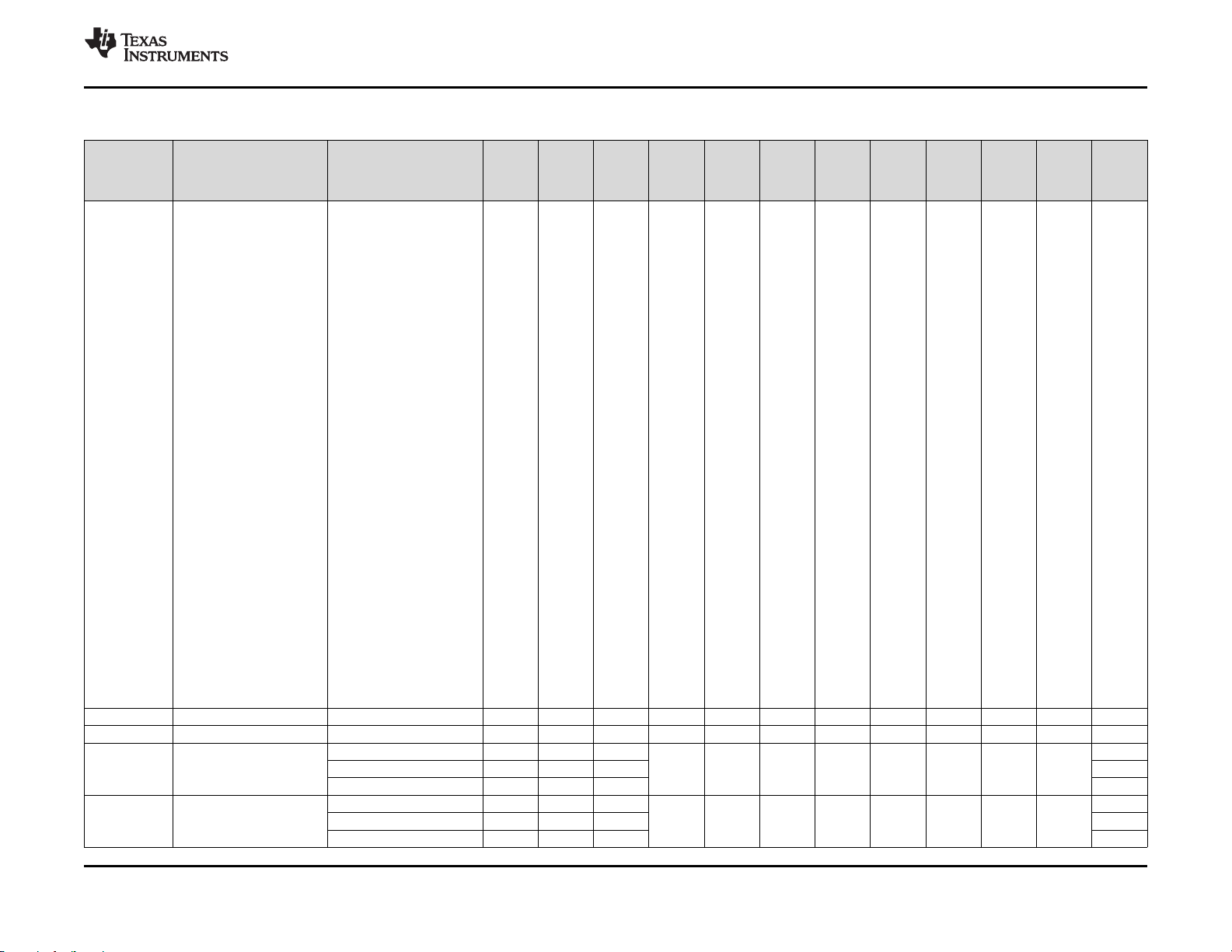
www.ti.com
DRA77P, DRA76P
SPRS993E –MARCH 2017–REVISED DECEMBER 2018
Table 4-1. Pin Attributes
BALL NUMBER [1] BALL NAME [2] SIGNAL NAME [3] 76x [4]
A1, A2, A28, AA10,
AA12, AA16, AA18,
AA20, AA22, AA8,
AB11, AB13, AB17,
AB9, AC12, AC15,
AD10, AD13, AD16,
AD19, AE11, AE14,
AE17, AF12, AF15,
AF18, AF9, AG1,
AG10, AG13,
AG16, AG28, AG4,
AG7, AH1, AH11,
AH14, AH17, AH2,
AH27, AH28, AH5,
AH8, B1, G12, G16,
G18, G20, G22, G8,
H13, H15, H17,
H19, H21, H23, H7,
H9, J10, J12, J14,
J18, J20, J22, J8,
K11, K13, K15,
K17, K19, K21,
K23, K7, K9, L10,
L12, L14, L16, L18,
L20, L22, L8, M11,
M13, M15, M17,
M19, M21, M23,
M7, M9, N10, N12,
N14, N16, N18,
N20, N22, N8, P11,
P13, P15, P17,
P19, P7, P9, R10,
R12, R16, R18,
R22, R8, T11, T13,
T15, T17, T19, T21,
T23, T7, T9, U10,
U12, U14, U16,
U18, U20, U22, U8,
V11, V13, V15,
V17, V19, V21,
V23, V7, V9, W10,
W12, W14, W16,
W18, W20, W22,
W8, Y11, Y13, Y15,
Y17, Y19, Y21,
Y23, Y7, Y9
AB15 vssa_osc0 vssa_osc0 GND
AC18 vssa_osc1 vssa_osc1 GND
AB19 Wakeup0 dcan1_rx 1 I OFF OFF 15 1.8/3.3 vddshv5 Yes IHHV1833 PU/PD 1
AC20 Wakeup1 dcan2_rx 1 I OFF OFF 15 1.8/3.3 vddshv5 Yes IHHV1833 PU/PD 1
vss vss GND
gpio1_0 14 I
Driver off 15 I
gpio1_1 14 I
Driver off 15 I
MUXMODE
[5]
TYPE [6]
(1)
(continued)
BALL
RESET
STATE [7]
BALL
RESET
REL.
STATE [8]
BALL
RESET
REL.
MUXMODE
[9]
I/O
VOLTAGE
VALUE [10]
POWER
[11]
HYS [12]
BUFFER
TYPE [13]
PULL
UP/DOWN
TYPE [14]
DSIS [15]
Copyright © 2017–2018, Texas Instruments Incorporated Terminal Configuration and Functions
Submit Documentation Feedback
Product Folder Links: DRA77P DRA76P
79

DRA77P, DRA76P
SPRS993E –MARCH 2017–REVISED DECEMBER 2018
www.ti.com
Table 4-1. Pin Attributes
BALL NUMBER [1] BALL NAME [2] SIGNAL NAME [3] 76x [4]
AB20 Wakeup2 sys_nirq2 1 I OFF OFF 15 1.8/3.3 vddshv5 Yes IHHV1833 PU/PD
gpio1_2 14 I
Driver off 15 I
AB21 Wakeup3 sys_nirq1 1 I OFF OFF 15 1.8/3.3 vddshv5 Yes IHHV1833 PU/PD
gpio1_3 14 I
Driver off 15 I
AB16 xi_osc0 xi_osc0 0 I 1.8 vdda_osc No LVCMOS
AC19 xi_osc1 xi_osc1 0 I 1.8 vdda_osc No LVCMOS
AB14 xo_osc0 xo_osc0 0 O 1.8 vdda_osc No LVCMOS
AB18 xo_osc1 xo_osc1 0 A 1.8 vdda_osc No LVCMOS
D18 xref_clk0 xref_clk0 0 I PD PD 15 1.8/3.3 vddshv3 Yes Dual
mcasp2_axr8 1 IO 0
mcasp1_axr4 2 IO 0
mcasp1_ahclkx 3 O
mcasp5_ahclkx 4 O
atl_clk0 5 O
hdq0 8 IO 1
clkout2 9 O
timer13 10 IO
gpio6_17 14 IO
Driver off 15 I
E17 xref_clk1 xref_clk1 0 I PD PD 15 1.8/3.3 vddshv3 Yes Dual
mcasp2_axr9 1 IO 0
mcasp1_axr5 2 IO 0
mcasp2_ahclkx 3 O
mcasp6_ahclkx 4 O
atl_clk1 5 O
timer14 10 IO
gpio6_18 14 IO
Driver off 15 I
MUXMODE
[5]
TYPE [6]
(1)
(continued)
BALL
RESET
STATE [7]
BALL
RESET
REL.
STATE [8]
BALL
RESET
REL.
MUXMODE
[9]
I/O
VOLTAGE
VALUE [10]
POWER
[11]
HYS [12]
BUFFER
TYPE [13]
Analog
Analog
Analog
Analog
Voltage
LVCMOS
Voltage
LVCMOS
PULL
UP/DOWN
TYPE [14]
PU/PD
PU/PD
DSIS [15]
80
Copyright © 2017–2018, Texas Instruments IncorporatedTerminal Configuration and Functions
Submit Documentation Feedback
Product Folder Links: DRA77P DRA76P

www.ti.com
DRA77P, DRA76P
SPRS993E –MARCH 2017–REVISED DECEMBER 2018
Table 4-1. Pin Attributes
BALL NUMBER [1] BALL NAME [2] SIGNAL NAME [3] 76x [4]
B25 xref_clk2 xref_clk2 0 I PD PD 15 1.8/3.3 vddshv3 Yes Dual
mcasp2_axr10 1 IO 0
mcasp1_axr6 2 IO 0
mcasp3_ahclkx 3 O
mcasp7_ahclkx 4 O
atl_clk2 5 O
vout2_clk 6 O
vin4a_clk0 8 I 0
timer15 10 IO
gpio6_19 14 IO
Driver off 15 I
A22 xref_clk3 xref_clk3 0 I PD PD 15 1.8/3.3 vddshv3 Yes Dual
mcasp2_axr11 1 IO 0
mcasp1_axr7 2 IO 0
mcasp4_ahclkx 3 O
mcasp8_ahclkx 4 O
atl_clk3 5 O
vout2_de 6 O
hdq0 7 IO 1
vin4a_de0 8 I 0
clkout3 9 O
timer16 10 IO
gpio6_20 14 IO
Driver off 15 I
MUXMODE
[5]
TYPE [6]
(1)
(continued)
BALL
RESET
STATE [7]
BALL
RESET
REL.
STATE [8]
BALL
RESET
REL.
MUXMODE
[9]
I/O
VOLTAGE
VALUE [10]
POWER
[11]
HYS [12]
BUFFER
TYPE [13]
Voltage
LVCMOS
Voltage
LVCMOS
PULL
UP/DOWN
TYPE [14]
PU/PD
PU/PD
DSIS [15]
(1) NA in this table stands for Not Applicable.
(2) For more information on recommended operating conditions, see Section 5.4, Recommended Operating Conditions.
(3) The pullup or pulldown block strength is equal to: minimum = 50 μA, typical = 100 μA, maximum = 250 μA.
(4) The output impedance settings of this IO cell are programmable; by default, the value is DS[1:0] = 10, this means 40 Ω. For more information on DS[1:0] register configuration, see the
Device TRM.
(5) IO drive strength for usb1_dp, usb1_dm, usb2_dp and usb2_dm: minimum 18.3 mA, maximum 89 mA (for a power supply vdda33v_usb1 and vdda33v_usb2 = 3.46 V).
(6) Minimum PU = 900 Ω, maximum PU = 3.090 kΩ and minimum PD = 14.25 kΩ, maximum PD = 24.8 kΩ.
For more information, see chapter 7 of the USB2.0 specification, in particular section Signaling / Device Speed Identification.
(7) This function will not be supported on some pin-compatibleroadmap devices. Pin compatibility can be maintained in the future by not using these GPIO signals.
(8) In PUx / PDy, x and y = 60 μA to 200 μA.
The output impedance settings (or drive strengths) of this IO are programmable (34 Ω, 40 Ω, 48 Ω, 60 Ω, 80 Ω) depending on the values of the I[2:0] registers.
(9) This signal is valid only for High-Security devices. For more details, see Section 5.8, VPP Specification for One-Time Programmable (OTP) eFUSEs. For General Purpose devices do not
connect any signal, test point, or board trace to this signal.
Copyright © 2017–2018, Texas Instruments Incorporated Terminal Configuration and Functions
Submit Documentation Feedback
Product Folder Links: DRA77P DRA76P
81

DRA77P, DRA76P
SPRS993E –MARCH 2017–REVISED DECEMBER 2018
4.3 Signal Descriptions
Many signals are available on multiple pins, according to the software configuration of the pin multiplexing
options.
1. SIGNAL NAME: The name of the signal passing through the pin.
The subsystem multiplexing signals are not described in Table 4-1 and Table 4-33.
2. DESCRIPTION: Description of the signal
3. TYPE: Signal direction and type:
– I = Input
– O = Output
– IO = Input or output
– D = Open Drain
– DS = Differential
– A = Analog
– PWR = Power
– GND = Ground
4. BALL: Associated ball(s) bottom
www.ti.com
NOTE
NOTE
For more information, see the Control Module / Control Module Register Manual section of
the Device TRM.
4.3.1 VIP
NOTE
For more information, see the Video Input Port (VIP) section of the Device TRM.
CAUTION
The I/O timings provided in Section 5.10, Timing Requirements and Switching
Characteristics are applicable for all combinations of signals for vin1. However,
the timings are only valid for vin2, vin3, and vin4 if signals within a single
IOSET are used. The IOSETs are defined in the Table 5-31, Table 5-32, and
Table 5-33.
Table 4-2. VIP Signal Descriptions
SIGNAL NAME DESCRIPTION TYPE BALL
Video Input 1
vin1a_clk0
vin1a_d0 Video Input 1 Port A Data input
vin1a_d1 Video Input 1 Port A Data input
vin1a_d2 Video Input 1 Port A Data input
vin1a_d3 Video Input 1 Port A Data input
vin1a_d4 Video Input 1 Port A Data input
vin1a_d5 Video Input 1 Port A Data input
vin1a_d6 Video Input 1 Port A Data input
Video Input 1 Port A Clock input. Input clock for 8-bit 16-bit or 24-bit Port A video
capture. Input data is sampled on the CLK0 edge.
(1)
(1)
(1)
(1)
(1)
(1)
(1)
I
I AE9
I AF10
I AE7
I AE8
I AE6
I AF7
I AF8
AD8
82
Terminal Configuration and Functions Copyright © 2017–2018, Texas Instruments Incorporated
Submit Documentation Feedback
Product Folder Links: DRA77P DRA76P

DRA77P, DRA76P
www.ti.com
SPRS993E –MARCH 2017–REVISED DECEMBER 2018
Table 4-2. VIP Signal Descriptions (continued)
SIGNAL NAME DESCRIPTION TYPE BALL
vin1a_d7 Video Input 1 Port A Data input
vin1a_d8 Video Input 1 Port A Data input
vin1a_d9 Video Input 1 Port A Data input
vin1a_d10 Video Input 1 Port A Data input
vin1a_d11 Video Input 1 Port A Data input
vin1a_d12 Video Input 1 Port A Data input
vin1a_d13 Video Input 1 Port A Data input
vin1a_d14 Video Input 1 Port A Data input
vin1a_d15 Video Input 1 Port A Data input
vin1a_d16 Video Input 1 Port A Data input
vin1a_d17 Video Input 1 Port A Data input
vin1a_d18 Video Input 1 Port A Data input
vin1a_d19 Video Input 1 Port A Data input
vin1a_d20 Video Input 1 Port A Data input
vin1a_d21 Video Input 1 Port A Data input
vin1a_d22 Video Input 1 Port A Data input
vin1a_d23 Video Input 1 Port A Data input
vin1a_de0 Video Input 1 Data Enable input
vin1a_fld0 Video Input 1 Port A Field ID input
vin1a_hsync0 Video Input 1 Port A Horizontal Sync input
vin1a_vsync0 Video Input 1 Port A Vertical Sync input
vin1b_clk1 Video Input 1 Port B Clock input
vin1b_d0 Video Input 1 Port B Data input
vin1b_d1 Video Input 1 Port B Data input
vin1b_d2 Video Input 1 Port B Data input
vin1b_d3 Video Input 1 Port B Data input
vin1b_d4 Video Input 1 Port B Data input
vin1b_d5 Video Input 1 Port B Data input
vin1b_d6 Video Input 1 Port B Data input
vin1b_d7 Video Input 1 Port B Data input
vin1b_de1 Video Input 1 Port B Data Enable input
vin1b_fld1 Video Input 1 Port B Field ID input
vin1b_hsync1 Video Input 1 Port B Horizontal Sync input
vin1b_vsync1 Video Input 1 Port B Vertical Sync input
Video Input 2
vin2a_clk0 Video Input 2 Port A Clock input I F1, V1
vin2a_d0 Video Input 2 Port A Data input I F2, U3
vin2a_d1 Video Input 2 Port A Data input I E3, V2
vin2a_d2 Video Input 2 Port A Data input I E1, Y1
vin2a_d3 Video Input 2 Port A Data input I E2, T6
vin2a_d4 Video Input 2 Port A Data input I D2, U5
vin2a_d5 Video Input 2 Port A Data input I F3, U4
vin2a_d6 Video Input 2 Port A Data input I D1, V4
vin2a_d7 Video Input 2 Port A Data input I E4, W2
vin2a_d8 Video Input 2 Port A Data input I G3, V3
vin2a_d9 Video Input 2 Port A Data input I C5, Y2
vin2a_d10 Video Input 2 Port A Data input I D3, T5
(1)
(1)
(1)
(1)
(1)
(1)
(1)
(1)
(1)
(1)
(1)
(1)
(1)
(1)
(1)
(1)
(1)
(1)
(1)
(1)
(1)
(1)
(1)
(1)
(1)
(1)
(1)
(1)
(1)
(1)
(1)
(1)
(1)
(1)
I AF6
I AF4
I AF2
I AF3
I AF5
I AE5
I AF1
I AD6
I AE3
I AE4
I AE1
I AD5
I AD3
I AD4
I AE2
I AD1
I AD2
I AC9
I AD9
I AC10
I AD7
I AC8
I AD2, AE3
I AD1, AD6
I AE2, AF1
I AD4, AE5
I AD3, AF5
I AD5, AF3
I AE1, AF2
I AE4, AF4
I AD7, M4
I AC10
I AC9, N3
I AD9
Submit Documentation Feedback
Product Folder Links: DRA77P DRA76P
Terminal Configuration and FunctionsCopyright © 2017–2018, Texas Instruments Incorporated
83

DRA77P, DRA76P
SPRS993E –MARCH 2017–REVISED DECEMBER 2018
Table 4-2. VIP Signal Descriptions (continued)
SIGNAL NAME DESCRIPTION TYPE BALL
vin2a_d11 Video Input 2 Port A Data input I F4, U2
vin2a_d12 Video Input 2 Port A Data input I E6
vin2a_d13 Video Input 2 Port A Data input I C1
vin2a_d14 Video Input 2 Port A Data input I C2
vin2a_d15 Video Input 2 Port A Data input I C3
vin2a_d16 Video Input 2 Port A Data input I B2
vin2a_d17 Video Input 2 Port A Data input I B5
vin2a_d18 Video Input 2 Port A Data input I D4
vin2a_d19 Video Input 2 Port A Data input I A3
vin2a_d20 Video Input 2 Port A Data input I B3
vin2a_d21 Video Input 2 Port A Data input I B4
vin2a_d22 Video Input 2 Port A Data input I C4
vin2a_d23 Video Input 2 Port A Data input I A4
vin2a_de0 Video Input 2 Port A Data Enable input I G2, T4
vin2a_fld0 Video Input 2 Port A Field ID input I D5, G2, W1
vin2a_hsync0 Video Input 2 Port A Horizontal Sync input I G1, T3
vin2a_vsync0 Video Input 2 Port A Vertical Sync input I E5, U6
vin2b_clk1 Video Input 2 Port B Clock input I AA5, D5
vin2b_d0 Video Input 2 Port B Data input I A4, AB5
vin2b_d1 Video Input 2 Port B Data input I AA6, C4
vin2b_d2 Video Input 2 Port B Data input I AC4, B4
vin2b_d3 Video Input 2 Port B Data input I AC6, B3
vin2b_d4 Video Input 2 Port B Data input I A3, W6
vin2b_d5 Video Input 2 Port B Data input I D4, Y6
vin2b_d6 Video Input 2 Port B Data input I AC7, B5
vin2b_d7 Video Input 2 Port B Data input I AC3, B2
vin2b_de1 Video Input 2 Port B Data Enable input I AB7, G2
vin2b_fld1 Video Input 2 Port B Field ID input I G2
vin2b_hsync1 Video Input 2 Port B Horizontal Sync input I AC5, G1
vin2b_vsync1 Video Input 2 Port B Vertical Sync input I AB4, E5
Video Input 3
vin3a_clk0 Video Input 3 Port A Clock input I AC8, B10, P1
vin3a_d0 Video Input 3 Port A Data input I AE4, B7, N5
vin3a_d1 Video Input 3 Port A Data input I AE1, B8, M2
vin3a_d2 Video Input 3 Port A Data input I A6, AD5, L5
vin3a_d3 Video Input 3 Port A Data input I A7, AD3, M1
vin3a_d4 Video Input 3 Port A Data input I AD4, C9, K6
vin3a_d5 Video Input 3 Port A Data input I A8, AE2, L4
vin3a_d6 Video Input 3 Port A Data input I AD1, B9, L3
vin3a_d7 Video Input 3 Port A Data input I A9, AD2, L2
vin3a_d8 Video Input 3 Port A Data input I B2, E8, L1
vin3a_d9 Video Input 3 Port A Data input I B5, D8, K1
vin3a_d10 Video Input 3 Port A Data input I D4, D6, J1
vin3a_d11 Video Input 3 Port A Data input I A3, D7, J2
vin3a_d12 Video Input 3 Port A Data input I A5, B3, H1
vin3a_d13 Video Input 3 Port A Data input I B4, B6, K2
vin3a_d14 Video Input 3 Port A Data input I C4, C8, H2
www.ti.com
84
Terminal Configuration and Functions Copyright © 2017–2018, Texas Instruments Incorporated
Submit Documentation Feedback
Product Folder Links: DRA77P DRA76P

DRA77P, DRA76P
www.ti.com
SPRS993E –MARCH 2017–REVISED DECEMBER 2018
Table 4-2. VIP Signal Descriptions (continued)
SIGNAL NAME DESCRIPTION TYPE BALL
vin3a_d15 Video Input 3 Port A Data input I A4, C7, K3
vin3a_d16 Video Input 3 Port A Data input I F9, P6
vin3a_d17 Video Input 3 Port A Data input I E10, J6
vin3a_d18 Video Input 3 Port A Data input I D9, R4
vin3a_d19 Video Input 3 Port A Data input I C6, R5
vin3a_d20 Video Input 3 Port A Data input I E9, M6
vin3a_d21 Video Input 3 Port A Data input I F8, K4
vin3a_d22 Video Input 3 Port A Data input I F7, P5
vin3a_d23 Video Input 3 Port A Data input I E7, N6
vin3a_de0 Video Input 3 Port A Data Enable input I B3, C10, J5
vin3a_fld0 Video Input 3 Port A Field ID input I B4, D11, K5
vin3a_hsync0 Video Input 3 Port A Horizontal Sync input I A10, C4, N4
vin3a_vsync0 Video Input 3 Port A Vertical Sync input I A4, D10, R3
vin3b_clk1 Video Input 3 Port B Clock input I L6, M4
vin3b_d0 Video Input 3 Port B Data input I H6
vin3b_d1 Video Input 3 Port B Data input I G6
vin3b_d2 Video Input 3 Port B Data input I J4
vin3b_d3 Video Input 3 Port B Data input I F5
vin3b_d4 Video Input 3 Port B Data input I G5
vin3b_d5 Video Input 3 Port B Data input I J3
vin3b_d6 Video Input 3 Port B Data input I H4
vin3b_d7 Video Input 3 Port B Data input I H3
vin3b_de1 Video Input 3 Port B Data Enable input I N3
vin3b_fld1 Video Input 3 Port A Field ID input I M4
vin3b_hsync1 Video Input 3 Port A Horizontal Sync input I H5
vin3b_vsync1 Video Input 3 Port A Vertical Sync input I G4
Video Input 4
vin4a_clk0 Video Input 4 Port A Clock input I B10, B25, P4
vin4a_d0 Video Input 4 Port A Data input I A13, B7, P6
vin4a_d1 Video Input 4 Port A Data input I B8, F14, J6
vin4a_d2 Video Input 4 Port A Data input I A6, E13, R4
vin4a_d3 Video Input 4 Port A Data input I A7, E11, R5
vin4a_d4 Video Input 4 Port A Data input I C9, E12, M6
vin4a_d5 Video Input 4 Port A Data input I A8, D13, K4
vin4a_d6 Video Input 4 Port A Data input I B9, C11, P5
vin4a_d7 Video Input 4 Port A Data input I A9, D12, N6
vin4a_d8 Video Input 4 Port A Data input I E15, E8, T2
vin4a_d9 Video Input 4 Port A Data input I A19, D8, U1
vin4a_d10 Video Input 4 Port A Data input I B14, D6, P3
vin4a_d11 Video Input 4 Port A Data input I A14, D7, R1
vin4a_d12 Video Input 4 Port A Data input I A5, D15, H6
vin4a_d13 Video Input 4 Port A Data input I B15, B6, G6
vin4a_d14 Video Input 4 Port A Data input I B16, C8, J4
vin4a_d15 Video Input 4 Port A Data input I A16, C7, F5
vin4a_d16 Video Input 4 Port A Data input I C17, F9
vin4a_d17 Video Input 4 Port A Data input I A20, E10
vin4a_d18 Video Input 4 Port A Data input I D16, D9
Submit Documentation Feedback
Product Folder Links: DRA77P DRA76P
Terminal Configuration and FunctionsCopyright © 2017–2018, Texas Instruments Incorporated
85

DRA77P, DRA76P
SPRS993E –MARCH 2017–REVISED DECEMBER 2018
www.ti.com
Table 4-2. VIP Signal Descriptions (continued)
SIGNAL NAME DESCRIPTION TYPE BALL
vin4a_d19 Video Input 4 Port A Data input I C6, D17
vin4a_d20 Video Input 4 Port A Data input I AA3, E9
vin4a_d21 Video Input 4 Port A Data input I AB6, F8
vin4a_d22 Video Input 4 Port A Data input I AB3, F7
vin4a_d23 Video Input 4 Port A Data input I AA4, E7
vin4a_de0 Video Input 4 Port A Data Enable input I A22, C10, G4, L6
vin4a_fld0 Video Input 4 Port A Field ID input I D11, F18, G5, K5
vin4a_hsync0 Video Input 4 Port A Horizontal Sync input I A10, E21, L6, R2
vin4a_vsync0 Video Input 4 Port A Vertical Sync input I D10, F17, N1, R6
vin4b_clk1 Video Input 4 Port B Clock input I J5, V1
vin4b_d0 Video Input 4 Port B Data input I P6, U3
vin4b_d1 Video Input 4 Port B Data input I J6, V2
vin4b_d2 Video Input 4 Port B Data input I R4, Y1
vin4b_d3 Video Input 4 Port B Data input I R5, T6
vin4b_d4 Video Input 4 Port B Data input I M6, U5
vin4b_d5 Video Input 4 Port B Data input I K4, U4
vin4b_d6 Video Input 4 Port B Data input I P5, V4
vin4b_d7 Video Input 4 Port B Data input I N6, W2
vin4b_de1 Video Input 4 Port B Data Enable input I K5, T4
vin4b_fld1 Video Input 4 Port B Field ID input I P4, W1
vin4b_hsync1 Video Input 4 Port B Horizontal Sync input I N4, T3
vin4b_vsync1 Video Input 4 Port B Vertical Sync input I R3, U6
(1) The VIP1 interface (Video Input 1a and Video Input 1b in Table 4-2) signal sets are NOT supported in the DRA76xP device. For more
details on the device differentiation, refer to the Table 3-1, Device Comparison.
4.3.2 DSS
CAUTION
The I/O timings provided in Section 5.10, Timing Requirements and Switching
Characteristics are valid only if signals within a single IOSET are used. The
IOSETs are defined in Table 5-45 and Table 5-46.
Table 4-3. DSS Signal Descriptions
SIGNAL NAME DESCRIPTION TYPE BALL
DPI Video Output 1
vout1_clk Video Output 1 Clock output O D11
vout1_de Video Output 1 Data Enable output O C10
vout1_fld Video Output 1 Field ID output. This signal is not used for embedded sync modes. O B10
vout1_hsync
vout1_vsync Video Output 1 Vertical Sync output. This signal is not used for embedded sync modes. O D10
vout1_d0 Video Output 1 Data output O F9
vout1_d1 Video Output 1 Data output O E10
vout1_d2 Video Output 1 Data output O D9
vout1_d3 Video Output 1 Data output O C6
vout1_d4 Video Output 1 Data output O E9
vout1_d5 Video Output 1 Data output O F8
Video Output 1 Horizontal Sync output. This signal is not used for embedded sync
modes.
O
A10
86
Terminal Configuration and Functions Copyright © 2017–2018, Texas Instruments Incorporated
Submit Documentation Feedback
Product Folder Links: DRA77P DRA76P

DRA77P, DRA76P
www.ti.com
SPRS993E –MARCH 2017–REVISED DECEMBER 2018
Table 4-3. DSS Signal Descriptions (continued)
SIGNAL NAME DESCRIPTION TYPE BALL
vout1_d6 Video Output 1 Data output O F7
vout1_d7 Video Output 1 Data output O E7
vout1_d8 Video Output 1 Data output O E8
vout1_d9 Video Output 1 Data output O D8
vout1_d10 Video Output 1 Data output O D6
vout1_d11 Video Output 1 Data output O D7
vout1_d12 Video Output 1 Data output O A5
vout1_d13 Video Output 1 Data output O B6
vout1_d14 Video Output 1 Data output O C8
vout1_d15 Video Output 1 Data output O C7
vout1_d16 Video Output 1 Data output O B7
vout1_d17 Video Output 1 Data output O B8
vout1_d18 Video Output 1 Data output O A6
vout1_d19 Video Output 1 Data output O A7
vout1_d20 Video Output 1 Data output O C9
vout1_d21 Video Output 1 Data output O A8
vout1_d22 Video Output 1 Data output O B9
vout1_d23 Video Output 1 Data output O A9
DPI Video Output 2
vout2_clk Video Output 2 Clock output O B25, D5
vout2_de Video Output 2 Data Enable output O A22, G2
vout2_fld Video Output 2 Field ID output. This signal is not used for embedded sync modes. O F1, F18
vout2_hsync
vout2_vsync Video Output 2 Vertical Sync output. This signal is not used for embedded sync modes. O E5, F17
vout2_d0 Video Output 2 Data output O A13, A4
vout2_d1 Video Output 2 Data output O C4, F14
vout2_d2 Video Output 2 Data output O B4, E13
vout2_d3 Video Output 2 Data output O B3, E11
vout2_d4 Video Output 2 Data output O A3, E12
vout2_d5 Video Output 2 Data output O D13, D4
vout2_d6 Video Output 2 Data output O B5, C11
vout2_d7 Video Output 2 Data output O B2, D12
vout2_d8 Video Output 2 Data output O C3, E15
vout2_d9 Video Output 2 Data output O A19, C2
vout2_d10 Video Output 2 Data output O B14, C1
vout2_d11 Video Output 2 Data output O A14, E6
vout2_d12 Video Output 2 Data output O D15, F4
vout2_d13 Video Output 2 Data output O B15, D3
vout2_d14 Video Output 2 Data output O B16, C5
vout2_d15 Video Output 2 Data output O A16, G3
vout2_d16 Video Output 2 Data output O C17, E4
vout2_d17 Video Output 2 Data output O A20, D1
vout2_d18 Video Output 2 Data output O D16, F3
vout2_d19 Video Output 2 Data output O D17, D2
vout2_d20 Video Output 2 Data output O AA3, E2
vout2_d21 Video Output 2 Data output O AB6, E1
vout2_d22 Video Output 2 Data output O AB3, E3
Video Output 2 Horizontal Sync output. This signal is not used for embedded sync
modes.
O
E21, G1
Submit Documentation Feedback
Product Folder Links: DRA77P DRA76P
Terminal Configuration and FunctionsCopyright © 2017–2018, Texas Instruments Incorporated
87

DRA77P, DRA76P
SPRS993E –MARCH 2017–REVISED DECEMBER 2018
Table 4-3. DSS Signal Descriptions (continued)
SIGNAL NAME DESCRIPTION TYPE BALL
vout2_d23 Video Output 2 Data output O AA4, F2
DPI Video Output 3
vout3_clk Video Output 3 Clock output O AD9, P1
vout3_de Video Output 3 Data Enable output O AC9, J5
vout3_fld Video Output 3 Field ID output. This signal is not used for embedded sync modes. O AD8, K5
vout3_hsync
vout3_vsync Video Output 3 Vertical Sync output. This signal is not used for embedded sync modes. O AD7, R3
vout3_d0 Video Output 3 Data output O AD2, AF6, N5
vout3_d1 Video Output 3 Data output O AD1, AF8, M2
vout3_d2 Video Output 3 Data output O AE2, AF7, L5
vout3_d3 Video Output 3 Data output O AD4, AE6, M1
vout3_d4 Video Output 3 Data output O AD3, AE8, K6
vout3_d5 Video Output 3 Data output O AD5, AE7, L4
vout3_d6 Video Output 3 Data output O AE1, AF10, L3
vout3_d7 Video Output 3 Data output O AE4, AE9, L2
vout3_d8 Video Output 3 Data output O AE3, L1
vout3_d9 Video Output 3 Data output O AD6, K1
vout3_d10 Video Output 3 Data output O AF1, J1
vout3_d11 Video Output 3 Data output O AE5, J2
vout3_d12 Video Output 3 Data output O AF5, H1
vout3_d13 Video Output 3 Data output O AF3, K2
vout3_d14 Video Output 3 Data output O AF2, H2
vout3_d15 Video Output 3 Data output O AF4, K3
vout3_d16 Video Output 3 Data output O AD8, AF6, P6
vout3_d17 Video Output 3 Data output O AC9, AF8, J6
vout3_d18 Video Output 3 Data output O AF7, R4
vout3_d19 Video Output 3 Data output O AE6, R5
vout3_d20 Video Output 3 Data output O AE8, M6
vout3_d21 Video Output 3 Data output O AE7, K4
vout3_d22 Video Output 3 Data output O AF10, P5
vout3_d23 Video Output 3 Data output O AE9, N6
Video Output 3 Horizontal Sync output. This signal is not used for embedded sync
modes.
O
AC10, N4
www.ti.com
4.3.3 HDMI
NOTE
For more information, see the Display Subsystem / Display Subsystem Overview of the
Device TRM.
Table 4-4. HDMI Signal Descriptions
SIGNAL NAME DESCRIPTION TYPE BALL
hdmi1_clockx HDMI clock differential positive or negative O AG14
hdmi1_clocky HDMI clock differential positive or negative O AH15
hdmi1_data0x HDMI data 0 differential positive or negative O AG15
hdmi1_data0y HDMI data 0 differential positive or negative O AH16
hdmi1_data1x HDMI data 1 differential positive or negative O AG17
hdmi1_data1y HDMI data 1 differential positive or negative O AH18
88
Terminal Configuration and Functions Copyright © 2017–2018, Texas Instruments Incorporated
Submit Documentation Feedback
Product Folder Links: DRA77P DRA76P

DRA77P, DRA76P
www.ti.com
SPRS993E –MARCH 2017–REVISED DECEMBER 2018
Table 4-4. HDMI Signal Descriptions (continued)
SIGNAL NAME DESCRIPTION TYPE BALL
hdmi1_data2x HDMI data 2 differential positive or negative O AG18
hdmi1_data2y HDMI data 2 differential positive or negative O AH19
hdmi1_cec HDMI consumer electronic control IO B19, D19
hdmi1_ddc_scl HDMI display data channel clock IO C24
hdmi1_ddc_sda HDMI display data channel data IO F15
hdmi1_hpd HDMI display hot plug detect I B20, E19
4.3.4 Camera Serial Interface 2 CAL bridge (CSI2)
NOTE
For more information, see the CAL Subsystem / CAL Subsystem Overview of the Device
TRM.
Table 4-5. CSI 2 Signal Descriptions
SIGNAL NAME DESCRIPTION TYPE BALL
csi2_0_dx0 Serial data/clock input - line 0 (position 1) I AD17
csi2_0_dx1 Serial data/clock input - line 1 (position 2) I AF16
csi2_0_dx2 Serial data/clock input - line 2 (position 3) I AF19
csi2_0_dx3 Serial data/clock input - line 3 (position 4) I AE15
csi2_0_dx4 Serial data input only - line 4 (position 5)
csi2_0_dy0 Serial data/clock input - line 0 (position 1) I AD18
csi2_0_dy1 Serial data/clock input - line 1 (position 2) I AF17
csi2_0_dy2 Serial data/clock input - line 2 (position 3) I AF20
csi2_0_dy3 Serial data/clock input - line 3 (position 4) I AE16
csi2_0_dy4 Serial data input only - line 4 (position 5)
csi2_1_dx0 Serial data/clock input - line 0 (position 1) I AC13
csi2_1_dx1 Serial data/clock input - line 1 (position 2) I AD15
csi2_1_dx2 Serial data/clock input - line 2 (position 3) I AC16
csi2_1_dy0 Serial data/clock input - line 0 (position 1) I AC14
csi2_1_dy1 Serial data/clock input - line 1 (position 2) I AD14
csi2_1_dy2 Serial data/clock input - line 2 (position 3) I AC17
(1) Line 4 (position 5) supports only data. For more information, see CAL Subsystem of the Device TRM.
(1)
(1)
I AE19
I AE18
4.3.5 EMIF
NOTE
For more information, see the Memory Subsystem / EMIF Controller section of the Device
TRM.
NOTE
The index numbers 1 and 2 which are part of the EMIF1 and EMIF2 signal prefixes (ddr1_*
and ddr2_*) listed in Table 4-6, EMIF Signal Descriptions, not to be confused with DDR1 and
DDR2 types of SDRAM memories.
Terminal Configuration and FunctionsCopyright © 2017–2018, Texas Instruments Incorporated
Submit Documentation Feedback
Product Folder Links: DRA77P DRA76P
89

DRA77P, DRA76P
SPRS993E –MARCH 2017–REVISED DECEMBER 2018
Table 4-6. EMIF Signal Descriptions
SIGNAL NAME DESCRIPTION TYPE BALL
EMIF Channel 1
ddr1_casn EMIF1 Column Address Strobe O AG19
ddr1_ck EMIF1 Clock O AG24
ddr1_cke EMIF1 Clock Enable O AH23
ddr1_dqm_ecc EMIF1 ECC Data Mask O T27
ddr1_dqsn_ecc EMIF1 ECC Complementary Data Strobe IO U28
ddr1_dqs_ecc
ddr1_nck EMIF1 Negative Clock O AH24
ddr1_rasn EMIF1 Row Address Strobe O AH20
ddr1_rst EMIF1 Reset output (DDR3-SDRAM only) O AF23
ddr1_wen EMIF1 Write Enable O AG22
ddr1_a0 EMIF1 Address Bus O AE22
ddr1_a1 EMIF1 Address Bus O AD20
ddr1_a2 EMIF1 Address Bus O AE21
ddr1_a3 EMIF1 Address Bus O AD22
ddr1_a4 EMIF1 Address Bus O AE23
ddr1_a5 EMIF1 Address Bus O AH22
ddr1_a6 EMIF1 Address Bus O AD24
ddr1_a7 EMIF1 Address Bus O AC22
ddr1_a8 EMIF1 Address Bus O AG23
ddr1_a9 EMIF1 Address Bus O AF24
ddr1_a10 EMIF1 Address Bus O AD21
ddr1_a11 EMIF1 Address Bus O AE24
ddr1_a12 EMIF1 Address Bus O AG21
ddr1_a13 EMIF1 Address Bus O AF21
ddr1_a14 EMIF1 Address Bus O AC23
ddr1_a15 EMIF1 Address Bus O AG20
ddr1_ba0 EMIF1 Bank Address O AE20
ddr1_ba1 EMIF1 Bank Address O AC21
ddr1_ba2 EMIF1 Bank Address O AH21
ddr1_csn0 EMIF1 Chip Select 0 O AD23
ddr1_d0 EMIF1 Data Bus IO AE26
ddr1_d1 EMIF1 Data Bus IO AE27
ddr1_d2 EMIF1 Data Bus IO AF28
ddr1_d3 EMIF1 Data Bus IO AH26
ddr1_d4 EMIF1 Data Bus IO AF25
ddr1_d5 EMIF1 Data Bus IO AG27
ddr1_d6 EMIF1 Data Bus IO AF27
ddr1_d7 EMIF1 Data Bus IO AF26
ddr1_d8 EMIF1 Data Bus IO AB24
ddr1_d9 EMIF1 Data Bus IO AD27
ddr1_d10 EMIF1 Data Bus IO AE28
ddr1_d11 EMIF1 Data Bus IO AD28
ddr1_d12 EMIF1 Data Bus IO AD26
ddr1_d13 EMIF1 Data Bus IO AE25
ddr1_d14 EMIF1 Data Bus IO AD25
EMIF1 ECC Data Strobe input/output. This signal is output to the EMIF1 memory when
writing and input when reading.
IO U27
www.ti.com
90
Terminal Configuration and Functions Copyright © 2017–2018, Texas Instruments Incorporated
Submit Documentation Feedback
Product Folder Links: DRA77P DRA76P

DRA77P, DRA76P
www.ti.com
SPRS993E –MARCH 2017–REVISED DECEMBER 2018
Table 4-6. EMIF Signal Descriptions (continued)
SIGNAL NAME DESCRIPTION TYPE BALL
ddr1_d15 EMIF1 Data Bus IO AC26
ddr1_d16 EMIF1 Data Bus IO AA25
ddr1_d17 EMIF1 Data Bus IO AB25
ddr1_d18 EMIF1 Data Bus IO AA26
ddr1_d19 EMIF1 Data Bus IO AA28
ddr1_d20 EMIF1 Data Bus IO AA27
ddr1_d21 EMIF1 Data Bus IO AA24
ddr1_d22 EMIF1 Data Bus IO AC25
ddr1_d23 EMIF1 Data Bus IO Y26
ddr1_d24 EMIF1 Data Bus IO W26
ddr1_d25 EMIF1 Data Bus IO AB23
ddr1_d26 EMIF1 Data Bus IO V24
ddr1_d27 EMIF1 Data Bus IO Y24
ddr1_d28 EMIF1 Data Bus IO W25
ddr1_d29 EMIF1 Data Bus IO Y25
ddr1_d30 EMIF1 Data Bus IO W24
ddr1_d31 EMIF1 Data Bus IO Y28
ddr1_dqm0 EMIF1 Data Mask O AG26
ddr1_dqm1 EMIF1 Data Mask O AC24
ddr1_dqm2 EMIF1 Data Mask O AB26
ddr1_dqm3 EMIF1 Data Mask O Y27
ddr1_dqs0
ddr1_dqs1
ddr1_dqs2
ddr1_dqs3
ddr1_dqsn0 Data strobe 0 invert IO AG25
ddr1_dqsn1 Data strobe 1 invert IO AC28
ddr1_dqsn2 Data strobe 2 invert IO AB28
ddr1_dqsn3 Data strobe 3 invert IO W27
ddr1_ecc_d0 EMIF1 ECC Data Bus
ddr1_ecc_d1 EMIF1 ECC Data Bus
ddr1_ecc_d2 EMIF1 ECC Data Bus
ddr1_ecc_d3 EMIF1 ECC Data Bus
ddr1_ecc_d4 EMIF1 ECC Data Bus
ddr1_ecc_d5 EMIF1 ECC Data Bus
ddr1_ecc_d6 EMIF1 ECC Data Bus
ddr1_ecc_d7 EMIF1 ECC Data Bus
ddr1_odt0 EMIF1 On-Die Termination for Chip Select 0 O AF22
EMIF Channel 2
ddr2_casn EMIF2 Column Address Strobe O T25
ddr2_ck EMIF2 Clock O R28
ddr2_cke EMIF2 Clock Enable O R25
ddr2_nck EMIF2 Negative Clock O R27
ddr2_rasn EMIF2 Row Address Strobe O R26
Data strobe 0 input/output for byte 0 of the 32-bit data bus. This signal is output to the
EMIF1 memory when writing and input when reading.
Data strobe 1 input/output for byte 1 of the 32-bit data bus. This signal is output to the
EMIF1 memory when writing and input when reading.
Data strobe 2 input/output for byte 2 of the 32-bit data bus. This signal is output to the
EMIF1 memory when writing and input when reading.
Data strobe 3 input/output for byte 3 of the 32-bit data bus. This signal is output to the
EMIF1 memory when writing and input when reading.
(1)
(1)
(1)
(1)
(1)
(1)
(1)
(1)
IO AH25
IO AC27
IO AB27
IO W28
IO U25
IO U26
IO V25
IO V26
IO V27
IO T28
IO T26
IO V28
Submit Documentation Feedback
Product Folder Links: DRA77P DRA76P
Terminal Configuration and FunctionsCopyright © 2017–2018, Texas Instruments Incorporated
91

DRA77P, DRA76P
SPRS993E –MARCH 2017–REVISED DECEMBER 2018
Table 4-6. EMIF Signal Descriptions (continued)
SIGNAL NAME DESCRIPTION TYPE BALL
ddr2_rst EMIF2 Reset output (DDR3-SDRAM only) O N25
ddr2_wen EMIF2 Write Enable O T24
ddr2_a0 EMIF2 Address Bus O P25
ddr2_a1 EMIF2 Address Bus O P26
ddr2_a2 EMIF2 Address Bus O P28
ddr2_a3 EMIF2 Address Bus O P27
ddr2_a4 EMIF2 Address Bus O P24
ddr2_a5 EMIF2 Address Bus O P23
ddr2_a6 EMIF2 Address Bus O N26
ddr2_a7 EMIF2 Address Bus O M25
ddr2_a8 EMIF2 Address Bus O N28
ddr2_a9 EMIF2 Address Bus O M27
ddr2_a10 EMIF2 Address Bus O L25
ddr2_a11 EMIF2 Address Bus O N27
ddr2_a12 EMIF2 Address Bus O M28
ddr2_a13 EMIF2 Address Bus O R24
ddr2_a14 EMIF2 Address Bus O N24
ddr2_a15 EMIF2 Address Bus O R23
ddr2_ba0 EMIF2 Bank Address O L24
ddr2_ba1 EMIF2 Bank Address O U24
ddr2_ba2 EMIF2 Bank Address O M24
ddr2_csn0 EMIF2 Chip Select 0 O M26
ddr2_d0 EMIF2 Data Bus IO C28
ddr2_d1 EMIF2 Data Bus IO A26
ddr2_d2 EMIF2 Data Bus IO E24
ddr2_d3 EMIF2 Data Bus IO D25
ddr2_d4 EMIF2 Data Bus IO D26
ddr2_d5 EMIF2 Data Bus IO B27
ddr2_d6 EMIF2 Data Bus IO B26
ddr2_d7 EMIF2 Data Bus IO C26
ddr2_d8 EMIF2 Data Bus IO F26
ddr2_d9 EMIF2 Data Bus IO E25
ddr2_d10 EMIF2 Data Bus IO E26
ddr2_d11 EMIF2 Data Bus IO G27
ddr2_d12 EMIF2 Data Bus IO E28
ddr2_d13 EMIF2 Data Bus IO G26
ddr2_d14 EMIF2 Data Bus IO G28
ddr2_d15 EMIF2 Data Bus IO F25
ddr2_d16 EMIF2 Data Bus IO G25
ddr2_d17 EMIF2 Data Bus IO G24
ddr2_d18 EMIF2 Data Bus IO F23
ddr2_d19 EMIF2 Data Bus IO F24
ddr2_d20 EMIF2 Data Bus IO H28
ddr2_d21 EMIF2 Data Bus IO H25
ddr2_d22 EMIF2 Data Bus IO H27
ddr2_d23 EMIF2 Data Bus IO H26
ddr2_d24 EMIF2 Data Bus IO K27
www.ti.com
92
Terminal Configuration and Functions Copyright © 2017–2018, Texas Instruments Incorporated
Submit Documentation Feedback
Product Folder Links: DRA77P DRA76P

DRA77P, DRA76P
www.ti.com
SPRS993E –MARCH 2017–REVISED DECEMBER 2018
Table 4-6. EMIF Signal Descriptions (continued)
SIGNAL NAME DESCRIPTION TYPE BALL
ddr2_d25 EMIF2 Data Bus IO K26
ddr2_d26 EMIF2 Data Bus IO J25
ddr2_d27 EMIF2 Data Bus IO K28
ddr2_d28 EMIF2 Data Bus IO H24
ddr2_d29 EMIF2 Data Bus IO J24
ddr2_d30 EMIF2 Data Bus IO K24
ddr2_d31 EMIF2 Data Bus IO L26
ddr2_dqm0 EMIF2 Data Mask O C27
ddr2_dqm1 EMIF2 Data Mask O E27
ddr2_dqm2 EMIF2 Data Mask O G23
ddr2_dqm3 EMIF2 Data Mask O J26
ddr2_dqs0
ddr2_dqs1
ddr2_dqs2
ddr2_dqs3
ddr2_dqsn0 Data strobe 0 invert IO D27
ddr2_dqsn1 Data strobe 1 invert IO F28
ddr2_dqsn2 Data strobe 2 invert IO J28
ddr2_dqsn3 Data strobe 3 invert IO L27
ddr2_odt0 EMIF2 On-Die Termination for Chip Select 0 O K25
(1) The ECC module (EMIF1 ECC Data Bus in Table 4-2) signal sets are NOT supported in the DRA76xP devices. For more details on
the device differentiation, refer to the Table 3-1, Device Comparison.
Data strobe 0 input/output for byte 0 of the 32-bit data bus. This signal is output to the
EMIF2 memory when writing and input when reading.
Data strobe 1 input/output for byte 1 of the 32-bit data bus. This signal is output to the
EMIF2 memory when writing and input when reading.
Data strobe 2 input/output for byte 2 of the 32-bit data bus. This signal is output to the
EMIF2 memory when writing and input when reading.
Data strobe 3 input/output for byte 3 of the 32-bit data bus. This signal is output to the
EMIF2 memory when writing and input when reading.
IO D28
IO F27
IO J27
IO L28
4.3.6 GPMC
NOTE
For more information, see the Memory Subsystem / General-Purpose Memory Controller
section of the Device TRM.
Table 4-7. GPMC Signal Descriptions
SIGNAL NAME DESCRIPTION TYPE BALL
gpmc_a0
gpmc_a1
gpmc_a2
gpmc_a3
gpmc_a4
gpmc_a5
gpmc_a6
gpmc_a7
GPMC Address 0. Only used to effectively address 8-bit data
nonmultiplexed memories
GPMC address 1 in A/D nonmultiplexed mode and Adress 17 in A/D
multiplexed mode
GPMC address 2 in A/D nonmultiplexed mode and Adress 18 in A/D
multiplexed mode
GPMC address 3 in A/D nonmultiplexed mode and Address 19 in A/D
multiplexed mode
GPMC address 4 in A/D nonmultiplexed mode and Address 20 in A/D
multiplexed mode
GPMC address 5 in A/D nonmultiplexed mode and Address 21 in A/D
multiplexed mode
GPMC address 6 in A/D nonmultiplexed mode and Address 22 in A/D
multiplexed mode
GPMC address 7 in A/D nonmultiplexed mode and Address 23 in A/D
multiplexed mode
O P4, P6
O J6, P1
O N1, R4
O M4, R5
O M6
O K4
O P5
O N6
Submit Documentation Feedback
Product Folder Links: DRA77P DRA76P
Terminal Configuration and FunctionsCopyright © 2017–2018, Texas Instruments Incorporated
93

DRA77P, DRA76P
SPRS993E –MARCH 2017–REVISED DECEMBER 2018
Table 4-7. GPMC Signal Descriptions (continued)
SIGNAL NAME DESCRIPTION TYPE BALL
gpmc_a8
gpmc_a9
gpmc_a10
gpmc_a11
gpmc_a12
gpmc_a13
gpmc_a14
gpmc_a15
gpmc_a16
gpmc_a17
gpmc_a18
gpmc_a19
gpmc_a20
gpmc_a21
gpmc_a22
gpmc_a23
gpmc_a24
gpmc_a25
gpmc_a26
gpmc_a27
gpmc_ad0
gpmc_ad1
gpmc_ad2
gpmc_ad3
gpmc_ad4
gpmc_ad5
gpmc_ad6
gpmc_ad7
GPMC address 8 in A/D nonmultiplexed mode and Address 24 in A/D
multiplexed mode
GPMC address 9 in A/D nonmultiplexed mode and Address 25 in A/D
multiplexed mode
GPMC address 10 in A/D nonmultiplexed mode and Address 26 in A/D
multiplexed mode
GPMC address 11 in A/D nonmultiplexed mode and unused in A/D
multiplexed mode
GPMC address 12 in A/D nonmultiplexed mode and unused in A/D
multiplexed mode
GPMC address 13 in A/D nonmultiplexed mode and unused in A/D
multiplexed mode
GPMC address 14 in A/D nonmultiplexed mode and unused in A/D
multiplexed mode
GPMC address 15 in A/D nonmultiplexed mode and unused in A/D
multiplexed mode
GPMC address 16 in A/D nonmultiplexed mode and unused in A/D
multiplexed mode
GPMC address 17 in A/D nonmultiplexed mode and unused in A/D
multiplexed mode
GPMC address 18 in A/D nonmultiplexed mode and unused in A/D
multiplexed mode
GPMC address 19 in A/D nonmultiplexed mode and unused in A/D
multiplexed mode
GPMC address 20 in A/D nonmultiplexed mode and unused in A/D
multiplexed mode
GPMC address 21 in A/D nonmultiplexed mode and unused in A/D
multiplexed mode
GPMC address 22 in A/D nonmultiplexed mode and unused in A/D
multiplexed mode
GPMC address 23 in A/D nonmultiplexed mode and unused in A/D
multiplexed mode
GPMC address 24 in A/D nonmultiplexed mode and unused in A/D
multiplexed mode
GPMC address 25 in A/D nonmultiplexed mode and unused in A/D
multiplexed mode
GPMC address 26 in A/D nonmultiplexed mode and unused in A/D
multiplexed mode
GPMC address 27 in A/D nonmultiplexed mode and Address 27 in A/D
multiplexed mode
GPMC Data 0 in A/D nonmultiplexed mode and additionally Address 1
in A/D multiplexed mode
GPMC Data 1 in A/D nonmultiplexed mode and additionally Address 2
in A/D multiplexed mode
GPMC Data 2 in A/D nonmultiplexed mode and additionally Address 3
in A/D multiplexed mode
GPMC Data 3 in A/D nonmultiplexed mode and additionally Address 4
in A/D multiplexed mode
GPMC Data 4 in A/D nonmultiplexed mode and additionally Address 5
in A/D multiplexed mode
GPMC Data 5 in A/D nonmultiplexed mode and additionally Address 6
in A/D multiplexed mode
GPMC Data 6 in A/D nonmultiplexed mode and additionally Address 7
in A/D multiplexed mode
GPMC Data 7 in A/D nonmultiplexed mode and additionally Address 8
in A/D multiplexed mode
O N4
O R3
O J5
O K5
O P4
O H6, R2, P2
O G6, R6, P1
O J4, T2, N2
O F5, U1, P6
O G5, P3, F1
O J3, R1, D5
O H4, H6
O G6
O H5, J4
O F5
O AF5, G5, N1, P2, F4
O AE5, J3
O AF1, H4
O AD6, H3
O AE3, H5
IO N5
IO M2
IO L5
IO M1
IO K6
IO L4
IO L3
IO L2
www.ti.com
(3)
, N1
(3)
, H3, L6
(3)
, N3
(3)
, G4, M4
(3)
, P1, D3
(3)
, N2, C5
(3)
, G3, P6
(3)
, F1, D5, G1
94
Terminal Configuration and Functions Copyright © 2017–2018, Texas Instruments Incorporated
Submit Documentation Feedback
Product Folder Links: DRA77P DRA76P

DRA77P, DRA76P
www.ti.com
SPRS993E –MARCH 2017–REVISED DECEMBER 2018
Table 4-7. GPMC Signal Descriptions (continued)
SIGNAL NAME DESCRIPTION TYPE BALL
gpmc_ad8
gpmc_ad9
gpmc_ad10
gpmc_ad11
gpmc_ad12
gpmc_ad13
gpmc_ad14
gpmc_ad15
gpmc_advn_ale GPMC address valid active low or address latch enable O N1
gpmc_ben0 GPMC lower-byte enable active low O N3
gpmc_ben1 GPMC upper-byte enable active low O M4
gpmc_clk
gpmc_oen_ren GPMC output enable active low or read enable O M5
gpmc_wait0 GPMC external indication of wait 0 I N2
gpmc_wait1 GPMC external indication of wait 1 I L6, N1
(1) This clock signal is implemented as 'pad loopback' inside the device - the output signal is looped back through the input buffer to serve
as the internal reference signal. Series termination is recommended (as close to device pin as possible) to improve signal integrity of the
clock input. Any nonmonotonicity in voltage that occurs at the pad loopback clock pin between VIHand VILmust be less than V
(2) The gpio6_16.clkout1 signal can be used as an “always-on” alternative to gpmc_clk provided that the external device can support the
associated timing. See Table 5-52, GPMC/NOR Flash Interface Switching Characteristics - Synchronous Mode - Default Mode and
Table 5-54, GPMC/NOR Flash Interface Switching Characteristics - Synchronous Mode - Alternate Mode for timing information.
(3) The internal pull resistors for balls H6, G6, J4, F5, J3, H4, H3, H5 are permanently disabled when sysboot15 is set to 1 as described in
the section Sysboot Configuration of the Device TRM. If internal pull-up/down resistors are desired on these balls then sysboot15 should
be set to 0. If gpmc boot mode is used with SYSBOOT15 = 1 (not recommended) then external pull-downs should be implemented to
keep the address bus at logic-0 value during boot since the gpmc ms-address bits are Hi-Z during boot.
(1)(2)
gpmc_cs0 GPMC Chip Select 0 (active low) O T1
gpmc_cs1 GPMC Chip Select 1 (active low) O G4
gpmc_cs2 GPMC Chip Select 2 (active low) O P2
gpmc_cs3 GPMC Chip Select 3 (active low) O P1
gpmc_cs4 GPMC Chip Select 4 (active low) O N3
gpmc_cs5 GPMC Chip Select 5 (active low) O M4
gpmc_cs6 GPMC Chip Select 6 (active low) O N1
gpmc_cs7 GPMC Chip Select 7 (active low) O L6
gpmc_wen GPMC write enable active low O M3
GPMC Data 8 in A/D nonmultiplexed mode and additionally Address 9
in A/D multiplexed mode
GPMC Data 9 in A/D nonmultiplexed mode and additionally Address 10
in A/D multiplexed mode
GPMC Data 10 in A/D nonmultiplexed mode and additionally Address
11 in A/D multiplexed mode
GPMC Data 11 in A/D nonmultiplexed mode and additionally Address
12 in A/D multiplexed mode
GPMC Data 12 in A/D nonmultiplexed mode and additionally Address
13 in A/D multiplexed mode
GPMC Data 13 in A/D nonmultiplexed mode and additionally Address
14 in A/D multiplexed mode
GPMC Data 14 in A/D nonmultiplexed mode and additionally Address
15 in A/D multiplexed mode
GPMC Data 15 in A/D nonmultiplexed mode and additionally Address
16 in A/D multiplexed mode
GPMC Clock output IO L6
IO L1
IO K1
IO J1
IO J2
IO H1
IO K2
IO H2
IO K3
HYS
.
4.3.7 Timers
NOTE
For more information, see the Timers section of the Device TRM.
Table 4-8. Timers Signal Descriptions
SIGNAL NAME DESCRIPTION TYPE BALL
timer1 PWM output/event trigger input IO E21, M4
timer2 PWM output/event trigger input IO F17, N3
Terminal Configuration and FunctionsCopyright © 2017–2018, Texas Instruments Incorporated
Submit Documentation Feedback
Product Folder Links: DRA77P DRA76P
95

DRA77P, DRA76P
SPRS993E –MARCH 2017–REVISED DECEMBER 2018
Table 4-8. Timers Signal Descriptions (continued)
SIGNAL NAME DESCRIPTION TYPE BALL
timer3 PWM output/event trigger input IO F18, N1
timer4 PWM output/event trigger input IO D12, L6
timer5 PWM output/event trigger input IO B11, T2
timer6 PWM output/event trigger input IO A11, R6
timer7 PWM output/event trigger input IO C12, R2
timer8 PWM output/event trigger input IO A12, P4
timer9 PWM output/event trigger input IO D14, K5
timer10 PWM output/event trigger input IO B12, J5
timer11 PWM output/event trigger input IO F12, R3
timer12 PWM output/event trigger input IO E14, N4
timer13 PWM output/event trigger input IO AD7, D18
timer14 PWM output/event trigger input IO AC10, E17
timer15 PWM output/event trigger input IO AC11, AD9, B25
timer16 PWM output/event trigger input IO A22, AC9, AD12
4.3.8 I2C
www.ti.com
NOTE
For more information, see the Serial Communication Interface / Multimaster High-Speed I2C
Controller / HS I2C Environment / HS I2C in I2C Mode section of the Device TRM.
NOTE
I2C1 and I2C2 do NOT support HS-mode.
Table 4-9. I2C Signal Descriptions
SIGNAL NAME DESCRIPTION TYPE BALL
Inter-Integrated Circuit Interface (I2C1)
i2c1_scl I2C1 Clock IO C19
i2c1_sda I2C1 Data IO C20
Inter-Integrated Circuit Interface (I2C2)
i2c2_scl I2C2 Clock IO F15
i2c2_sda I2C2 Data IO C24
Inter-Integrated Circuit Interface (I2C3)
i2c3_scl I2C3 Clock IO AB4, C13, F17, L6
i2c3_sda I2C3 Data IO AC5, B13, E21, N1
Inter-Integrated Circuit Interface (I2C4)
i2c4_scl I2C4 Clock IO A20, F14, P6, V6
i2c4_sda I2C4 Data IO A13, C17, J6, W4
Inter-Integrated Circuit Interface (I2C5)
i2c5_scl I2C5 Clock IO AB6, F11, M6
i2c5_sda I2C5 Data IO AA3, F10, K4
96
Terminal Configuration and Functions Copyright © 2017–2018, Texas Instruments Incorporated
Submit Documentation Feedback
Product Folder Links: DRA77P DRA76P

DRA77P, DRA76P
www.ti.com
SPRS993E –MARCH 2017–REVISED DECEMBER 2018
4.3.9 HDQ1W
NOTE
For more information, see the Serial Communication Interface / HDQ/1-Wire section of the
Device TRM.
Table 4-10. HDQ / 1-Wire Signal Descriptions
SIGNAL NAME DESCRIPTION TYPE BALL
hdq0 HDQ or 1-wire protocol single interface pin IO A22, D18
4.3.10 UART
NOTE
For more information, see the Serial Communication Interface /UART/IrDA/CIR section of the
Device TRM.
Table 4-11. UART Signal Descriptions
SIGNAL NAME DESCRIPTION TYPE BALL
Universal Asynchronous Receiver/Transmitter (UART1)
uart1_ctsn UART1 Clear to Send active low I F21
uart1_dcdn UART1 Data Carrier Detect active low I D22
uart1_dsrn UART1 Data Set Ready active Low I E22
uart1_dtrn UART1 Data Terminal Ready active Low O F20
uart1_rin UART1 Ring Indicator I C22
uart1_rtsn UART1 Request to Send active low O E23
uart1_rxd UART1 Receive Data I F22
uart1_txd UART1 Transmit Data O C21
Universal Asynchronous Receiver/Transmitter (UART2)
uart2_ctsn UART2 Clear to Send active low I F20
uart2_rtsn UART2 Request to Send active low O C22
uart2_rxd UART2 Receive Data I D22
uart2_txd UART2 Transmit Data O E22
Universal Asynchronous Receiver/Transmitter (UART3)/IrDA
uart3_ctsn UART3 Clear to Send active low I D22, E16, T6, U3
uart3_irtx Infrared data output O C22
uart3_rctx Remote control data O D22
uart3_rtsn UART3 Request to Send active low O B23, E22, U5, V1
uart3_rxd UART3 Receive Data Input for both normal UART mode and IrDA mode. I A25, AB3, F20, V2
uart3_sd Infrared transceiver configure/shutdown O E22
uart3_txd UART3 Transmit Data Output O AA4, B21, C22, Y1
Universal Asynchronous Receiver/Transmitter (UART4)
uart4_ctsn UART4 Clear to Send active low IO U6
uart4_rtsn UART4 Request to Send active low O T5
uart4_rxd UART4 Receive Data I B20, D16, T4
uart4_txd UART4 Transmit Data O B19, D17, T3
Universal Asynchronous Receiver/Transmitter (UART5)
uart5_ctsn UART5 Clear to Send active low I AC6, R4
uart5_rtsn UART5 Request to Send active low O AC4, R5
Submit Documentation Feedback
Product Folder Links: DRA77P DRA76P
Terminal Configuration and FunctionsCopyright © 2017–2018, Texas Instruments Incorporated
97

DRA77P, DRA76P
SPRS993E –MARCH 2017–REVISED DECEMBER 2018
Table 4-11. UART Signal Descriptions (continued)
SIGNAL NAME DESCRIPTION TYPE BALL
uart5_rxd UART5 Receive Data I
uart5_txd UART5 Transmit Data O
Universal Asynchronous Receiver/Transmitter (UART6)
uart6_ctsn UART6 Clear to Send active low I E13, P5
uart6_rtsn UART6 Request to Send active low O E11, N6
uart6_rxd UART6 Receive Data I E8, F10, M6, W4
uart6_txd UART6 Transmit Data O D8, F11, K4, V6
Universal Asynchronous Receiver/Transmitter (UART7)
uart7_ctsn UART7 Clear to Send active low I AC10, B18
uart7_rtsn UART7 Request to Send active low O AD7, C16
uart7_rxd UART7 Receive Data I AC9, B17, B7, R4
uart7_txd UART7 Transmit Data O AD9, B8, F13, R5
Universal Asynchronous Receiver/Transmitter (UART8)
uart8_ctsn UART8 Clear to Send active low I AE7, D16
uart8_rtsn UART8 Request to Send active low O AE8, D17
uart8_rxd UART8 Receive Data I AE9, C17, E19, P5
uart8_txd UART8 Transmit Data O A20, AF10, D19, N6
Universal Asynchronous Receiver/Transmitter (UART9)
uart9_ctsn UART9 Clear to Send active low I AB3, F2
uart9_rtsn UART9 Request to Send active low O AA4, E3
uart9_rxd UART9 Receive Data I AA3, F21, G1
uart9_txd UART9 Transmit Data O AB6, E23, E5
Universal Asynchronous Receiver/Transmitter (UART10)
uart10_ctsn UART10 Clear to Send active low I AB7, D2
uart10_rtsn UART10 Request to Send active low O AA5, F3
uart10_rxd UART10 Receive Data I AA6, E1, E21, F20
uart10_txd UART10 Transmit Data O AB5, C22, E2, F17
B18, E16, F9, P6,
B23, C16, E10, J6,
www.ti.com
Y6
W6
4.3.11 McSPI
CAUTION
The I/O timings provided in Section 5.10, Timing Requirements and Switching
Characteristics are applicable for all combinations of signals for SPI1 and SPI2.
However, the timings are valid only for SPI3 and SPI4 if signals within a single
IOSET are used. The IOSETS are defined in the Table 5-71.
NOTE
For more information, see the Serial Communication Interface / Multichannel Serial
Peripheral Interface (McSPI) section of the Device TRM.
Table 4-12. SPI Signal Descriptions
SIGNAL NAME DESCRIPTION TYPE BALL
Serial Peripheral Interface 1
spi1_sclk
98
(1)
Terminal Configuration and Functions Copyright © 2017–2018, Texas Instruments Incorporated
SPI1 Clock IO A24
Submit Documentation Feedback
Product Folder Links: DRA77P DRA76P

DRA77P, DRA76P
www.ti.com
SPRS993E –MARCH 2017–REVISED DECEMBER 2018
Table 4-12. SPI Signal Descriptions (continued)
SIGNAL NAME DESCRIPTION TYPE BALL
spi1_cs0 SPI1 Chip Select IO A23
spi1_cs1 SPI1 Chip Select IO A21
spi1_cs2 SPI1 Chip Select IO B20
spi1_cs3 SPI1 Chip Select IO B19
spi1_d0 SPI1 Data. Can be configured as either MISO or MOSI. IO B24
spi1_d1 SPI1 Data. Can be configured as either MISO or MOSI. IO C15
Serial Peripheral Interface 2
spi2_sclk
Serial Peripheral Interface 3
spi3_sclk
Serial Peripheral Interface 4
spi4_sclk
(1) This clock signal is implemented as 'pad loopback' inside the device - the output signal is looped back through the input buffer to serve
as the internal reference signal. Series termination is recommended (as close to device pin as possible) to improve signal integrity of the
clock input. Any non-monotonicity in voltage that occurs at the pad loopback clock pin between VIHand VILmust be less than V
(1)
spi2_cs0 SPI2 Chip Select IO B23
spi2_cs1 SPI2 Chip Select IO A21
spi2_cs2 SPI2 Chip Select IO B20
spi2_cs3 SPI2 Chip Select IO B19
spi2_d0 SPI2 Data. Can be configured as either MISO or MOSI. IO E16
spi2_d1 SPI2 Data. Can be configured as either MISO or MOSI. IO B21
(1)
spi3_cs0 SPI3 Chip Select IO
spi3_cs1 SPI3 Chip Select IO AC4, B10, D14
spi3_cs2 SPI3 Chip Select IO F9
spi3_cs3 SPI3 Chip Select IO A9
spi3_d0 SPI3 Data. Can be configured as either MISO or MOSI. IO
spi3_d1 SPI3 Data. Can be configured as either MISO or MOSI. IO
(1)
spi4_cs0 SPI4 Chip Select IO
spi4_cs1 SPI4 Chip Select IO P4, Y1
spi4_cs2 SPI4 Chip Select IO R2, T6
spi4_cs3 SPI4 Chip Select IO R6, U5
spi4_d0 SPI4 Data. Can be configured as either MISO or MOSI. IO
spi4_d1 SPI4 Data. Can be configured as either MISO or MOSI. IO
SPI2 Clock IO A25
SPI3 Clock IO
SPI4 Clock IO
AC7, AC9, B11,
C17, D10, V2
A12, AC6, AD7,
D11, D17, U5
A10, AC10, C12,
D16, T6, W6
A11, A20, AD9,
C10, Y1, Y6
AA3, AA6, G1, N4,
T4
AA4, AA5, E3, K5,
T5
AB3, AB7, F2, J5,
U6
AB5, AB6, E5, R3,
T3
HYS
.
4.3.12 QSPI
NOTE
For more information, see the Serial Communication Interface / Quad Serial Peripheral
Interface section of the Device TRM.
Terminal Configuration and FunctionsCopyright © 2017–2018, Texas Instruments Incorporated
Submit Documentation Feedback
Product Folder Links: DRA77P DRA76P
99

DRA77P, DRA76P
SPRS993E –MARCH 2017–REVISED DECEMBER 2018
Table 4-13. QSPI Signal Descriptions
SIGNAL NAME DESCRIPTION TYPE BALL
qspi1_rtclk
qspi1_sclk QSPI1 Serial Clock O R1
qspi1_cs0 QSPI1 Chip Select[0]. This pin is Used for QSPI1 boot modes. O P2
qspi1_cs1 QSPI1 Chip Select[1] O P1
qspi1_cs2 QSPI1 Chip Select[2] O R5
qspi1_cs3 QSPI1 Chip Select[3] O M6
qspi1_d0
qspi1_d1 QSPI1 Data[1]. Input read data in all modes. I P3
qspi1_d2
qspi1_d3
QSPI1 Return Clock Input. Must be connected from QSPI1_SCLK on PCB. Refer
to PCB Guidelines for QSPI1
QSPI1 Data[0]. This pin is output data for all commands/writes and for dual read
and quad read modes it becomes input data pin during read phase.
QSPI1 Data[2]. This pin is used only in quad read mode as input data pin during
read phase.
QSPI1 Data[3]. This pin is used only in quad read mode as input data pin during
read phase.
I R2
IO U1
I T2
I R6
4.3.13 McASP
NOTE
For more information, see the Serial Communication Interface / Multichannel Audio Serial
Port (McASP) section of the Device TRM.
www.ti.com
Table 4-14. McASP Signal Descriptions
SIGNAL NAME DESCRIPTION TYPE BALL
Multichannel Audio Serial Port 1
mcasp1_aclkr
mcasp1_aclkx
mcasp1_ahclkx MCASP1 Transmit High-Frequency Master Clock O D18
mcasp1_fsr MCASP1 Receive Frame Sync IO F14
mcasp1_fsx MCASP1 Transmit Frame Sync IO C13
mcasp1_axr0 MCASP1 Transmit/Receive Data IO F10
mcasp1_axr1 MCASP1 Transmit/Receive Data IO F11
mcasp1_axr2 MCASP1 Transmit/Receive Data IO E13
mcasp1_axr3 MCASP1 Transmit/Receive Data IO E11
mcasp1_axr4 MCASP1 Transmit/Receive Data IO D18, E12
mcasp1_axr5 MCASP1 Transmit/Receive Data IO D13, E17
mcasp1_axr6 MCASP1 Transmit/Receive Data IO B25, C11
mcasp1_axr7 MCASP1 Transmit/Receive Data IO A22, D12
mcasp1_axr8 MCASP1 Transmit/Receive Data IO B11, E21
mcasp1_axr9 MCASP1 Transmit/Receive Data IO A11, F17
mcasp1_axr10 MCASP1 Transmit/Receive Data IO C12, F18
mcasp1_axr11 MCASP1 Transmit/Receive Data IO A12
mcasp1_axr12 MCASP1 Transmit/Receive Data IO D14
mcasp1_axr13 MCASP1 Transmit/Receive Data IO B12
mcasp1_axr14 MCASP1 Transmit/Receive Data IO F12
mcasp1_axr15 MCASP1 Transmit/Receive Data IO E14
Multichannel Audio Serial Port 2
mcasp2_aclkr
mcasp2_aclkx
(1)
MCASP1 Receive Bit Clock IO A13
(1)
MCASP1 Transmit Bit Clock IO B13
(1)
MCASP2 Transmit Bit Clock IO E15
(1)
MCASP2 Transmit Bit Clock IO A18
100
Terminal Configuration and Functions Copyright © 2017–2018, Texas Instruments Incorporated
Submit Documentation Feedback
Product Folder Links: DRA77P DRA76P
 Loading...