

查询CDC203供应商
CDC203
3.3-V HEX INVERTER/CLOCK DRIVER
SCAS324A – OCTOBER 1989 – REVISED NOVEMBER 1995
D
Replaces 74AC11203
D
Low-Skew Propagation Delay
Specifications for Clock Driver
Applications
D
Operates at 3.3-V V
D
Flow-Through Architecture Optimizes
CC
PCB Layout
D
Center-Pin VCC and GND Pin
Configurations Minimize High-Speed
Switching Noise
D
EPIC
(Enhanced-Performance Implanted
CMOS) 1-µm Process
D
500-mA Typical Latch-Up Immunity
at 125°C
D
Packaged in Plastic Small-Outline Package
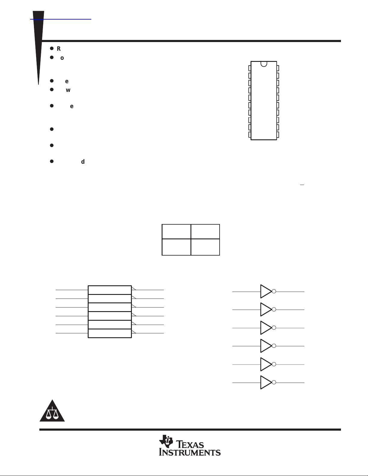
DW PACKAGE
(TOP VIEW)
1Y
1
2Y
2
3Y
3
GND
GND
GND
GND
4
5
6
7
4Y
8
9
5Y
10
6Y
NC – No internal connection
20
19
18
17
16
15
14
13
12
11
1A
2A
3A
NC
V
V
NC
4A
5A
6A
CC
CC
description
The CDC203 contains six independent inverters. The device performs the Boolean function Y = A. It is designed
specifically for applications requiring low skew between switching outputs.
The CDC203 is characterized for operation from 25°C to 70°C.
FUNCTION TABLE
INPUT
A
H L
L H
OUTPUT
Y
logic symbol
20
1A 1Y
19
2A 2Y
18
3A 3Y
13
4A 4Y
12
5A 5Y
11
6A
†
This symbol is in accordance with ANSI/IEEE Std 91-1984
and IEC Publication 617-12.
EPIC is a trademark of Texas Instruments Incorporated.
PRODUCTION DATA information is current as of publication date.
Products conform to specifications per the terms of Texas Instruments
standard warranty. Production processing does not necessarily include
testing of all parameters.
†
1
10
Please be aware that an important notice concerning availability, standard warranty, and use in critical applications of
Texas Instruments semiconductor products and disclaimers thereto appears at the end of this data sheet.
logic diagram (positive logic)
1
2
3
8
9
6Y
1A
2A
3A
4A
5A
6A
20
19
18
13
12
11
Copyright 1995, Texas Instruments Incorporated
10
1
1Y
2
2Y
3
3Y
8
4Y
9
5Y
6Y
POST OFFICE BOX 655303 • DALLAS, TEXAS 75265
1
CDC203
VIHHigh-level input voltage
V
VILLow-level input voltage
V
IOHHigh-level output current
mA
IOLLow-level output current
mA
3.3-V HEX INVERTER/CLOCK DRIVER
SCAS324A – OCTOBER 1989 – REVISED NOVEMBER 1995
absolute maximum ratings over operating free-air temperature range (unless otherwise noted)
Supply voltage range, VCC –0.5 V to 7 V. . . . . . . . . . . . . . . . . . . . . . . . . . . . . . . . . . . . . . . . . . . . . . . . . . . . . . . . . .
Input voltage range, VI (see Note 1) –0.5 V to VCC + 0.5 V. . . . . . . . . . . . . . . . . . . . . . . . . . . . . . . . . . . . . . . . . .
Output voltage range, VO (see Note 1) –0.5 V to VCC + 0.5 V. . . . . . . . . . . . . . . . . . . . . . . . . . . . . . . . . . . . . . .
Input clamp current, IIK (VI < 0 or VI > VCC) ±20 mA. . . . . . . . . . . . . . . . . . . . . . . . . . . . . . . . . . . . . . . . . . . . . . .
Output clamp current, IOK (VO < 0 or VO > VCC) ±50 mA. . . . . . . . . . . . . . . . . . . . . . . . . . . . . . . . . . . . . . . . . . .
Continuous output current, I
(VO = 0 to VCC) ±50 mA. . . . . . . . . . . . . . . . . . . . . . . . . . . . . . . . . . . . . . . . . . . . .
O
Continuous current through VCC or GND ±150 mA. . . . . . . . . . . . . . . . . . . . . . . . . . . . . . . . . . . . . . . . . . . . . . . . .
Maximum power dissipation at TA = 55°C (in still air) (see Note 2) 1.6 W. . . . . . . . . . . . . . . . . . . . . . . . . . . . . .
Storage temperature range, T
†
Stresses beyond those listed under “absolute maximum ratings” may cause permanent damage to the device. These are stress ratings only, and
functional operation of the device at these or any other conditions beyond those indicated under “recommended operating conditions” is not
implied. Exposure to absolute-maximum-rated conditions for extended periods may affect device reliability.
NOTES: 1. The input and output negative-voltage ratings may be exceeded if the input and output clamp-current ratings are observed.
2. The maximum package power dissipation is calculated using a junction temperature of 150°C and a board trace length of 750 mils.
For more information, refer to the
Data Book
, literature number SCBD002B.
–65°C to 150°C. . . . . . . . . . . . . . . . . . . . . . . . . . . . . . . . . . . . . . . . . . . . . . . . . .
stg
Package Thermal Considerations
application note in the 1994
ABT Advanced BiCMOS T echnology
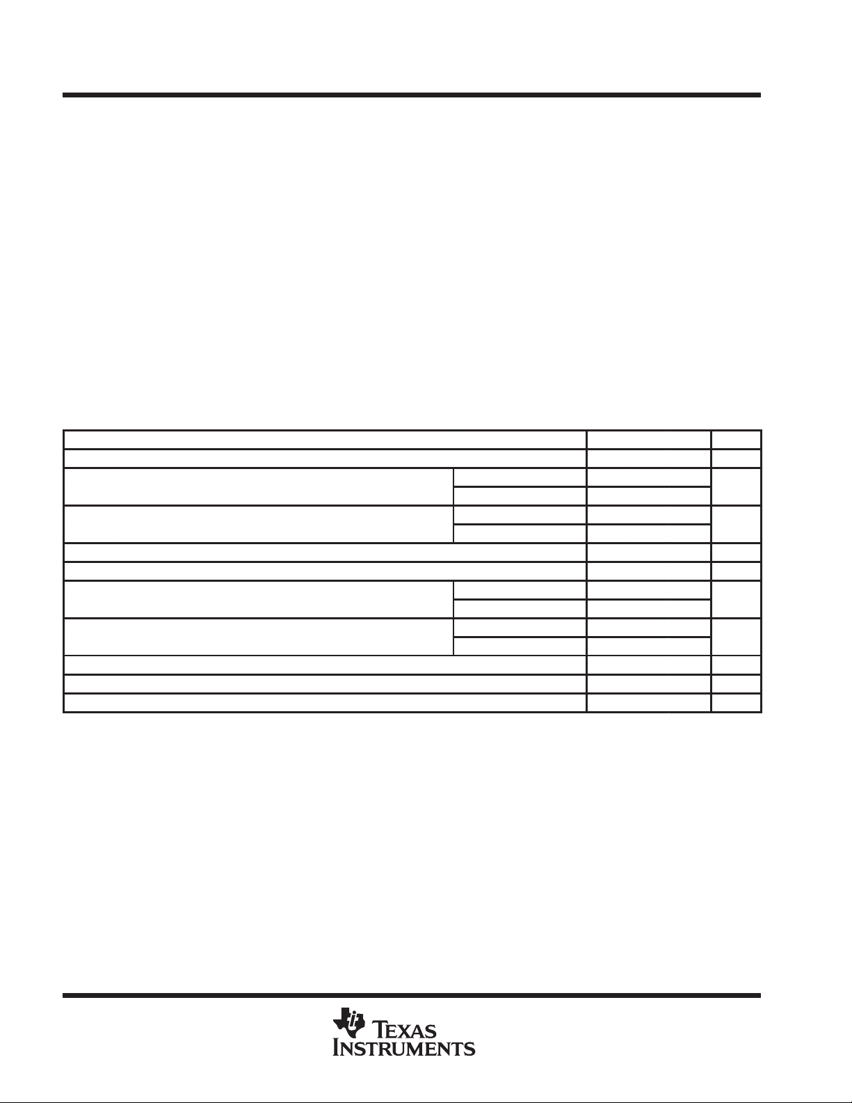
recommended operating conditions
MIN NOM MAX UNIT
V
CC
V
I
V
O
∆t/∆v Input transition rise or fall rate 0 10 ns/V
f
clock
T
A
Supply voltage 3 3.3 3.6 V
p
p
Input voltage 0 V
Output voltage 0 V
p
p
Input clock frequency 40 MHz
Operating free-air temperature 25 70 °C
VCC = 3 V 2.1
VCC = 3.6 V 2.5
VCC = 3 V 0.9
VCC = 3.6 V 1.1
CC
CC
VCC = 3 V –12
VCC = 3.6 V –12
VCC = 3 V 12
VCC = 3.6 V 12
V
V
†
2
POST OFFICE BOX 655303 • DALLAS, TEXAS 75265
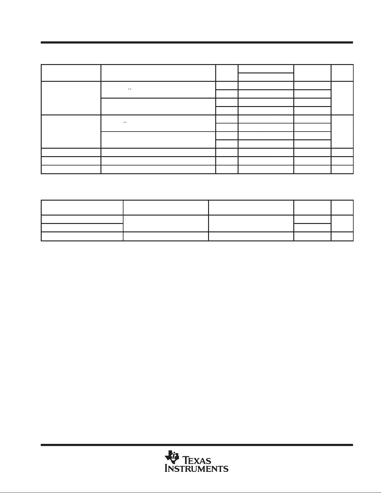
PARAMETER
TEST CONDITIONS
V
MIN
MAX
UNIT
I
A
V
V
I
mA
I
A
V
V
I
mA
A
Y
ns
CDC203
3.3-V HEX INVERTER/CLOCK DRIVER
SCAS324A – OCTOBER 1989 – REVISED NOVEMBER 1995
electrical characteristics over recommended operating free-air temperature range (unless
otherwise noted)
CC
3 V 2.9 2.9
3.6 V 3.5 3.5
3 V 2.58 2.48
3.6 V 3.18 3.08
3 V 0.1 0.1
3.6 V 0.1 0.1
3 V 0.36 0.44
3.6 V 0.36 0.44
I
I
C
OH
OL
I
CC
i
= –50 µ
OH
= –12
OH
= 50 µ
OL
= 12
OL
VI = VCC or GND 3.6 V ±0.1 ±1 µA
VI = VCC or GND, IO = 0 3.6 V 4 40 µA
VI = VCC or GND 3.3 V 4 pF
switching characteristics over recommended operating free-air temperature range,
= 3.3 V ± 0.3 V (see Note 3 and Figures 1 and 2)
V
CC
PARAMETER
t
PLH
t
PHL
t
sk(o)
NOTE 3: All specifications are valid only for all outputs switching in phase simultaneously.
FROM
(INPUT)
A Y 0.7 ns
TA = 25°C
MIN TYP MAX
TO
(OUTPUT)
MIN MAX UNIT
3.5 6.1
3.5 6.1
POST OFFICE BOX 655303 • DALLAS, TEXAS 75265
3
CDC203
3.3-V HEX INVERTER/CLOCK DRIVER
SCAS324A – OCTOBER 1989 – REVISED NOVEMBER 1995
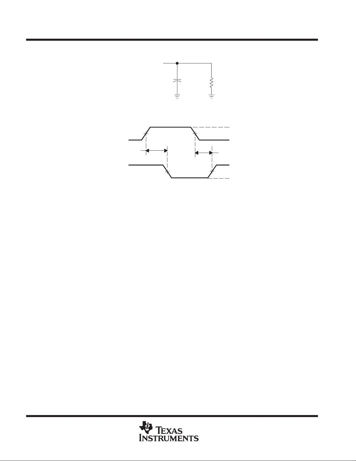
PARAMETER MEASUREMENT INFORMATION
From Output
Under Test
Input
(see Note B)
t
PLH
Output
NOTES: A. CL includes probe and jig capacitance.
B. Input pulses are supplied by generators having the following characteristics: PRR ≤ 10 MHz, ZO = 50 Ω, tr = 3 ns, tf = 3 ns.
C. The outputs are measured one at a time with one input transition per measurement.
Figure 1. Load Circuit and Voltage Waveforms
CL = 30 pF
(see Note A)
LOAD CIRCUIT
50% 50%
50% V
VOLTAGE WAVEFORMS
PROPAGATION DELAY TIMES
500 Ω
CC
t
PHL
50% V
V
0 V
V
CC
V
CC
OH
OL
4
POST OFFICE BOX 655303 • DALLAS, TEXAS 75265

CDC203
3.3-V HEX INVERTER/CLOCK DRIVER
SCAS324A – OCTOBER 1989 – REVISED NOVEMBER 1995
PARAMETER MEASUREMENT INFORMATION
1A–6A
Y1
Y2
Y3
Y4
Y5
t
PLH1
t
PLH2
t
PLH3
t
PLH4
50%
50%
50%
50%
50%
50%50%
50%
t
PHL1
50%
t
PHL2
50%
t
PHL3
50%
t
PHL4
50%
t
PLH5
Y6
t
PLH6
NOTE A: Output skew, t
– The difference between the fastest and slowest of t
– The difference between the fastest and slowest of t
50%
, is calculated as the greater of:
sk(o)
Figure 2. Waveforms for Calculation of t
(n = 1, 2,..., 6)
PLHn
(n = 1, 2,..., 6)
PHLn
sk(o)
50%
t
PHL5
t
PHL6
POST OFFICE BOX 655303 • DALLAS, TEXAS 75265
5

IMPORTANT NOTICE
T exas Instruments and its subsidiaries (TI) reserve the right to make changes to their products or to discontinue
any product or service without notice, and advise customers to obtain the latest version of relevant information
to verify, before placing orders, that information being relied on is current and complete. All products are sold
subject to the terms and conditions of sale supplied at the time of order acknowledgement, including those
pertaining to warranty, patent infringement, and limitation of liability.
TI warrants performance of its semiconductor products to the specifications applicable at the time of sale in
accordance with TI’s standard warranty. Testing and other quality control techniques are utilized to the extent
TI deems necessary to support this warranty . Specific testing of all parameters of each device is not necessarily
performed, except those mandated by government requirements.
CERTAIN APPLICATIONS USING SEMICONDUCTOR PRODUCTS MAY INVOLVE POTENTIAL RISKS OF
DEATH, PERSONAL INJURY, OR SEVERE PROPERTY OR ENVIRONMENTAL DAMAGE (“CRITICAL
APPLICATIONS”). TI SEMICONDUCTOR PRODUCTS ARE NOT DESIGNED, AUTHORIZED, OR
WARRANTED TO BE SUITABLE FOR USE IN LIFE-SUPPORT DEVICES OR SYSTEMS OR OTHER
CRITICAL APPLICA TIONS. INCLUSION OF TI PRODUCTS IN SUCH APPLICATIONS IS UNDERST OOD TO
BE FULLY AT THE CUSTOMER’S RISK.
In order to minimize risks associated with the customer’s applications, adequate design and operating
safeguards must be provided by the customer to minimize inherent or procedural hazards.
TI assumes no liability for applications assistance or customer product design. TI does not warrant or represent
that any license, either express or implied, is granted under any patent right, copyright, mask work right, or other
intellectual property right of TI covering or relating to any combination, machine, or process in which such
semiconductor products or services might be or are used. TI’s publication of information regarding any third
party’s products or services does not constitute TI’s approval, warranty or endorsement thereof.
Copyright 1998, Texas Instruments Incorporated
 Loading...