

Page 1
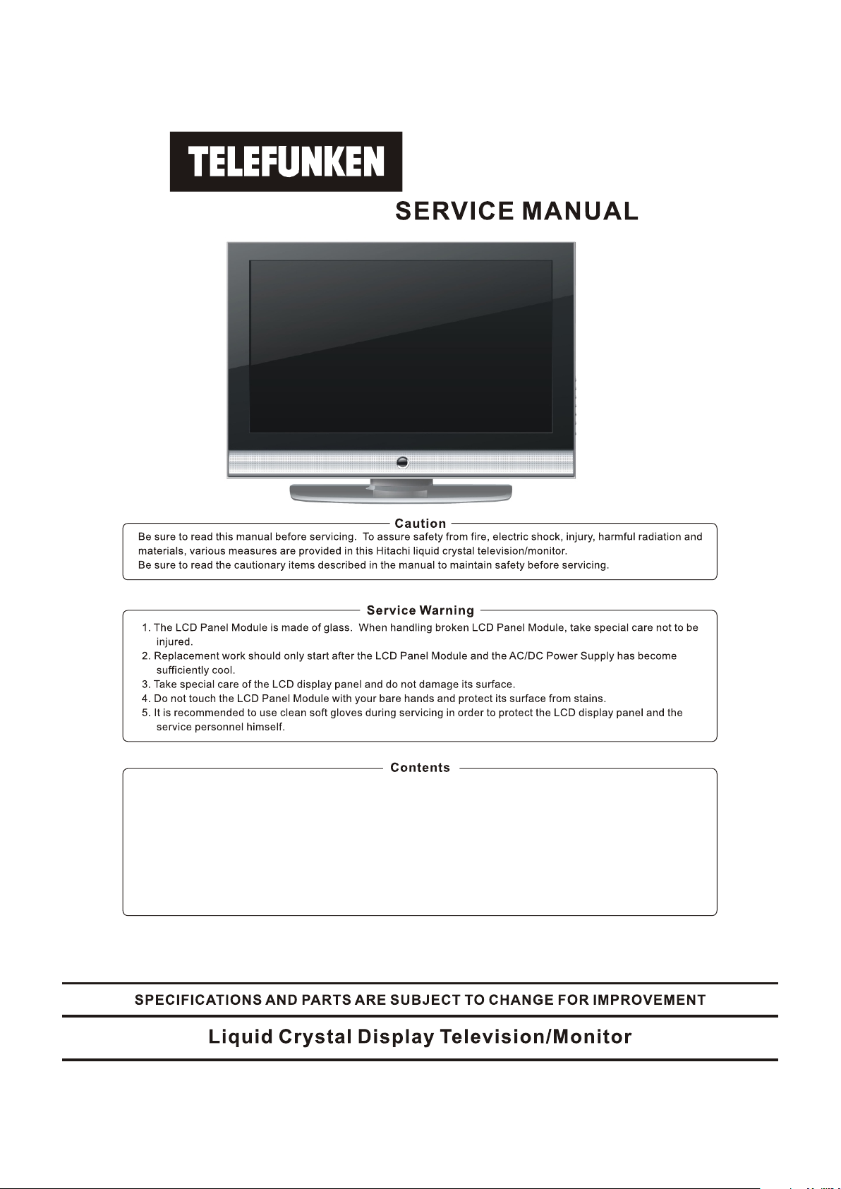
TF32K82A
TF37A82H
.Safety No ti ce 2 . Printed C ir cuit Bo ar d 31
.Display M od es . Block Dia gr am 34
2
.Specifi ca tions 4 .Wiring Dia gr am 35
.Locatio n an d Funct io n of
Control s 6 . Explode d View an d Me chanica l Pa rts 36
.Install at ion and c on necting 8 . I cs f uncti on d escript io n 39
. Schemti c Di agram s 15
. Parts Lis t( Fo r Re fe rence O nl y) 55
Page 2
COMPONENT VIDEO (YPbPr) INPUT
Mode Resolution
576i 576
480i 480
576p
480p
1080i/50
1080i/60
720p/60
576
480
1080
1080
720 44.96
Horizontal Frequency (K Hz) Vertical Frequency (Hz)
15.63
15.73
31.26
31.47
28.13
33.75
50.00
59.94/60.00
50.00
59.94/60.00
50.00
59.94/60.00
59.94/60.00
2
Page 3
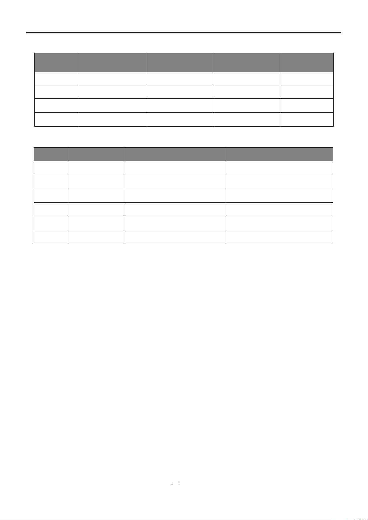
Display Modes
RGB INPUT
Resolution
640x480
800x600
1024x768
1280X768
HDMI INPUT
Mode Resolution
VGA
576p
1080i/50
1080i/60
720p/50
Horizontal
Frequency (KHz)
31.47 (N) 60.00 (N)
37.88 (P) 60.32(P)
38.36(N) 60.00(N)
64.00(P) 60.00(P)
640X480
720X576
1920X1080
1920X1080
1280X720
Vertical
Frequency (Hz)
Horizontal Frequency (K Hz) Vertical Frequency (Hz)
31.47
31.25
28.13
33.75
37.50
Frequency (MHz)
Pixel
25.18
40.00
65.00
108.00
Comment
DOS
VESA
VESA
VESA
59.94
50.00
50.00
60.00
50.00
720p/60
● Modes, which are not listed in the above table, may not be supported. For an optimal picture is
recommended to choose a mode listed in the table.
● The incoming display modes compatible with WINDOWS as shown in the table above.
● Sometimes, the image may be disrupted due to the frequency standard from the VGA card.
However, this is not an error. You may improve this situation by activating the automatic
adjustment or by manually changing the phase and the clock settings in the menu.
● To extend the service life of the product, we recommend that you use your computer’s power
management function.
1280X720
45.00
60.00
3
Page 4

Specifications
LCD Panel
Size
Display size
Pixel Pitch
View Angle
Frequency
Horizontal
Vertical
Display color
Display Resolution
Maximum Mode
Optimum Mode
Input Source
Sync.
Video Signal
RGB Signal
TV
Color System
Sound System
Video
Color System
Video Format
Power Supply
Input
Power Consumption
Working
Standby
Environmental Considerations
Operating Temperature
Operating Humidity
32" Diagonal
697.68(H) X 392.26 (V) mm
0.51075(H) X 0.51075 (V) mm
178 °/178°(H/V)
30~80KHz
56~60Hz
16.7M colors
1280 X 768 @ 60Hz
1280 X 768 @ 60Hz
H/V separate, TTL, P. or N.
1Vp-p @ 75 ohm
0.7 Vp-p @ 75 ohm
PAL/SECAM
BG, DK, I, L
PAL/SECAM/NTSC
CVBS, S-VHS, RGB
AC 100~240V, 50/60Hz
165W
< 3W
10℃ ~ 40 ℃(50°F ~ 104°F)
10% ~ 80%
37” Diagonal
819.6(H) X 460.8 (V) mm
0.6(H) X 0.6 (V) mm
178 °/178°(H/V)
30~80KHz
56~60Hz
16.7M colors
1280 X 768 @ 60Hz
1280 X 768 @ 60Hz
H/V separate, TTL, P. or N.
1Vp-p @ 75 ohm
0.7 Vp-p @ 75 ohm
PAL/SECAM
BG, DK, I, L
PAL/SECAM/NTSC
CVBS, S-VHS, RGB
AC 100~240V, 50/60Hz
200W
< 3W
10℃ ~ 40 ℃(50°F ~ 104°F)
10% ~ 80%
Audio Characteristics
Audio Input
Audio Input (PC)
Frequency
Response
Dimension ( WXDXH) mm
Without Stand
With Stand
Weight (Kg)
Net Weight
Gross Weight
Note:
● Design and specifications are subject to change without notice.
● Weight and dimensions shown are approximate values only.
RCA Jack (L, R), 0.5Vrms (-9dB)
RCA Jack (L, R), 0.5Vrms (-9dB)
RF: 100Hz~12KHz (at ± 3dB)
A/V: 100Hz~13KHz (at ± 3dB)
796X114X546
796X233X582
15.2
18.2
4
RCA Jack (L, R), 0.5Vrms (-9dB)
RCA Jack (L, R), 0.5Vrms (-9dB)
RF: 100Hz~12KHz (at ± 3dB)
A/V: 100Hz~13KHz (at ± 3dB)
947X126X644
947X310X710
23.5
27
Page 5
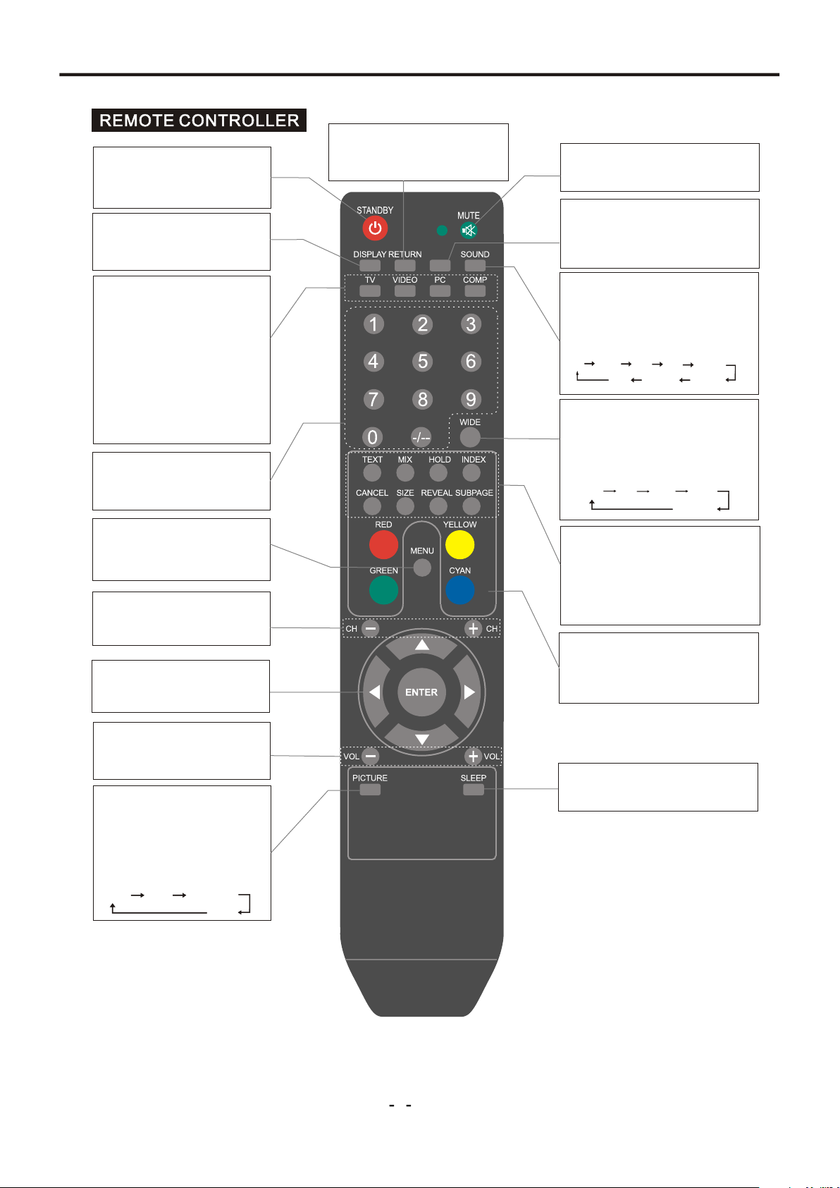
Location and Function of Controls
RETURN
STANDBY
Switch on the LCD TV when at
standby mode or vice versa.
DISPLAY
Display the source and channel
information.
INPUT SOURCE SELECT
TV button
Select the TV mode.
VIDEO button
Select a mode among AV,
S-Video and SCART.
PC button
Select the VGA and HDMI mode.
COMP button
Select the YPbPr mode.
PROGRAM SELECT
Press these buttons to select
a TV program directly.
MENU SELECT
Enter or exit from the OSD
menu.
CH+/CH-
Select channel in ascending or
descending order.
p q t u and ENTER
select menu items and adjust
menu values.
VOL+/VOL-
Press to increase or decrease
volume.
PICTURE MODE
You may recall the picture
mode by pressing this button.
Each time pressed, picture
mode is changed in following
sequence:
Sport Vivid Hi-Bright
User
Return to previously selected
program number.
NICAM
MUTE
Switch the sound on or off.
NICAM
Switch between NICAM Stereo,
NICAM DUAL1,NICAM DUAL2,
NICAM Mono or Mono.
EQ MODE
You may recall the equalizer mode
by pressing this button. Each time
pressed, EQ mode is changed in
following sequence.
Off Rock Pop Live
Soft
Classic
Dance
Techno
DISPLAY MODE
You may recall the display mode
by pressing this button. Each time
pressed, display mode is changed
in following sequence.
Full
4:3 16:9
TELETEXT
Auto
Normal
These buttons are used for
certain models with Teletext
functions. For further details,
refer to “TELETEXT
FUNCTION” section.
COLOR BUTTONS
These buttons are used for program
editing function. For further details,
refer to ‘‘Program Edit ’’.
SLEEP
To select the sleep time.
Note:
the prompt message “Invalid Key” will appear if you press a button for a function that is not
available.
5
Page 6
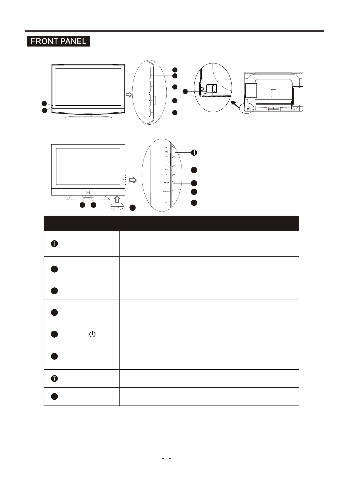
Location and Function of Controls
TF32K82A:
7
6
TF37A82H:
ItemItem
6
7
Button NameButton Name
INPUT
+
_
4
3
1
8
2
5
2
3
4
5
8
DescriptionDescription
VOL +/-
2
3
4
CHÚ/ÙCHÚ Ù
MENU
SOURCE/INPUT
5
Power Indicator
6
Remote Sensor
Main Power Switch
8
Increase or decrease the volume.
Adjust the values of the selected menu item in the OSD menu.
When you are watching the TV program, press these buttons
to select channel in ascending or descending order.
Select the upper or lower menu item in the OSD menu.
Enter or exit from the menu.
Select an input signal between TV, AV, S-Video, SCART,YPbPr,
HDMI and VGA.
Switch on the LCD TV when in standby mode or vice versa.
Illuminates red in standby mode.
Illuminates green when the LCD TV is switched on.
Infrared sensor for the remote control.
Switch on/off the LCD TV.
Note:
If there is no signal input from VGA/HDMI for 1 minute, or no signal input from other video source
(the blue background should be set to On) for over 15 minutes, the LCD TV will switch to standby
automatically. The power indicator will light up in red.
6
Page 7

Installation and Connecting
1
AC Input Socket
1
HDMI Input Connector
2
VGA Input Terminal
3
4
SCART Connector
YPbPr Component Video Input Terminals
5
6
AV Out Terminals
2
3
4
SCART
5
Y Pb Pr
AV OUT VID EO L R
6
7
VIDEO -AUDI O IN
L R
YPbPr -AUDI O IN
L R
9
8
10
11
LINE I N
13
12
Video-Audio Input Terminals
7
YPbPr-Audio Input Terminals
8
Video Input Terminal
9
10
S-VIDEO Terminal
LINE IN (VGA Audio) Terminal
11
Headphone Output Terminal
12
RF Input Socket
13
7
Page 8
8
Page 9
9
Page 10
10
Page 11

11
Page 12
12
Page 13

13
Page 14
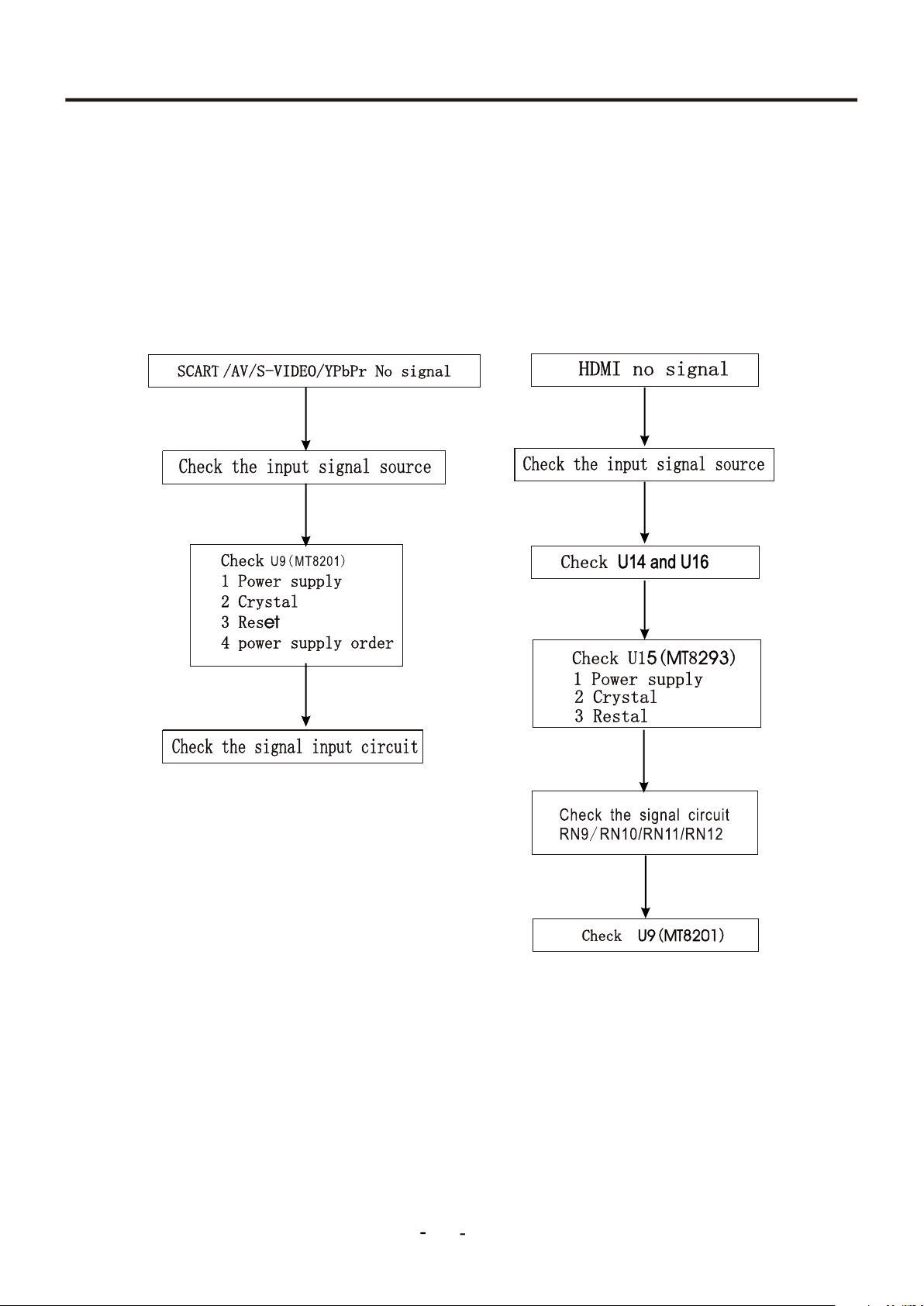
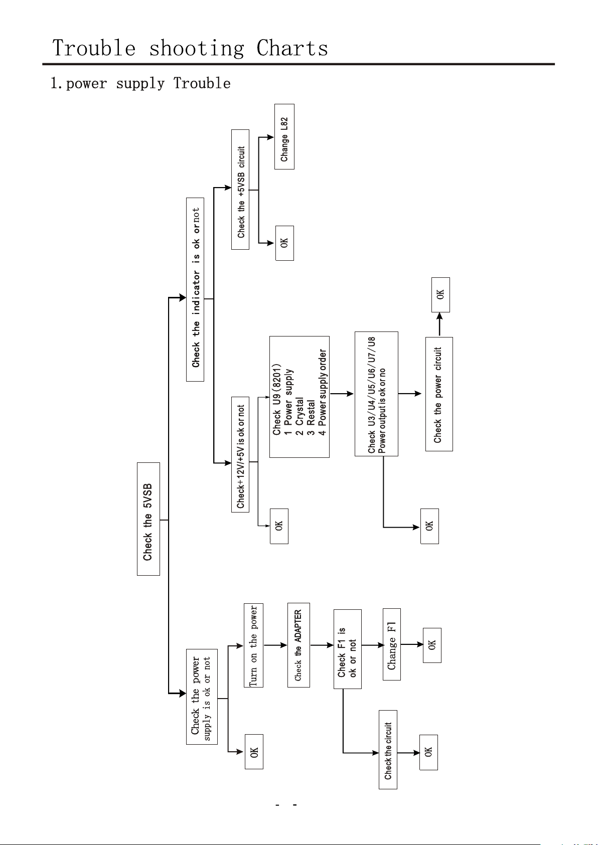
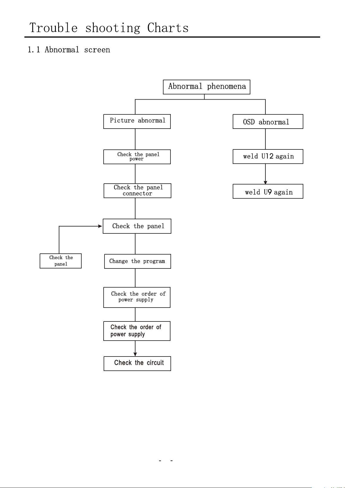
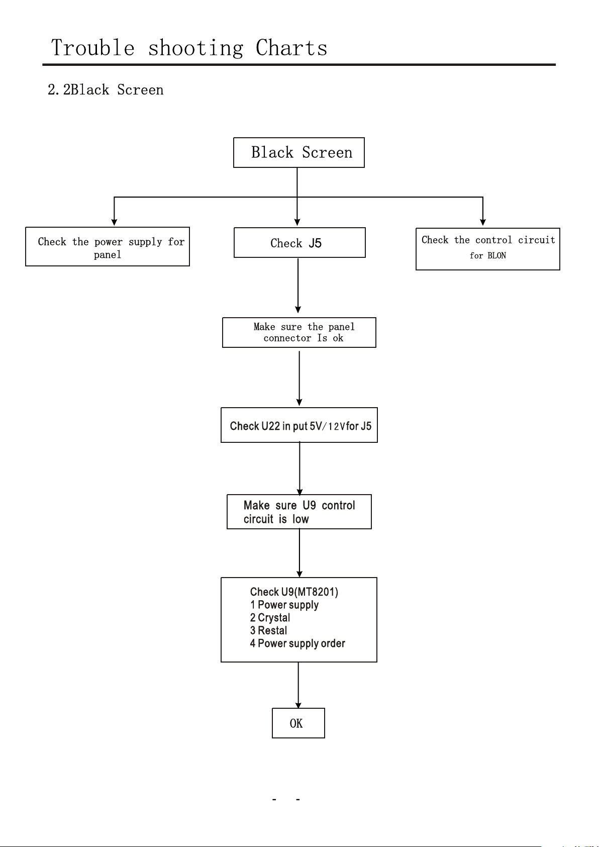
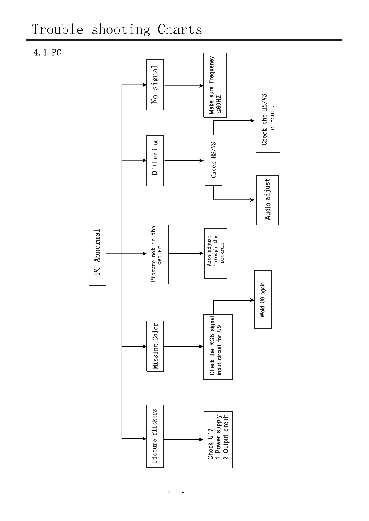
Trouble shooting Charts
4.3 No signal4.3 No signal
14
Page 15
Schemtic Diagrams
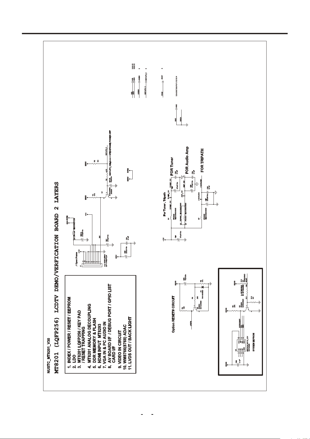
01.INDEX/ POWER/RESET/EEPROM
15
Figure1-1.1DRIVE Schematic Circuit
Page 16
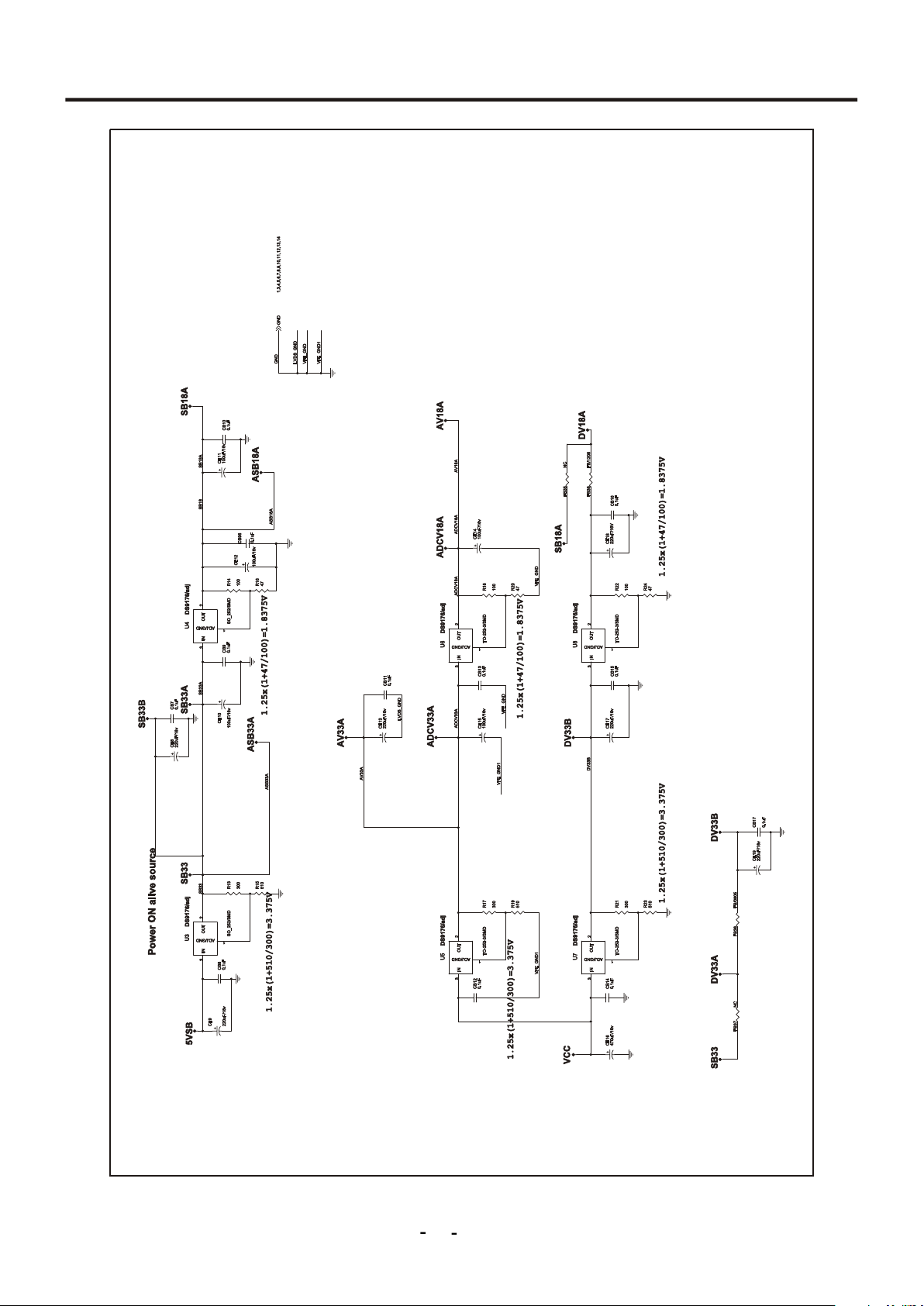
Schemtic Diagrams
02.POWER
16
Figure1-1.2DRIVE Schematic Circuit
Page 17
Schemtic Diagrams
03.MT8201/LQFP256
17
Figure1-1.3 DRIVE Schematic Circuit
Page 18
Schemtic Diagrams
04.MT8201 ANALOG DECOUPLING
18
Figure1-1.4 DRIVE Schematic Circuit
Page 19
Schemtic Diagrams
05.SDRAM MEMORY&FLASH
19
Figure1-1.5 DRIVE Schematic Circuit
Page 20

Schemtic Diagrams
06.HDMI INPUT-MT8293
20
Figure1-1.6 DRIVE Schematic Circuit
Page 21

Schemtic Diagrams
07.VGA IN&PC AUDIO IN
21
Figure1-1.7 DRIVE Schematic Circuit
Page 22

Schemtic Diagrams
08.AUDIO/ VIDEO IN CIRCUIT
22
Figure1-1.8 DRIVE Schematic Circuit
Page 23

Schemtic Diagrams
09.AUDIO Wm8776 ADAC
23
Figure1-1.9 DRIVE Schematic Circuit
Page 24

Schemtic Diagrams
10.LVDS
24
Figure1-1.10 DRIVE Schematic Circuit
Page 25

Schemtic Diagrams
11. AV/YPBPR CIRCUIT
25
Figure1-1.11DRIVE Schematic Circuit
Page 26

Schemtic Diagrams
12.TUNER
26
Figure1-1.12DRIVE Schematic Circuit
Page 27

Schemtic Diagrams
13.SCART
27
Figure1-13 DRIVE Schematic Circuit
Page 28

Schemtic Diagrams
14. AUDIO_AMP_TFA9843
LOUT
FB12 BEAD/SMD/0805FB12 BEAD/SMD/0805
FB11 BEAD/SMD/0805FB11 BEAD/SMD/0805
+
+
CE82 1000uF/35v +CE82 1000uF/35v
CE91 1000uF/35v +CE91 1000uF/35v
VCC_24V
8
2
T
U
O
R
c
c
V
9
N
N
I
I
R
L
4
1
TPA9843BJTPA9843BJ
CB91 220nFCB91 220nF
R44
47k
R44
47k
0
R2690R269
CE61
CE61
1000uF/35v
1000uF/35v
+
+
C114
C114
0.1uF
0.1uF
VCC_24V
8
6
5
D
D7D
0805
0805
FB9
FB9
U26/NC
U26/NC
S
S1S
2
FB10
FB10
FB/0805/NC
FB/0805/NC
D93
D93
新
更
IN5404
IN5404
日
D92
D92
12
月
4
IN5404
IN5404
+24VAMP
1
2
J2
2x1 W/HOUSING
DIP2/W/H/P2.54J22x1 W/HOUSING
DIP2/W/H/P2.54
T
U
O
L
D
N
G
5
E
D
V
R
O
I
M
C
SV
7
3
6
CB90 220nFCB90 220nF
R43
47k
R43
47k
R135 10KR135 10K
R270 0R270 0
CE20
220uF/25v+CE20
220uF/25v
+
CE81 22uF/25v
CE81 22uF/25v
+
+
R54
100
R54
100
Q21
2N3904
Q21
2N3904
3 2
1
新
更
日
R55 4.7KR55 4.7K
12
月
4
R287
10K
R287
10K
D89
D89
Q22A
2N3406
Q22A
2N3406
D/SMD/1N4148
D/SMD/1N4148
新
D
更
日
A
A
5
5
12
3
3
4
4
9
9
G
M
M
月
E
E
4
C
C
3
4
Q35
2N3904
Q35
2N3904
SOT23/SMD
SOT23/SMD
R54
10k
R54
10k
R413
R413
100k
100k
J3
J3
123
4
ROUT
LOUT
R140100K R140100K
+
+
CE93 100uF/25v
CE93 100uF/25v
3 2
1
2k
R4142kR414
GPIO_SDA1
4x1 W/HOUSING
4x1 W/HOUSING
DIP4/W/H/P2.0
DIP4/W/H/P2.0
GPIO_SDA1 9
LO = > LVDS POWER ON
GPIO_SDA1
ADC_IN3 3
SPOUTR 9
SPOUTL 9
A_MUTE 9
GND 1,2,3,4,5,6,7,8,9,10,11,12,14
A_MUTE
ADC_IN3
SPOUTR
SPOUTL
Figure1-13 DRIVE Schematic Circuit
HI = > LVDS POWER OFF
C115NCC115
NC
C116NCC116
NC
VCC_24V
SPOUTL
SPOUTR ROUT
4
D88 D/SMD/1N4148D88 D/SMD/1N4148
R211 10KR211 10K
4.7k
4.7k
R41
R41
+5VSB +5V
ADC_IN3
12V
D90 D/SMD/1N4148D90 D/SMD/1N4148
R1290R129
0
R2050R205
0
R1370R137
0
28
Page 29

Schemtic Diagrams
S_VIDEO_IN
VIDEO IN
TUNER CVBS IN
SC0 MT8201PIN166 MT8202PIN F26
CVBS0 MT8201PIN173 MT8202PIN D25
CVBS1 MT8201PIN172 MT8202PIN D26
CVBS2 MT8201PIN171 MT8202PIN E26
SY0 MT8201PIN167 MT8202PIN F25
CVBS3 MT8201PIN170 MT8202PIN E25
SY1 MT8201PIN165 MT8202PIN G25
Tuner
VIDEO_In
AVIn_R
SVIn_R
AVIn_L
SVIn_L
Pr_IN
Pb_IN
SC1 MT8201PIN164 MT8202PIN G26
Y_IN
Earphone
IN
PC Audio
SVideoIn
YPbPr_L YPbPr_R
L OUT
VideoOut R OUT
VIDEO1_In
AVIn1_R
SVIn_R
AVIn1_L
SVIn_L
Pr1_IN
Pb1_IN
Y1_IN
Tuner
Earphone
IN
PC Audio
S-Video_In
YPbPr1_L YPbPr1_R
R OUT
L OUT
Video_Out
VIDEO IN1
SCART1_PIN20 CVBS_IN/SVIDEO_Y
SCART1_PIN15 SVIDEO_C/R_IN
PR0
SCART2_PIN15 SVIDEO_C/R_IN
SCART2_PIN20 CVBS_IN/SVIDEO_Y
PR1
SCART/YPbPr
SCART
Pb2_IN Pr2_IN
YPbPr1 AND YPbPr2
Y2_IN
VGA
HDMI
Europe
YPbPr2_R
AVIn2_R
YPbPr2_L
AVIn2_L
Video2_ IN
VGA
HDMI
China
America
Figure1-14 DRIVE Schematic Circuit
29
Page 30

Schemtic Diagrams
30
Figure1-1CONTROL KEYS Schematic Circuit
Page 31

Printed Circuit Board
31
Figure2- 1.1 .DRIVE Board(Top Side)
Page 32

Printed Circuit Board
32
Figure2- 1.2 .DRIVE Board(Bottom Side)
Page 33

Printed Circuit Board
33
Figure2-3.1 CONTROL KEYS Board(Top Side)
Page 34

Printed Circuit Board
34
Figure2-3.2 CONTROL KEYS Board(BOTTOM Side)
Page 35

Wiring Dirgram
Figu re 3-2 Wiring Dia gram
35
Page 36

Exploded View and Mechanical Parts List
TF32K82A
36
Page 37

Exploded View and Mechanical Parts List
TF37A82H
37
Page 38

Exploded View and Mechanical Parts List
TF37A82H
38
Page 39

Info rmati on of ICs
U18
39
Page 40

Info rmati on of ICs
U23
40
Page 41

Info rmati on of ICs
U9
41
Page 42

Info rmati on of ICs
U9
42
Page 43

Info rmati on of ICs
U9
43
Page 44

Info rmati on of ICs
U9
44
Page 45

Info rmati on of ICs
U9
45
Page 46

Info rmati on of ICs
U9
U19、U20
46
Page 47

Info rmati on of ICs
U10
47
Page 48

Info rmati on of ICs
U14
1~3
4
5
6
7
8
U15
48
Page 49

Info rmati on of ICs
U15
U16、U17
1~3
4
5
6
7
8
49
Page 50

Info rmati on of ICs
U2
50
Page 51

Info rmati on of ICs
U12
VDD
DQ0
VDDQ
DQ1
DQ2
VSSQ
DQ3
DQ4
VDDQ
DQ5
DQ6
VSSQ
DQ7
VDD
LDQM
/WE
/CAS
/RAS
/CS
Ba0
Ba1
A10
A0
A1
A2
A3
51
Page 52

Info rmati on of ICs
U12
VDD
VSS
A4
A5
A6
A7
A8
A9
A11
NC
CKE
CLK
UDQM
NC
VSS
52
Page 53

Info rmati on of ICs
U14
1~3
4
5
6
7
8
U15
53
Page 54

Info rmati on of ICs
U12
DQ8
VDDQ
DQ9
DQ10
VSSQ
DQ11
DQ12
49
50
51
52
53
54
U13
VDDQ
DQ13
DQ14
VSSQ
DQ15
VDD
1~3
4
5
6
7
8
U3、U5、U4、U7、U8
1
2
3
U22
1~3
4
5~8
GND Grou nd
VDS
VGS
VGS
VGS
VGS
S
Date -Source Vo ltage
Gate -Source Vo ltage
Gate -Source Vo ltage
Gate -Source Vo ltage
Gate -Source Vo ltage
Inpu t
G
D
Outp ut
54
Page 55

Parts List (For Reference Only) (TF32K82A)
FOR REFERENCE ONLY
The components shown in the remaining pages served as a reference only. It is not meant for ordering of
componesnts for servicing purposes.Do not quote any components from these lists.
ELECTRONIC COMMON PART ASSEMBLY(FOR FSP ADAPTER) (RoHS)
Item Part No. Description Location
1 E0002-001005R0 BATTERY R03P MERCURY-FREE (RoHS)
2 E0002-002022R0 TOROIDAL FERRITE T22.5*10*13.8 (RoHS)
2.0)
4.5 TO Φ
Φ
Φ4.0 (
3 E0002-103008R0
4 E3202-001036R1 JACK AC POWER SOCKET TU-301-A-A 3PIN 180° (RoHS)
SHRINKABLE TUBE S-901(FLAME-REDARDANT) 125
(RoHS)
℃VW-1
5 E3404-001027R2
6 E3405-001064R0
7 E3421-002263R1
8 E3421-002344R0
E3421-002387R0
9
10 E3421-002415R0
11 E3421-002416R0 WIRE ASSY TJC3-11Y/11Y/10Y/7Y UL2468#22 L=220/180/180mm 11P/11P/10P/7P (RoHS)
12 E3421-002417R0
13 E3421-004046R0 WIRE UL1672#18 L=380mm 1P BLUE (RoHS)
14 E3421-004047R0 WIRE UL1672#18 L=380mm 1P BROWN (RoHS)
15 E3421-006057R1
16 E3422-001020R0 WIRE AV RCA M*3/RCA M*3 S518-02-001 L=1500MM 3P (RoHS)
AC CORD VDE VH3.96-3Y
AC CORD EUROPEAN Y003+H05VV-F 3× 0.75mm
WIRE ASSY PH-4Y/ UL2468#22 L=800mm /400mm 2.0mm 4P(
WIRE ASSY PH-9Y/PH-5Y/PH-4Y UL2547#26 L=500/580mm 2.0mm/2.0mm/2.0mm
9P/5P/4P
WIRE ASSY PH-6Y/PH-5Y UL2547#28 L=700
WIRE ASSY TJC3-4Y/2Y UL2468#22 L=250mm 2.5/2.0mm 4P/2P
WIRE ASSY TJC3-10Y PH-14Y/3Y UL2468#22 L=530/230mm 2.5/2.5/2.0mm
14P/10P/3P (RoHS
WIRE ASSY 2.0-2X15P/JAE FI-X-30P(WITH LOCK) L=290mm 2.0mm/1.0mm 30/30p
(RoHS)
(
RoHS
)
)
Φ
4.2 3×0.75mm² 2.5A 640mm (RoHS)
2
+ST3 L= 2000mm (RoHS)
RoHS
mm 2.0mm/2.0mm 6P/5P (RoHS)
)
(RoHS
)
17 E4101-001017R0 PUSH BUTTON SWITCH KDC-A04-S 250VAC 10A (RoHS)
18 E5501-001051R0 ADAPTER VP192UG01-GP 5Vsb/0.5A 5V/4A 12V/2A 24V/5A 24V /1A (ROHS)
19
20 E6101-001096R2 TFT-LCD LC320WX3-SLE1 LG-PHILIPS(RoHS)
E5601-001039R1 SPEAKER 8OHM 15W YDT513-1A (RoHS)
-55-
Page 56

Parts List (For Reference Only) (TF37A82H)
FOR REFERENCE ONLY
The components shown in the remaining pages served as a reference only. It is not meant for ordering of
componesnts for servicing purposes.Do not quote any components from these lists.
ELECTRONIC COMMON PART ASSEMBLY(FOR FSP ADAPTER) (RoHS)
Item Part No. Description Location
1 E0002-002022R0 TOROIDAL FERRITE T22.5*10*13.8 (RoHS)
2 E0002-001005R0 BATTERY R03P MERCURY-FREE (RoHS)
1.0)
2.5 TO Φ
Φ
Φ2.0 (
3 E0002-103004R0
4 E0002-103008R0
5 E1302-003006R1 CAP EC NP V CD71-BP T05 1R0M 50DC 5×11 (RoHS)
6 E3202-001036R1 JACK AC POWER SOCKET TU-301-A-A 3PIN 180° (RoHS)
SHRINKABLE TUBE S-901(FLAME-REDARDANT) 125
(RoHS)
SHRINKABLE TUBE S-901(FLAME-REDARDANT) 125
(RoHS)
℃VW-1
℃
VW-1
Φ
4.0 (
Φ
4.5 TO
Φ
2.0)
7 E3404-001027R2
8 E3405-001064R0 AC CORD EUROPEAN Y003+H05VV-F 3× 0.75mm2 +ST3 L= 2000mm (RoHS)
9 E3421-002328R1 WIRE ASSY PH-4Y UL2468 #22 L=960/460mm 2.0mm/ 4P (RoHS)
10 E3421-002362R1
11
12 E3421-002480R0 WIRE ASSY TJC3-10Y PH-14Y/3Y UL2468#22 L=600/300mm 14P/10P/3P (RoHS)
13 E3421-002415R0
14 E3421-002416R0 WIRE ASSY TJC3-11Y/11Y/10Y/7Y UL2468#22 L=220/180/180mm 11P/11P/10P/7P (RoHS)
15 E3421-004045R0 WIRE 22# L=150mm RED/BLACK 2P (RoHS)
16 E3421-004046R0 WIRE UL1672#18 L=380mm 1P BLUE (RoHS)
17 E3421-004047R0 WIRE UL1672#18 L=380mm 1P BROWN (RoHS)
18 E3421-006057R1
19 E3422-001020R0 WIRE AV RCA M*3/RCA M*3 S518-02-001 L=1500MM 3P (RoHS)
E3421-002387R0
AC CORD VDE VH3.96-3Y Φ
WIRE ASSY PH-9Y/PH-5Y/PH-4Y UL2547#26 L=580/660mm 2.0mm/2.0mm/2.0mm
9P/5P/4P
WIRE ASSY PH-6Y/PH-5Y UL2547#28 L=
WIRE ASSY TJC3-4Y/2Y UL2468#22 L=250mm 2.5/2.0mm 4P/2P (
WIRE ASSY 2.0-2X15P/JAE FI-X-30P(WITH LOCK) L=290mm 2.0mm/1.0mm 30/30p
(RoHS)
(RoHS
)
4.2 3×0.75mm² 2.5A 640mm (RoHS)
700
mm 2.0mm/2.0mm 6P/5P (RoHS)
RoHS)
20 E4101-001018R0 SWITCH POWER KND3-B31 (RoHS)
21 E5501-001051R1 ADAPTER VP192UG01-GP 5Vsb/0.5A 5V/4A 12V/2A 24V/5A 24V /1A (ROHS)
22 E5601-001040R0 SPEAKER 8OHM 15W (RoHS)
23 E5601-001042R0 SPEAKER YDG50-1 8OHM 3W (RoHS)
24 E6101-001115R0 TFT-LCD LC370WX4-SLA1 LG-PHILIPS (RoHS)
-56-
Page 57

Parts List (For Reference Only) TF32K82A TF37A82H
FOR REFERENCE ONLY
The components shown in the remaining pages served as a reference only. It is not meant for ordering of
componesnts for servicing purposes.Do not quote any components from these lists.
DRIVE PCB ASSEMBLY (W/O AV YPRPB) (RoHS)
Item Part No. Description Location
1 E1101-001025R1 COIL FIX H AL0204S T52 220J (RoHS) L52 L20 L21
2 E1111-002019R1 COIL FIX CHIP CMI1608VBP 2R2M 0603 (RoHS)2.2uH L31 L32 L59 L62
3 E1111-003018R2 COIL FIX CHIP CMI2012VTP 1R8K 0805 (RoHS) L54 L53
FB1 FB2 FB3 FB4 FB6 FB7 FB8 L17
4 E1111-014004R1 FB FIX CHIP CBY160808UBP 190 0603 (ROHS)
5 E1111-015003R1 FB FIX CBY201209UBP 190 0805(ROHS) L22 FB5 L4 L8 FB22 FB38 L55
6 E1111-016001R2 FB FIX CHIP CBY321611UBP 190 1206(ROHS) L35 L37 L82 FB36
L18 L19 L23 FB23 L24 L25 L26 L27
L28 L29 L30 FB31 L33 FB33 L34 L57
L60 L63 L64 L65 L66 L67 L76 L77
L78 L79 L80 L81
7 E1112-001007R0 COIL FIX LBS7045-470MT 47uH 0.75A (RoHS) L56 L58
CE5 CE22 CE23 CE24 CE25 CE26
CE27 CE28 CE38 CE40 CE43 CE47
8 E1301-002001R1 CAP EC V CD11X-BP T05 100M 16DC 4×7 (RoHS)
9 E1301-002003R1 CAP EC V CD11X-BP T05 330M 16DC 5×7 (RoHS) CE86 CE108 CE111 CE115 CE119
10 E1301-002004R1 CAP EC V CD11X-BP T05 470M 16DC 5×7 (RoHS)
11 E1301-002005R1 CAP EC V CD11X-BP T05 101M 16DC 6.3×7 (RoHS)
12 E1301-002008R1 CAP EC V CD11X-BP T05 471M 16DC 8×12 (RoHS)
13 E1301-003003R1 CAP EC V CD11X-BP T05 220M 25DC 5×7 (RoHS) CE81
14 E1301-009001R1 CAP EC V CD11X-BP T05 221M 25DC 8×9 (RoHS) CE20
15 E1301-012015R1 CAP EC V CD11-BP T05 221M 16DC 6×12 (RoHS)
16 E1301-013010R1 CAP EC V CD11-BP T05 102M 25DC 12×20 (RoHS) CE82 CE91
17 E1301-014012R1 CAP EC V CD11-BP T05 102M 35DC 13x20 (ROHS) CE61
CE50 CE51 CE52 CE53 CE54 CE55
CE56 CE57 CE58 CE60 CE62 CE63
CE64 CE65 CE66 CE67 CE71 CE72
CE74 CE75 CE83 CE87 C98 CE136
CE21 CE36 CE37 CE41 CE70 CE122
CE126 CE128 CE135
CE8 CE10 CE11 CE12 CE14 CE15
CE17 CE18 CE19 CE33 CE34 CE35
CE76 CE88 CE100 CE123 CE127
CE1 CE3 CE4 CE73 CE77 CE85 CE89
CE92 CE97 CE114 CE134
CE2 CE9 CE13 CE16 CE29 CE30
CE32 CE42 CE44 CE45 CE46 CE68
CE69 CE78 CE84 CE90 CE95 CE101
18 E1301-020004R1 CAP EC V CD11 T05 101M 16DC 5×7(RoHS) CE93
19 E1321-230037R1 CAP POLYESTER FILM CL11 224J 100VDC (RoHS) CB90 CB91
20 E1326-001006R2 CAP CHIP CC41-CGNT NPO T06 5R0J 50DC 0603 (RoHS) C50 C53 C57 C58 C59
21 E1326-001011R2 CAP CHIP CC41-CGNT NPO T06 100J 50DC 0603 (RoHS) C185
22 E1326-001013R2 CAP CHIP CC41-CGNT NPO T06 150J 50DC 0603 (RoHS) C68 C74 C80 C87 C89 C93 C94 C95
-57-
Page 58

CB1 CB2 C4 CB5 CB6 CB7 CB8 CB9
R1 R45 R64 R88 R90 R121 R171 R180
Parts List (For Reference Only)
FOR REFERENCE ONLY
The components shown in the remaining pages served as a reference only. It is not meant for ordering of
componesnts for servicing purposes.Do not quote any components from these lists.
DRIVE PCB ASSEMBLY (W/O AV YPRPB) (RoHS)
Item Part No. Description Location
23 E1326-001014R2 CAP CHIP CC41-CGNT NPO T06 180J 50DC 0603 (RoHS) C2 C1 C46 C47
24 E1326-001018R2 CAP CHIP CC41-CGNT NPO T06 270J 50DC 0603 (RoHS) C143
25 E1326-001029R2 CAP CHIP CC41-CGNT NPO T06 151J 50DC 0603 (RoHS) C105 C103
26 E1326-001032R2 CAP CHIP CC41-CGNT NPO T06 221J 50DC 0603 (RoHS) C99 C101
27 E1326-001035R2 CAP CHIP CC41-CGNT NPO T06 331J 50DC 0603 (RoHS)
28 E1326-001040R2 CAP CHIP CC41-CGNT NPO T06 821J 50DC 0603 (RoHS) C106 C104
29 E1326-001057R2 CAP CER CHIP CC41-CGNT NPO 1R8J 50DC 0603 C91
30 E1326-003015R2 CAP CER CHIP CC41-BNT X7R T06 102K 50DC 0603 (RoHS)
31 E1326-003020R2 CAP CER CHIP CC41-BNT X7R T06 222K 50DC 0603 (RoHS) C100 C102
C65 C66 C71 C72 C77 C78 C83 C84
C149 C151 C145 C146
C36 C37 C38 C39 C40 C41 C42 C43
C44
32 E1326-003023R1 CAP CER CHIP CC41-BNB X7R T06 332K 50DC 0603 (RoHS) C3 C6 C8 C9 C10 C34 C35
C5 C23 C48 C60 C61 C107 C109 C111
33 E1326-003029R2 CAP CER CHIP CC41-BNT X7R T06 103K 50DC 0603 (RoHS)
34 E1326-003039R2 CAP CER CHIP CC41-BNT X7R 473K 50DC 0603 (RoHS) C63 C64 C69 C70 C75 C76 C81 C82
35 E1326-003051R2 CAP CER CHIP CC41-BNT X7R 472K 50DC 0603 (RoHS) C51 C62 C85
36 E1326-055029R2 CAP CER CHIP 0603F 104M500NB 104M 50D 0603 (ROHS)
37 E1326-064002R2 CAP CER CHIP CC41-0805E106Z T08 106Z 10DC 0805 (ROHS) C11 C20 C21 C24
38 E1326-105031R2 CAP CER CHIP CC41-FNT Y5V 105M 25DC 0603(ROHS)
39 E1326-106001R2 CAP CER CHIP 475Z 6.3DC 0603 (ROHS)
C112 C117 C118 C119 C120 C49 C52
C54 C67 C73 C79 C86 C88 C90 C92
C141 C142 C144
CB10 CB11 CB12 C12 CB13 CB14
CB15 CB16 CB17 CB18 CB19 CB20
CB21 CB22 C22 CB23 CB24 CB25
CB26 CB27 CB28 CB29 CB30 CB31
CB32 CB33 CB34 CB36 CB38 CB40
CB41 CB42 CB43 CB45 C45 CB46
CB47 CB48 CB49 CB50 CB51 CB52
CB53 CB54 CB55 CB56 CB57 CB58
CB59 CB60 CB61 CB62 CB63 CB64
CB65 CB66 CB67 CB68 CB69 CB70
CB71 CB72 CB73 CB74 CB75 CB76
CB77 CB78 CB79 CB80 CB81 CB82
CB83 CB84 CB85 CB86 CB87 CB88
CB89 CB93 CB94 CB95 CB96 CB98
CB99 CB100 CB101 CB107 CB109
C15 C17 C18 C32 C33 CB35 CB37
CB44 CB92 C96 C97 C148 C150
C13 C14 C16 C19 C25 C26 C27 C28
C29 C30 C31
40 E1503-321109R1 RES MOF H 2W S 430J T52 (RoHS) R5 R7
41 E1505-011003R2 RES CHIP RC-03KTP T06 1/10W 100J 0603 (RoHS)
42 E1505-011004R2 RES CHIP RC-03KTP T06 1/10W 101J 0603 (RoHS)
43 E1505-011005R2 RES CHIP RC-03KTP T06 1/10W 102J 0603 (RoHS)
R263 R301 R321 R329 R338 R358
R395
R14 R18 R22 R40 R42 R101 R103
R169 R176 R177 R179 R212
R181 R191 R259 R260 R340 R364
-58-
Page 59

Parts List (For Reference Only)
FOR REFERENCE ONLY
The components shown in the remaining pages served as a reference only. It is not meant for ordering of
componesnts for servicing purposes.Do not quote any components from these lists.
DRIVE PCB ASSEMBLY (W/O AV YPRPB) (RoHS)
Item Part No. Description Location
R4 R11 R34 R35 R51 R53 R54 R99 R100
R114 R115 R162 R172 R173 R178 R183
R186 R194 R208 R213 R214 R217 R218
44 E1505-011006R2 RES CHIP RC-03KTP T06 1/10W 103J 0603 (RoHS)
45 E1505-011007R2 RES CHIP RC-03KTP T06 1/10W 104J 0603 (RoHS)
46 E1505-011008R2 RES CHIP RC-03KBP T06 1/10W 105J 0603 (RoHS) R82 R25
47 E1505-011013R2 RES CHIP RC-03KTP T06 1/10W 111J 0603 (RoHS) R336 R243
R220 R221 R226 R227 R230 R231 R272
R273 R304 R327 R334 R335 R339 R356
R363 R371 R379 R381 R382 R242 R135
R287 R211 R206 R406
R148 R150 R153 R156 R157 R158
R159 R161 R184 R189 R203 R140
R413
48 E1505-011042R2 RES CHIP RC-03KBP T06 1/10W 153J 0603 (RoHS) R160 R170
49 E1505-011057R2 RES CHIP RC-03KTP T06 1/10W 180J 0603 (RoHS) R216 R222 R223
50 E1505-011059R2 RES CHIP RC-03KTP T06 1/10W 182J 0603 (RoHS) R258
51 E1505-011068R2 RES CHIP RC-03KBP T06 1/10W 202J 0603 (RoHS) R110 R113 R204 R380 R414
52 E1505-011069R2 RES CHIP RC-03KTP T06 1/10W 203J 0603 (RoHS) R9 R6
53 E1505-011075R2 RES CHIP RC-03KTP T06 1/10W 220J 0603 (RoHS) R58 R59
54 E1505-011076R2 RES CHIP RC-03KTP T06 1/10W 221J 0603 (RoHS) R262
55 E1505-011078R2 RES CHIP RC-03KTP T06 1/10W 223J 0603 (RoHS) R182 R190
56 E1505-011101R2 RES CHIP RC-03KTP T06 1/10W 301J 0603 (RoHS) R13 R17 R21
57 E1505-011108R2 RES CHIP RC-03KTP T06 1/10W 330J 0603 (RoHS)
58 E1505-011110R2 RES CHIP RC-03KTP T06 1/10W 332J 0603 (RoHS) R239 R298 R328 R347
59 E1505-011111R2 RES CHIP RC-03KTP T06 1/10W 333J 0603 (RoHS) R361 R322
60 E1505-011127R2 RES CHIP RC-03KTP T06 1/10W 393J 0603 (RoHS) R141 R142
61 E1505-011140R2 RES CHIP RC-03KTP T06 1/10W 470J 0603 (RoHS) R16 R20 R24
62 E1505-011141R2 RES CHIP RC-03KTP T06 1/10W 471J 0603 (RoHS) R397
63 E1505-011142R2 RES CHIP RC-03KTP T06 1/10W 472J 0603 (RoHS)
64 E1505-011143R2 RES CHIP RC-03KTP T06 1/10W 473J 0603 (RoHS)
65 E1505-011148R2 RES CHIP RC-03KTP T06 1/10W 510J 0603 (RoHS) R47 R48 R49 R50 R165 R175
R80 R267 R376 R377 R164 R166 R167 R168
R188 R196 R330 R240
R2 R37 R38 R41 R46 R55 R72 R87
R197 R210 R215 R383
R8 R43 R44 R67 R68 R144 R146 R147
R149 R192 R326 R370
66 E1505-011149R2 RES CHIP RC-03KTP T06 1/10W 511J 0603 (RoHS) R15 R19 R23 R109 R112
67 E1505-011150R2 RES CHIP RC-03KTP T06 1/10W 512J 0603 (RoHS) R163 R174 R187 R195
68 E1505-011151R2 RES CHIP RC-03KTP T06 1/10W 513J 0603 (RoHS) R154 R155
-59-
Page 60

)
Parts List (For Reference Only)
FOR REFERENCE ONLY
The components shown in the remaining pages served as a reference only. It is not meant for ordering of
componesnts for servicing purposes.Do not quote any components from these lists.
DRIVE PCB ASSEMBLY (W/O AV YPRPB) (RoHS)
Item Part No. Description Location
69 E1505-011156R2 RES CHIP RC-03KTP T06 1/10W 560J 0603 (RoHS) R219 R224 R225
70 E1505-011172R2 RES CHIP RC-03KTP T06 1/10W 680J 0603 (RoHS)
71 E1505-011180R2 RES CHIP RC-03KTP T06 1/10W 750J 0603 (RoHS)
72 E1505-011190R2 RES CHIP RC-03KTP T06 1/10W 822J 0603 (RoHS) R138
73 E1505-011202R2 RES CHIP RC-03KTP T06 1/10W 000 0603 (RoHS)
74 E1505-025003R1 RES CHIP RC-05KJT 1/8W 100J 0805 (RoHS) R143 R145
75 E1505-025202R1 RES CHIP RC-05KJT 1/8W 000 0805 (RoHS) FB9
76 E1510-001108R2 RES CHIP TFN RCML08WTP 1/16W 330J 0603×4 (RoHS) RN9 RN10 RN11 RN12
77 E2111-001015R1 TR PNP CHIP TC3906 SOT-23 TP (RoHS) Q9 Q22
78 E2112-001016R1 TR NPN CHIP TC3904 SOT-23 TP (RoHS)
79 E2115-001006R1 TR AP9435GM SINGLE P-CHANNEL MOSFET SO-8(RoHS) U22
R92 R97 R106 R120 R124 R128 R134
R136 R139
R93 R98 R107 R233 R237 R248 R249
R252 R253 R257 R264 R271 R302
R305 R306 R323 R324 R325
R26 R28 R30 R32 R39 R52 R57 L61 R61
R71 R73 R74 L74 R76 R77 R78 R79 R84
R85 R86 R89 R91 R95 R96 R102 R104
Q1 Q2 Q3 Q5 Q6 Q7 Q8 Q10 Q11 Q12
Q13 Q14 Q15 Q17 Q18 Q19 Q21 Q23
Q24 Q25 Q29 Q32 Q33 Q34 Q35
80 E2115-001022R0 SSS2N7002E N-CHANNEL ENHANCEMENT MODE MOSFET SOT23 (RoHS) QF3 QF4 QF5
81 E2301-001091R0
82 E2351-001176R0 IC AIC1084CE 5A LOW DROPOUT POSITIVE REGULATOR TO-252 (RoHS) U3 U5 U4 U6 U7 U8
83 E2351-001206R0 IC AF24BC02-SI(2K) 2-wire Serial EEPROM 8-pin SOIC (RoHS) U16 U17
84 E2351-001210R0 IC AZ1117H-1.8 (RoHS) U13
85 E2351-001222R0 IC MT8201 ADC+DECODER+SCALING+MCU LQFP-256 (RoHS) U9
86 E2351-001223R0 IC MT8293 HDMI PANELLINK RECEIVER LQFP128 (RoHS) U15
87 E2351-001225R0 IC WM8776 LQFP48 (RoHS) U18
88 E2351-001227R0 IC AT24C04N-10SI-2.7 4K(256X8) SERIAL EEPROM 8S1 (RoHS) U14
89 E2351-001237R0 IC AZ4558CM-E1 DUAL OPERATIONAL AMPLIFIER SOIC-8 (RoHS) U19 U20
91 E2354-001058R0 IC ES29LV800EB-70TG 8M FLASH MEMORY TSOP48 (RoHS) U10
92 E2354-001064R0 IC SDRAM M12L64164A-5TG TSOP-54(RoHS) U12
IC TFA9843J 2-CHANNEL AUDIO AMPLIFIER(SE:1W TO 20W RO BTL:4W TO 40W
DBS9P
U23
-60-
Page 61

Parts List (For Reference Only)
FOR REFERENCE ONLY
The components shown in the remaining pages served as a reference only. It is not meant for ordering of
componesnts for servicing purposes.Do not quote any components from these lists.
DRIVE PCB ASSEMBLY (W/O AV YPRPB) (RoHS)
Item Part No. Description Location
93 E2501-003021R1 DIODE SILICON H 1N5404 T52 DO-201AD BP (RoHS) D92 D93
94 E2502-001009R0 DIODE CHIP LL4148 (RoHS)
95 E2502-001014R0 MULTILAYER VARISTOR CHIP TYPE EZJZ1V270GA 0603 ESD
96 E3101-001002R1 PLUG PH-3A PIN HEADER (180°) 2.0mm 3P (RoHS) J12
97 E3101-001003R1 PLUG PH-4A PIN HEADER (180°) 2.0mm 4P (RoHS) J4 J3
98 E3101-001005R1 PLUG PH-6A PIN HEADER (180°) 2.0mm 6P (RoHS) J10
99 E3101-001008R1 PLUG PH-6A PIN HEADER (180°) 2.0mm 9P (RoHS) J11
100 E3101-002001R1 PLUG TJC3-11A PIN HEADER (180°) 2.5mm 2P (RoHS) J2
101 E3101-002010R1 PLUG TJC3-11A PIN HEADER (180°) 2.5mm 11P (RoHS) J1
102 E3101-015005R1 SOCKET PIN HEADER (180°) 2.0mm 2×15P (RoHS) J5
103 E3201-001090R1 SOCKET PIN SCART CS-2104 21P (RoHS) P9
104 E3201-001095R1 JACK PIN AV4-13W-070 W/R W/R 4P (RoHS) P6
D15 D16 D26 D27 D28 D29 D66 D11
D1 D88 D89 D90
D14 D17 D18 D19 D20 D21 D22 D23
D24 D25 D30 D31 D32 D33 D34 D35
D36 D37 D38 D39 D40 D41 D42 D44
D45 D46 D48 D49 D50 D51 D52 D53
D54 D55 D56 D57 D58 D60 D61 D62
D63 D64 D65
105 E3201-001125R1 SPEAKER JACK CK3-3.5-720 7P (RoHS) J13 J14
106 E3201-001126R2 D-sub 1152-015-201-000 3.08mm Footprint 15P (90°) (RoHS) P2
107 E3201-001137R1 JACK PIN AV6-11WD-550 G/B/R Y/W/R 6P (RoHS) P8
108 E3201-001138R1 JACK PIN AV-S+02B 4P/1P(RoHS) P5
109 E3202-001047R1 JACK HDMI RIGHT ANGLE HEADER ASSRMBLY E11001-04 (RoHS) P1
110 E3702-002143R3 MTK32H81 DRIVE PCB 293mmX142mm (RoHS)
111 E4301-001070R0 OSCILLATOR X' TAL HC-49US 27.000MHz (RoHS) Y1 Y2
112 E5401-001031R0 TUNER JS-6H2/121A25 PAL BG/DK/I SECAM L/L' XUGUANG(RoHS) TU1
113 M4601-32B614100R HEAT SINK AL THK=2.0MM (RoHS)
114 M4601-32B622000R HEAT SINK AL (RoHS)
115 M8004-300603413R SELF-TAPPING SCREW WITH BINDING HEAD BST3X6HZn (RoHS) HEAT SINK -1
116 M8007-300801313R
SELF-TAPING SCREW FOR METAL WITH
FLAT HEAD KTB3.0×8B-HZn (RoHS)
HEAT SINK -2
-61-
Page 62

R501 R502 R507 R503 R504 R505
Parts List (For Reference Only) TF32K82A
FOR REFERENCE ONLY
The components shown in the remaining pages served as a reference only. It is not meant for ordering of
componesnts for servicing purposes.Do not quote any components from these lists.
KEY PCB FOR JTM32K82 ASSEMBLY (RoHS)
Item Part No. Description Location
1 E1505-011143R2 RES CHIP RC-03KTP T06 1/10W 473J 0603 (RoHS)
2 E3101-001003R2 PLUG PH-2AW PIN HEADER (90°) 2.0mm 4P (RoHS) CN503
3 E3101-001004R2 PLUG PH-5AW PIN HEADER (90°) 2.0mm 5P (RoHS) CN501
4 E3702-002160R1A KEY PCB 139.5mmX16.5mm 94V0 (RoHS)
5 E4102-001001R0 SWITCH TACT KFC-A06-02 6×6×5 (RoHS) S501 S502 S503 S504 S505 S506 S507
R506 R508 R509 R510 R511 R512
FOR REFERENCE ONLY
The components shown in the remaining pages served as a reference only. It is not meant for ordering of
componesnts for servicing purposes.Do not quote any components from these lists.
REMOTE PCB FOR JTM32K82 ASSEMBLY (RoHS)
Item Part No. Description Location
1 E1301-002004R1 CAP EC V CD11X-BP T05 470M 16DC 5×7 (RoHS) C501
2 E1505-011005R2 RES CHIP RC-03KTP T06 1/10W 102J 0603 (RoHS) R516 R517 R518
3 E1505-011140R2 RES CHIP RC-03KTP T06 1/10W 470J 0603 (RoHS) R514
4 E1505-011142R2 RES CHIP RC-03KTP T06 1/10W 472J 0603 (RoHS) R513
5 E2509-002001R1 DIODE LED V 3RGPHW-A RED GREEN (RoHS) LED501
6 E2701-001008R1 IR DETECTOR HS0038B (RoHS) IR501
7 E3101-001004R1 PLUG PH-5AW PIN HEADER (180°) 2.0mm 5P (RoHS) CN502
8 E3702-002160R1B REMOTE PCB 50.0mmX13.0mm 94V0 (RoHS)
-62-
Page 63

R507 R501 R502 R503 R504 R505
Parts List (For Reference Only) TF37A82H
FOR REFERENCE ONLY
The components shown in the remaining pages served as a reference only. It is not meant for ordering of
componesnts for servicing purposes.Do not quote any components from these lists.
KEY&REMOTE PCB ASSEMBLY (RoHS)
Item Part No. Description Location
1 E1501-301143R2 RES CF H 1/6W 473J T52 (RoHS)
2 E3101-001001R2 PLUG PH-5AW PIN HEADER (90°) 2.0mm 2P (RoHS) CN501
3 E3101-001002R2 PLUG PH-5AW PIN HEADER (90°) 2.0mm 3P (RoHS) CN1
4 E3101-001003R2 PLUG PH-2AW PIN HEADER (90°) 2.0mm 4P (RoHS) CN503
5 E3702-002145R3A KEY PCB 126mmX13mm 94V0 (RoHS)
6 E4102-001001R0 SWITCH TACT KFC-A06-02 6×6×5 (RoHS) S501 S502 S503 S504 S505 S506 S507
R506 R508 R509 R510 R511 R512
FOR REFERENCE ONLY
The components shown in the remaining pages served as a reference only. It is not meant for ordering of
componesnts for servicing purposes.Do not quote any components from these lists.
REMOTE PCB ASSEMBLY (RoHS)
Item Part No. Description Location
1 E1301-002004R1 CAP EC V CD11X-BP T05 470M 16DC 5×7 (RoHS) C501
2 E1501-301005R1 RES CF H 1/6W 102J T52 (RoHS) R516 R517 R518
3 E1501-301140R2 RES CF H 1/6W 470J T52 (RoHS) R514
4 E1501-301142R2 RES CF H 1/6W 472J T52 (RoHS) R513
5 E2509-002001R1 DIODE LED V 3RGPHW-A RED GREEN (RoHS) LED501
6 E2701-001008R1 IR DETECTOR HS0038B (RoHS) IR501
7 E3101-001004R2 PLUG PH-5AW PIN HEADER (90°) 2.0mm 5P (RoHS) CN502
8 E3701-002057R1B REMOTE PCB 59mmX20mm 94V0 (RoHS)
9 M6901-007005040R EVA 7X5X4mm(Single side Adhesive) (RoHS) REMOTE PCB
-63-
 Loading...