


S93VP462P-2.7
SUMMIT S93VP462P-2.7, S93VP462P-A, S93VP462P-B, S93VP462S-2.7, S93VP462S-A Datasheet
...
SUMMIT MICROELECTRONICS, Inc. • 300 Orchard City Drive, Suite 131 • Campbell, CA 95008 • Telephone 408-378-6461 • Fax 408-378-6586 • www.summitmicro.com
1
S93VP462/S93VP463
© SUMMIT MICROELECTRONICS, Inc. 1998
2040-01 10/23/98
Characteristics subject to change without notice
VOLTAGE-SENSE™ Write Protected Memory
FEATURES
• Voltage-Sense Write Protection
— Low V
CC
Write Lockout
— All Writes Inhibited when V
CC
< V
TRIP
— Protects Against Inadvertent Writes During
- Power-up
- Power-down
- Brown-out Conditions
— All Devices ‘Readable’ from 1.8V to 5.5V
- User Selectable V
TRIP
Levels
• Memory
— 1K-bit Microwire Memory
— S93VP462
– Internally Ties ORG Low
– 100% Compatible with All 8-bit
Implementations
–
Sixteen Byte Page Write Capability
— S93VP463
– Internally Ties ORG High
– 100% Compatible With all 16-bit
Implementations
–
Eight Word Page Write Capability
APPLICATIONS
New designs for applications where data corruption
cannot be permitted.
Replacement of existing industry standard 1K
memories.
OVERVIEW
The S93VP462 and S93VP463 are voltage monitoring
memory devices that write protect the array from inad-
vertent writes whenever V
CC
is below V
TRIP
.
Both devices have 1k-bits of E
2
PROM memory that is
accessible via the industry standard microwire bus. The
S93VP462 is configured with an internal ORG pin tied
low providing a 8-bit byte organization and the
S93VP463 is configured with an internal ORG pin tied
high providing a 16-bit word organization. Both the
S93VP462 and S93VP463 have page write capability.
The devices are designed for a minimum 1,000,000
program/erase cycles and have data retention in ex-
cess of 100 years.
BLOCK DIAGRAM
GND
+
-
V
CC
8
V
TRIP
CS
DI
DO
DATA I/O
MODE
DECODE
WRITE
CONTROL
CIRCUITRY
SK
1
2
3
4
5
I
RESET
PULSE
GENERATOR
NONVOLATILE
MEMORY
ARRAY
6 7
NC NC
2040 ILL2.0
2
S93VP462/S93VP463
2040-01 10/23/98
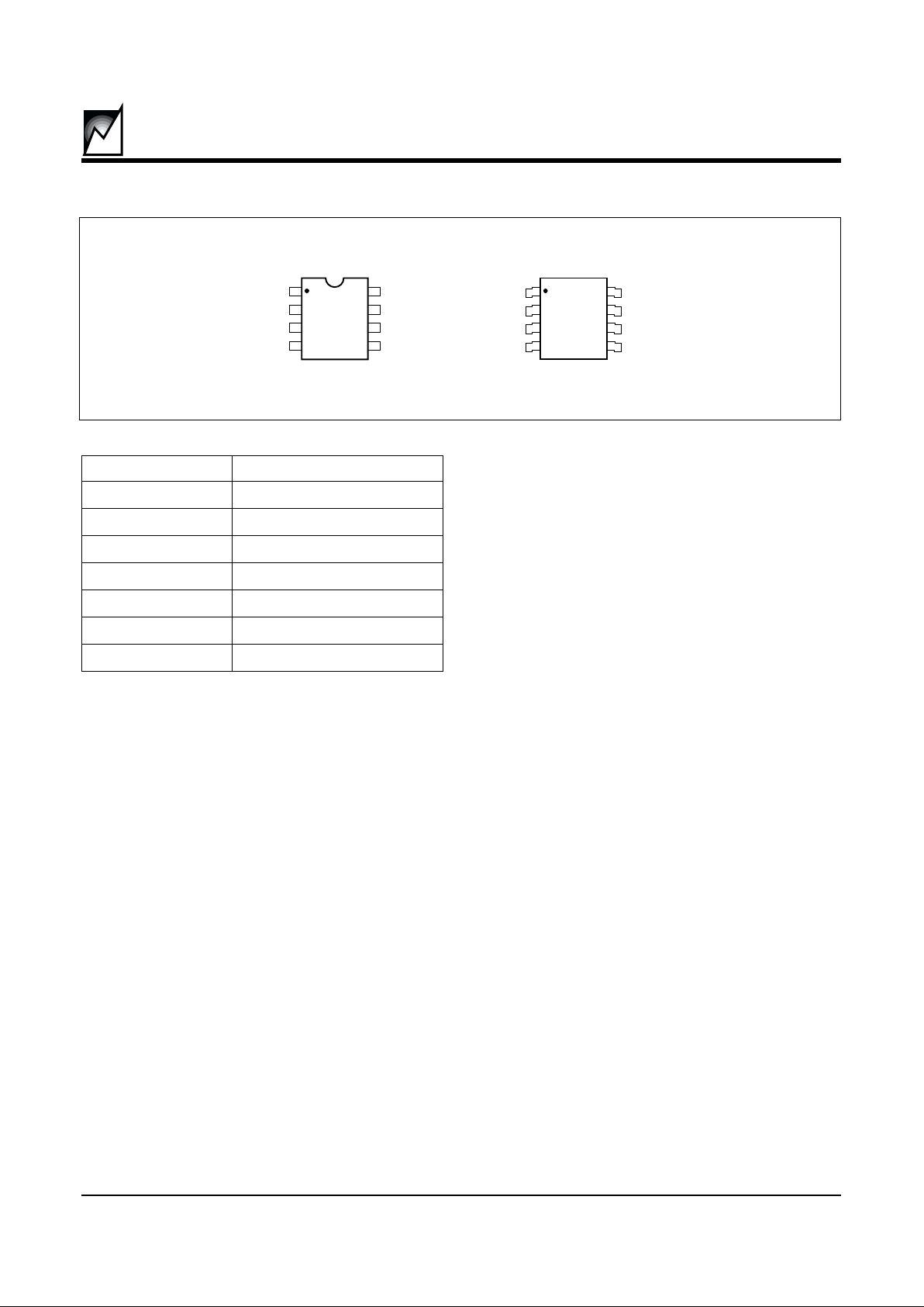
PIN FUNCTIONS
Pin Name Function
CS Chip Select
SK Clock Input
DI Serial Data Input
DO Serial Data Output
V
CC
+2.7 to 6.0V Power Supply
GND Ground
NC No Connect
PIN CONFIGURATION
DIP Package (P)
SOIC Package (S)
DEVICE OPERATION
WRITE LOCKOUT DESCRIPTION
The S93VP462/VP463 provides a precision internal
reset controller that ensures correct system operation
during brown-out and power-up/-down conditions.
During power-up, the write lockout remains active until
V
CC
reaches the V
TRIP
threshold. Write lockout will
continue to be driven for approximately 150 ms after V
CC
reaches V
TRIP
. During power-down, write lockout will be
driven active when even V
CC
falls below V
TRIP
.
GENERAL OPERATION
The S93VP462/VP463 is a 1024-bit nonvolatile memory
intended for use with industry standard microproces-
sors. The S93VP463 is organized as X16, seven 9-bit
instructions control the reading, writing and erase
operations of the device. The S93VP462 is organized as
X8, seven 10-bit instructions control the reading, writing
and erase operations of the device. The device operates
on a single 3V or 5V supply and will generate on chip, the
high voltage required during any write operation.
Instructions, addresses, and write data are clocked into
the DI pin on the rising edge of the clock (SK). The DO
pin is normally in a high impedance state except when
reading data from the device, or when checking the
ready/busy status after a write operation.
The ready/busy status can be determined after the start
of a write operation by selecting the device (CS high) and
polling the DO pin; DO low indicates that the write
operation is not completed, while DO high indicates that
the device is ready for the next instruction. See the
Applications Aid section for detailed use of the ready
busy status.
The format for all instructions is: one start bit; two op
code bits and either six (x16) or seven (x8) address or
instruction bits.
2040 ILL1.0
CS
SK
DI
DO
V
CC
NC
NC
GND
1
2
3
4
8
7
6
5
CS
SK
DI
DO
V
CC
NC
NC
GND
1
2
3
4
8
7
6
5
3
S93VP462/S93VP463
2040-01 10/23/98
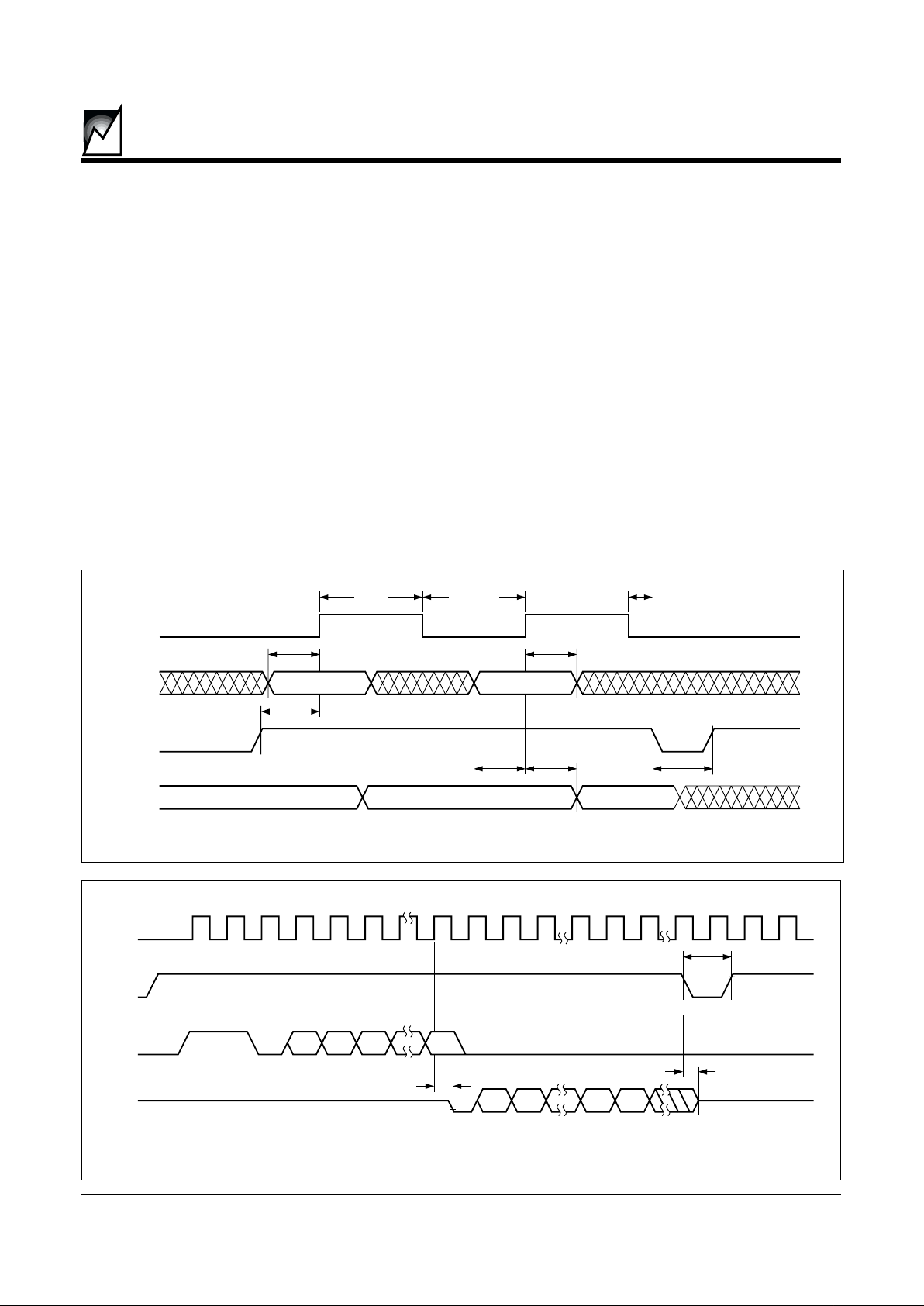
Read
Upon receiving a READ command and an address
(clocked into the DI pin), the DO pin of the S93VP462/
VP463 will come out of the high impedance state and,
will first output an initial dummy zero bit, then begin
shifting out the data addressed (MSB first). The output
data bits
will toggle on the rising edge of the SK clock and
are stable after the specified time delay
(t
PD0
or t
PD1
).
Write
After receiving a WRITE command, address and the
data, the CS (Chip Select) pin must be deselected for a
minimum of 250ns (t
CSMIN
). The falling edge of CS will
start automatic erase and write cycle to the memory
location specified in the instruction. The ready/busy
status of the S93VP462/VP463 can be determined by
selecting the device and polling the DO pin.
Erase
Upon receiving an ERASE command and address, the
CS (Chip Select) pin must be deselected for a minimum
of 250ns (t
CSMIN
). The falling edge of CS will start the
auto erase cycle of the selected memory location. The
ready/busy status of the S93VP462/VP463 can be
determined by selecting the device and polling the DO
pin. Once cleared, the content of a cleared location
returns to a logical “1” state.
Figure 1. Sychronous Data Timing
Figure 2. Read Instruction Timing
SK
2040 ILL 3.0
DI
CS
DO
t
DIS
t
PD0,
t
PD1
t
CSMIN
t
CSS
t
DIS
t
DIH
t
SKHI
t
CSH
VALID VALID
DATA VALID
t
SKLOW
SK
2040 ILL4.0
CS
DI
DO
t
CS
STANDBY
t
HZ
HIGH-ZHIGH-Z
11 0
A
N
A
N–1
A
0
0
D
N
D
N–1
D
1
D
0
t
PD0

4
S93VP462/S93VP463
2040-01 10/23/98
Erase/Write Enable and Disable
The S93VP462/VP463 powers up in the write disable
state. Any writing after power-up or after an EWDS
(write disable) instruction must first be preceded by the
EWEN (write enable) instruction.
Once the write in-
struction is enabled, it will remain enabled until power to
the device is removed, or the EWDS instruction is sent.
The EWDS instruction can be used to disable all
S93VP462/VP463 write and clear instructions, and will
prevent any accidental writing or clearing of the device.
Data can be read normally from the device regardless
of the write enable/disable status.
Erase All
Upon receiving an ERAL command, the CS (Chip
Select) pin must be deselected for a minimum of 250ns
(t
CSMIN
). The falling edge of CS will start the self clocking
clear cycle of all memory locations in the device. The
clocking of the SK pin is not necessary after the device
has entered the self clocking mode. The ready/busy
status of the S93VP462/VP463 can be determined by
selecting the device and polling the DO pin. Once
cleared, the contents of all memory bits will be in a
logical “1” state.
Write All
Upon receiving a WRAL command and data, the CS
(Chip Select) pin must be deselected for a minimum of
250ns (t
CSMIN
). The falling edge of CS will start the self
clocking data write to all memory locations in the device.
The clocking of the SK pin is not necessary after the
device has entered the self clocking mode. The ready/
busy status of the S93VP462/VP463 can be determined
by selecting the device and polling the DO pin. It is not
necessary for all memory locations to be cleared before
the WRAL command is executed.
Page Write
93462 - Assume WEN has been issued. The host will
then take CS high, and begin clocking in the start bit,
write command and 7-bit address immediately fol-
lowed by the first byte of data to be written. The host
can then continue clocking in 8-bit bytes of data with
each byte to be written to the next higher address.
Internally the address pointer is incremented after
receiving each group of eight clocks; however, once
the address counter reaches xxx 1111 it will roll over
to xxx 0000 with the next clock. After the last bit is
clocked in no internal write operation will occur until CS
is brought low.
93463 - Assume WEN has been issued. The host will
then take CS high, and begin clocking in the start bit,
write command and 6-bit address immediately
followed by the first 16-bit word of data to be written.
The host can then continue clocking in 16-bit words of
data with each word to be written to the next higher
address. Internally the address pointer is incremented
after receiving each group of sixteen clocks; however,
once the address counter reaches xxx x111 it will roll
over to xx x000 with the next clock. After the last bit is
clocked in no internal write operation will occur until CS
is brought low.
Continuous Read
This begins just like a standard read with the host
issuing a read instruction and clocking out the data
byte [word]. If the host then keeps CS high and
continues generating clocks on SK, the S93VP462/
VP463 will output data from the next higher address
location. The S93VP462/VP463 will continue
incrementing the address and outputting data so long
as CS stays high. If the highest address is reached, the
address counter will roll over to address 0000. CS
going low will reset the instruction register and any
subsequent read must be initiated in the normal man-
ner of issuing the command and address.
 Loading...