


SUMMIT SMP9212G, SMP9212S, SMP9210G, SMP9210S, SMP9211G Datasheet
...SUMMIT |
SMP9210, -11, -12 |
MICROELECTRONICS, Inc. |
Dual 10-Bit Nonvolatile DAC
Preliminary
FEATURES
!Two 10-Bit Nonvolatile DACs
"INL ±1LSB
"DNL ±1LSB
!Programmable Configuration
!Programmable Power On Reset Options
"Recall Full Scale Value
"Recall Zero Scale Value
"Recall Mid-Scale Value
"Recall NV Register Value
!Tandem or Independent Operation of DACs
!Programmable Power Down Mode (Short VOUT to GND or Float VOUT)
!I2C Interface
!Low Noise Outputs
!2.7V to 5.5V Operation
!–40ºC to 85ºC Temperature Range
APPLICATIONS
! ATE Set and Forget Calibration |
! RFPA Biasing |
! Laser Biasing |
|
|
|
SIMPLIFIED APPLICATION DRAWING |
|
|
|
I2C
IN+
IN–
GND
|
SMP9210 |
|
|
|
VOUT1 |
|
3.3V |
|
|
|
|
|
|
|
MONITOR |
|
|
|
DIODE |
|
|
|
LASER |
MODMON |
APCSET |
CC |
DIODE |
|
|||
V |
MD |
||
|
|
|
|
|
Laser Driver |
|
RDAMP |
MODSET |
BIASSET |
|
IMOD |
APC |
IBIAS |
||
|
|
|
|
VOUT1 |
VOUT2 |
|
RFILT |
|
CAPC |
||
|
|
|
1nF |
SMP9210 |
|
|
|
2048 SAD
©SUMMIT MICROELECTRONICS, Inc., 2001 • 300 Orchard City Dr., Suite 131 • Campbell, CA 95008 • Phone 408-378-6461 • FAX 408-378-6586 • www.summitmicro.com
Characteristics subject to change without notice |
2048 3.3 10/03/01 |
1 |
SMP9210, SMP9211, SMP9212
Preliminary
INTRODUCTION
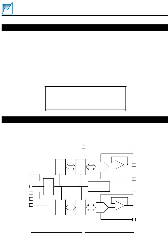
The SMP9210, -11, -12 trio are serial input, voltage output, dual 10-Bit digital to analog converters. They can operate from a single 2.7V to 5.5V supply. Internal precision buffers swing rail-to-rail with an input reference range from ground to the positive supply.
They integrate two 10-Bit DACs and their associated circuits: an enhanced unity gain operational amplifier
output, a 10-Bit volatile data latch, a 10-bit nonvolatile data register and an industry standard 2-wire serial interface.
Programming of configuration, control and calibration values by the user can be simplified with the interface adapter and Windows GUI software obtainable from Summit Microelectronics.
RECOMMENDED OPERATING CONDITIONS
Temperature |
–40ºC to 85ºC. |
Voltage |
2.7V to 5.5V |
FUNCTIONAL BLOCK DIAGRAMS
Note: Pinouts for these three drawings reflect the 14 pin SOIC package.
A0 3
A1 2 
A2 1
SDA 14
SCL 12
CS 8
|
|
|
VDD |
|
|
|
|
|
|
13 |
|
|
|
|
|
VOLATILE REGISTER |
VOLATILE CONTROL REGISTER |
|
4 |
VREFH2 |
|
NON- |
10-BIT |
6 |
VOUT2 |
||
|
|
|
|
|||
|
|
|
|
DAC |
|
|
INTERFACE CONTROL& |
LOGIC |
|
|
|
5 |
VREFL2 |
|
|
CONFIGURATION |
|
|
||
|
|
|
|
|
|
|
|
|
|
|
REGISTER |
|
|
|
|
VOLATILE REGISTER |
VOLATILE CONTROL REGISTER |
|
11 |
VREFH1 |
|
NON- |
10-BIT |
9 |
VOUT1 |
||
|
|
|
|
|||
|
|
|
|
DAC |
|
|
|
|
|
SMP9210 |
10 VREFL1 |
||
|
|
|
|
|
||
|
|
|
7 |
|
|
|
|
|
|
GND |
|
2048 BD10 2.2 |
|
2 |
2048 3.3 10/03/01 |
SUMMIT MICROELECTRONICS, Inc. |

SMP9210, SMP9211, SMP9212
Preliminary
|
|
|
|
|
VDD |
|
|
|
|
|
|
|
|
13 |
|
|
|
|
|
|
|
VOLATILE REGISTER |
VOLATILE CONTROL REGISTER |
|
4 |
VREFH2 |
|
|
|
NON- |
10-BIT |
6 |
VOUT2 |
||
|
|
|
|
|
|
|||
|
|
|
|
|
|
DAC |
|
|
A0 |
3 |
|
|
|
|
|
|
|
A1 |
2 |
INTERFACE CONTROL& |
|
|
|
|
5 |
VREFL2 |
A2 |
1 |
LOGIC |
|
|
CONFIGURATION |
|
|
|
|
|
|
|
|
|
|||
|
|
|
|
REGISTER |
|
|
||
|
|
|
|
|
|
|
|
|
SDA |
14 |
|
|
|
|
|
11 |
VREFH1 |
|
|
|
|
|
|
|
||
SCL |
12 |
|
|
VOLATILE REGISTER |
VOLATILE CONTROL REGISTER |
|
|
|
|
|
|
NON- |
10-BIT |
9 |
VOUT1 |
||
|
|
|
|
|
|
|||
|
|
|
|
|
|
DAC |
|
|
|
|
|
|
|
|
|
8 |
MUTE# |
|
|
|
|
|
|
|
10 VREFL1 |
|
|
|
|
|
|
SMP9211 |
|
|
|
|
|
|
|
|
7 |
|
|
|
|
|
|
|
|
GND |
|
2048 BD11 2.2 |
|
|
|
|
|
|
VDD |
|
|
|
|
|
|
|
|
13 |
|
|
|
|
|
|
|
VOLATILE REGISTER |
VOLATILE CONTROL REGISTER |
|
4 |
VREFH2 |
|
|
|
NON- |
10-BIT |
6 |
VOUT2 |
||
|
|
|
|
|
|
|||
|
|
|
|
|
|
DAC |
|
|
A0 |
3 |
|
|
|
|
|
|
|
A1 |
2 |
INTERFACE CONTROL& |
|
|
|
|
5 |
VREFL2 |
A2 |
1 |
LOGIC |
|
|
CONFIGURATION |
|
|
|
|
|
|
|
REGISTER |
|
|
||
|
|
|
|
|
|
|
|
|
SDA |
14 |
|
|
|
|
|
11 |
VREFH1 |
|
|
|
|
|
|
|
||
SCL |
12 |
|
|
VOLATILE REGISTER |
VOLATILE CONTROL REGISTER |
|
|
|
|
|
|
NON- |
10-BIT |
9 |
VOUT1 |
||
|
|
|
|
|
|
|||
|
|
|
|
|
|
DAC |
|
|
VREF |
8 |
PRECISION |
|
|
|
10 VREFL1 |
||
|
SMP9212 |
|
|
|||||
|
|
REFERENCE |
|
|
|
|||
|
|
|
|
|
7 |
|
|
|
|
|
|
|
|
GND |
|
2048 BD12 3.0 |
|
SUMMIT MICROELECTRONICS, Inc. |
2048 3.3 10/03/01 |
3 |

SMP9210, SMP9211, SMP9212
|
|
|
|
|
|
|
|
|
|
|
|
|
|
|
|
|
|
|
|
|
|
|
|
|
|
|
|
|
|
|
|
|
|
|
Preliminary |
|
|
|
|
|
|
|
|
|
|
|
|
|
|
|
|
|
|
|
|
|
|
|
|
|
|
|
|
|
|
|
|
|
|
|
|
PIN CONFIGURATIONS |
|
|
|
|
|
|
|
|
|
|
|
|
|
|
|
|
|
|
|
|
|
|
|
|
|
||||||||||
|
|
|
|
|
|
|
|
|
|
|
|
|
|
|
|
|
|
|
|
|
|
|
|
|
|
|
|
|
|
|
|
|
|
|
|
|
|
|
|
|
|
|
|
|
|
|
|
|
|
14-Pin SOIC |
|
|
|
|
|
|
|
|
|
|
|
|
|
|
|
|
|
|
|||
|
|
|
|
|
|
|
SMP9210 |
|
|
|
|
SMP9211 |
|
|
|
|
|
|
|
|
|
|
|
|
|
SMP9212 |
|
|
|
||||||
|
|
|
|
|
|
|
|
|
|
|
|
|
|
|
|
|
|
|
|
|
|
|
|
|
|
|
|
|
|
|
|
|
|
|
|
A2 |
|
|
|
1 |
14 |
|
SDA |
A2 |
|
1 |
14 |
|
|
SDA |
A2 |
|
|
|
|
1 |
14 |
|
|
SDA |
|||||||||||
A1 |
|
|
|
|
|
2 |
13 |
|
VDD |
A1 |
|
|
2 |
13 |
|
|
VDD |
A1 |
|
|
|
|
|
2 |
13 |
|
|
VDD |
|||||||
A0 |
|
|
|
|
3 |
12 |
|
SCL |
A0 |
|
3 |
12 |
|
|
SCL |
A0 |
|
|
|
|
3 |
12 |
|
|
SCL |
||||||||||
|
|
|
|
|
|
|
|
|
|
|
|
|
|||||||||||||||||||||||
VREFH2 |
|
|
|
|
4 |
11 |
|
VREFH1 |
VREFH2 |
|
4 |
11 |
|
|
VREFH1 |
VREFH2 |
|
|
|
|
4 |
11 |
|
|
VREFH1 |
||||||||||
|
|
|
|
|
|
|
|
|
|
|
|
|
|||||||||||||||||||||||
VREFL2 |
|
|
5 |
10 |
|
VREFL1 |
VREFL2 |
|
5 |
10 |
|
|
VREFL1 |
VREFL2 |
|
|
5 |
10 |
|
|
VREFL1 |
||||||||||||||
|
|
|
|
|
|
|
|
|
|||||||||||||||||||||||||||
VOUT2 |
|
|
6 |
9 |
|
VOUT1 |
VOUT2 |
|
6 |
9 |
|
|
VOUT1 |
VOUT2 |
|
|
|
6 |
9 |
|
|
VOUT1 |
|||||||||||||
|
|
|
|
|
|
|
|
|
|
||||||||||||||||||||||||||
GND |
|
|
7 |
8 |
|
CS |
GND |
|
7 |
8 |
|
|
MUTE# |
GND |
|
|
|
7 |
8 |
|
|
VREF |
|||||||||||||
|
|
|
|
|
|
|
|
||||||||||||||||||||||||||||
|
|
|
|
|
|
|
|
|
|
|
|
|
|
|
|
|
|
|
|
|
|
|
|
|
|
|
|
|
|
|
|
|
2048 14-PCon |
||
|
|
|
|
|
|
|
|
|
|
|
|
|
|
16-Pin SSOP |
|
|
|
|
|
|
|
|
|
|
|
|
|
|
|
|
|
|
|||
|
|
|
|
|
|
|
SMP9210 |
|
|
|
|
SMP9211 |
|
|
|
|
|
|
|
|
|
|
|
|
|
SMP9212 |
|
|
|
||||||
A2 |
|
|
|
|
|
|
|
|
|
|
|
|
|
|
|
|
|
|
|
|
|
|
|
|
|
|
|
||||||||
|
|
1 |
16 |
|
SDA |
A2 |
|
1 |
16 |
|
|
SDA |
A2 |
|
|
|
1 |
16 |
|
SDA |
|||||||||||||||
|
|
|
|
|
|
|
|
|
|
|
|
|
|||||||||||||||||||||||
|
|
|
|
|
|
|
|
|
|
|
|
|
|||||||||||||||||||||||
NC |
|
|
2 |
15 |
|
NC |
NC |
|
2 |
15 |
|
|
NC |
NC |
|
|
|
|
2 |
15 |
|
NC |
|||||||||||||
|
|
|
|
|
|
|
|
|
|
|
|
|
|
||||||||||||||||||||||
A1 |
|
|
3 |
14 |
|
VDD |
A1 |
|
3 |
14 |
|
|
VDD |
A1 |
|
|
|
3 |
14 |
|
VDD |
||||||||||||||
|
|
|
|
|
|
|
|
|
|
|
|
|
|||||||||||||||||||||||
A0 |
|
|
4 |
13 |
|
SCL |
A0 |
|
4 |
13 |
|
|
SCL |
A0 |
|
|
|
|
4 |
13 |
|
SCL |
|||||||||||||
VREFH2 |
|
|
5 |
12 |
|
VREFH1 |
VREFH2 |
|
5 |
12 |
|
|
VREFH1 |
VREFH2 |
|
|
|
|
5 |
12 |
|
VREFH1 |
|||||||||||||
|
|
|
|
|
|
|
|
|
|
|
|
|
|
||||||||||||||||||||||
|
|
|
|
|
|
|
|
|
|
|
|
|
|
||||||||||||||||||||||
VREFL2 |
|
|
|
6 |
11 |
|
VREFL1 |
VREFL2 |
|
6 |
11 |
|
|
VREFL1 |
VREFL2 |
|
|
|
|
|
|
|
6 |
11 |
|
VREFL1 |
|||||||||
|
|
|
|
|
|
|
|
|
|
|
|
|
|
|
|
|
|||||||||||||||||||
VOUT2 |
|
|
7 |
10 |
|
VOUT1 |
VOUT2 |
|
7 |
10 |
|
|
VOUT1 |
VOUT2 |
|
|
|
|
7 |
10 |
|
VOUT1 |
|||||||||||||
|
|
|
|
|
|
|
|
|
|
|
|
|
|
||||||||||||||||||||||
GND |
|
|
|
8 |
9 |
|
CS |
GND |
|
8 |
9 |
|
|
MUTE# |
GND |
|
|
|
|
|
|
8 |
9 |
|
VREF |
||||||||||
|
|
|
|
|
|
|
|
|
|
|
|
|
|
|
|
||||||||||||||||||||
2048 16-PCon
PIN DESCRIPTIONS
VDD
Power supply input.
GND
Power supply return.
VOUT1, VOUT2
The voltage output of the DACs. It is buffered by a unitygain follower that can slew up to 1V/µs.
VREFL1, VREFL2
The lower of the voltage reference inputs. VREFL must be equal to or greater than ground and less than VREFH.
VREFH1, VREFH2
The higher of the voltage reference inputs. VREFHmustbe equal to or less than VCC and greater than VREFL.
A0, A1, A2
The address inputs for the serial interface logic. Biasing the address inputs will determine the device’s bus address that is contained within the serial data stream when communicating over the serial bus.
SCL
The serial interface clock. It is used to clock the data in and out. When writing to the device data must remain stable while SCL is high. When reading from the device data is clocked out on the falling edge of SCL.
SDA
The bidirectional pin used to transfer data in and out of the device.
CS
Chip Select input (VIH = selected) in the 9210. See the Block Diagrams.
MUTE#
Mute input (VIL = mute) in the 9211. See the Block Diagrams.
VREF
VREF output (1.25V) in the 9212. See the Block Diagrams.
Note: NC pins are not connected.
4 |
2048 3.3 10/03/01 |
SUMMIT MICROELECTRONICS, Inc. |
 Loading...