


SUMMIT S24163PA, S24163PAT, S24163PB, S24163PBT, S24163S2.7 Datasheet
...SUMMIT
|
MICROELECTRONICS, Inc. |
|
S24163 |
|
Precision RESET Controller with 16K I2C Memory |
3 and 5 Volt Systems |
|
||
FEATURES |
|
|
|
|
• |
Precision Supply Voltage Monitor |
• High Reliability |
|
|
|
— Active Low |
— Endurance: 100,000 erase/write cycles |
||
|
— Integrated memory write lockout |
— Data retention: 100 years |
||
• |
Guaranteed RESET (RESET#) assertion |
• 8-Pin PDIP or SOIC Packages |
||
|
to VCC = 1V |
|
|
|
•Power-Fail Accuracy Guaranteed
•No External Components
•3V and 5V system versions
•Low Power CMOS
—Active current less than 3mA
—Standby current less than 25µA
•Memory Internally Organized 2k X 8
—Two Wire Serial Interface (I2C™)
–Bidirectional data transfer protocol
–Standard 100KHz and Fast 400KHz
OVERVIEW
The S24163 is a power supervisory device with 16,384bits of serial E2PROM. It is fabricated using SUMMIT's advanced CMOS E2PROM technology and is suitable for both 3 and 5 volt systems.
The S24163 is internally organized as 2048 x 8. It features the I2C serial interface and software protocol allowing operation on a simple two-wire bus.
BLOCK DIAGRAM
VCC 8
SCL |
|
|
|
|
|
|
|
|
|
||
|
|
|
|
||
|
|
|
|
||
6 |
|
|
|
||
|
|
|
|
|
|
SDA |
|
5 |
|
|
|
|
5kHz |
RESET |
2 |
RESET# |
|
PULSE |
|
|
|
OSCILLATOR |
|
|
||
|
|
|
||
|
GENERATOR |
|
|
|
+ |
VTRIP |
RESET |
|
|
– |
CONTROL |
|
|
|
1.26V |
|
|
|
|
MODE |
ADDRESS |
WRITE |
|
|
DECODE |
DECODER |
CONTROL |
|
|
DATA I/O |
E2PROM |
|
|
|
MEMORY |
|
|
||
|
|
ARRAY |
|
|
4
GND |
2014 T BD 2.0 |
|
|
|
|
SUMMIT MICROELECTRONICS, Inc. • 300 Orchard City Drive, Suite 131 |
• Campbell, CA 95008 • Telephone 408-378-6461 • Fax 408-378-6586 • www.summitmicro.com |
|
|
© SUMMIT MICROELECTRONICS, Inc. 2000 |
Characteristics subject to change without notice |
20142.0 3/21/00 |
1 |

S24163
PIN CONFIGURATION
SMS24163 8-Pin PDIP or 8-Pin SOIC
NC |
|
|
1 |
8 |
|
VCC |
|
|
|
|
|||||
|
|
|
|||||
RESET# |
|
|
|
2 |
7 |
|
NC |
|
|
|
|
||||
|
|
|
|
||||
NC |
|
|
3 |
6 |
|
SCL |
|
|
|
|
|||||
|
|
|
|||||
VSS |
|
|
4 |
5 |
|
SDA |
|
|
|
|
|||||
|
|
|
|||||
2014 T PCon 2.0
PIN DESCRIPTIONS
SCL — Serial Clock: The SCL input is used to clock data into and out of the device. In the WRITE mode data must remain stable while SCL is HIGH. In the READ mode data is clocked out on the falling edge of SCL.
SDA — Serial Data: The SDA pin is a bidirectional pin used to transfer data into and out of the device. Data may change only when SCL is LOW, except START and STOP conditions. It is an open-drain output and may be wireORed with any number of open-drain or open-collector outputs.
RESET# — Reset: This is an active low open drain output. It is driven low whenever VCC is below VTRIP. It is also an input and can be used to debounce a switch input or perform signal conditioning. The pin has an internal pull-up and should be left unconnected if the signal is not used in the system. However, an external pull-up resistor must be connected when the pin is tied to a system RESET# line.
VCC — Power: VCC is the voltage input, typically 2.7 to 5.5 volts.
GND — Ground: Power return.
NC — No Connect: The no connect inputs are not used. However, to ensure proper operation, they can be unconnected or tied to ground. They must not be tied to VCC.
ENDURANCE AND DATA RETENTION
The S24163 is designed for applications requiring up to 100,000 erase/write cycles and unlimited read cycles. It provides 100 years of secure data retention, with or without power applied, after the execution of 100,000 erase/write cycles.
APPLICATIONS
The S24163 is ideal for applications requiring low voltage and low power consumption. This device provides microcontroller RESET control and can be manually
resettable. This device also uses a cost effective, spacesaving, 8-pin SOIC or PDIP plastic package. Typical
applications include alarm devices, electronic locks, meters, keys, pagers and cellular phones.
RESET CONTROLLER DESCRIPTION
The device provides a precise reset output to a microcontroller and it’s associated circuitry ensuring correct system operation during power-up/down conditions and brownout situations. The output is open drain, allowing control of the reset function by multiple devices.
During power-up the reset output remains in a fixed active state until VCC passes through the reset threshold and remains above the threshold for 200ms. The reset output is valid whenever VCC ≥ 1V. If VCC falls below the threshold for more than tGLITCH the device will immediately generate a reset and drive the output.
The reset pin is an I/O; therefore, forcing the pin to the active state can also manually reset the device. Because the I/O needs to be an open drain, the internal timer can only be triggered by the leading edge of the input. The resulting reset output will either be tPURST, or the externally applied reset signal, whichever is longer. This can provide an affective debounce or reset signal extender solution.
CHARACTERISTICS OF THE I2C BUS
General Description
The I2C bus was designed for two-way, two-line serial communication between different integrated circuits. The two lines are a serial data line (SDA), and a serial clock line (SCL). The SDA line must be connected to a positive supply by a pull-up resistor, located somewhere on the bus (See Figure 1). Data transfer between devices may be initiated with a START condition only when SCL and SDA are HIGH (bus is not busy).
2014 2.0 3/21/00
2

|
|
|
|
S24163 |
|
|
|
|
VCC |
|
|
SDA |
|
|
|
|
|
|
|
|
RESET |
|
|
SCL |
|
|
|
|
|
Master |
Slave |
Slave |
Master |
Master |
|
Transmitter/ |
Transmitter/ |
Transmitter/ |
|||
Receiver |
Transmitter |
||||
Receiver |
Receiver |
Receiver |
|||
|
|
||||
|
|
(24163) |
|
(µC/ µP) |
|
|
|
|
|
2014 T fig01 2.0 |
|
|
FIGURE 1. TYPICAL SYSTEM CONFIGURATION |
|
|||
SCL |
Data must |
|
|
|
Data must |
|
remain stable |
Change |
remain stable |
||
|
while clock |
of data |
|
while clock |
|
|
is HIGH. |
allowed |
|
is HIGH. |
|
SDA In |
|
|
|
|
|
|
tHD:DAT |
tSU:DAT |
tHD:DAT |
||
|
|
|
|
|
2014 ILL4 1.0 |
|
FIGURE 2. INPUT DATA PROTOCOL |
||||
SCL |
|
START |
STOP |
Condition |
Condition |
SDA In |
|
|
2014 ILL5 1.0 |
|
FIGURE 3. START AND STOP CONDITIONS |
|
2014 2.0 3/21/00 |
|
3 |
|
|
|
S24163 |
|
SCL from |
1 |
8 |
9 |
|
Master |
||||
|
|
|
||
|
Start |
|
|
|
Data Output |
Condition |
|
|
|
|
|
|
||
from |
|
|
tAA |
|
Transmitter |
|
|
||
|
|
|
||
Data Output |
|
|
|
|
from |
|
tAA |
ACKnowledge |
|
Receiver |
|
|||
|
|
|||
|
FIGURE 4. ACKNOWLEDGE RESPONSE FROM RECEIVER |
2014 ILL6 1.0 |
||
|
|
|||
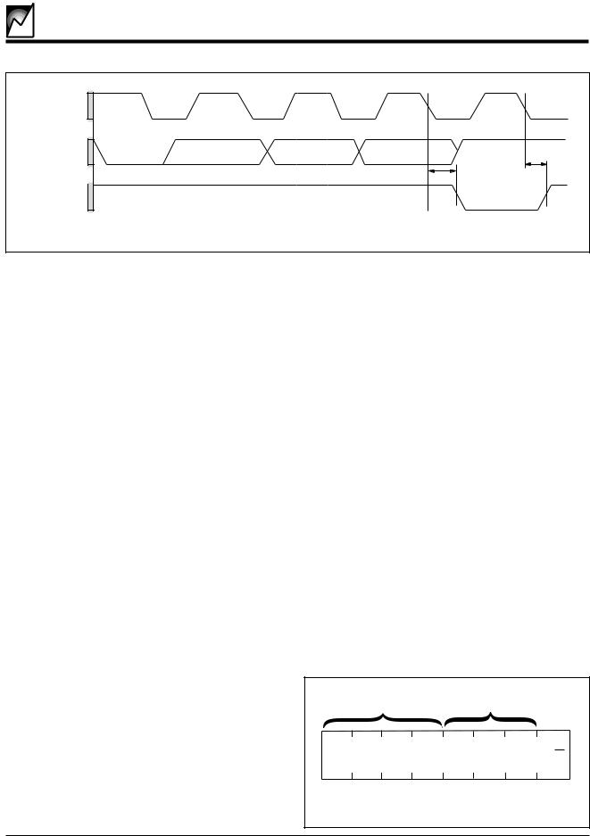
Input Data Protocol
One data bit is transferred during each clock pulse. The data on the SDA line must remain stable during clock HIGH time, because changes on the data line while SCL is HIGH will be interpreted as start or stop condition (See Figure 2).
START and STOP Conditions
When both the data and clock lines are HIGH, the bus is said to be not busy. A HIGH-to-LOW transition on the data line, while the clock is HIGH, is defined as the “START” condition. A LOW-to-HIGH transition on the data line, while the clock is HIGH, is defined as the “STOP” condition (See Figure 3).
DEVICE OPERATION
The S24163 is a 16,384-bit serial E2PROM. The device supports the I2C bidirectional data transmission protocol. The protocol defines any device that sends data onto the bus as a “transmitter” and any device which receives data as a “receiver.” The device controlling data transmission is called the “master” and the controlled device is called the “slave.” Since it never initiates any data transfers the S24163 is always a “slave” device.
Acknowledge (ACK)
Acknowledge is a software convention used to indicate successful data transfers. The transmitting device, either the master or the slave, will release the bus after transmitting eight bits. During the ninth clock cycle, the receiver will pull the SDA line LOW to ACKnowledge that it received the eight bits of data (See Figure 4).
The S24163 will respond with an ACKnowledge after recognition of a START condition and its slave address byte. If both the device and a write operation are selected, the S24163 will respond with an ACKnowledge after the receipt of each subsequent 8-bit word.
In the READ mode the S24163 transmits eight bits of data, then releases the SDA line, and monitors the line for an ACKnowledge signal. If an ACKnowledge is detected, and no STOP condition is generated by the master, the S24163willcontinuetotransmitdata.IfanACKnowledgeis notdetectedtheS24163willterminatefurtherdatatransmissions and await a STOP condition before returning to the standby power mode.
Device Addressing
Following a start condition the master must output the address of the slave it is accessing. The most significant four bits of the slave address are the device type identifier (see figure 5). For the S24163 this is fixed as 1010[BHEX].
Word Address
The next three bits of the slave address are an extension of the array’s address and are concatenated with the eight bits of address in the word address field, providing direct access to the 2,048 X 8 array.
Read/Write Bit
The last bit of the data stream defines the operation to be performed. When set to “1” a read operation is selected; when set to “0” a write operation is selected.
DEVICE |
HIGH ORDER |
IDENTIFIER |
WORD ADDRESS |
1 |
0 |
1 |
0 |
A10 |
A9 |
A8 |
R/W |
|
|
|
|
|
|
2014 ILL7 1.0 |
|
FIGURE 5. SLAVE ADDRESS BYTE
2014 2.0 3/21/00
4
 Loading...