


SUMMIT S24022PAT, S24022PB, S24022PBT, S24023P2.7, S24023P2.7T Datasheet
...SUMMIT
MICROELECTRONICS, Inc. |
S24042/S24043 |
Precision RESET Controller and 4K I2C Memory |
3 and 5 Volt Systems |
With Both RESET and RESET Outputs |
|
FEATURES
•Precision Supply Voltage Monitor
—Dual reset outputs for complex microcontroller systems
—Integrated memory write lockout
•Guaranteed RESET (RESET#) assertion to VCC=1V
•Power-Fail Accuracy Guaranteed
•No External Components
•3 and 5 Volt system versions
•Low Power CMOS
—Active current less than 3mA
—Standby current less than 25µA
•Memory Internally Organized 512 X 8
—Two Wire Serial Interface (I2C™)
–Bidirectional data transfer protocol
–Standard 100KHz and Fast 400KHz
•High Reliability
—Endurance: 100,000 erase/write cycles
—Data retention: 100 years
•8-Pin PDIP or SOIC Packages
OVERVIEW
The S24042 and S24043 are power supervisory devices with 4,096 bits of serial E2PROM. They are fabricated using SUMMIT’s advanced CMOS E2PROM technology and are suitable for both 3 and 5 volt systems.
The memory is internally organized as 512 x 8. It features the I2C serial interface and software protocol allowing operation on a simple two-wire bus.
The S24042 provides a precision VCC sense circuit and two open drain outputs: one (RESET) drives high and the other (RESET#) drives low whenever VCC falls below
VTRIP. The S24043 is identical to the S24042 with the exception being RESET is not bonded out on pin 7.
BLOCK DIAGRAM
|
VCC |
|
|
|
|
|
|
|
|
|
|
|
22 |
|
|
|
|
|
|
|
|
|
|
|
|
|
|
5kHz |
|
RESET |
|
|
|
2 |
RESET# |
|
|
|
|
|
PULSE |
|
|
|
|||
|
|
|
OSCILLATOR |
|
|
|
|
||||
|
|
|
|
GENERATOR |
|
|
|
||||
|
|
|
|
|
|
|
|
|
|||
|
|
|
+ |
VTRIP |
RESET |
|
|
|
|
|
|
|
|
|
– |
|
|
CONTROL |
|
|
|
|
|
|
|
|
|
|
|
|
|
|
|
7 |
RESET |
|
|
|
1.26V |
|
|
|
|
|
|
|
|
SCL |
6 |
|
MODE |
|
ADDRESS |
|
WRITE |
|
|
|
|
|
|
|
|
|
|
|
|
||||
SDA |
5 |
|
DECODE |
|
DECODER |
CONTROL |
|
|
|
||
|
|
|
|
|
|
|
|
|
|
||
|
|
|
DATA I/O |
|
|
E2PROM |
|
|
|
|
|
|
|
|
|
|
MEMORY |
|
|
|
|
||
|
|
|
|
|
|
ARRAY |
|
|
|
|
|
|
4 |
|
|
|
|
|
|
|
|
|
|
|
GND |
|
|
|
|
|
2011 T-BD 1.0 |
|
|
||
|
|
|
|
|
|
|
|
|
|
||
SUMMIT MICROELECTRONICS, Inc. |
• |
300 Orchard City Drive, Suite 131 • |
Campbell, CA 95008 |
• |
Telephone 408-378- 6461 |
• |
Fax 408-378-6586 |
• www.summitmicro.com |
|||
© SUMMIT MICROELECTRONICS, Inc. 2000 |
Characteristics subject to change without notice |
2011 2.0 5/2/00 |
1 |

S24042/S24043
PIN CONFIGURATIONS
NC |
|
|
|
VCC |
1 |
|
8 |
||
RESET# |
|
S24042 |
|
RESET |
2 |
|
7 |
||
|
|
|
|
|
NC |
3 |
|
6 |
SCL |
VSS |
|
|
|
|
4 |
|
5 |
SDA |
|
|
|
|
|
|
NC |
|
|
|
VCC |
1 |
S24043 |
8 |
||
|
|
|
NC |
|
RESET# |
2 |
|
7 |
|
NC |
|
|
|
SCL |
3 |
|
6 |
||
|
|
|
|
SDA |
VSS |
4 |
|
5 |
|
|
|
|
|
|
|
|
2011 PCon 2.0 |
|
|
|
|
|
|
PIN NAMES |
||
|
|
|
|
|
SDA |
Serial Data I/O |
|
|
SCL |
Serial Clock Input |
|
|
RESET & RESET# |
Reset Output |
|
|
VSS |
Ground |
|
|
VCC |
Supply Voltage |
|
|
NC |
No Connect |
|
|
|
|
|
PIN DESCRIPTIONS
Serial Clock (SCL) - The SCL input is used to clock data into and out of the device. In the WRITE mode, data must remain stable while SCL is HIGH. In the READ mode, data is clocked out on the falling edge of SCL.
Serial Data (SDA) - The SDA pin is a bidirectional pin used to transfer data into and out of the device. Data may change only when SCL is LOW, except START and STOP conditions. It is an open-drain output and may be wireORed with any number of open-drain or open-collector outputs.
No Connects (NC) the no connect pins may be left floating or tied to ground. They cannot be tied high.
RESET #- RESET# is an active low open drain output. It is driven low whenever VCC is below VTRIP. It is also an input and can be used to debounce a switch input or perform signal conditioning. The pin has an internal pullup and should be left unconnected if the signal is not used in the system. However, when the pin is tied to a system RESET# line an external pull-up resistor should be employed.
RESET - RESET is an active high open drain output. It is driven high whenever VCC is below VTRIP. RESET is also an input and can be used to debounce a switch input or perform signal conditioning. The RESET pin does have an internal pull-down and should be left unconnected if the signal is not used in the system. However, when the pin is tied to a system reset line an external pull-down resistor should be employed.
ENDURANCE AND DATA RETENTION
The S24042/43 is designed for applications requiring 100,000 erase/write cycles and unlimited read cycles. It provides 100 years of secure data retention, with or without power applied, after the execution of 100,000 erase/write cycles.
APPLICATIONS
Reset Controller Description
The S24042/43 provides a precision RESET controller that ensures correct system operation during brown-out and power-up/-down conditions. It is configured with two open drain RESET outputs; pin 7 is an active high output and pin 2 is an active low output.
During power-up, the RESET outputs remain active until VCC reaches the VTRIP threshold and will continue driving the outputs for approximately 200ms after reaching VTRIP. The RESET outputs will be valid so long as VCC is > 1.0V. During power-down, the RESET outputs will begin driving active when VCC falls below VTRIP.
The RESET pins are I/Os; therefore, the S24042/43 can act as a signal conditioning circuit for an externally applied reset. The inputs are edge triggered; that is, the RESET input will initiate a reset timeout after detecting a low to high transition and the RESET# input will initiate a reset timeout after detecting a high to low transition. Refer to the applications Information section for more details on device operation as a reset conditioning circuit.
2011 2.0 5/2/00 |
SUMMIT MICROELECTRONICS, Inc. |
2
S24042/S24043
VCC = 3.0 0r 5.0
S24042 |
|
|
|
1 |
Vcc |
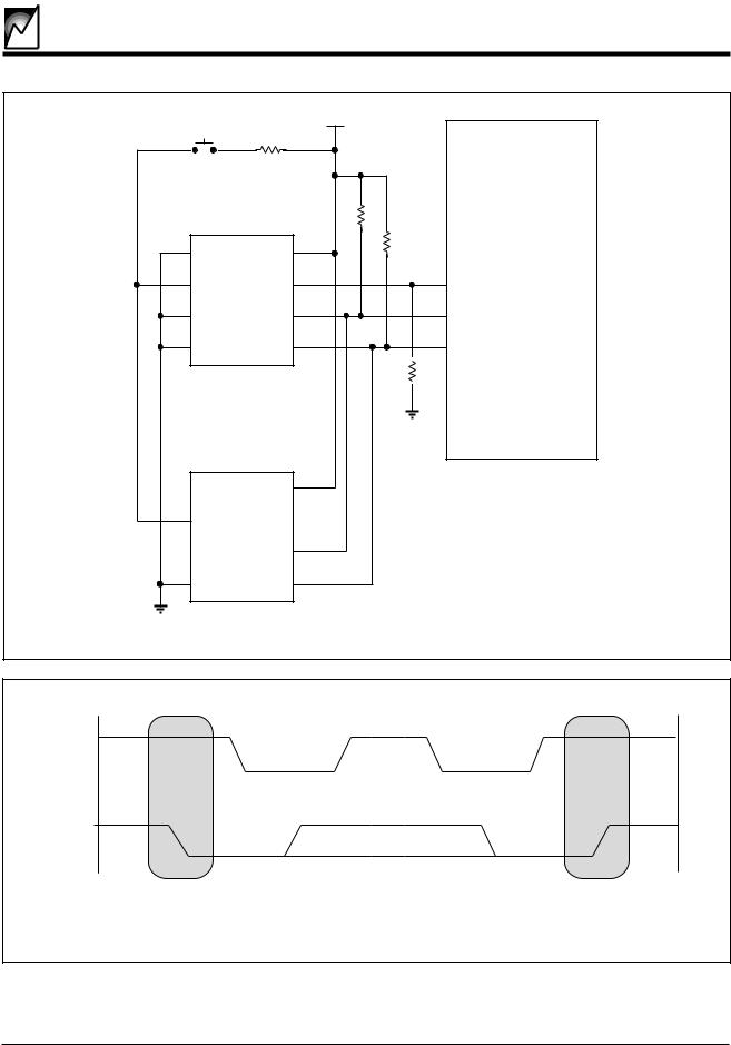
8 |
8051 Type MCU |
|
|
||
|
|
|
|
2 |
|
7 |
RESET |
RESET# |
RESET |
|
|
3 |
SCL |
6 |
|
|
|
SCL |
|
4 |
|
5 |
|
Vss |
SDA |
|
SDA |
I2C
Peripheral
RESET#
SCL |
|
SDA |
2011 T fig01 2.0 |
|
FIGURE 1. TYPICAL SYSTEM CONFIGURATION FOR DUAL RESET
SCL |
|
START |
STOP |
Condition |
Condition |
SDA In |
|
|
2011 ILL5 1.0 |
|
FIGURE 2. START AND STOP CONDITIONS |
2011 2.0 5/2/00 |
SUMMIT MICROELECTRONICS, Inc. |
3

|
|
|
S24042/S24043 |
|
SCL from |
1 |
8 |
9 |
|
Master |
||||
|
|
|
||
|
Start |
|
|
|
Data Output |
Condition |
|
|
|
|
|
|
||
from |
|
|
tAA |
|
Transmitter |
|
|
||
|
|
|
||
Data Output |
|
|
|
|
from |
|
|
ACKnowledge |
|
Receiver |
|
|
||
|
|
tAA |
||
|
|
|
2011 ILL6 1.0 |
|
|
FIGURE 3. ACKNOWLEDGE RESPONSE FROM RECEIVER |
|||
CHARACTERISTICS OF THE I2C BUS
General Description
The I2C bus was designed for two-way, two-line serial communication between different integrated circuits. The two lines are: a serial data line (SDA), and a serial clock line (SCL). The SDA line must be connected to a positive supply by a pull-up resistor, located somewhere on the bus (See Figure 1). Data transfer between devices may be initiated with a START condition only when SCL and SDA are HIGH (bus is not busy).
Input Data Protocol
One data bit is transferred during each clock pulse. The data on the SDA line must remain stable during clock HIGH time, because changes on the data line while SCL is HIGH will be interpreted as start or stop condition, refer to Figure 10.
START and STOP Conditions
When both the data and clock lines are HIGH, the bus is said to be not busy. A HIGH-to-LOW transition on the data line, while the clock is HIGH, is defined as the “START” condition. A LOW-to-HIGH transition on the data line, while the clock is HIGH, is defined as the “STOP” condition (See Figure 2).
DEVICE OPERATION
The S24042/43 is a 4,096-bit serial E2PROM. The device supports the I2C bidirectional data transmission protocol. The protocol defines any device that sends data onto the bus as a “transmitter” and any device which receives data as a “receiver.” The device controlling data transmission is called the “master” and the controlled device is called the “slave.” In all cases, the S24042/43 will be a “slave” device, since it never initiates any data transfers.
Acknowledge (ACK)
Acknowledge is a software convention used to indicate successful data transfers. The transmitting device, either the master or the slave, will release the bus after transmitting eight bits. During the ninth clock cycle, the receiver will pull the SDA line LOW to ACKnowledge that it received the eight bits of data (See Figure 3).
The S24042/43 will respond with an ACKnowledge after recognition of a START condition and its slave address byte. If both the device and a write operation are selected, the S24042/43 will respond with an ACKnowledge after the receipt of each subsequent 8-bit word.
In the READ mode, the S24042/43 transmits eight bits of data, then releases the SDA line, and monitors the line for an ACKnowledge signal. If an ACKnowledge is detected, and no STOP condition is generated by the master, the S24042/43 will continue to transmit data. If an ACKnowledge is not detected, the S24042/43 will terminate further data transmissions and awaits a STOP condition before returning to the standby power mode.
Device Addressing
Following a start condition the master must output the address of the slave it is accessing. The most significant four bits of the slave address are the device type identifier (see figure 4). For the S24042/43 this is fixed as 1010[B].
The next two bits are don’t care. The next bit is the high order address bit A8.
DEVICE |
|
IDENTIFIER |
DON’T CARE |
|
|
|
|
|
|
A |
|
|
|
|
1 |
0 |
1 |
0 |
X |
X |
R/W |
||||
8 |
||||||||||
|
|
|
|
|
|
|
|
|
||
|
|
|
|
|
|
2011 ILL7 1.1 |
||||
FIGURE 4. SLAVE ADDRESS BYTE
2011 2.0 5/2/00 |
SUMMIT MICROELECTRONICS, Inc. |
4

S24042/S24043
Read/Write Bit
The last bit of the data stream defines the operation to be performed. When set to “1,” a read operation is selected; when set to “0,” a write operation is selected.
WRITE OPERATIONS
The S24042/43 allows two types of write operations: byte write and page write. The byte write operation writes a single byte during the nonvolatile write period (tWR). The page write operation allows up to 16 bytes in the same page to be written during tWR.
Byte WRITE
Upon receipt of the slave address and word address, the S24042/43 responds with an ACKnowledge. After receiving the next byte of data, it again responds with an ACKnowledge. The master then terminates the transfer by generating a STOP condition, at which time the S24042/43 begins the internal write cycle.
While the internal write cycle is in progress, the S24042/ 43 inputs are disabled, and the device will not respond to any requests from the master. Refer to Figure 5 for the address, ACKnowledge and data transfer sequence.
Page WRITE
The S24042/43 is capable of a 16-byte page write operation. It is initiated in the same manner as the byte-write operation, but instead of terminating the write cycle after the first data word, the master can transmit up to 15 more bytes of data. After the receipt of each byte, the S24042/ 43 will respond with an ACKnowledge.
The S24042/43 automatically increments the address for subsequent data words. After the receipt of each word, the low order address bits are internally incremented by one. The high order five bits of the address byte remain constant. Should the master transmit more than 16 bytes, prior to generating the STOP condition, the address counter will “roll over,” and the previously written data will be overwritten. As with the byte-write operation, all inputs are disabled during the internal write cycle. Refer to Figure 5 for the address, ACKnowledge and data transfer sequence.
|
Acknowledges Transmitted from |
|
If single byte-write only, |
|
|
|
|
Acknowledges Transmitted from |
|||||||||||||||||||||||||||||
|
|
Stop bit issued here. |
|
|
|
|
|||||||||||||||||||||||||||||||
|
24042/43 to Master Receiver |
|
|
|
|
|
|
24042/43 to Master Receiver |
|||||||||||||||||||||||||||||
|
|
|
|
|
|
|
|
|
|
|
|
|
|
|
|
|
|||||||||||||||||||||
SDA |
|
|
|
A |
Word Address |
A |
|
Data Byte n |
A |
|
Data Byte n+1 |
A |
|
|
|
|
|
|
|
A |
|||||||||||||||||
Bus |
|
X X A R C |
C |
|
C |
|
C |
Data Byte n+15 C |
|||||||||||||||||||||||||||||
|
8 W |
K |
|
|
|
|
|
|
|
K |
|
|
|
|
|
|
|
K |
|
|
|
|
|
|
|
|
K |
|
|
|
|
|
|
|
K |
||
Activity |
|
|
|
|
|
|
|
|
|
|
|
|
|
|
|
|
|
|
|
|
|
|
|
|
|
|
|
|
|
|
|
|
|||||
|
|
|
|
|
|
|
|
|
|
|
|
|
|
|
|
|
|
|
|
|
|
|
|
|
|
|
|
|
|
|
|
|
|
|
|
|
|
|
1 0 1 0 |
A |
0 |
|
A A A A A A A A |
D D D D D D D D |
D D D D D D D D |
|
D D D D D D D D |
||||||||||||||||||||||||||||
|
8 |
|
7 |
6 |
5 |
4 |
3 |
2 |
1 |
0 |
7 |
6 |
5 |
4 |
3 |
2 |
1 |
0 |
7 |
6 |
5 |
4 |
3 |
2 |
1 |
0 |
|
7 |
6 |
5 |
4 |
3 |
2 |
1 |
0 |
||
S |
Device |
|
|
|
|
|
|
|
|
|
|
|
|
|
|
|
|
|
|
|
|
|
|
|
|
|
|
|
|
|
|
|
|
|
|
|
S |
T |
|
|
|
|
|
|
|
|
|
|
|
|
|
|
|
|
|
|
|
|
|
|
|
|
|
|
|
|
|
|
|
|
|
|
|
T |
|
A |
Type |
|
|
|
|
|
|
|
|
|
|
|
|
|
|
|
|
|
|
|
|
|
|
|
|
|
|
|
|
|
|
|
|
|
|
|
O |
R |
Address Read/Write |
|
|
|
|
|
|
|
|
|
|
|
|
|
|
|
|
|
|
|
|
|
|
|
|
|
|
|
|
|
|
|
|
|
|||
|
|
|
|
|
|
|
|
|
|
|
|
|
|
|
|
|
|
|
|
|
|
|
|
|
|
|
|
|
|
|
|
|
P |
||||
T |
|
0= Write |
|
|
|
|
|
|
|
|
|
|
|
|
|
|
|
|
|
|
|
|
|
|
|
|
|
|
|
|
|
|
|
|
|
||
|
Slave Address |
|
|
|
|
|
|
|
|
|
|
|
|
|
|
|
|
|
|
|
|
|
|
|
|
|
|
|
|
|
|
|
|
|
|
|
|
|
Master Sends Read |
|
|
Master Writes Word |
|
|
Master Writes |
|
|
|
Master Writes |
|
|
|
|
Master Writes |
|
||||||||||||||||||||
|
Request to Slave |
|
|
|
Address to Slave |
|
|
|
Data to Slave |
|
|
|
Data to Slave |
|
|
|
|
Data to Slave |
|
||||||||||||||||||
Master Transmitter |
|
|
Master Transmitter |
Master Transmitter |
Master Transmitter |
|
Master Transmitter |
||||||||||||||||||||||||||||||
|
to |
|
|
|
|
|
|
to |
|
|
|
|
|
|
|
|
to |
|
|
|
|
|
|
to |
|
|
|
|
|
|
|
|
|
to |
|
|
|
|
Slave Receiver |
|
|
|
Slave Receiver |
|
|
Slave Receiver |
|
|
Slave Receiver |
|
|
Slave Receiver |
|||||||||||||||||||||||
|
|
Slave Transmitter |
|
|
Slave Transmitter |
|
|
Slave Transmitter |
|
|
Slave Transmitter |
Slave Transmitter |
|||||||||||||||||||||||||
|
|
|
|
to |
|
|
|
|
|
|
|
to |
|
|
|
|
|
|
|
to |
|
|
|
|
|
|
|
|
to |
|
|
|
|
|
|
|
to |
|
|
Master Receiver |
|
|
Master Receiver |
|
|
Master Receiver |
|
|
Master Receiver |
|
|
Master Receiver |
|||||||||||||||||||||||
|
|
Shading Denotes |
|
|
|
|
|
|
|
|
|
|
|
|
|
|
|
|
|
|
|
|
|
|
|
|
|
|
|
|
2011 ILL8 1.0 |
||||||
|
|
|
|
|
|
|
|
|
|
|
|
|
|
|
|
|
|
|
|
|
|
|
|
|
|
|
|
|
|
|
|||||||
|
|
24042/43 |
|
|
|
|
|
|
|
|
|
|
|
|
|
|
|
|
|
|
|
|
|
|
|
|
|
|
|
|
|
|
|
||||
|
|
SDA Output Active |
|
|
|
|
|
|
|
|
|
|
|
|
|
|
|
|
|
|
|
|
|
|
|
|
|
|
|
|
|
||||||
|
|
|
|
|
|
|
FIGURE 5. PAGE/BYTE WRITE MODE |
|
|
|
|
|
|
|
|
|
|
|
|||||||||||||||||||
2011 2.0 5/2/00 |
SUMMIT MICROELECTRONICS, Inc. |
5
 Loading...