

TEA2025
Fi
STEREO AUDIO AMPLIFIER
1 FEATURES
DUAL OR BRIDGE CONNECTION MODES
FEW EXTERNAL COMPONENTS
SUPPLY VOLTAGE DOWN TO 3V
HIGH CHANNEL SEPARATION
VERY LOW SWITCH ON/OFF NOISE
MAX GAIN OF 45dB WITH ADJUST
EXTERNAL RESISTOR
SOFT CLIPPING
THERMAL PROTECTION
3V < VCC < 15V
P = 2 · 1W, V
P = 2 · 2.3W, V
P = 2 · 0.1W, V
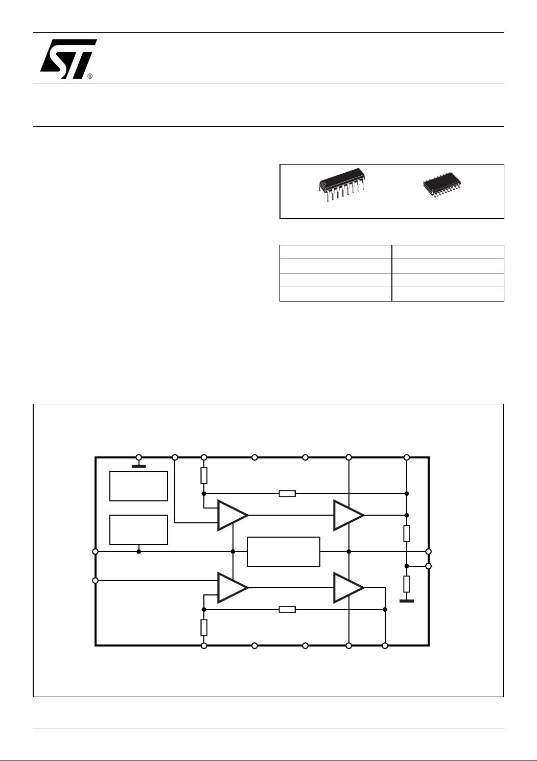
Figure 2. Block Diagram
= 6V, RL = 4Ω
CC
= 9V, RL = 4Ω
CC
= 3V, RL = 4Ω
CC
gure 1. Package
PowerDIP16
SO20
Table 1. Order Codes
Part Number Package
TEA2025B PowerDIP 12+2+2
TEA2025D SO20 12+4+4
TEA2025D013TR SO16 in Tape & Reel
2 DESCRIPTION
The TEA2025B/D is a monolithic integrated circuit
in 12+2+2 Powerdip and 12+4+4 SO, intended for
use as dual or bridge power audio amplifier portable radio cassette players.
OUT 1BOOT 1GNDGNDFEEDIN 1+GND(Sub)
April 2010
SVR
IN 2+
THERMAL
PROTECT.
START
CIRCUIT
D94AU120
50Ω
-
+
2
+
50Ω
FEED GND GND BOOT 2 OUT 2
10KΩ
DECOUPLING
10KΩ
11
5KΩ
2
50Ω
V
S+
BRIDGE
Rev. 3
1/11
TEA2025
Table 2. Absolute Maximum Ratings
Symbol Parameter Value Unit
V
I
O
T
T
stg
Supply Voltage 15 V
S
Ouput Peak Current 1.5 A
Junction Temperature 150 °C
J
Storage Temperature 150 °C
Figure 3. PIN CONNECTION POWERDIP12+2+2
Figure 4. PIN CONNECTION SO12+4+4
FEEDBACK
Table 3. Thermal Data
Symbol Description
R
th j-case
R
th j-amb
Note: 1. The R
Thermal Resistance Junction-case Max 15 15 °C/W
Thermal Resistance Junction-ambient Max 65 60 °C/W
is measured with 4sq cm copper area heatsink
2. The R
th j-amb
is measured on devices bonded on a 10 x 5 x 0.15cm glass-epoxy substrate with a 35µm thick copper surface of 5 cm
th j-amb
BRIDGE
OUT 2
BOOT 2
GND
GND
GND
GND
IN 2(+)
SVR 10 GND(Sub)11
1
2
3
4
5
6
7
8
9 IN 1(+)
D94AU119
20
19
18
17
16
15
14
13
12
V
CC
OUT 1
BOOT 1
GND
GND
GND
GND
FEEDBACK
SO 12+4+4
(1)
PDIP 12+2+2
(2)
Unit
2
2/11
TEA2025
Table 4. Electrical Characteristcs (T
= 25°C, VCC = 9V, Stereo unless otherwise specified)
amb
Symbol Parameter Test Conditions Min. Typ. Max. Unit
V
S
I
Q
V
O
A
V
Supply Voltage 3 12 V
Quiescent Current 35 50 mA
Quiescent Output Voltage 4.5 V
Voltage Gain Stereo 43 45 47 dB
Bridge 49 51 53 dB
∆A
P
R
j
O
Voltage Gain Difference ±1 dB
V
Input Impedance 30 KΩ
Output Power (d = 10%) Stereo 8 (per channel) 9V 4Ω 1.7 2.3 W
9V 8Ω 1.3 W
6V 4Ω 0.7 1 W
6V 8Ω 0.6 W
6V 16Ω 0.25 W
6V 32Ω 0.13 W
3V 4Ω 0.1 W
3V 32Ω 0.02 W
12V 8Ω 2.4 W
Bridge 9V 8Ω 4.7 W
6V 4Ω 2.8 W
6V 8Ω 1.5 W
3V 16Ω 0.18 W
3V 32Ω 0.06 W
dDistortion Vs = 9V; R
SVR Supply Voltage Rejection f = 100Hz, V
E
N(IN)
Input Noise Voltage RG = 0 1.5 3 mV
= 10 4Ω 36mV
R
G
CT Cross-Talk f = 1KHz, R
= 4Ω Stereo
L
Bridge
= 0.5V, Rg = 0 40 46 dB
R
= 10KΩ 40 52 dB
g
0.3
0.5
1.5 %
Table 5.
Te r m . N° (PDIP)1 23456 7 8910111213141516
DC VOLT (V) 0.04 4.5 8.9 0 0 0.6 0.04 8.5 0 0.04 0.6 0 0 8.9 4.5 9
3/11

TEA2025
Figure 5. Bridge Application (Powerdip)
Figure 6. Stereo Application (Powerdip)
Figure 8. Output Voltage vs. Supply Voltage
Figure 9. Output Power vs. Supply Voltage
(THD = 10%, f = 1KHz)
Figure 7. Supply Current vs. Supply Voltage
= 4Ω))
(R
L
4/11
Figure 10. THD versus Output Power (f = 1KHz,
V
= 6V)
S

TEA2025
3 APPLICATION INFORMATION
3.1 Input Capacitor
Input capacitor is PNP type allowing source to be referenced to ground.
In this way no input coupling capacitor is required. However, a series capacitor (0.22 µF)to the input side
can be useful in case of noise due to variable resistor contact.
3.2 Bootstrap
The bootstrap connection allows to increase the output swing.
The suggested value for the bootstrap capacitors (100µF) avoids a reduction of the output signal also at
low frequencies and low supply voltages.
3.3 Voltage Gain Adjust
3.3.1 STEREO MODE
The voltage gain is determined by on-chip resistors R1 and R2 together with the external RfC1 series connected between pin 6 (11) and ground. The frequency response is given approximated
V
OUT
--------------
V
IN
---------------------------------------------=
Rf R2
R1
1
-----------------+÷
JWC1
With Rf=0, C1=100 µF, the gain results 46 dB with pole at f=32 Hz.
THE purpose of Rf is to reduce the gain. It is recommended to not reduce it under 36 dB.
3.3.2 BRIDGE MODE
Figure 11.
The bridge configuration is realized very easily thanks to an internal voltage divider which provides (at pin
1) the CH 1 output signal after reduction.
It is enough to connect pin 6 (inverting input of CH 2) with a capacitor to pin 1 and to connect to ground
the pin 7. The total gain of the bridge is given by:
V
OUT
--------------
V
IN
R1
---------------------------------------------
=
Rf R2
⎛⎞
R3
⎜⎟
------- -
1
+
⎜⎟
1
-----------------+÷
JWC1
R4
⎝⎠
R1
-----------------------------------------------
R2 R4
1
-----------------++
JWC1
and with the suggested values (C1 = C2 = 100 µF, Rf= 0) means: Gv = 52 dB with first pole at f = 32 Hz
5/11

TEA2025
Figure 12.
3.4 Output Capacitors.
The low cut off frequency due to output capacitor depending on the load is given by:
with C
470mF and RL = 4 ohm it means FL = 80 Hz.
OUT
F
L
-----------------------------------=
2ΠC
1
⋅
OUTRL
3.5 Pop Noise
Most amplifiers similar to TEA 2025B need external resistors between DC outputs and ground in order to
optimize the pop on/off performance and crossover distortion.
Figure 13.
The TEA 2025B solution allows to save components because of such resistors (800 ohm)are included into
the chip.
3.6 Stability
A good layout is recommended in order to avoid oscillations.
Generally the designer must pay attention on the following points:
– Short wires of components and short connections.
– No ground loops.
– Bypass of supply voltage with capacitors as nearest as possible to the supply I.C.pin. The low val-
ue(poliester)capacitors must have good temperature and frequency characteristics.
– No sockets.
the heatsink can have a smaller factor of safety compared with that of a conventional circuit. There
is no device damage in the case of excessive junction temperature: all that happens is that PO (and
6/11

TEA2025
therefore Ptot) and Id are reduced.
4 APPLICATION SUGGESTION
The recommended values of the components are those shown on stereo application circuit of Fig. 6 different values can be used, the following table can help the designer.
Table 6.
COMPONENT
C1,C2 0.22µF INPUT DC DECOUPLING
C3 100µF RIPPLE REJECTON DEGRADATION OF
C4,C5 100µF BOOTSTRAP
C6,C7 470µF OUTPUT DC
C8,C9 0.15µF FREQUENCY STABILITY DANGEROF
C10, C11 100µF INVERTING INPUT DC
RECOMMENDED
VALUE
PURPOSE LARGER THAN SMALLER THAN
IN CASE OF SLIDER
CONTACT NOISE OF
VARIABLE RESISTOR
SVR, INCREASE OF AT
LOW FREQUENCY
AND LOW VOLTAGE
INCREASE OF LOW
DECOUPLING
DECOUPLING
FREQUENCY CUTOFF
OSCILLATIONS
INCREASE OFLOW
FREQUENCYCUTOFF
5 PACKAGE MECHANICAL DATA
In order to meet environmental requirements, ST offers these devices in different grades of ECOPACK
packages, depending on their level of environmental compliance. ECOPACK® specifications, grade definitions and product status are available at: www.st.com. ECOPACK
®
is an ST trademark.
®
7/11

TEA2025
Figure 14. SO20 Mechanical Data & Package Dimensions
DIM.
A 2.35 2.65 0.093 0.104
A1 0.10 0.30 0.004 0.012
B 0.33 0.51 0.013 0.200
C 0.23 0.32 0.009 0.013
(1)
12.60 13.00 0.496 0.512
D
E 7.40 7.60 0.291 0.299
e 1.27 0.050
H 10.0 10.65 0.394 0.419
h 0.25 0.75 0.010 0.030
L 0.40 1.27 0.016 0.050
k 0˚ (min.), 8˚ (max.)
ddd 0.10 0.004
(1) “D” dimension does not include mold flash, protusions or gate
burrs. Mold flash, p rotusions or gate burrs shall not exceed
0.15mm per side.
mm inch
MIN. TYP. MAX. MIN. TYP. MAX.
OUTLINE AND
MECHANICAL DATA
SO20
8/11
0016022 D

Figure 15. DIP16 Mechanical Data & Package Dimensions
TEA2025
DIM.
a1 0.51 0.020
B 0.77 1.65 0.030 0.065
b 0.5 0.020
b1 0.25 0.010
D 20 0.787
E 8.5 0.335
e 2.54 0.100
e3 17.78 0.700
F 7.1 0.280
I 5.1 0.201
L 3.3 0.130
Z 1.27 0.050
mm inch
MIN. TYP. MAX. MIN. TYP. MAX.
OUTLINE AND
MECHANICAL DATA
DIP16
9/11

TEA2025
6 REVISION HISTORY
Table 7. Revision History
Date Revision Description of Changes
September 2003 2 Updates not recorded
30-Apr-2010 3 Updated title and added environmental compliance statement for
package
10/11

TEA2025
Please Read Carefully:
Information in this document is provided solely in connection with ST products. STMicroelectronics NV and its subsidiaries (“ST”) reserve the
right to make changes, corrections, modifications or improvements, to this document, and the products and services described herein at any
time, without notice.
All ST products are sold pursuant to ST’s terms and conditions of sale.
Purchasers are solely responsible for the choice, selection and use of the ST products and services described herein, and ST assumes no
liability whatsoever relating to the choice, selection or use of the ST products and services described herein.
No license, express or implied, by estoppel or otherwise, to any intellectual property rights is granted under this document. If any part of this
document refers to any third party products or services it shall not be deemed a license grant by ST for the use of such third party products
or services, or any intellectual property contained therein or considered as a warranty covering the use in any manner whatsoever of such
third party products or services or any intellectual property contained therein.
UNLESS OTHERWISE SET FORTH IN ST’S TERMS AND CONDITIONS OF SALE ST DISCLAIMS ANY EXPRESS OR IMPLIED
WARRANTY WITH RESPECT TO THE USE AND/OR SALE OF ST PRODUCTS INCLUDING WITHOUT LIMITATION IMPLIED
WARRANTIES OF MERCHANTABILITY, FITNESS FOR A PARTICULAR PURPOSE (AND THEIR EQUIVALENTS UNDER THE LAWS
OF ANY JURISDICTION), OR INFRINGEMENT OF ANY PATENT, COPYRIGHT OR OTHER INTELLECTUAL PROPERTY RIGHT.
UNLESS EXPRESSLY APPROVED IN WRITING BY AN AUTHORIZED ST REPRESENTATIVE, ST PRODUCTS ARE NOT
RECOMMENDED, AUTHORIZED OR WARRANTED FOR USE IN MILITARY, AIR CRAFT, SPACE, LIFE SAVING, OR LIFE
SUSTAINING APPLICATIONS, NOR IN PRODUCTS OR SYSTEMS WHERE FAILURE OR MALFUNCTION MAY RESULT IN
PERSONAL INJURY, DEATH, OR SEVERE PROPERTY OR ENVIRONMENTAL DAMAGE. ST PRODUCTS WHICH ARE NOT
SPECIFIED AS "AUTOMOTIVE GRADE" MAY ONLY BE USED IN AUTOMOTIVE APPLICATIONS AT USER’S OWN RISK.
Resale of ST products with provisions different from the statements and/or technical features set forth in this document shall immediately void
any warranty granted by ST for the ST product or service described herein and shall not create or extend in any manner whatsoever, any
liability of ST.
ST and the ST logo are trademarks or registered trademarks of ST in various countries.
Information in this document supersedes and replaces all information previously supplied.
The ST logo is a registered trademark of STMicroelectronics. All other names are the property of their respective owners.
© 2010 STMicroelectronics - All rights reserved
STMicroelectronics group of companies
Australia - Belgium - Brazil - Canada - China - Czech Republic - Finland - France - Germany - Hong Kong - India - Israel - Italy - Japan -
Malaysia - Malta - Morocco - Philippines - Singapore - Spain - Sweden - Switzerland - United Kingdom - United States of America
www.st.com
11/11
 Loading...