

Page 1
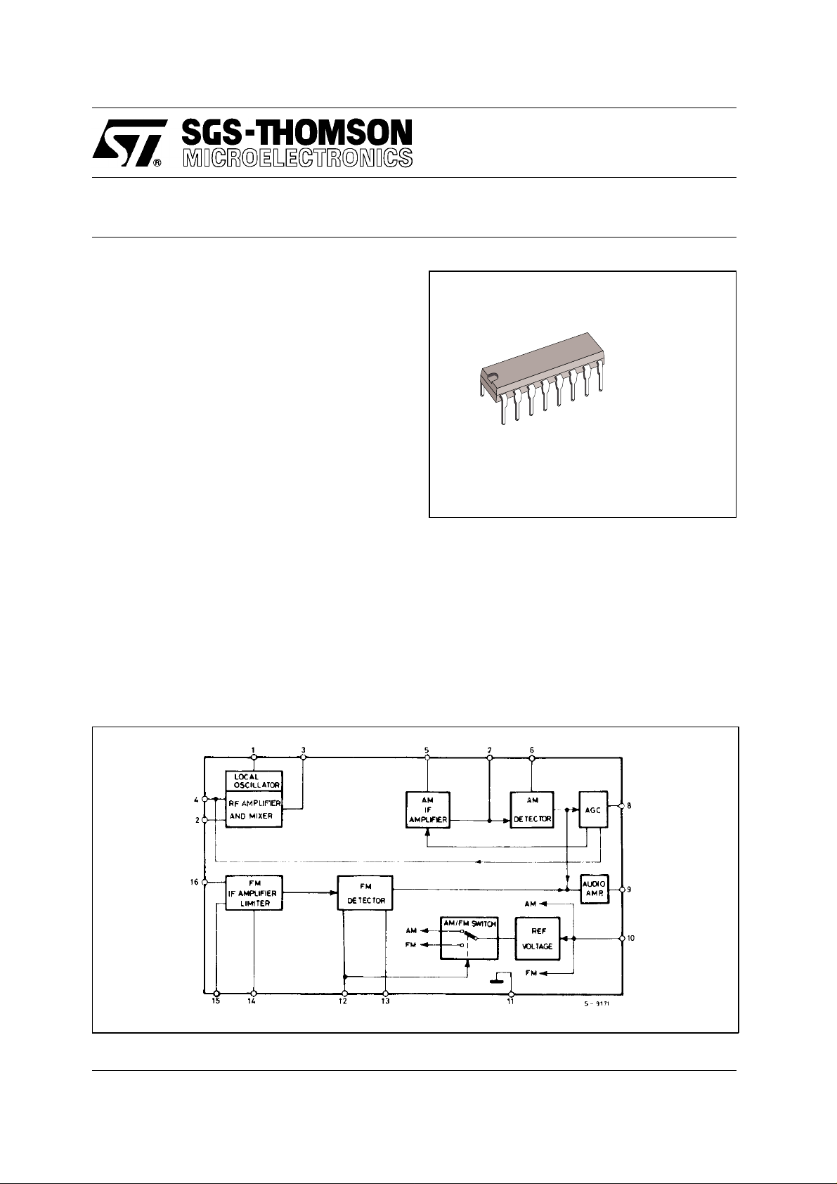
The TDA1220B is a monolithic integrat ed cir cuit i n
a 16-lead dual in-line package.
It is intended for quality receivers produced in large
quantities.
The functions incorporated are:
AM SECTION
– Preamplifier and double balanced mixer
– One pin local oscillat or
– IF amplifier with interna l AGC
– Detector and audio preamplifier
FM SECTION
– IF amplifier and lim iter
– Quadrature detector
– Audio preamplifier
The TDA1220B is suitable up to 30MHz AM and for
FM bands (including 450KHz narrow band) and
features:
– V ery cons tant charact eris tics (3V to 16V)
– High sensitivity and low noise
– V ery low tweet
TDA1220B
AM-FM QUALITY RADIO
DIP-16 Plastic
(0.25)
ORDERING NUMBER : TDA 1220BK
– Sensitivity regulation facility (*)
– High recovered audio signal suited for stereo
decoders and radio recorders
– V ery simple DC s witching of AM -FM
– Low current drain
– AFC facility
(*) Maximum AM sensitivit y can be reduced by means of a resistor
(5 to 12KΩ) between pin 4 and ground.
BLOCK DIAGRAM
March 1993
1/18
Page 2

TDA1220B
ABSOLUTE MAXIMUM RATINGS
Symbol Parameter Value Unit
V
s
P
tot
T
op
T
, T
stg
PIN CONNECTION
(Top view)
Supply voltage 16 V
Total power dissipation at T
< 110°C
amb
400 mW
Operating temperature -20 to 85
Storage and junction temperature -55 to 150
j
°C
°C
THERMAL DATA
Symbol Parameter Value Unit
R
2/18
th-j-amb
Thermal resistance junction-ambient max 100
°C/W
Page 3

TDA1220B
ELECTRICAL CHA RACTERIS TICS ( T
= 25 °C, Vs = 9V unless otherwis e specified, refer to test circuit)
amb
Symbol Parameter Test conditions Min. Typ. Max. Unit
V
Supply voltage 3 16 V
s
Id Drain current FM 10 15 mA
AM 14 20 mA
AM SECTION (f
V
i
= 1 MHz; fm = KHz)
o
Input sensitivity S/N = 26 dB m = 0.3 12 25
S/N Vi = 10 mV m = 0.3 45 52 dB
V
AGC range
i
V
Recovered audio signal
o
= 10 dB
∆V
out
Vi = 1 mV m = 0.3 80 130 200 mV
m = 0.8 94 100 dB
(pin 9)
d Distortion
= 1 mV
V
i
m = 0.3 0.4 1 %
m = 0.8 1.2 %
V
Max input signal handling
H
m = 0.8 d < 10% 1 V
capability
Input resistance between
R
i
m = 0 7.5
pins 2 and 4
Input capacitance between
C
i
m = 0 18 pF
pins 2 and 4
µV
KΩ
R
Output resistance (pin 9) 4.5 7 9.5
o
Tweet 2 IF
m = 0.3 Vi = 1 mV
40 dB
Tweet 3 IF 55 dB
FM SECTION (f
V
i
AMR Amplitude modulation
S/N Ultimate quieting
d Distortion
d Distortion
= 10.8 MHz; fm = 1 KHz)
o
Input limiting voltage -3 dB limiting point 22 36
rejection
∆f = ±22.5 KHz
= 3 mV
V
i
∆f = ±22.5 KHz
∆f = ±75 KHz
∆f = ±22.5 KHz
m = 0.3 40 50 dB
Vi = 1 mV 55 65 dB
= 1 mV 0.7 1.5 %
V
i
V
= 1 mV
i
0.25 0.5 %
d Distortion (double tuned) 0.1 %
V
Recovered audio signal
o
∆f = ±22.5 KHz
Vi = 1 mV 80 110 140 mV
(pin 9)
R
Input resistance between
i
6.5
pin 16 and ground
Ci Input capacitance between
14 pF
pin 16 and ground
R
Output resistance (pin 9) 4.5 7 9.5
o
KΩ
µV
KΩ
KΩ
3/18
Page 4
TDA1220B
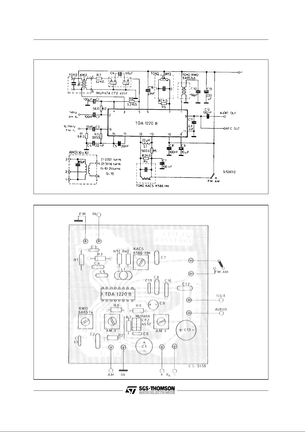
Figure 1. Test circuit
Figure 2. PC board and component layout (1:1 scale) of the test circuit
4/18
Page 5
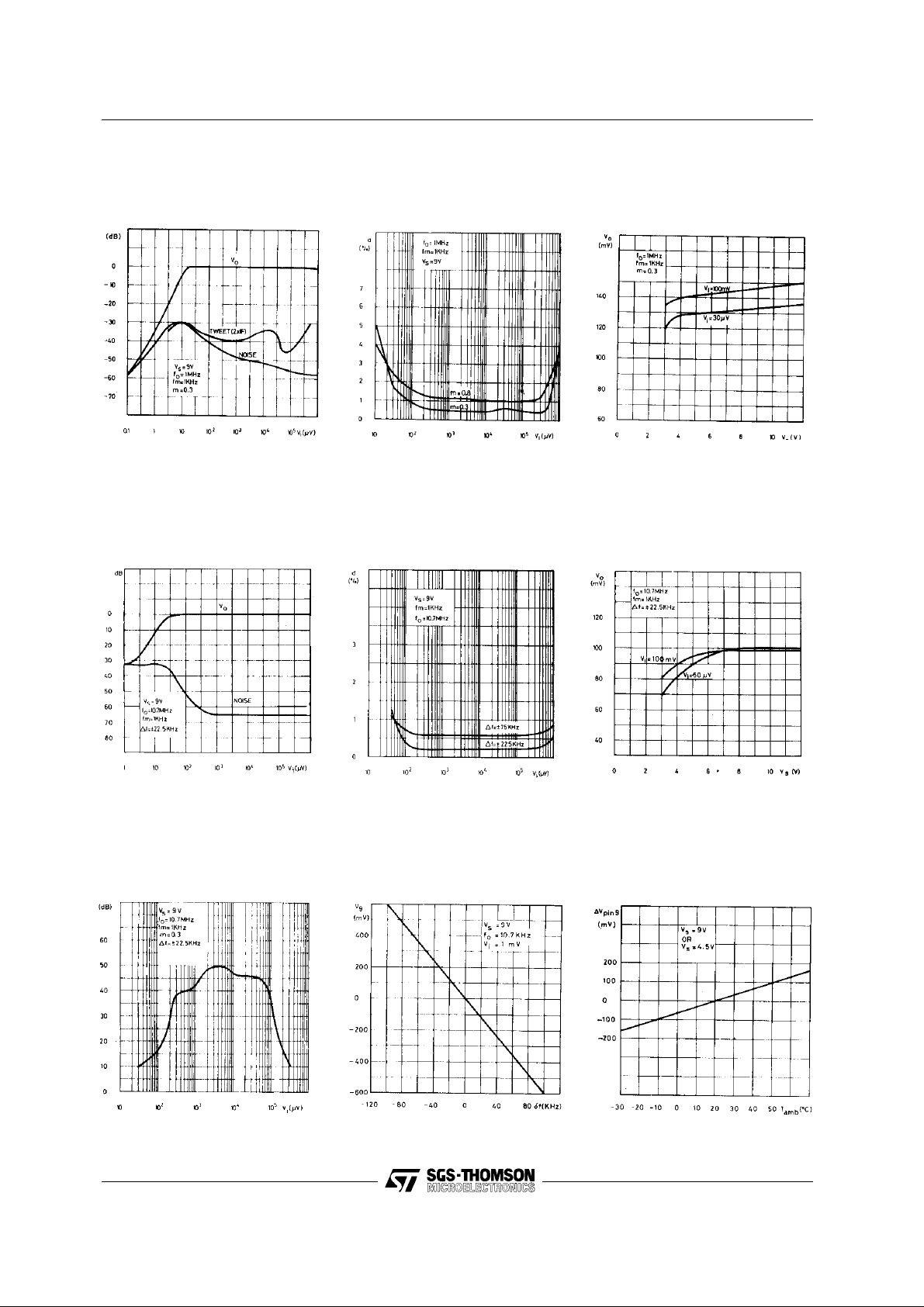
TDA1220B
Figure 3. Audio output, noise
and tweet levels vs. input
signal (AM section)
Figure 6. Audio output and
noise level vs. inpu t signal (FM
section)
Figure 4. Distortion vs. input
signal and modulation index
(AM section)
Figure 7. Distortion vs. input
signal (FM section)
Figure 5. Audio output vs.
supply voltag e (AM sectio n )
Figure 8. Audio output vs.
supply voltag e (F M sectio n )
Figure 9. Amplitude modulation rej ection vs. input signal
(FM section)
Figure 10. ∆ DC output voltage
(pin. 9) vs. frequ ency sh ift (FM
section)
Figure 11. ∆ DC outp ut vo l tag e
(pin 9) vs. ambient
temperature (FM section)
5/18
Page 6

TDA1220B
APPLICATION INFORMATION
AM Section
RF Amplifier and mixer stages
The RF amplifier stage (pin 2) is connected directly to the secondary winding of the ferrite rod antenna or
input tuned circuit. Bias is provided at pin 4 which must be adequately decoupled. The RF amplif ier provides
stable performance ex tending beyond 30 MHz.
The Mixer employed is a double - balanced multiplier and the IF output at pin 3 is connected directly to the
IF filter coil.
Local oscillator
The local oscillator is a cross coupled differential s tage wh ich oscillates at the frequency determined by th e
load on pin 1.
The oscillator resonant circuit is trans former coupled t o pin 1 to improve the Q factor and frequency stability .
The oscillator level at pin 1 is about 100 mV rms and the performance extends beyond 30 MHz, however
to enhance the stability and reduce to a minimum pulling effects of the AGC operation or supply voltage
variations, a high C/L ratio should be used above 10 MHz.
An external oscillator can be injected at pin 1. The level should be 50 mV rms and pin 1 should be connected
to the supply via a 100W resistor .
IF Amplifier Detector
The IF amplifier is a wide band amplifier with a tuned output stage.
The IF filters can be either LC or mixed LC/ceramic.
AM detectio n occurs at pin 7. A detection capacitor is connected t o pin 6 to reduc e the ra diation of spurious
detector products.
The Audio output is at pin 9 (for either AM or FM); the IF frequency is filtered by an external capacitor which
is also used as the FM mono de-enphasis network. The audio output impedance is about 7KΩ and a high
impedance load (~ 50K Ω ) must be used.
AGC
Automatic gain control operates in two ways.
With weak signals it acts on the IF gain, maintaining the maximum S/N. For strong signals a second circuit
intervenes which controls the entire chain and allows signal handling in excess of one volt (m = 0.8).
At pin 8 there is a carrier envelope signal whic h is filtered by an external c apacitor to rem ove the Audio and
RF content and obtain a mean DC signal to drive the AGC circuit.
6/18
Page 7

TDA1220B
APPLICATION INFORMATION (continued)
FM Section
IF Amplifier an d limit e r
The 10.7 MHz IF signal from the ceramic filter is amplified and limited by a chain of four differential stages.
Pin 16 is the amplifier input and has a typical input impedance of 6.5 KW in parallel with 14 pF at 10.7 MHz.
Bias for the first stage is available at pin 14 and provides 100% DC feedback for stable operating conditions.
Pin 15 is the second input to the amplifier and is decoupled to pin 14, which is gro unded by a 20 nF capacitor .
An RLC network is connected to the amplifier output and gives a 9 0° phase shift (at the IF centre frequenc y)
between pins 13 and 12. The signal level at pin 13 is about 150 mV rms
FM Detector
The circuit uses a quadrature detector and t he choise of component values is determined by the acceptable
level of distortion at a given recovered audio level.
With a double tuned network the linearity improves (distortion is reduced) and the phase shift can be
optimized; however this leads to a reduction in the level of the recovered audio. A sat isfactory compr omise
for most FM receiver applications is shown in the test circuit.
Care shoul be taken with the physical layout.
The main recommandations are:
• Locate the phase shift coil as near as possible to pin 13.
• Shunt pins 14 and 16 with a low value resistor (between 56Ω and 330Ω).
• G round the decoupling capacitor of pin 14 and the 10.7 MHz input filter at the same point.
AM-FM Switching
AM-FM switching is achieved by applying a DC voltage at pin 13, to switch the internal reference.
T yp ical DC voltag es (refer to the test circui t)
Pins 1 2 3 4 5 6 7 8 9 10 11 12 13 14 15 16 Unit
AM 9 1.4 9 1.4 1.4 8.4 9 0.7 1.9 9 0 0.1 0.1 8.5 8.5 8.5 V
FM90.0290.020.028.5901.79099888V
7/18
Page 8

TDA1220B
APPLICATION SUGGESTION
Reccomended values are referred to the test circuit of Fig. 2.
Part
number
C1
C2 (*) 100 nF AM input
C3 (*) 10 nF FM input
C4
C5
C6 68 pF Ceramic filter coupling IF bandwidth reduction IF bandwidth increase
C7 100 nF FM detector decoupling Danger of RF irradiation
C8 100 nF Power supply bypass Noise increase of the
C9
C10 (*) 56 pF Tuning of the AM
C11 6.8 nF
C12 100 nF Output DC
Recommended
value
100 µF
20 nF
20 nF
10 µF
Purpose
AGC bypass Increase of the distortion
DC cut
DC cut
FM amplifier bypass Reduction of sensitivity – Bandwidth increase
AGC bypass Increase of the distortion
oscillator at 1455 KHz
50 µs
FM de-enphasis
decoupling
Smaller than
recommended value
at low audio frequency
audio output
at low audio frequency
Low audio frequency cut
Larger than
recommended value
Increase of the AGC time
constant
– Higher noise
Increase of the AGC time
constant
C13
C16 2.7 nF AM detector capacitor Low suppression of
R1 (*) 68 ohm FM input matching
R2 (*) 56 ohm AM input matching
R3 330 ohm Ceramic filter matching Audio output decrease
R4 8.2 Kohm FM detector
R5 560 ohm FM detector
R6 82 Kohm AM detector
R7 2.2 Kohm 455 KHz IF filter
R8 3.3 Kohm 455 KHz IF filter
(*) Only for test circuit
220 µF
Power supply
decoupling
coil Q setting
load resistor
coil Q setting
matching
matching
Increase of the distortion
at low frequency
the IF frequency and
harmonics
and lower distortion
Audio output decrease
and higher AMR
Lower IF gain and Lower
AGC range
Increase of the audio
distortion
Audio output increase
and higher distortion
Higher IF gain and lower
AGC range
8/18
Page 9

APPLICATION INFORMATION (continued)
Figure 12. Port able AM/FM radio
TDA1220B
9/18
Page 10

TDA1220B
APPLICATION INFORMATION (continued)
Figure 13. PC board and component layout of the fig. 12 1 : 1 scale
10/18
Page 11

APPLICATION INFORMATION (continued)
F1 - 10.7 MHz IF Coil
C
o
(pF)
– 1-3 1-2 2-3 4-6
– 10.7 110 6 8 2
f
(MHz)
F3 and F5 - 455 KHz IF Coil
C
o
(pF)
1.3 1-3 1-2 2-3 4-6
180 455 70 57 116 24
f
(KHz)
TDA1220B
Q
o
Q
o
TURNS
TOKO - FM1 - 10x10 mm.
154 AN - 7A5965R
TURNS
TOKO - AM3 - 10x10 mm.
RLC - 4A7525N
F4 - FM Detector Coil
F6 - AM Oscillator Coil
L5 - Antenna Coil
C
o
(pF)
1.3 1-3 1-3 – –
82 10.7 100 12 – –
f
(kHz)
796 220 80 2 75 8
(KHz)
f
(KHz)
L
(µH)
1-3
f
796 105 7
Q
o
Q
o
1-3 1-2 2-3 4-6
L
(µH)
1-2 1-2 1-2 3-4
Q
o
TURNS
TURNS
TURNS
TOKO - 10x10 mm.
KACS - K586 HM
TOKO - 10x10 mm.
RWO + 6A6574N
WIRE: LITZ - 15x0.05 mm.
CORE: 10x80 mm.
11/18
Page 12

TDA1220B
APPLICATION INFORMATION (continued)
Ty pical perfor manc e of the radio receiver of fig. 12 (V
Parameter Test Conditions Value
WAVEBANDS
SENSITIVITY
DISTORTION
(fm = 1KHz)
SIGNAL TO NOISE
(fm = 1KHz)
AMPLITUDE
MODULATION
REJECTION
FM 87.5 to 108 MHz
AM 510 to 1620 KHz
FM S/N = 26dB
AM S/N = 6dB m = 0.3
AM S/N = 26dB m = 0.3
FM P
AM
FM
AM
FM
= 0.5W
o
= 100 µV
V
i
P
= 0.5W
o
= 100 µV
V
i
P
= 0.5W
o
V
= 1 mV
i
V
= 100 µV ∆f = 22.5KHz m = 0.3
i
= 9V)
s
∆f = 22.5KHz 1 µV
1 µV
10 µV
∆f = 22.5KHz
∆f = 75KHz
0.25%
0,7%
m = 0.3 0.4%
m = 0,8 0,8%
∆f = 22.5KHz
64 dB
m = 0.3 50 dB
50 dB
TWEET
2nd H. f = 911 KHz 0.3%
3rd H. f = 1370 KHz 0.07%
QUIESCENT CURRENT 20 mA
SUPPLY VOLTAGE RANGE 3 to 12V
12/18
Page 13

APPLICATION INFORMATION (continued)
Figure 14. Low cost 27 MHz receiver
TDA1220B
Figure 15. L2 Oscil lato r coi l
Coil support: Toko 10K
Primary winding: 10 Turns of enamelled copper wire 0.16 mm diameter (pins 3-1).
Secondary winding: 4 Turns copper wire
0.16 mm diameter (pins 6-4)
Figure 16. L1 An ten na Co il
Coil support: Toko 10K
Primary winding: as L2 (pins 3-1)
Secondary winding: 2 Turns copper wire
0.16 mm diameter (pins 6-4)
Figure 17. Low cost 27 MHz receiver with external xtal oscillat or
13/18
Page 14

TDA1220B
APPLICATION INFORMATION (continued)
Figure 18. 455 KHz FM narrow band IF
Figure 18. P.C. board and component layou t of the circuit of fig. 18
14/18
Page 15

APPLICATION INFORMATION (continued)
Figure 20. Discriminato r "S " cur ve response (ci rcu it of fig. 18)
TDA1220B
Figure 21. Application in sound channel of multistandard TV or in parallel AM modulated sound
channel (AM section on ly).
15/18
Page 16

TDA1220B
ELECTRICAL CHARACTERISTICS (Vs = 12V)
AM Section (f
= 39MHz; fm = 15KHz)
o
Parameter Typ Unit
Audio out (m = 0.3) 60 mV
S/N (V
S/N (V
S/N (V
AGC range (m = 0.8, ∆V
= 100 mV; m = 0.3) 37 dB
i
= 1mV; m = 0.3) 55 dB
i
= 10mV; m = 0.3) 56 dB
i
= 3dB)
out
65 dB
Max input signal handling (m = 0.8; d = 5%) 150 mV
– 3dB bandwidth 600 KHz
Distortion (Vi = 100 µV; m = 0.3)
(V
= 1mV; m = 0.3) 1 %
i
= 10mV; m = 0.3) 0.8 %
(V
i
(V
= 100 µV; m = 0.8)
i
= 1mV; m = 0.8) 5 %
(V
i
= 10mV; m = 0.8) 3 %
(V
i
2%
7%
FM Section (fo = 5.5MHz; fm = 1KHz)
Parameter Typ Unit
–3dB input limiting voltage (∆f = 25KHz)
AMR (∆f = +25KHz; m = 0.3; V
(∆f = +25KHz; m = 0.3; V
(∆f = +25KHz; m = 0.3; V
S/N (∆f = ±25KHz; V
S/N (∆f = ±25KHz; V
S/N (∆f = ±25KHz; V
Distortion (∆f = ±25KHz; V
(∆f = ±25KHz; V
(∆f = ±25KHz; V
(∆f = ±50KHz; V
(∆f = ±50KHz V
(∆f = ±50KHz; V
Recovered audio (∆f = ±15KHz; V
= 100 µV)
i
= 1 mV)
i
= 10mV)
i
= 100 µV)
i
= 1 mV)
i
= 10 mV)
i
= 100 µV)
i
= 1mV)
i
= 10mV)
i
= 1 mV)
i
= 100 µV)
i
= 1mV)
i
= 10mV)
i
3
40 dB
58 dB
54 dB
51 dB
70 dB
70 dB
0.5 %
0.6 %
0.6 %
1%
1%
1%
70 mV
Recovered audio can be varied by variation of 3.3K ohm resistor in parallel with
the discriminator coil)
Max input signal handling 1 V
Note: AM performance at 39MHz can be improved by mean of a selective preamplifier stage.
µV
16/18
Page 17

DIP16 PACKAGE MECHANICA L DATA
TDA1220B
DIM.
MIN. TYP. MAX. MIN. TYP. MAX.
a1 0.51 0.020
B 0.77 1.65 0.030 0.065
b 0.5 0.020
b1 0.25 0.010
D 20 0.787
E 8.5 0.335
e 2.54 0.100
e3 17.78 0.700
F 7.1 0.280
I 5.1 0.201
L 3.3 0.130
Z 1.27 0.050
mm inch
17/18
Page 18

TDA1220B
Information furnished is believed to be accurate and reliable. However, SGS-THOMSON Microelectronics assumes no responsibility for the
consequences of use of such information nor for any infringement of patents or other rights of third parties which may result from its use. No
license is granted by implication or otherwise under any patent or patent rights of SGS -TH OMS O N Microelectronics. Specifications ment ioned
in this publication are subject to change without notice. This publication supersedes and replaces all information previously supplied.
SGS-THOMSON Microelectronics pr oducts are not authorized for use as critical components in life support devices or systems without express
written approval of SGS-THOMSON Microelectronics.
© 1994 SGS-THOMSON Microelectronics - All Rights Reserved
SGS-THOMSON Microelectronics GROUP OF COMPANIES
Australia - Brazil - France - Germany - Hong Kong - Italy - Japan - Korea - Malaysia - Malta - Morocco - The Netherlands - Singapore -
Spain - Sweden - Switzerland - Taiwan - Thaliand - United Kingdom - U.S.A.
18/18
 Loading...