

Wide bandwidth, 2 to 1 HDMI switch with single enable
Features
■ Compatible with HDMI v1.2, DVI v1.0 digital
interfaces
■ 165MHz speed operation supports all video
formats up to 1080p and SXGA (1280 x 1024
at 75Hz)
■ Data rate per channel for UXGA: 1.65Gbps
■ Low R
■ V
CC
■ Low current consumption: 20µA
■ ESD human body model HBM Voltage:
–
■ Channel ON capacitance: 6pF (typ)
■ Switching speed: 9ns
■ Near-zero propagation delay: 250ps
■ Low crosstalk: -32dB at 825MHz
■ Bit-to-bit skew: 200ps
■ Very low ground bounce in flow through mode
■ Data and control inputs provide an undershoot
clamp diode
■ Wide bandwidth minimizes skew and jitter
■ Hot insertion capable
■ Isolated Digital Display Control (DDC) bus for
unused ports
■ 5V tolerance to all DDC and HPD_SINK inputs
■ Supports bi-directional operation
■ Available in the TQFP48 package
■ –40°C to 85°C operating temperature range
: 5.5 Ω(typ)
ON
operating range: 3.135V to 3.465V
±2KV for all I/Os
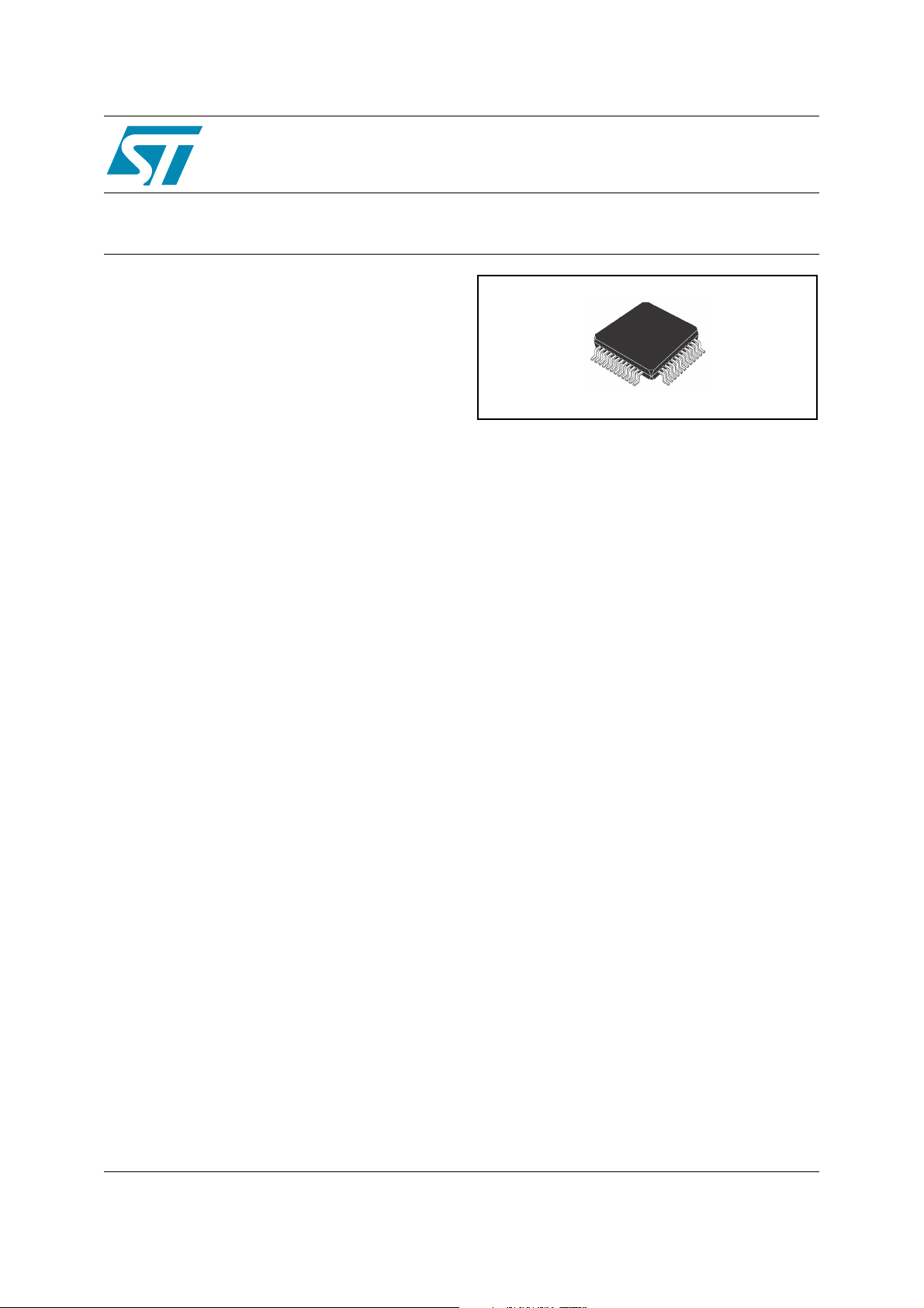
STHDMI002A
TQFP48
Description
The STHDMI002A is a differential Single Pole
Double Throw (SPDT) 2 to 1, low Ron,
bi-directional HDMI switch designed for advanced
TV applications supporting HDMI/DVI which
demand high definition superior image quality.
The differential signal from the 2 ports of HDMI is
multiplexed through the switch to form a single
output HDMI channel going to the HDMI receiver
while the unselected output goes to the high-Z
state.
It is designed for very low cross-talk, low bit-to-bit
skew, high channel-to-channel noise isolation and
low I/O capacitance. The switch offers very little or
practically no attenuation of the high-speed
signals at the outputs, thus preserving the signal
integrity to pass stringent requirements.
The STHDMI002A also includes the DDC as well
as the HPD line switching. The pin layout is
optimized for easy PCB routing to the HDMI
connector and HDMI receivers.
The maximum DVI/HDMI data rate of 1.65Gbps
provides the resolution required by the advanced
HDTV and PC graphics.
Applications
■ Advanced TVs
■ Front projectors
■ LCD TVs
■ PDPs
■ LCD monitors
■ Notebook PCs
■ STB and DVD players
October 2006 Rev 1 1/26
Advantages
STHDMI002A provides the ability to switch a
single source output to various display devices or
switch video display devices between multiple
sources. It reduces the overall BOM costs by
eliminating the need for more costly multi inputoutput controllers.
www.st.com
26

Contents STHDMI002A
Contents
1 Functional diagram . . . . . . . . . . . . . . . . . . . . . . . . . . . . . . . . . . . . . . . . . . . . 4
2 Functional description . . . . . . . . . . . . . . . . . . . . . . . . . . . . . . . . . . . . . . . . . 5
2.1 HPD pins . . . . . . . . . . . . . . . . . . . . . . . . . . . . . . . . . . . . . . . . . . . . . . . . . . . . . 5
2.2 DDC channels . . . . . . . . . . . . . . . . . . . . . . . . . . . . . . . . . . . . . . . . . . . . . . . . . 5
3 Application diagram . . . . . . . . . . . . . . . . . . . . . . . . . . . . . . . . . . . . . . . . . . . 6
4 Pin configuration . . . . . . . . . . . . . . . . . . . . . . . . . . . . . . . . . . . . . . . . . . . . . 7
4.1 Function table . . . . . . . . . . . . . . . . . . . . . . . . . . . . . . . . . . . . . . . . . . . . . . . . 9
5 Maximum rating . . . . . . . . . . . . . . . . . . . . . . . . . . . . . . . . . . . . . . . . . . . . . . 10
6 DC electrical characteristics . . . . . . . . . . . . . . . . . . . . . . . . . . . . . . . . . . . 11
6.1 Capacitance . . . . . . . . . . . . . . . . . . . . . . . . . . . . . . . . . . . . . . . . . . . . . . . . . 13
6.2 Power supply characteristics . . . . . . . . . . . . . . . . . . . . . . . . . . . . . . . . . . . . . 13
6.3 Dynamic electrical characteristics . . . . . . . . . . . . . . . . . . . . . . . . . . . . . . . . . 13
6.4 Dynamic switching characteristics . . . . . . . . . . . . . . . . . . . . . . . . . . . . . . . . 14
6.5 ESD performance . . . . . . . . . . . . . . . . . . . . . . . . . . . . . . . . . . . . . . . . . . . . . 14
7 Test circuit for electrical characteristics . . . . . . . . . . . . . . . . . . . . . . . . . . 15
8 Timing waveforms . . . . . . . . . . . . . . . . . . . . . . . . . . . . . . . . . . . . . . . . . . . . 18
9 Application information . . . . . . . . . . . . . . . . . . . . . . . . . . . . . . . . . . . . . . . 20
9.1 Power supply sequencing . . . . . . . . . . . . . . . . . . . . . . . . . . . . . . . . . . . . . . . 20
2/26

STHDMI002A Contents
9.2 Supply bypassing . . . . . . . . . . . . . . . . . . . . . . . . . . . . . . . . . . . . . . . . . . . . . 20
9.3 Differential traces . . . . . . . . . . . . . . . . . . . . . . . . . . . . . . . . . . . . . . . . . . . . . 20
10 Package mechanical data . . . . . . . . . . . . . . . . . . . . . . . . . . . . . . . . . . . . . . 21
11 Order codes . . . . . . . . . . . . . . . . . . . . . . . . . . . . . . . . . . . . . . . . . . . . . . . . . 24
12 Revision history . . . . . . . . . . . . . . . . . . . . . . . . . . . . . . . . . . . . . . . . . . . . . . 25
3/26
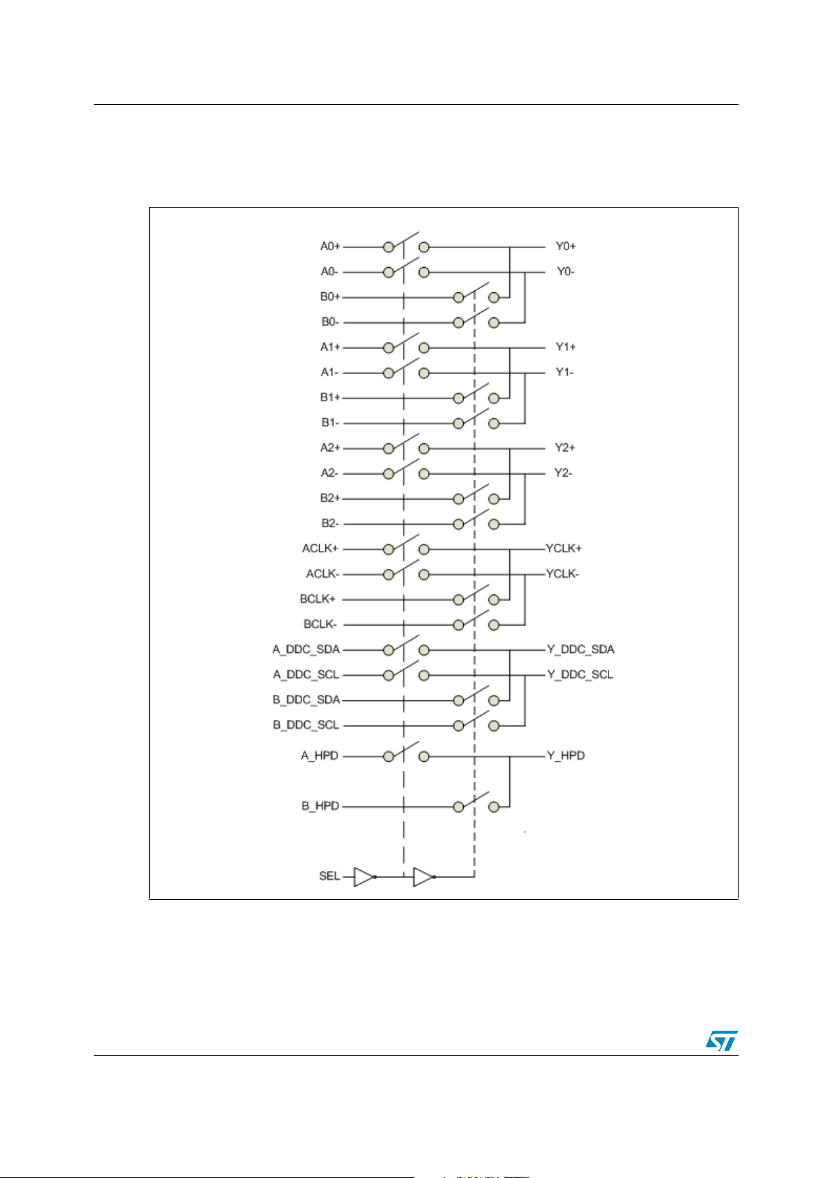
Functional diagram STHDMI002A
1 Functional diagram
Figure 1. Functional diagram
4/26

STHDMI002A Functional description
2 Functional description
The STHDMI002A routes physical layer signals for high bandwidth digital video and is
compatible with low voltage differential signaling standards like TMDS. The device multiplexes
differential outputs from a video source to one of the two corresponding outputs to a common
display. The low on-resistance and low I/O capacitance of STHDMI002A result in a very small
propagation delay. The device integrates SPDT-type switches for 3 differential data TMDS
channels and 1 differential clock channel. Additionally it integrates the switches for DDC and
HPD lines switching.
The I²C interface of the selected input port is linked to the I²C interface of the output port, and
the hot plug detector (HPD) of the selected input port is output to HPD_SINK. For the unused
ports, the I²C interfaces are isolated, and the HPD pins are also isolated.
2.1 HPD pins
The input of the Y_HPD is 5V tolerant, allowing direct connection to 5V signals. The switch is
able to pass both 0V and 5V signal levels. The HPD switch resistance depends on the input
voltage level. At low (near to 0V) input voltage levels, the resistance is 20Ω typically and at high
(near to 5V) input voltage levels, the resistance is 150Ω typically.
2.2 DDC channels
The DDC channels are designed with a bi-directional NMOS gate, providing 5V signal
tolerance. The 5V tolerance allows direct connection to a standard I²C bus, thus eliminating the
need for a level shifter. When the input is a 5V, the NMOS switch is turned off and the pull up
resistor on either side of the switch determines the high voltage potential.
5/26
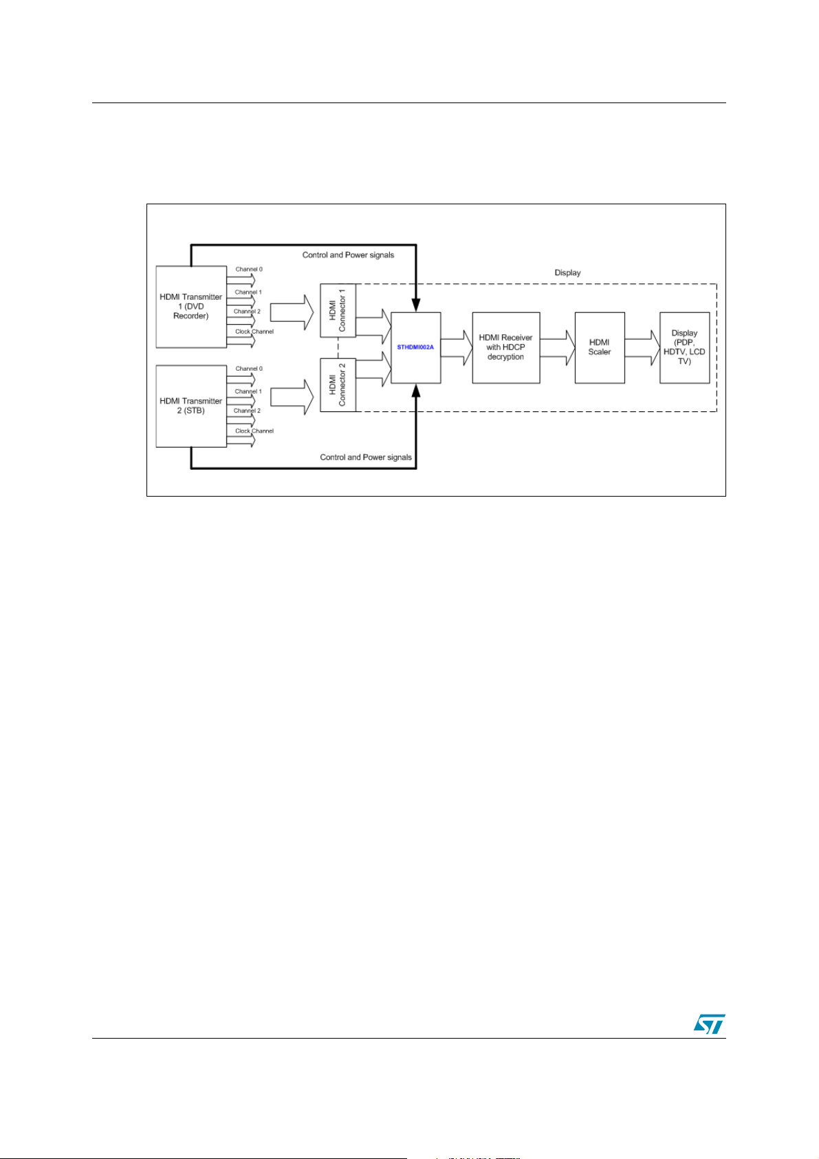
Application diagram STHDMI002A
3 Application diagram
Figure 2. Application diagram
6/26
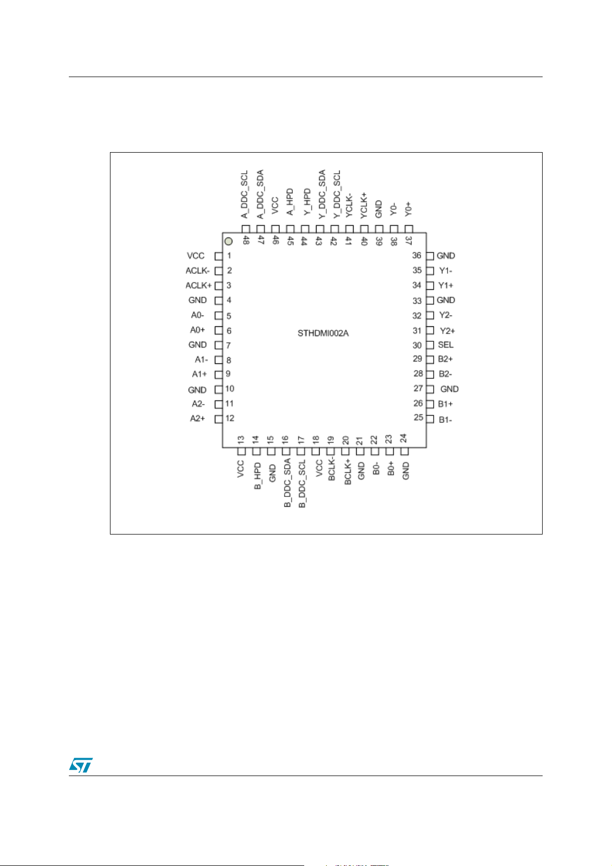
STHDMI002A Pin configuration
4 Pin configuration
Figure 3. Pin connections
TQFP48 (pitch = 0.5mm)
7/26

Pin configuration STHDMI002A
Table 1. Pin description
Pin number Pin Name Type Function
1 VCC Power Supply voltage (3.3V ± 5%)
2 ACLK- Input TMDS Clock- for port A
3 ACLK+ Input TMDS Clock+ for port A
4 GND Power Ground
5 A0- Input TMDS Data 0- for port A
6 A0+ Input TMDS Data 0+ for port A
7 GND Power Ground
8 A1- Input TMDS Data 1- for port A
9 A1+ Input TMDS Data 1+ for port A
10 GND Power Ground
11 A2- Input TMDS Data 2- for port A
12 A2+ Input TMDS Data 2+ for port A
13 VCC Power Supply voltage (3.3V ± 5%)
14 B_HPD Output Hot Plug Detect (HPD) output for port B
15 GND Power Ground
16 B_DDC_SDA I/O DDC SDA input for port B
17 B_DDC_SCL I/O DDC SCL input for port B
18 VCC Power Supply voltage (3.3V ± 5%)
19 BCLK- Input TMDS Clock- for port B
20 BCLK+ Input TMDS Clock+ for port B
21 GND Power Ground
22 B0- Input TMDS Data 0- for port B
23 B0+ Input TMDS Data 0+ for port B
24 GND Power Ground
25 B1- Input TMDS Data 1- for port B
26 B1+ Input TMDS Data 1+ for port B
27 GND Power Ground
28 B2- Input TMDS Data 2- for port B
29 B2+ Input TMDS Data 2+ for port B
30 SEL Input Select control input to select port A or port B
31 Y2+ Output TMDS Data2+ output
32 Y2- Output TMDS Data2- output
33 GND Power Ground
34 Y1+ Output TMDS Data1+ output
8/26

STHDMI002A Pin configuration
Table 1. Pin description
Pin number Pin name Type Function
35 Y1- Output TMDS Data1- output
36 GND Power Ground
37 Y0+ Output TMDS Data0+ output
38 Y0- Output TMDS Data0- output
39 GND Power Ground
40 YCLK+ Output TMDS Clock+ output
41 YCLK- Output TMDS Clock- output
42 Y_DDC_SCL I/O DDC SCL output
43 Y_DDC_SDA I/O DDC SDA output
Sink side hot plug detector input
High : 5V power signal asserted from source to sink
44 Y_HPD Input
45 A_HPD Output Hot Plug Detect (HPD) output for port A
46 VCC Power Supply voltage (3.3V ± 5%)
and EDID is ready
Low : No 5V power signal is asserted from source to
sink or EDID is not ready
47 A_DDC_SDA I/O DDC SDA input for port A
48 A_DDC_SCL I/O DDC SCL input for port A
4.1 Function table
Table 2. Function table
SEL Signal status DDC Status HPD Status
L
H
Y= TMDS Data, Clock for port A
Port B is in ‘Z’ state
Y=TMDS Data, Clock for port B
Port A is in ‘Z’ state
Y = DDC for port A
DDC for port B is ‘Z’
Y = DDC for port B
DDC for port A is ‘Z’
Y= HPD for port A
HPD for port B is ‘Z’
Y= HPD for port B
HPD for port A is ‘Z’
9/26

Maximum rating STHDMI002A
5 Maximum rating
Stressing the device above the rating listed in the “absolute maximum ratings” table may cause
permanent damage to the device. these are stress ratings only and operation of the device at
these or any other conditions above those indicated in the operating sections of this
specification is not implied. Exposure to absolute maximum rating conditions for extended
periods may affect device reliability. Refer also to the STMicroelectronics sure program and
other relevant quality documents.
Table 3. Absolute maximum ratings
Symbol Parameter Value Unit
V
CC
Supply voltage to Ground -0.5 to +4.0 V
DC Input Voltage (TMDS A,B ports) 1.7 to +4.0 V
V
V
I
O
T
STG
T
V
ESD
1. In accordance with the MIL STD 883 method 3015
SEL -0.5 to +4.0 V
I
A_DDC_SDA, A_DDC_SCL, B_DDC_SDA, B_DDC_SCL,
Y_DDC_SDA, Y_DDC_SCL, Y_HPD, A_HPD, B_HPD
DC control input voltage -0.5 to +4.0 V
IC
-0.5 to +6.0 V
DC output current 120 mA
Storage temperature -65 to +150 °C
Lead temperature (10 sec) 300 °C
L
Human body model -2 to +2 kV
Electrostatic discharge voltage on IOs
(1)1
Contact discharge -2 to +2 kV
Table 4. Thermal data
Symbol Description Value Unit
R
thJA
Thermal Resistance Junction-ambient TBA °C/W
10/26

STHDMI002A DC electrical characteristics
6 DC electrical characteristics
TA = -40 to +85 °C, V
= 3.3V ± 5%
CC
Table 5. DC electrical characteristics
Symbol Parameter Test conditions Min Typ Max Unit
I
R
R
∆R
V
V
V
OFF
HIGH level input voltage (SEL pin) High level guaranteed 2.0 V
IH
LOW level input voltage (SEL pin) Low level guaranteed -0.5 0.8 V
IL
Clamp Diode voltage (All IOs)
IK
I
Input high current (SEL pin, A, B data ports)
IH
I
Input low current (SEL pin, A, B data ports)
IL
Power down leakage current
= 3.465V, I
V
CC
= 3.465V, V
V
CC
= 3.465V, V
V
CC
= 0V;
V
CC
Outputs (Y-port) = 0V;
Inputs (A-port) = 3.465V;
= -18mA
IN
= V
IN
= GND
IN
-0.8 -1.2 V
CC
Inputs (B-port) = 3.465V
V
= 3.135 V,
CC
Switch ON resistance
ON
ON resistance flatness
FLAT
(1)
(1) (2)
ON resistance match between channels
ON
∆R
ON
= R
ONMAX
- R
ONMIN
(1) (3)
= 1.5 to V
V
IN
I
= -40mA
IN
V
CC
= 1.5 to V
V
IN
I
= -40mA
IN
V
CC
= 1.5 to V
V
IN
I
= -40mA
IN
CC
= 3.135 V,
CC
= 3.135 V,
CC
±5 µA
±5 µA
±5 µA
5.5 7.5 Ω
0.8 Ω
1.0 1.3 Ω
DDC I/O Pins
I
I(leak)
I
OFF
C
Input leakage current
Power down leakage current
Switch off capacitance
I/O
Switch on capacitance
VCC = 3.465V
V
(max) = 5.3V on
I
isolated DDC ports
Y= 0.0V
= 0V;
V
CC
Outputs (Y-port) = 0V;
Inputs (A-port) = 5.3V;
Inputs (B-port) = 5.3V
=0V, VCC=3.3V, T= 25°C
V
I
F = 1 MHz
0.1 +2 µA
±5 µA
5
9
pF
pF
11/26

DC electrical characteristics STHDMI002A
Table 5. DC electrical characteristics
Symbol Parameter Test conditions Min Typ Max Unit
R
Switch resistance
ON
Status pins (Y_HPD)
I
I(leak)
I
OFF
Input leakage current
Power down leakage current
Status pins (A_HPD, B_HPD)
VCC = 3.3V
I
=3mA; VO=0.0V
O
V
= 3.3V
CC
I
=3mA; VO=0.4V
O
V
= 3.3V
CC
I
=3mA; VO=0.8V
O
V
= 3.3V
CC
I
=3mA; VO=1.5V
O
VCC = 3.465V
V
(max) = 5.3V on
I
isolated HPD port
Y= 0.0V
= 0V;
V
CC
(Y-port) = 0V;
(A-port) = 5.3V;
(B-port) = 5.3V
32 Ω
36 Ω
42 Ω
62 Ω
0.1 +2 µA
±5 µA
=0V, VCC=3.3V, T= 25°C
C
R
1. Measured by voltage drop between channels at the indicated current through the switch. On-resistance is determined by
the lower of the two voltages.
2. Flatness is defined as the difference between the R
3. ∆R
Switch off capacitance
I/O
Switch on capacitance
Switch resistance
ON
measured at the same V
ON
ONMAX
temperature and voltage level.
CC,
V
I
F = 1 MHz
V
CC
=3mA; VO=0.0V
I
O
V
CC
=3mA; VO=5.0V
I
O
and the R
= 3.3V
= 3.3V
of the on resistance over the specified range.
ONMIN
5
9
24 Ω
150 Ω
pF
pF
12/26

STHDMI002A DC electrical characteristics
6.1 Capacitance
TA = 25°C, f = 1MHz
Table 6. Capacitance
Symbol Parameter Test conditions Min Typ Max Unit
C
C
C
1. x = Port Y; x0 = Port A; x1 = Port B
Input capacitance
IN
Port x0 to Port x1, Switch off (Note 4)
OFF
Capacitance switch on (x to x0 or x to x1)
ON
(1)
V
= 0V
IN
V
= 0V
IN
V
= 0V
IN
23pF
46pF
612pF
6.2 Power supply characteristics
TA = -40 to +85 °C
Table 7. Power supply characteristics
Symbol Parameter Test conditions Min Typ Max Unit
V
= 3.465 V,
I
Quiescent power supply current
CC
CC
= V
CC
or GND
V
IN
50 500 µA
6.3 Dynamic electrical characteristics
TA = -40 to +85 °C, V
Table 8. Dynamic electrical characteristics
Symbol Parameter Test conditions Min Typ Max Unit
= 3.3V ± 5%
CC
X
O
TA LK
IRR
Non-adjacent channel Cross-talk
Off Isolation
= 100Ω, f = 370MHz
R
L
R
= 100Ω, f = 825MHz
L
= 100Ω, f = 370MHz
R
L
R
= 100Ω, f = 825MHz
L
-32 dB
-31 dB
-36 dB
-30 dB
BW -3dB bandwidth 850 MHz
D
Data rate per channel 1.65 Gbps
R
13/26

DC electrical characteristics STHDMI002A
6.4 Dynamic switching characteristics
TA = -40 to +85 °C, V
= 3.3V ± 5%
CC
Table 9. Dynamic switching characteristics
Symbol Parameter Test conditions Min Typ Max Unit
V
t
t
PZH, tPZL
t
PHZ, tPLZ
t
SK(O)
t
SK(P)
Propagation delay
PD
Line Enable Time, SEL to x to x0 or x to x1
Line Disable Time, SEL to x to x0 or x to x1
Output skew between center port to any
other port
Skew between opposite transition of the
same output (t
DDC I/O pins
Propagation delay from A_DDC_SDA/
B_DDC_SDA to Y_DDC_SDA or
t
PD(DDC)
A_DDC_SCL/B_DDC_SCL to
Y_DDC_SCL or
Y_DDC_SDA to A_DDC_SDA/
B_DDC_SDA
t
PZH, tPZL
t
PHZ, tPLZ
Line Enable Time, SEL to x to x0 or x to x1
Line Disable Time, SEL to x to x0 or x to x1
PHL
- t
PLH)
= 3.135V to 3.465V
CC
V
= 3.135V to 3.465V
CC
V
= 3.135V to 3.465V
CC
= 3.135V to 3.465V
V
CC
V
= 3.135V to 3.465V
CC
= 10pF
C
L
V
= 3.135V to 3.465V
CC
V
= 3.135V to 3.465V
CC
0.30 ns
0.5 6.5 9 ns
0.5 6.5 8.5 ns
0.1 0.2 ns
0.1 0.2 ns
2.5 ns
6.5 9 ns
6.5 8.5 ns
Status pins (Y_HPD, A_HPD, B_HPD)
t
PD(HPD)
t
PZH, tPZL
t
PHZ, tPLZ
Propagation delay (from Y_HPD to the
active port of HPD)
Line Enable Time, SEL to x to x0 or x to x1
Line Disable Time, SEL to x to x0 or x to x1
CL = 10pF
= 3.135V to 3.465V
V
CC
= 3.135V to 3.465V
V
CC
2.5 ns
6.5 9 ns
6.5 8.5 ns
Note: x = Port Y; x0 = Port A; x1 = Port B
6.5 ESD performance
Table 10. ESD performance
Symbol Parameter Test conditions Min Typ Max Unit
ESD MIL STD 883 method 3015 (all pins) Human Body Model (HBM) ±2kV
14/26

STHDMI002A Test circuit for electrical characteristics
7 Test circuit for electrical characteristics
Figure 4. Timing measurement test circuit
Note: 1 CL = Load capacitance: includes jig and probe capacitance.
2 RT = Termination resistance: should be equal to ZOUT of the Pulse Generator.
Figure 5. Bandwidth measurement test circuit
Note: C
includes probe and jig capacitance
L
Frequency response is measured at the output of the ON channel. For example, when
VSEL = 0 and Y0+ is the input, the output is measured at A0+. All unused analog I/O ports are
left open.
HP8753ES set up:
Average = 4
RBW = 3kHz
VBIAS = 0.35V
ST = 2s
P1 = 0dBm
15/26

Test circuit for electrical characteristics STHDMI002A
Figure 6. Crosstalk measurement test circuit
Note: 1 CL includes probe and jig capacitance
2A 50
Ω
termination resistor is needed to match the loading network analyzer
Crosstalk is measured at the output of the non-adjacent ON channel. For example, when
VSEL = 0, and Y0- is the input, the output is measured at Y1-. All unused analog input ports (Y)
are connected to GND and output ports (A,B) are left open.
HP8753ES set up:
Average = 4
RBW = 3kHz
VBIAS = 0.35V
ST = 2s
P1 = 0dBm
16/26

STHDMI002A Test circuit for electrical characteristics
Figure 7. Off-isolation measurement test circuit
Note: 1 CL includes probe and jig capacitance
2A 50
Ω
termination resistor is needed to match the loading network analyzer
Off-isolation is measured at the output of the OFF channel. For example, when VSEL=0, and
Y0- is the input, the output is measured at B0-. All unused analog input ports (Y) are connected
to GND and output ports (A,B) are left open.
HP8753ES set up:
Average = 4
RBW = 3kHz
VBIAS = 0.35V
ST = 2s
P1 = 0dBm
17/26

Timing waveforms STHDMI002A
8 Timing waveforms
Figure 8. Propagation delay times
Figure 9. Enable and disable times
18/26

STHDMI002A Timing waveforms
Figure 10. Output skew
Figure 11. Pulse skew
19/26

Application information STHDMI002A
9 Application information
9.1 Power supply sequencing
Proper power-supply sequencing is advised for all CMOS devices. It is recommended
to always apply V
9.2 Supply bypassing
Bypass each of the VCC pins with 0.1µF and 1nF capacitors in parallel as close to the device as
possible, with the smaller-valued capacitor as close to the V
9.3 Differential traces
The high-speed TMDS inputs are the most critical parts for the device. There are several
considerations to minimize discontinuities on these transmission lines between the connectors
and the device.
a) Maintain 100-Ω differential transmission line impedance into and out of the
STHDMI002A.
b) Keep an uninterrupted ground plane below the high-speed I/Os.
c) Keep the ground-path vias to the device as close as possible to allow the shortest
return current path.
d) Layout of the TMDS differential inputs should be with the shortest stubs from the
connectors.
before applying any signals to the input/output or control pins.
CC
pin of the device as possible.
CC
Output trace characteristics affect the performance of the STHDMI002A. Use controlled
impedance traces to match trace impedance to both the transmission medium impedance and
termination resistor. Run the differential traces close together to minimize the effects of the
noise. Reduce skew by matching the electrical length of the traces. Avoid discontinuities in the
differential trace layout. Avoid 90 degree turns and minimize the number of vias to further
prevent impedance discontinuities.
20/26

STHDMI002A Package mechanical data
10 Package mechanical data
In order to meet environmental requirements, ST offers these devices in ECOPACK® packages.
These packages have a Lead-free second level interconnect . The category of second Level
Interconnect is marked on the package and on the inner box label, in compliance with JEDEC
Standard JESD97. The maximum ratings related to soldering conditions are also marked on
the inner box label. ECOPACK is an ST trademark. ECOPACK specifications are available at:
www.st.com.
21/26

Package mechanical data STHDMI002A
Figure 12. TQFP48 package dimensions
22/26

STHDMI002A Package mechanical data
Figure 13. TQFP48 Tape and reel dimensions
Tape & Reel TQFP48 MECHANICAL DATA
DIM.
MIN. TYP MAX. MIN. TYP. MAX.
A 330 12.992
C 12.8 13.2 0.504 0.519
D 20.2 0.795
N 60 2.362
T 22.4 0.882
Ao 9.5 9.7 0.374 0.382
Bo 9.5 9.7 0.374 0.382
Ko 2.1 2.3 0.083 0.091
Po 3.9 4.1 0.153 0.161
P 11.9 12.1 0.468 0.476
mm. inch
23/26

Order codes STHDMI002A
11 Order codes
Table 11. Order codes
Part number Temperature range Package Packing
STHDMI002ABTR –65° C to +150° C TQFP48 Tape and reel
24/26

STHDMI002A Revision history
12 Revision history
Table 12. Revision history
Date Revision Change
10-Oct-2006 1 First release
25/26

STHDMI002A
Please Read Carefully:
Information in this document is provided solely in connection with ST products. STMicroelectronics NV and its subsidiaries (“ST”) reserve the
right to make changes, corrections, modifications or improvements, to this document, and the products and services described herein at any
time, without notice.
All ST products are sold pursuant to ST’s terms and conditions of sale.
Purchasers are solely responsible for the choice, selection and use of the ST products and services described herein, and ST assumes no
liability whatsoever relating to the choice, selection or use of the ST products and services described herein.
No license, express or implied, by estoppel or otherwise, to any intellectual property rights is granted under this document. If any part of this
document refers to any third party products or services it shall not be deemed a license grant by ST for the use of such third party products
or services, or any intellectual property contained therein or considered as a warranty covering the use in any manner whatsoever of such
third party products or services or any intellectual property contained therein.
UNLESS OTHERWISE SET FORTH IN ST’S TERMS AND CONDITIONS OF SALE ST DISCLAIMS ANY EXPRESS OR IMPLIED
WARRANTY WITH RESPECT TO THE USE AND/OR SALE OF ST PRODUCTS INCLUDING WITHOUT LIMITATION IMPLIED
WARRANTIES OF MERCHANTABILITY, FITNESS FOR A PARTICULAR PURPOSE (AND THEIR EQUIVALENTS UNDER THE LAWS
OF ANY JURISDICTION), OR INFRINGEMENT OF ANY PATENT, COPYRIGHT OR OTHER INTELLECTUAL PROPERTY RIGHT.
UNLESS EXPRESSLY APPROVED IN WRITING BY AN AUTHORIZED ST REPRESENTATIVE, ST PRODUCTS ARE NOT
RECOMMENDED, AUTHORIZED OR WARRANTED FOR USE IN MILITARY, AIR CRAFT, SPACE, LIFE SAVING, OR LIFE SUSTAINING
APPLICATIONS, NOR IN PRODUCTS OR SYSTEMS WHERE FAILURE OR MALFUNCTION MAY RESULT IN PERSONAL INJURY,
DEATH, OR SEVERE PROPERTY OR ENVIRONMENTAL DAMAGE. ST PRODUCTS WHICH ARE NOT SPECIFIED AS "AUTOMOTIVE
GRADE" MAY ONLY BE USED IN AUTOMOTIVE APPLICATIONS AT USER’S OWN RISK.
Resale of ST products with provisions different from the statements and/or technical features set forth in this document shall immediately void
any warranty granted by ST for the ST product or service described herein and shall not create or extend in any manner whatsoever, any
liability of ST.
ST and the ST logo are trademarks or registered trademarks of ST in various countries.
Information in this document supersedes and replaces all information previously supplied.
The ST logo is a registered trademark of STMicroelectronics. All other names are the property of their respective owners.
© 2006 STMicroelectronics - All rights reserved
STMicroelectronics group of companies
Australia - Belgium - Brazil - Canada - China - Czech Republic - Finland - France - Germany - Hong Kong - India - Israel - Italy - Japan -
Malaysia - Malta - Morocco - Singapore - Spain - Sweden - Switzerland - United Kingdom - United States of America
www.st.com
26/26
 Loading...