

STF715
®
NPN MEDIUM POWER TRANSISTORS
Type Marking
STF715 715
STN715 N715
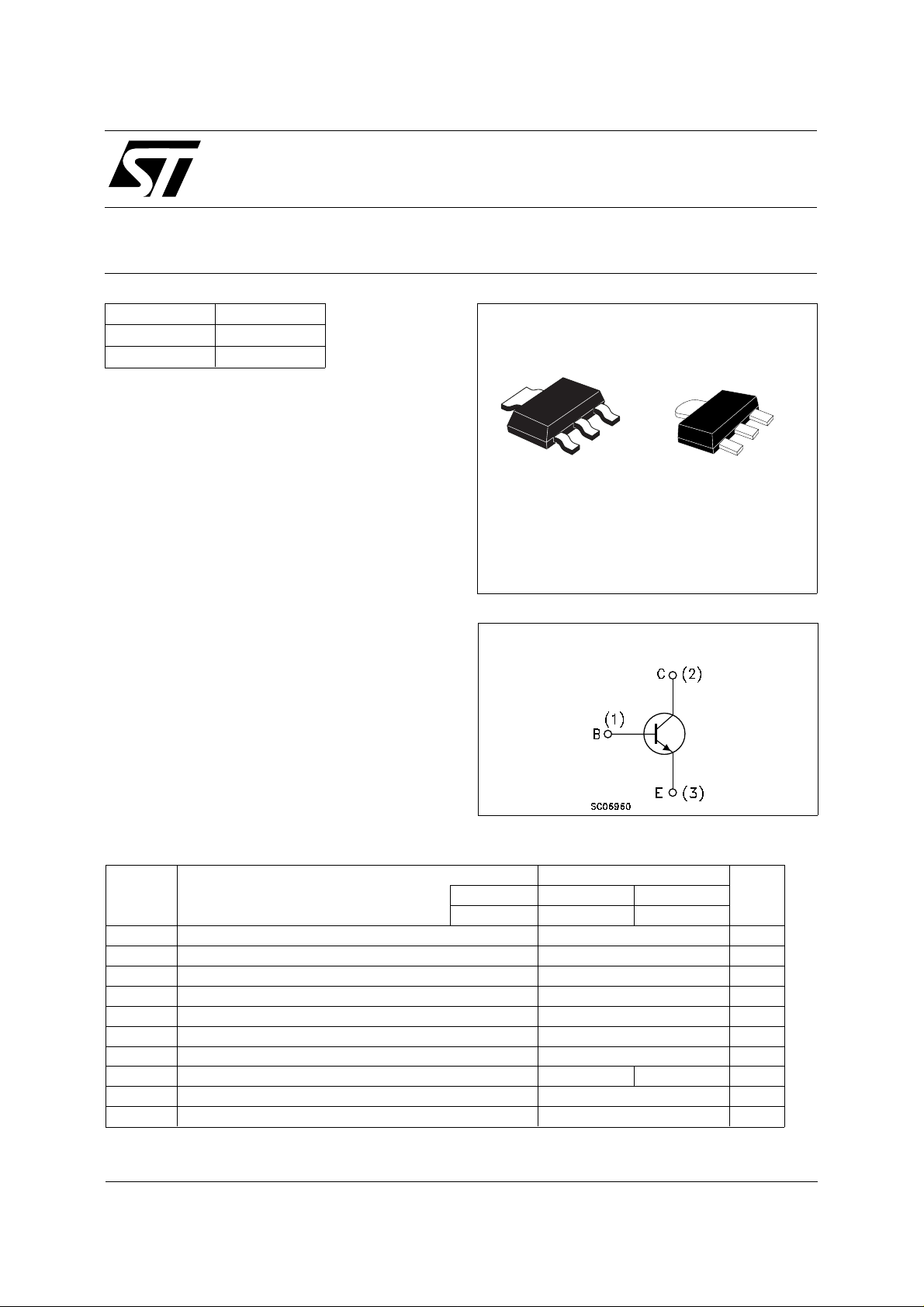
■ SURFACE-MOUNTING DEVICES IN
MEDIUM POWE R SO T-223 AND SO T-89
PACKAGES
■ AVAILABLE IN TAPE & REEL PACKING
APPLICATIONS
■ VOLTAGE REGULATION
■ RELAY DRIVER
■ GENERIC SWITCH
DECRIPTION
The STF715 and STN715 are NPN transistors
manufactured using Planar Technology resulting
in rugged high performance devices.
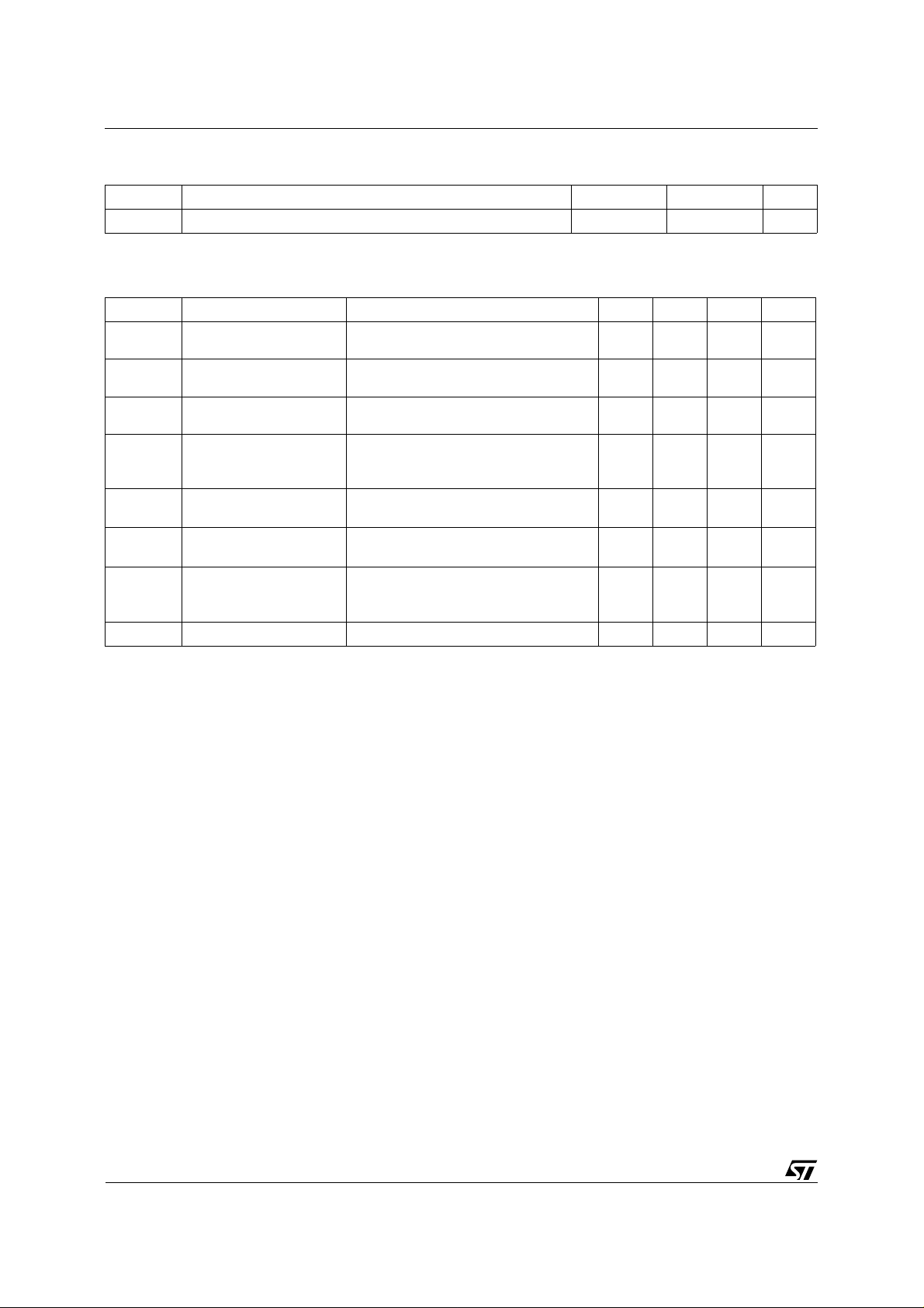
STN715
2
3
2
1
SOT-223
INTERNAL SCHEMATIC DIAGRAM
SOT-89
ABSOL UT E MAXIMU M RATINGS
Symbol Parameter Value Unit
Devices STN715 STF715
Packages SOT-223 SOT-89
V
V
V
I
I
P
T
April 2002
Collector-Base Voltage (IE = 0) 140 V
CBO
Collector-Emitter Voltage (IB = 0) 80 V
CEO
Emitter-Base Voltage (IC = 0) 5 V
EBO
I
Collector Current 1.5 A
C
Collector Peak Current (tp < 5 ms) 2 A
CM
I
Base Current 0.3 A
B
Base Peak Current (tp < 5 ms) 0.6 A
BM
Total Dissipation at Tc = 25 oC 1.6 1.4 W
tot
Storage Temperature -65 to 150
stg
T
Max. Operating Junction Temperature 150
j
o
C
o
C
1/5
STF715 - STN715
THERMAL DATA
R
• Device mounted on a PCB area of 1 cm2.
• Thermal Resistance Junction-ambient Max 78 89
thj-amb
SOT-223 SOT-89
o
C/W
ELECTRICAL CHARACTERISTICS (T
= 25 oC unless otherwise specified)
case
Symbol Parameter Test Conditions Min. Typ. Max. Unit
I
CES
I
CEO
I
EBO
V
CEO(sus)
Collector Cut-off
Current (V
BE
= 0)
Collector Cut-off
Current (I
= 0)
B
Emitter Cut-off Current
(I
= 0)
C
∗ Collector-Emitter
= 140 V 500 µA
V
CE
= 80 V 1 mA
V
CE
= 5 V 100 µA
V
EB
I
= 10 mA 80 V
C
Sustaining Voltage
(I
= 0)
B
V
V
∗ Pulsed: Pulse duration = 300 µs, duty cycle 1.5 %
∗ Collector-Emitter
CE(sat)
Saturation Voltage
∗ Base-Emitter
BE(sat)
Saturation Voltage
h
∗ DC Current Gain IC = 100 mA VCE = 2 V
FE
f
Transition Frequency IC = 0.1 A VCE = 10 V 50 MHz
T
IC = 100 mA IB = 10 mA
I
= 1 A IB = 100 mA
C
IC = 100 mA IB = 10 mA
I
= 1 A IB = 100 mA
C
I
= 500 mA VCE = 2 V
C
I
= 1 A VCE = 2 V
C
0.25
0.5
1
1.1
140
80
40
V
V
V
V
2/5

SOT-223 MECHANICAL DATA
STF715 - STN715
DIM.
MIN. TYP. MAX. MIN. TYP. MAX.
A 1.80 0.071
B 0.60 0.70 0.80 0.024 0.027 0.031
B1 2.90 3.00 3.10 0.114 0.118 0.122
c 0.24 0.2 6 0.32 0.009 0.010 0.013
D 6.30 6.50 6.70 0.248 0.256 0.264
e 2.30 0.090
e1 4.60 0.181
E 3.30 3.50 3.70 0.130 0.138 0.146
H 6.70 7.00 7.30 0.264 0.276 0.287
V10
A1 0.02
mm inch
o
10
o
P008B
3/5

STF715 - STN715
SOT-89 MECHANICAL DATA
DIM.
MIN. TYP. MAX. MIN. TYP. MAX.
A 1.4 1.6 55.1 63.0
B 0.44 0.56 17.3 22.0
B1 0.36 0.48 14.2 18.9
C 0.35 0.44 13.8 17.3
C1 0.35 0.44 13.8 17.3
D 4.4 4.6 173.2 181.1
D1 1.62 1.83 63.8 72.0
E 2.29 2.6 90.2 102.4
e 1.42 1.57 55.9 61.8
e1 2.92 3.07 115.0 120.9
H 3.94 4.25 155.1 167.3
L 0.89 1.2 35.0 47.2
mm mils
4/5
P025H

STF715 - STN715
Information furnished is believed to be accurate and reliable. However, STMicroelectronics assumes no responsibility for the consequences
of use of such inform ation nor for any infringe ment o f patents or other rig hts o f third par ties which ma y resul t from i ts use. N o li cen se is
granted by implicatio n or otherwise un der any patent or patent rights of STMicroelectronics. Specification mentioned in this publication are
subject to change without notice. This publication supersedes and replaces all information previously supplied. STMicroelectronics products
are not authorized for use as critical compo nents in life support devices or systems without express written approval of STMicroelectronics.
The ST logo is a trademark of STMicroelectronics
© 2002 STMicroelectro nics – Printed in Italy – All Rights Reserved
STMicroelectronics GROUP OF COMPANIES
Australia - Brazil - Canada - China - Finland - France - Germany - Hong Kong - India - Israel - Italy - Japan - Malaysia - Malta - Morocco -
Singapore - Spain - Sweden - Switzerland - United Kingdom - United States.
http://www.st.com
5/5
 Loading...