

8-bit MCU with 16 to 60K Flash/ROM, ADC, CSS,
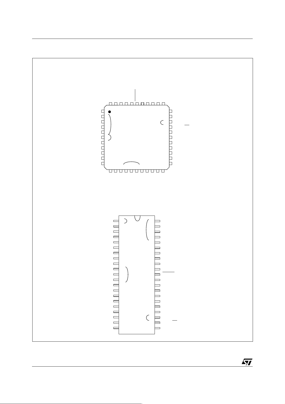
LQFP44
10 x 10
LQFP32
7 x 7
LQFP48
7 x 7
LQFP64
10 x 10
SDIP42
600 mil
SDIP32
400 mil
LQFP64
14 x 14
Features
■ Memories
– 16K to 60K dual voltage High Density Flash
(HDFlash) or up to 32K ROM with read-out
protection capability. In-Application Programming and In-Circuit Programming for HDFlash
devices
– 512 to 2048 bytes RAM
– HDFlash endurance: 100 cycles, data reten-
tion: 40 years at 85°C
■ Clock, reset and supply management
– Enhanced low voltage supervisor (LVD) for
main supply and auxiliary voltage detector
(AVD) with interrupt capability
– Clock sources: crystal/ceramic resonator os-
cillators, internal RC oscillator and bypass for
external clock
– PLL for 2x frequency multiplication
– Four Power Saving Modes: Halt, Active-Halt,
Wait and Slow
– Clock Security System
■ Interrupt management
– Nested interrupt controller
– 14 interrupt vectors plus TRAP and RESET
– Top Level Interrupt (TLI) pin on 64-pin devices
– 9/6 external interrupt lines (on 4 vectors)
■ Up to 48 I/O ports
– 48/36/32/24 multifunctional bidirectional I/O
lines
– 34/26/22/17 alternate function lines
– 16/13/12/10 high sink outputs
■ 5 timers
– Main Clock Controller with: Real time base,
Beep and Clock-out capabilities
ST72325xx
5 timers, SPI, SCI, I
– Configurable watchdog timer
– Two 16-bit timers with: 2 input captures, 2 out-
put compares, external clock input on one timer, PWM and pulse generator modes
– 8-bit PWM Auto-reload timer with: 2 input cap-
tures, 4 PWM outputs, output compare and
time base interrupt, external clock with event
detector
■ 3 Communication interfaces
– SPI synchronous serial interface
– SCI asynchronous serial interface
2
C multimaster interface
–I
■ 1 Analog peripheral (low current coupling)
– 10-bit ADC with up to 16 robust input ports
■ Instruction set
– 8-bit Data Manipulation
– 63 Basic Instructions
– 17 main Addressing Modes
– 8 x 8 Unsigned Multiply Instruction
■ Development tools
– Full hardware/software development package
– DM (Debug module)
2
C interface
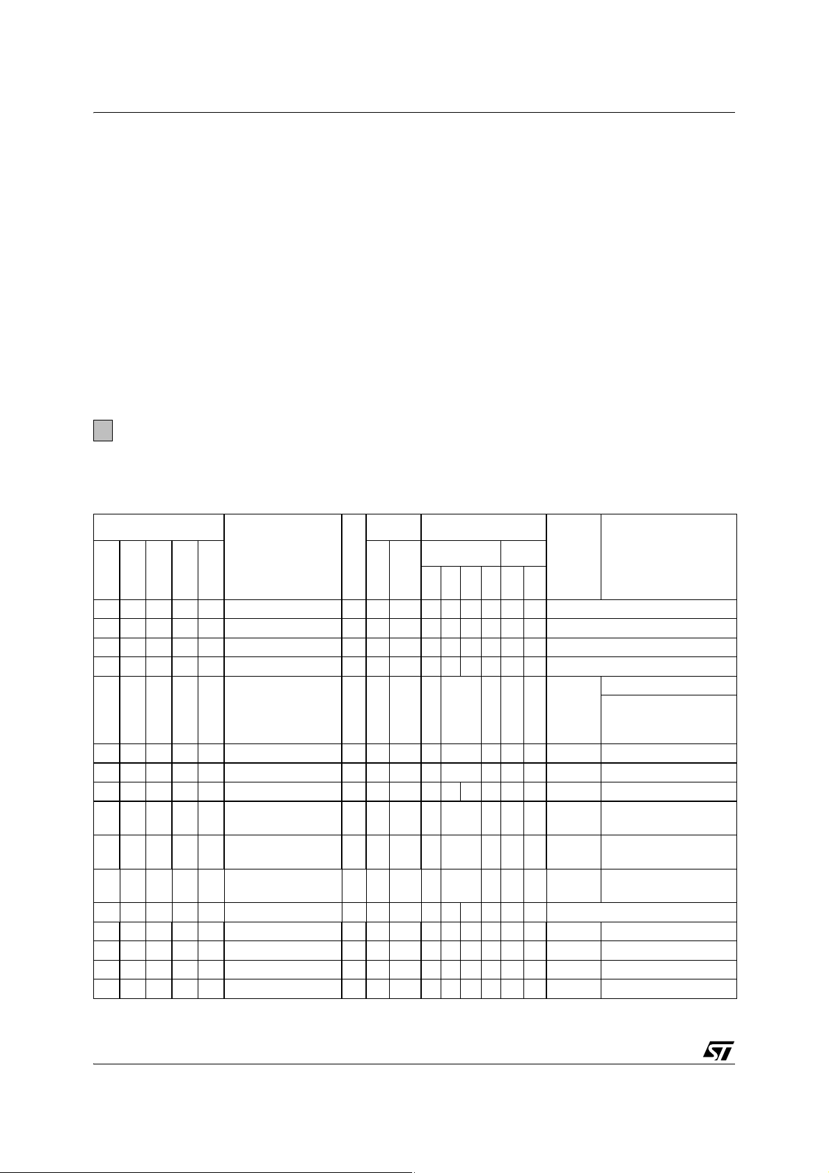
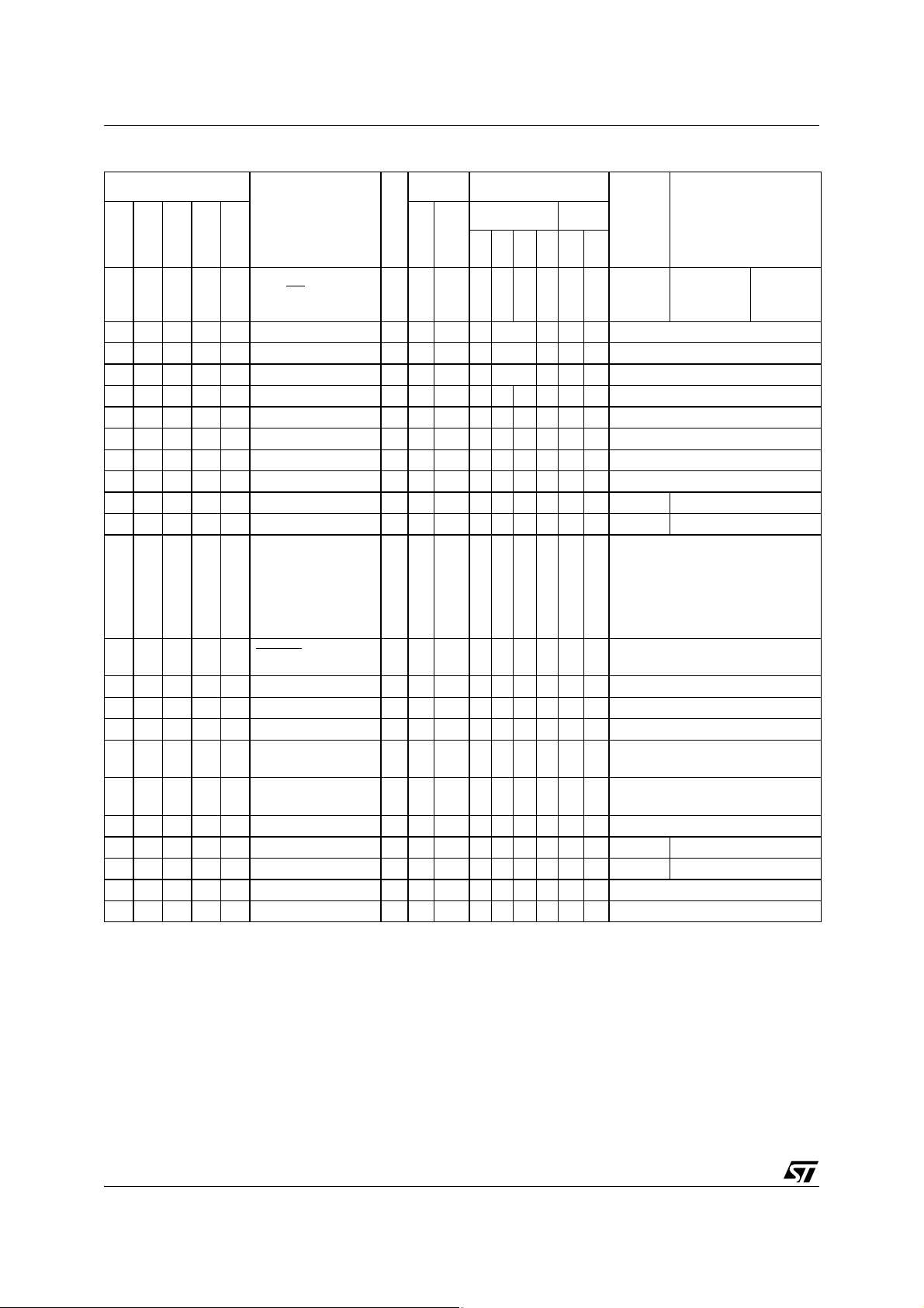
Table 1. Device summary
Features
Program memory - bytes Flash/ROM 16K Flash/ROM 32K Flash 48K Flash 60K
RAM (stack) - bytes 512 (256) 1024(256) 1536 (256) 2048(256)
Operating Voltage 3.8V to 5.5V
Temp. Range up to -40°C to +125°C
Package
October 2008 Rev 4 1/197
LQFP48(S), LQFP44/SDIP42 (J),
ST72325S4 /
ST72325J4 / ST72325K4
LQFP48(S) , LQFP44/ SDIP42 (J),
LQFP32/DIP32 (K)
ST72325S6 /
ST72325J6 / ST72325K6
LQFP32/DIP32 (K)
ST72325J7
LQFP44 (J)
ST72325R9 /
ST72325AR9 /
ST72325C9 /ST72325J9
LQFP64 14x14(R), LQFP64
10x10(AR), LQFP48(C),
LQFP44 (J)
1

Table of Contents
1 DESCRIPTION . . . . . . . . . . . . . . . . . . . . . . . . . . . . . . . . . . . . . . . . . . . . . . . . . . . . . . . . . . . . . . . 7
2 PIN DESCRIPTION . . . . . . . . . . . . . . . . . . . . . . . . . . . . . . . . . . . . . . . . . . . . . . . . . . . . . . . . . . . . 8
3 REGISTER & MEMORY MAP . . . . . . . . . . . . . . . . . . . . . . . . . . . . . . . . . . . . . . . . . . . . . . . . . . . 17
4 FLASH PROGRAM MEMORY . . . . . . . . . . . . . . . . . . . . . . . . . . . . . . . . . . . . . . . . . . . . . . . . . . 21
4.1 INTRODUCTION . . . . . . . . . . . . . . . . . . . . . . . . . . . . . . . . . . . . . . . . . . . . . . . . . . . . . . . . 21
4.2 MAIN FEATURES . . . . . . . . . . . . . . . . . . . . . . . . . . . . . . . . . . . . . . . . . . . . . . . . . . . . . . . 21
4.3 STRUCTURE . . . . . . . . . . . . . . . . . . . . . . . . . . . . . . . . . . . . . . . . . . . . . . . . . . . . . . . . . . . 21
4.3.1 Read-out Protection . . . . . . . . . . . . . . . . . . . . . . . . . . . . . . . . . . . . . . . . . . . . . . . . 21
4.4 ICC INTERFACE . . . . . . . . . . . . . . . . . . . . . . . . . . . . . . . . . . . . . . . . . . . . . . . . . . . . . . . . 22
4.5 ICP (IN-CIRCUIT PROGRAMMING) . . . . . . . . . . . . . . . . . . . . . . . . . . . . . . . . . . . . . . . . . 23
4.6 IAP (IN-APPLICATION PROGRAMMING) . . . . . . . . . . . . . . . . . . . . . . . . . . . . . . . . . . . . . 23
4.7 RELATED DOCUMENTATION . . . . . . . . . . . . . . . . . . . . . . . . . . . . . . . . . . . . . . . . . . . . . 23
4.7.1 Register Description . . . . . . . . . . . . . . . . . . . . . . . . . . . . . . . . . . . . . . . . . . . . . . . 23
5 CENTRAL PROCESSING UNIT . . . . . . . . . . . . . . . . . . . . . . . . . . . . . . . . . . . . . . . . . . . . . . . . . 24
5.1 INTRODUCTION . . . . . . . . . . . . . . . . . . . . . . . . . . . . . . . . . . . . . . . . . . . . . . . . . . . . . . . . 24
5.2 MAIN FEATURES . . . . . . . . . . . . . . . . . . . . . . . . . . . . . . . . . . . . . . . . . . . . . . . . . . . . . . . 24
5.3 CPU REGISTERS . . . . . . . . . . . . . . . . . . . . . . . . . . . . . . . . . . . . . . . . . . . . . . . . . . . . . . . 24
6 SUPPLY, RESET AND CLOCK MANAGEMENT . . . . . . . . . . . . . . . . . . . . . . . . . . . . . . . . . . . . 27
6.1 PHASE LOCKED LOOP . . . . . . . . . . . . . . . . . . . . . . . . . . . . . . . . . . . . . . . . . . . . . . . . . . 27
6.2 MULTI-OSCILLATOR (MO) . . . . . . . . . . . . . . . . . . . . . . . . . . . . . . . . . . . . . . . . . . . . . . . . 28
6.3 RESET SEQUENCE MANAGER (RSM) . . . . . . . . . . . . . . . . . . . . . . . . . . . . . . . . . . . . . . 29
6.3.1 Introduction . . . . . . . . . . . . . . . . . . . . . . . . . . . . . . . . . . . . . . . . . . . . . . . . . . . . . . 29
6.3.2 Asynchronous External RESET pin . . . . . . . . . . . . . . . . . . . . . . . . . . . . . . . . . . . . 29
6.3.3 External Power-On RESET . . . . . . . . . . . . . . . . . . . . . . . . . . . . . . . . . . . . . . . . . . 30
6.3.4 Internal Low Voltage Detector (LVD) RESET . . . . . . . . . . . . . . . . . . . . . . . . . . . . 30
6.3.5 Internal Watchdog RESET . . . . . . . . . . . . . . . . . . . . . . . . . . . . . . . . . . . . . . . . . . 30
6.4 SYSTEM INTEGRITY MANAGEMENT (SI) . . . . . . . . . . . . . . . . . . . . . . . . . . . . . . . . . . . . 31
6.4.1 Low Voltage Detector (LVD) . . . . . . . . . . . . . . . . . . . . . . . . . . . . . . . . . . . . . . . . . 31
6.4.2 Auxiliary Voltage Detector (AVD) . . . . . . . . . . . . . . . . . . . . . . . . . . . . . . . . . . . . . 32
6.4.3 Clock Security System (CSS) . . . . . . . . . . . . . . . . . . . . . . . . . . . . . . . . . . . . . . . . 34
6.4.4 Low Power Modes . . . . . . . . . . . . . . . . . . . . . . . . . . . . . . . . . . . . . . . . . . . . . . . . 34
6.4.5 Register Description . . . . . . . . . . . . . . . . . . . . . . . . . . . . . . . . . . . . . . . . . . . . . . . 35
7 INTERRUPTS . . . . . . . . . . . . . . . . . . . . . . . . . . . . . . . . . . . . . . . . . . . . . . . . . . . . . . . . . . . . . . . 36
7.1 INTRODUCTION . . . . . . . . . . . . . . . . . . . . . . . . . . . . . . . . . . . . . . . . . . . . . . . . . . . . . . . . 36
7.2 MASKING AND PROCESSING FLOW . . . . . . . . . . . . . . . . . . . . . . . . . . . . . . . . . . . . . . . 36
7.3 INTERRUPTS AND LOW POWER MODES . . . . . . . . . . . . . . . . . . . . . . . . . . . . . . . . . . . 38
7.4 CONCURRENT & NESTED MANAGEMENT . . . . . . . . . . . . . . . . . . . . . . . . . . . . . . . . . . 38
7.5 INTERRUPT REGISTER DESCRIPTION . . . . . . . . . . . . . . . . . . . . . . . . . . . . . . . . . . . . . 39
7.6 EXTERNAL INTERRUPTS . . . . . . . . . . . . . . . . . . . . . . . . . . . . . . . . . . . . . . . . . . . . . . . . 41
7.6.1 I/O Port Interrupt Sensitivity . . . . . . . . . . . . . . . . . . . . . . . . . . . . . . . . . . . . . . . . . . 41
7.7 EXTERNAL INTERRUPT CONTROL REGISTER (EICR) . . . . . . . . . . . . . . . . . . . . . . . . . 43
8 POWER SAVING MODES . . . . . . . . . . . . . . . . . . . . . . . . . . . . . . . . . . . . . . . . . . . . . . . . . . . . . 45
8.1 INTRODUCTION . . . . . . . . . . . . . . . . . . . . . . . . . . . . . . . . . . . . . . . . . . . . . . . . . . . . . . . . 45
8.2 SLOW MODE . . . . . . . . . . . . . . . . . . . . . . . . . . . . . . . . . . . . . . . . . . . . . . . . . . . . . . . . . . . 45
197
2/197
1

Table of Contents
8.3 WAIT MODE . . . . . . . . . . . . . . . . . . . . . . . . . . . . . . . . . . . . . . . . . . . . . . . . . . . . . . . . . . . 46
8.4 ACTIVE-HALT AND HALT MODES . . . . . . . . . . . . . . . . . . . . . . . . . . . . . . . . . . . . . . . . . . 47
8.4.1 ACTIVE-HALT MODE . . . . . . . . . . . . . . . . . . . . . . . . . . . . . . . . . . . . . . . . . . . . . . 47
8.4.2 HALT MODE . . . . . . . . . . . . . . . . . . . . . . . . . . . . . . . . . . . . . . . . . . . . . . . . . . . . . 48
9 I/O PORTS . . . . . . . . . . . . . . . . . . . . . . . . . . . . . . . . . . . . . . . . . . . . . . . . . . . . . . . . . . . . . . . . . . 50
9.1 INTRODUCTION . . . . . . . . . . . . . . . . . . . . . . . . . . . . . . . . . . . . . . . . . . . . . . . . . . . . . . . . 50
9.2 FUNCTIONAL DESCRIPTION . . . . . . . . . . . . . . . . . . . . . . . . . . . . . . . . . . . . . . . . . . . . . . 50
9.2.1 Input Modes . . . . . . . . . . . . . . . . . . . . . . . . . . . . . . . . . . . . . . . . . . . . . . . . . . . . . . 50
9.2.2 Output Modes . . . . . . . . . . . . . . . . . . . . . . . . . . . . . . . . . . . . . . . . . . . . . . . . . . . . 50
9.2.3 Alternate Functions . . . . . . . . . . . . . . . . . . . . . . . . . . . . . . . . . . . . . . . . . . . . . . . . 50
9.3 I/O PORT IMPLEMENTATION . . . . . . . . . . . . . . . . . . . . . . . . . . . . . . . . . . . . . . . . . . . . . . 53
9.4 LOW POWER MODES . . . . . . . . . . . . . . . . . . . . . . . . . . . . . . . . . . . . . . . . . . . . . . . . . . . 53
9.5 INTERRUPTS . . . . . . . . . . . . . . . . . . . . . . . . . . . . . . . . . . . . . . . . . . . . . . . . . . . . . . . . . . 53
9.5.1 I/O Port Implementation . . . . . . . . . . . . . . . . . . . . . . . . . . . . . . . . . . . . . . . . . . . . . 54
10 ON-CHIP PERIPHERALS . . . . . . . . . . . . . . . . . . . . . . . . . . . . . . . . . . . . . . . . . . . . . . . . . . . . . 56
10.1 WATCHDOG TIMER (WDG) . . . . . . . . . . . . . . . . . . . . . . . . . . . . . . . . . . . . . . . . . . . . . . . 56
10.1.1 Introduction . . . . . . . . . . . . . . . . . . . . . . . . . . . . . . . . . . . . . . . . . . . . . . . . . . . . . . 56
10.1.2 Main Features . . . . . . . . . . . . . . . . . . . . . . . . . . . . . . . . . . . . . . . . . . . . . . . . . . . . 56
10.1.3 Functional Description . . . . . . . . . . . . . . . . . . . . . . . . . . . . . . . . . . . . . . . . . . . . . . 56
10.1.4 How to Program the Watchdog Timeout . . . . . . . . . . . . . . . . . . . . . . . . . . . . . . . . 57
10.1.5 Low Power Modes . . . . . . . . . . . . . . . . . . . . . . . . . . . . . . . . . . . . . . . . . . . . . . . . . 59
10.1.6 Hardware Watchdog Option . . . . . . . . . . . . . . . . . . . . . . . . . . . . . . . . . . . . . . . . . 59
10.1.7 Using Halt Mode with the WDG (WDGHALT option) . . . . . . . . . . . . . . . . . . . . . . . 59
10.1.8 Interrupts . . . . . . . . . . . . . . . . . . . . . . . . . . . . . . . . . . . . . . . . . . . . . . . . . . . . . . . . 59
10.1.9 Register Description . . . . . . . . . . . . . . . . . . . . . . . . . . . . . . . . . . . . . . . . . . . . . . . 59
10.2 MAIN CLOCK CONTROLLER WITH REAL TIME CLOCK AND BEEPER (MCC/RTC) . . 61
10.2.1 Programmable CPU Clock Prescaler . . . . . . . . . . . . . . . . . . . . . . . . . . . . . . . . . . 61
10.2.2 Clock-out Capability . . . . . . . . . . . . . . . . . . . . . . . . . . . . . . . . . . . . . . . . . . . . . . . . 61
10.2.3 Real Time Clock Timer (RTC) . . . . . . . . . . . . . . . . . . . . . . . . . . . . . . . . . . . . . . . . 61
10.2.4 Beeper . . . . . . . . . . . . . . . . . . . . . . . . . . . . . . . . . . . . . . . . . . . . . . . . . . . . . . . . . . 61
10.2.5 Low Power Modes . . . . . . . . . . . . . . . . . . . . . . . . . . . . . . . . . . . . . . . . . . . . . . . . 62
10.2.6 Interrupts . . . . . . . . . . . . . . . . . . . . . . . . . . . . . . . . . . . . . . . . . . . . . . . . . . . . . . . . 62
10.2.7 Register Description . . . . . . . . . . . . . . . . . . . . . . . . . . . . . . . . . . . . . . . . . . . . . . . 62
10.3 PWM AUTO-RELOAD TIMER (ART) . . . . . . . . . . . . . . . . . . . . . . . . . . . . . . . . . . . . . . . . . 64
10.3.1 Introduction . . . . . . . . . . . . . . . . . . . . . . . . . . . . . . . . . . . . . . . . . . . . . . . . . . . . . . 64
10.3.2 Functional Description . . . . . . . . . . . . . . . . . . . . . . . . . . . . . . . . . . . . . . . . . . . . . . 65
10.3.3 Register Description . . . . . . . . . . . . . . . . . . . . . . . . . . . . . . . . . . . . . . . . . . . . . . . 69
10.4 16-BIT TIMER . . . . . . . . . . . . . . . . . . . . . . . . . . . . . . . . . . . . . . . . . . . . . . . . . . . . . . . . . . 73
10.4.1 Introduction . . . . . . . . . . . . . . . . . . . . . . . . . . . . . . . . . . . . . . . . . . . . . . . . . . . . . . 73
10.4.2 Main Features . . . . . . . . . . . . . . . . . . . . . . . . . . . . . . . . . . . . . . . . . . . . . . . . . . . . 73
10.4.3 Functional Description . . . . . . . . . . . . . . . . . . . . . . . . . . . . . . . . . . . . . . . . . . . . . . 73
10.4.4 Low Power Modes . . . . . . . . . . . . . . . . . . . . . . . . . . . . . . . . . . . . . . . . . . . . . . . . 85
10.4.5 Interrupts . . . . . . . . . . . . . . . . . . . . . . . . . . . . . . . . . . . . . . . . . . . . . . . . . . . . . . . 85
10.4.6 Summary of Timer Modes . . . . . . . . . . . . . . . . . . . . . . . . . . . . . . . . . . . . . . . . . . 85
10.4.7 Register Description . . . . . . . . . . . . . . . . . . . . . . . . . . . . . . . . . . . . . . . . . . . . . . . 86
10.5 SERIAL PERIPHERAL INTERFACE (SPI) . . . . . . . . . . . . . . . . . . . . . . . . . . . . . . . . . . . . 92
3/197
1

Table of Contents
10.5.1 Introduction . . . . . . . . . . . . . . . . . . . . . . . . . . . . . . . . . . . . . . . . . . . . . . . . . . . . . . 92
10.5.2 Main Features . . . . . . . . . . . . . . . . . . . . . . . . . . . . . . . . . . . . . . . . . . . . . . . . . . . . 92
10.5.3 General Description . . . . . . . . . . . . . . . . . . . . . . . . . . . . . . . . . . . . . . . . . . . . . . . . 92
10.5.4 Clock Phase and Clock Polarity . . . . . . . . . . . . . . . . . . . . . . . . . . . . . . . . . . . . . . 96
10.5.5 Error Flags . . . . . . . . . . . . . . . . . . . . . . . . . . . . . . . . . . . . . . . . . . . . . . . . . . . . . . . 97
10.5.6 Low Power Modes . . . . . . . . . . . . . . . . . . . . . . . . . . . . . . . . . . . . . . . . . . . . . . . . . 99
10.5.7 Interrupts . . . . . . . . . . . . . . . . . . . . . . . . . . . . . . . . . . . . . . . . . . . . . . . . . . . . . . . 99
10.5.8 Register Description . . . . . . . . . . . . . . . . . . . . . . . . . . . . . . . . . . . . . . . . . . . . . . 100
10.6 SERIAL COMMUNICATIONS INTERFACE (SCI) . . . . . . . . . . . . . . . . . . . . . . . . . . . . . . 103
10.6.1 Introduction . . . . . . . . . . . . . . . . . . . . . . . . . . . . . . . . . . . . . . . . . . . . . . . . . . . . . 103
10.6.2 Main Features . . . . . . . . . . . . . . . . . . . . . . . . . . . . . . . . . . . . . . . . . . . . . . . . . . . 103
10.6.3 General Description . . . . . . . . . . . . . . . . . . . . . . . . . . . . . . . . . . . . . . . . . . . . . . . 103
10.6.4 Functional Description . . . . . . . . . . . . . . . . . . . . . . . . . . . . . . . . . . . . . . . . . . . . . 105
10.6.5 Low Power Modes . . . . . . . . . . . . . . . . . . . . . . . . . . . . . . . . . . . . . . . . . . . . . . . . 112
10.6.6 Interrupts . . . . . . . . . . . . . . . . . . . . . . . . . . . . . . . . . . . . . . . . . . . . . . . . . . . . . . . 112
10.6.7 Register Description . . . . . . . . . . . . . . . . . . . . . . . . . . . . . . . . . . . . . . . . . . . . . . 113
10.7 I2C BUS INTERFACE (I2C) . . . . . . . . . . . . . . . . . . . . . . . . . . . . . . . . . . . . . . . . . . . . . . . 119
10.7.1 Introduction . . . . . . . . . . . . . . . . . . . . . . . . . . . . . . . . . . . . . . . . . . . . . . . . . . . . . 119
10.7.2 Main Features . . . . . . . . . . . . . . . . . . . . . . . . . . . . . . . . . . . . . . . . . . . . . . . . . . . 119
10.7.3 General Description . . . . . . . . . . . . . . . . . . . . . . . . . . . . . . . . . . . . . . . . . . . . . . . 119
10.7.4 Functional Description . . . . . . . . . . . . . . . . . . . . . . . . . . . . . . . . . . . . . . . . . . . . . 121
10.7.5 Low Power Modes . . . . . . . . . . . . . . . . . . . . . . . . . . . . . . . . . . . . . . . . . . . . . . . . 125
10.7.6 Interrupts . . . . . . . . . . . . . . . . . . . . . . . . . . . . . . . . . . . . . . . . . . . . . . . . . . . . . . . 125
10.7.7 Register Description . . . . . . . . . . . . . . . . . . . . . . . . . . . . . . . . . . . . . . . . . . . . . . 126
10.8 10-BIT A/D CONVERTER (ADC) . . . . . . . . . . . . . . . . . . . . . . . . . . . . . . . . . . . . . . . . . . . 132
10.8.1 Introduction . . . . . . . . . . . . . . . . . . . . . . . . . . . . . . . . . . . . . . . . . . . . . . . . . . . . . 132
10.8.2 Main Features . . . . . . . . . . . . . . . . . . . . . . . . . . . . . . . . . . . . . . . . . . . . . . . . . . . 132
10.8.3 Functional Description . . . . . . . . . . . . . . . . . . . . . . . . . . . . . . . . . . . . . . . . . . . . . 133
10.8.4 Low Power Modes . . . . . . . . . . . . . . . . . . . . . . . . . . . . . . . . . . . . . . . . . . . . . . . . 133
10.8.5 Interrupts . . . . . . . . . . . . . . . . . . . . . . . . . . . . . . . . . . . . . . . . . . . . . . . . . . . . . . . 133
10.8.6 Register Description . . . . . . . . . . . . . . . . . . . . . . . . . . . . . . . . . . . . . . . . . . . . . . 134
11 INSTRUCTION SET . . . . . . . . . . . . . . . . . . . . . . . . . . . . . . . . . . . . . . . . . . . . . . . . . . . . . . . . 136
11.1 CPU ADDRESSING MODES . . . . . . . . . . . . . . . . . . . . . . . . . . . . . . . . . . . . . . . . . . . . . . 136
11.1.1 Inherent . . . . . . . . . . . . . . . . . . . . . . . . . . . . . . . . . . . . . . . . . . . . . . . . . . . . . . . . 137
11.1.2 Immediate . . . . . . . . . . . . . . . . . . . . . . . . . . . . . . . . . . . . . . . . . . . . . . . . . . . . . . 137
11.1.3 Direct . . . . . . . . . . . . . . . . . . . . . . . . . . . . . . . . . . . . . . . . . . . . . . . . . . . . . . . . . . 137
11.1.4 Indexed (No Offset, Short, Long) . . . . . . . . . . . . . . . . . . . . . . . . . . . . . . . . . . . . . 137
11.1.5 Indirect (Short, Long) . . . . . . . . . . . . . . . . . . . . . . . . . . . . . . . . . . . . . . . . . . . . . . 137
11.1.6 Indirect Indexed (Short, Long) . . . . . . . . . . . . . . . . . . . . . . . . . . . . . . . . . . . . . . . 138
11.1.7 Relative mode (Direct, Indirect) . . . . . . . . . . . . . . . . . . . . . . . . . . . . . . . . . . . . . . 138
11.2 INSTRUCTION GROUPS . . . . . . . . . . . . . . . . . . . . . . . . . . . . . . . . . . . . . . . . . . . . . . . . 139
12 ELECTRICAL CHARACTERISTICS . . . . . . . . . . . . . . . . . . . . . . . . . . . . . . . . . . . . . . . . . . . . 142
12.1 PARAMETER CONDITIONS . . . . . . . . . . . . . . . . . . . . . . . . . . . . . . . . . . . . . . . . . . . . . . 142
12.1.1 Minimum and Maximum values . . . . . . . . . . . . . . . . . . . . . . . . . . . . . . . . . . . . . . 142
12.1.2 Typical values . . . . . . . . . . . . . . . . . . . . . . . . . . . . . . . . . . . . . . . . . . . . . . . . . . . 142
12.1.3 Typical curves . . . . . . . . . . . . . . . . . . . . . . . . . . . . . . . . . . . . . . . . . . . . . . . . . . . 142
12.1.4 Loading capacitor . . . . . . . . . . . . . . . . . . . . . . . . . . . . . . . . . . . . . . . . . . . . . . . . 142
12.1.5 Pin input voltage . . . . . . . . . . . . . . . . . . . . . . . . . . . . . . . . . . . . . . . . . . . . . . . . . 142
197
4/197

Table of Contents
12.2 ABSOLUTE MAXIMUM RATINGS . . . . . . . . . . . . . . . . . . . . . . . . . . . . . . . . . . . . . . . . . . 143
12.2.1 Voltage Characteristics . . . . . . . . . . . . . . . . . . . . . . . . . . . . . . . . . . . . . . . . . . . . 143
12.2.2 Current Characteristics . . . . . . . . . . . . . . . . . . . . . . . . . . . . . . . . . . . . . . . . . . . . 143
12.2.3 Thermal Characteristics . . . . . . . . . . . . . . . . . . . . . . . . . . . . . . . . . . . . . . . . . . . 144
12.3 OPERATING CONDITIONS . . . . . . . . . . . . . . . . . . . . . . . . . . . . . . . . . . . . . . . . . . . . . . . 144
12.3.1 General Operating Conditions . . . . . . . . . . . . . . . . . . . . . . . . . . . . . . . . . . . . . . . 144
12.3.2 Operating Conditions with Low Voltage Detector (LVD) . . . . . . . . . . . . . . . . . . . 145
12.3.3 Auxiliary Voltage Detector (AVD) Thresholds . . . . . . . . . . . . . . . . . . . . . . . . . . . 145
12.3.4 External Voltage Detector (EVD) Thresholds . . . . . . . . . . . . . . . . . . . . . . . . . . . 145
12.4 SUPPLY CURRENT CHARACTERISTICS . . . . . . . . . . . . . . . . . . . . . . . . . . . . . . . . . . . 146
12.4.1 CURRENT CONSUMPTION . . . . . . . . . . . . . . . . . . . . . . . . . . . . . . . . . . . . . 146
12.4.2 Supply and Clock Managers . . . . . . . . . . . . . . . . . . . . . . . . . . . . . . . . . . . . . . . . 147
12.4.3 On-Chip Peripherals . . . . . . . . . . . . . . . . . . . . . . . . . . . . . . . . . . . . . . . . . . . . . . 148
12.5 CLOCK AND TIMING CHARACTERISTICS . . . . . . . . . . . . . . . . . . . . . . . . . . . . . . . . . . 149
12.5.1 General Timings . . . . . . . . . . . . . . . . . . . . . . . . . . . . . . . . . . . . . . . . . . . . . . . . . 149
12.5.2 External Clock Source . . . . . . . . . . . . . . . . . . . . . . . . . . . . . . . . . . . . . . . . . . . . 149
12.5.3 Crystal and Ceramic Resonator Oscillators . . . . . . . . . . . . . . . . . . . . . . . . . . . . . 150
12.5.4 RC Oscillators . . . . . . . . . . . . . . . . . . . . . . . . . . . . . . . . . . . . . . . . . . . . . . . . . . . 153
12.5.5 Clock Security System (CSS) . . . . . . . . . . . . . . . . . . . . . . . . . . . . . . . . . . . . . . . 154
12.5.6 PLL Characteristics . . . . . . . . . . . . . . . . . . . . . . . . . . . . . . . . . . . . . . . . . . . . . . . 154
12.6 MEMORY CHARACTERISTICS . . . . . . . . . . . . . . . . . . . . . . . . . . . . . . . . . . . . . . . . . . . 155
12.6.1 RAM and Hardware Registers . . . . . . . . . . . . . . . . . . . . . . . . . . . . . . . . . . . . . . 155
12.6.2 FLASH Memory . . . . . . . . . . . . . . . . . . . . . . . . . . . . . . . . . . . . . . . . . . . . . . . . . 155
12.7 EMC CHARACTERISTICS . . . . . . . . . . . . . . . . . . . . . . . . . . . . . . . . . . . . . . . . . . . . . . . 156
12.7.1 Functional EMS (Electro Magnetic Susceptibility) . . . . . . . . . . . . . . . . . . . . . . . . 156
12.7.2 Electro Magnetic Interference (EMI) . . . . . . . . . . . . . . . . . . . . . . . . . . . . . . . . . . 157
12.7.3 Absolute Maximum Ratings (Electrical Sensitivity) . . . . . . . . . . . . . . . . . . . . . . . 158
12.8 I/O PORT PIN CHARACTERISTICS . . . . . . . . . . . . . . . . . . . . . . . . . . . . . . . . . . . . . . . . 159
12.8.1 General Characteristics . . . . . . . . . . . . . . . . . . . . . . . . . . . . . . . . . . . . . . . . . . . . 159
12.8.2 Output Driving Current . . . . . . . . . . . . . . . . . . . . . . . . . . . . . . . . . . . . . . . . . . . . . 160
12.9 CONTROL PIN CHARACTERISTICS . . . . . . . . . . . . . . . . . . . . . . . . . . . . . . . . . . . . . . . 162
12.9.1 Asynchronous RESET Pin . . . . . . . . . . . . . . . . . . . . . . . . . . . . . . . . . . . . . . . . . . 162
12.9.2 ICCSEL/VPP Pin . . . . . . . . . . . . . . . . . . . . . . . . . . . . . . . . . . . . . . . . . . . . . . . . . 164
12.10TIMER PERIPHERAL CHARACTERISTICS . . . . . . . . . . . . . . . . . . . . . . . . . . . . . . . . . 165
12.10.1 8-Bit PWM-ART Auto-Reload Timer . . . . . . . . . . . . . . . . . . . . . . . . . . . . . . . . . . 165
12.10.2 16-Bit Timer . . . . . . . . . . . . . . . . . . . . . . . . . . . . . . . . . . . . . . . . . . . . . . . . . . . . 165
12.11COMMUNICATION INTERFACE CHARACTERISTICS . . . . . . . . . . . . . . . . . . . . . . . . 166
12.11.1 SPI - Serial Peripheral Interface . . . . . . . . . . . . . . . . . . . . . . . . . . . . . . . . . . . . . 166
12.11.2 I2C - Inter IC Control Interface . . . . . . . . . . . . . . . . . . . . . . . . . . . . . . . . . . . . . . 168
12.1210-BIT ADC CHARACTERISTICS . . . . . . . . . . . . . . . . . . . . . . . . . . . . . . . . . . . . . . . . . 170
12.12.1 Analog Power Supply and Reference Pins . . . . . . . . . . . . . . . . . . . . . . . . . . . . . 172
12.12.2 General PCB Design Guidelines . . . . . . . . . . . . . . . . . . . . . . . . . . . . . . . . . . . . . 172
12.12.3 ADC Accuracy . . . . . . . . . . . . . . . . . . . . . . . . . . . . . . . . . . . . . . . . . . . . . . . . . . . 173
13 PACKAGE CHARACTERISTICS . . . . . . . . . . . . . . . . . . . . . . . . . . . . . . . . . . . . . . . . . . . . . . 174
13.1 PACKAGE MECHANICAL DATA . . . . . . . . . . . . . . . . . . . . . . . . . . . . . . . . . . . . . . . . . . . 174
13.2 THERMAL CHARACTERISTICS . . . . . . . . . . . . . . . . . . . . . . . . . . . . . . . . . . . . . . . . . . 179
5/197

Table of Contents
13.3 SOLDERING INFORMATION . . . . . . . . . . . . . . . . . . . . . . . . . . . . . . . . . . . . . . . . . . . . . 180
14 ST72325 DEVICE CONFIGURATION AND ORDERING INFORMATION . . . . . . . . . . . . . . . 181
14.1 FLASH OPTION BYTES . . . . . . . . . . . . . . . . . . . . . . . . . . . . . . . . . . . . . . . . . . . . . . . . . 181
14.2 DEVICE ORDERING INFORMATION AND TRANSFER OF CUSTOMER CODE . . . . . 183
14.3 DEVELOPMENT TOOLS . . . . . . . . . . . . . . . . . . . . . . . . . . . . . . . . . . . . . . . . . . . . . . . . . 187
14.3.1 Starter kits . . . . . . . . . . . . . . . . . . . . . . . . . . . . . . . . . . . . . . . . . . . . . . . . . . . . . . 187
14.3.2 Development and debugging tools . . . . . . . . . . . . . . . . . . . . . . . . . . . . . . . . . . . 187
14.3.3 Programming tools . . . . . . . . . . . . . . . . . . . . . . . . . . . . . . . . . . . . . . . . . . . . . . . 187
14.3.4 Socket and Emulator Adapter Information . . . . . . . . . . . . . . . . . . . . . . . . . . . . . . 188
14.4 ST7 APPLICATION NOTES . . . . . . . . . . . . . . . . . . . . . . . . . . . . . . . . . . . . . . . . . . . . . . 189
15 KNOWN LIMITATIONS . . . . . . . . . . . . . . . . . . . . . . . . . . . . . . . . . . . . . . . . . . . . . . . . . . . . . . 192
15.1 ALL DEVICES . . . . . . . . . . . . . . . . . . . . . . . . . . . . . . . . . . . . . . . . . . . . . . . . . . . . . . . . . 192
15.1.1 Unexpected Reset Fetch . . . . . . . . . . . . . . . . . . . . . . . . . . . . . . . . . . . . . . . . . . . 192
15.1.2 External interrupt missed . . . . . . . . . . . . . . . . . . . . . . . . . . . . . . . . . . . . . . . . . . . 192
15.1.3 Clearing active interrupts outside interrupt routine . . . . . . . . . . . . . . . . . . . . . . . 193
15.1.4 SCI Wrong Break duration . . . . . . . . . . . . . . . . . . . . . . . . . . . . . . . . . . . . . . . . . . 194
15.1.5 16-bit Timer PWM Mode . . . . . . . . . . . . . . . . . . . . . . . . . . . . . . . . . . . . . . . . . . . 194
15.1.6 TIMD set simultaneously with OC interrupt . . . . . . . . . . . . . . . . . . . . . . . . . . . . . 194
15.1.7 I2C Multimaster . . . . . . . . . . . . . . . . . . . . . . . . . . . . . . . . . . . . . . . . . . . . . . . . . . 194
15.1.8 Pull-up always active on PE2 . . . . . . . . . . . . . . . . . . . . . . . . . . . . . . . . . . . . . . . 195
15.1.9 ADC accuracy 16/32K Flash devices . . . . . . . . . . . . . . . . . . . . . . . . . . . . . . . . . 195
16 REVISION HISTORY . . . . . . . . . . . . . . . . . . . . . . . . . . . . . . . . . . . . . . . . . . . . . . . . . . . . . . . . 196
6/197
197
ST72325xx
8-BIT CORE
ALU
ADDRESS AND DATA BUS
OSC1
V
PP
CONTROL
PROGRAM
(16K - 60K Bytes1))
V
DD
RESET
PORT F
PF7:0
TIMER A
BEEP
RAM
(512 - 2048 Bytes1))
PORT C
10-BIT ADC
V
AREF
V
SSA
PB7:0
PORT E
PE7:0
(2 bits on C/J/K devices)
SCI
TIMER B
PA7:0
(5 bits on C/J devices)
PORT D
PD7:0
SPI
PC7:0
(8 bits)
V
SS
WATCHDOG
OSC
LVD
OSC2
MEMORY
MCC/RTC/BEEP
(4 bits on K devices)
(5 bits on C/J devices)
(3 bits on K devices)
(6 bits on C/J devices)
(2 bits on K devices)
(6 bits on C/J devices)
(5 bits on K devices)
PORT A
PORT B
PWM ART
I2C
EVD
AVD
(8 bits on AR devices)
(8 bits on AR devices)
(8 bits on AR devices)
(8 bits on AR devices)
(8 bits on AR devices)
TLI
1)
ROM devices have up to 32 Kbytes of program memory and up to 1 Kbyte of RAM.
DEBUG MODULE
1 DESCRIPTION
The ST72F325 Flash and ST72325 ROM devices
are members of the ST7 microcontroller family designed for mid-range applications.
They are derivatives of the ST72321 and ST72324
devices, with enhanced characteristics and robust
Clock Security System.
All devices are based on a common industrystandard 8-bit core, featuring an enhanced instruction set and are available with Flash or ROM program memory. The ST7 family architecture offers
both power and flexibility to software developers,
enabling the design of highly efficient and compact
application code.
The on-chip peripherals include an A/D converter,
a PWM Autoreload timer, 2 general purpose tim-
2
C bus, SPI interface and an SCI interface.
ers, I
For power economy, microcontroller can switch
dynamically into WAIT, SLOW, ACTIVE-HALT or
Figure 1. Device Block Diagram
HALT mode when the application is in idle or
stand-by state.
Typical applications are consumer, home, office
and industrial products.
The devices feature an on-chip Debug Module
(DM) to support in-circuit debugging (ICD). For a
description of the DM registers, refer to the ST7
ICC Protocol Reference Manual.
Main Differences with ST72321:
– LQFP48 and LQFP32 packages
– Clock Security System
– Internal RC, Readout protection, LVD and PLL
without limitations
– Negative current injection not allowed on I/O port
PB0 (instead of PC6).
– External interrupts have Exit from Active Halt
mode capability.
7/197
ST72325xx
V
AREF
V
SSA
V
DD_3
V
SS_3
MCO / AIN8 / PF0
BEEP / (HS) PF1
(HS) PF2
OCMP2_A / AIN9 / PF3
OCMP1_A / AIN10 / PF4
ICAP2_A / AIN11 / PF5
ICAP1_A / (HS) PF6
EXTCLK_A / (HS) PF7
AIN4 / PD4
AIN5 / PD5
AIN6 / PD6
AIN7 / PD7
64 63 62 61 60 59 58 57 56 55 54 53 52 51 50 49
48
47
46
45
44
43
42
41
40
39
38
37
36
35
34
33
17 18 19 20 21 22 23 24 29 30 31 3225 26 27 28
1
2
3
4
5
6
7
8
9
10
11
12
13
14
15
16
ei2
ei3
ei0
ei1
PWM3 / PB0
PWM2 / PB1
PWM1 / PB2
PWM0 / PB3
ARTCLK / (HS) PB4
ARTIC1 / PB5
ARTIC2 / PB6
PB7
AIN0 / PD0
AIN1 / PD1
AIN2 / PD2
AIN3 / PD3
(HS) PE4
(HS) PE5
(HS) PE6
(HS) PE7
PA1
PA0
PC7 / SS / AIN15
PC6 / SCK / ICCCLK
PC5 / MOSI / AIN14
PC4 / MISO / ICCDATA
PC3 (HS) / ICAP1_B
PC2 (HS) / ICAP2_B
PC1 / OCMP1_B / AIN13
PC0 / OCMP2_B / AIN12
V
SS_0
V
DD_0
V
SS_1
V
DD_1
PA3 (HS)
PA2
V
DD
_2
OSC1
OSC2
V
SS
_2
TLI
EVD
RESET
V
PP
/ ICCSEL
PA7 (HS) / SCLI
PA6 (HS) / SDAI
PA5 (HS)
PA4 (HS)
PE3
PE2
PE1 / RDI
PE0 / TDO
(HS) 20mA high sink capability
eix associated external interrupt vector
2 PIN DESCRIPTION
Figure 2. 64-Pin LQFP 14x14 and 10x10 Package Pinout
8/197
Figure 3. 48-Pin LQFP 7x7 Device Pinout
44 43 42 41 40 39 38 37
36
35
34
33
32
31
30
29
28
27
26
25
24
23
12
13 14 15 16 17 18 19 20 21 22
1
2
3
4
5
6
7
8
9
10
11
48 47 46 45
AIN4 / PD3
V
DD_0
PC1 / OCMP1_B / AIN13
PC0 / OCMP2_B / AIN12
V
SS_1
V
SS_0
OSC2
V
SS
_2
PA7 (HS) / SCLI
PA6 (HS) / SDAI
PA5 (HS)
PA4 (HS)
PE1/ RDI
PE0 / TDO
V
DD
_2
OSC1
RESET
V
PP
/ICCSEL
PC6 / SCK / ICCCLK
PC5 / MOSI / AIN14
PC4 / MISO / ICCDATA
PC3 (HS) / ICAP1_B
PC2 (HS) / ICAP2_B
V
DD_1
PA3 (HS)
PA2
PC7 / SS / AIN15
V
AREF
V
SSA
MCO / AIN8 / PF0
BEEP / (HS) PF1
(HS) PF2
OCMP1_A / AIN10 / PF4
ICAP1_A / (HS) PF6
EXTCLK_A / (HS) PF7
AIN4 / PD4
AIN5 / PD5
PWM1 / PB2
PWM0 / PB3
ARTCLK / (HS) PB4
ARTIC1 / PB5
AIN0 / PD0
AIN1 / PD1
AIN3 / PD2
PE2
(HS) PE4
PWM3 / PB0
PWM2 / PB1
ei2
ei3
ei0
ei1
eix associated external interrupt vector
(HS) 20mA high sink capability
= Pin not connected in ST72325S devices
Legend
Caution: 48-pin ‘C’ devices have unbonded pins that require software initialization. Refer
to Note 4 on page 16 for details on initializing the I/O registers for these devices.
ST72325xx
9/197
ST72325xx
MCO / AIN8 / PF0
BEEP / (HS) PF1
(HS) PF2
OCMP1_A / AIN10 / PF4
ICAP1_A / (HS) PF6
EXTCLK_A / (HS) PF7
V
DD_0
V
SS_0
AIN5 / PD5
V
AREF
V
SSA
44 43 42 41 40 39 38 37 36 35 34
33
32
31
30
29
28
27
26
25
24
23
12 13 14 15 16 17 18 19 20 21 22
1
2
3
4
5
6
7
8
9
10
11
ei2
ei3
ei0
ei1
PB3
(HS) PB4
AIN0 / PD0
AIN1 / PD1
AIN2 / PD2
AIN3 / PD3
AIN4 / PD4
RDI / PE1
PB0
PB1
PB2
PC6 / SCK / ICCCLK
PC5 / MOSI / AIN14
PC4 / MISO / ICCDATA
PC3 (HS) / ICAP1_B
PC2 (HS) / ICAP2_B
PC1 / OCMP1_B / AIN13
PC0 / OCMP2_B / AIN12
V
SS_1
V
DD_1
PA3 (HS)
PC7 / SS
/ AIN15
V
SS
_2
RESET
V
PP
/ ICCSEL
PA7 (HS) / SCLI
PA6 (HS) / SDAI
PA5 (HS)
PA4 (HS)
PE0 / TDO
V
DD
_2
OSC1
OSC2
38
37
36
35
34
33
32
31
30
29
28
27
16
15
1
2
3
4
5
6
7
8
9
10
11
12
13
14
39
40
41
42
(HS) PB4
AIN0 / PD0
AIN12 / OCMP2_B / PC0
EXTCLK_A / (HS) PF7
ICAP1_A / (HS) PF6
AIN10 / OCMP1_A / PF4
(HS) PF2
BEEP / (HS) PF1
MCO / AIN8 / PF0
AIN5 / PD5
AIN4 / PD4
AIN3 / PD3
AIN2 / PD2
AIN1 / PD1
V
SSA
V
AREF
PB3
PB2
PA4 (HS)
PA5 (HS)
PA6 (HS) / SDAI
PA7 (HS) / SCLI
V
PP
/ ICCSEL
RESET
VSS_2
V
DD
_2
PE0 / TDO
PE1 / RDI
PB0
PB1
OSC1
OSC2
ei3
ei0
ei2
ei1
21
20
17
18
19
AIN14 / MOSI / PC5
ICCDATA / MISO / PC4
ICAP1_B / (HS) PC3
ICAP2_B/ (HS) PC2
AIN13 / OCMP1_B / PC1
26
25
24
23
22
PC6 / SCK / ICCCLK
PC7 / SS
/ AIN15
PA3 (HS)
V
DD_1
V
SS_1
eix associated external interrupt vector
(HS) 20mA high sink capability
Figure 4. 44/42-Pin LQFP Package Pinouts
10/197
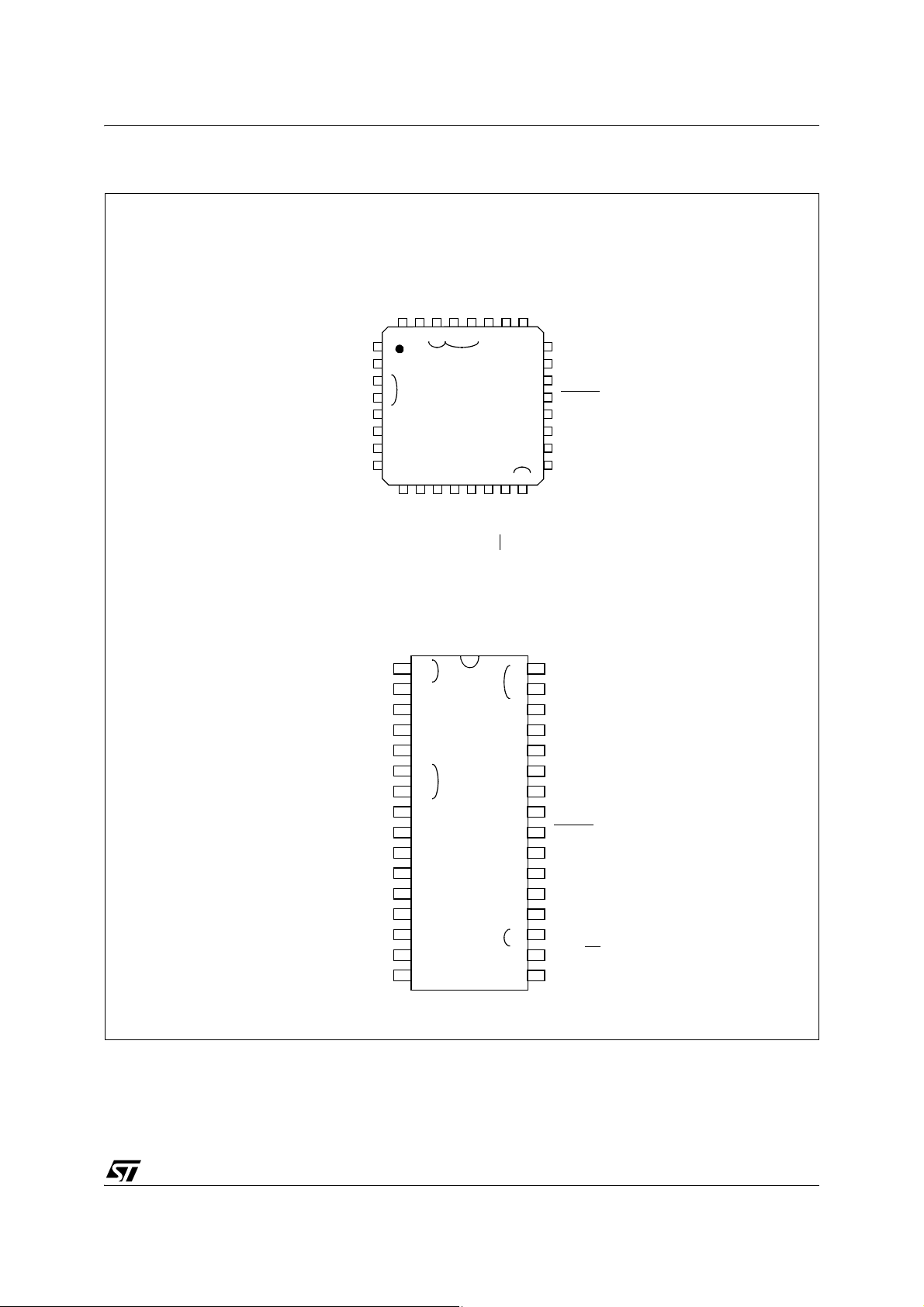
Figure 5. 32-Pin LQFP/DIP Package Pinouts
ICCDATA / MISO / PC4
AIN14 / MOSI / PC5
ICCCLK / SCK / PC6
AIN15 / SS / PC7
(HS) PA3
AIN13 / OCMP1_B / PC1
ICAP2_B / (HS) PC2
ICAP1_B / (HS) PC3
32 31 30 29 28 27 26 25
24
23
22
21
20
19
18
17
9 10111213141516
1
2
3
4
5
6
7
8
ei1
ei3
ei0
OCMP1_A / AIN10 / PF4
ICAP1_A / (HS) PF6
EXTCLK_A / (HS) PF7
AIN12 / OCMP2_B / PC0
V
AREF
V
SSA
MCO / AIN8 / PF0
BEEP / (HS) PF1
V
PP
/ ICCSEL
PA7 (HS)/SCLI
PA6 (HS) / SDAI
PA4 (HS)
OSC1
OSC2
V
SS
_2
RESET
PB0 / PWM3
PE1 / RDI
PE0 / TDO
V
DD
_2
PD1 / AIN1
PD0 / AIN0
PB4 (HS) / ARTCLK
PB3 / PWM0
ei2
28
27
26
25
24
23
22
21
20
19
18
17
16
15
1
2
3
4
5
6
7
8
9
10
11
12
13
14
29
30
31
32
(HS) PB4
AIN0 / PD0
AIN14 / MOSI / PC5
ICCDATA/ MISO / PC4
ICAP1_B / (HS) PC3
ICAP2_B / (HS) PC2
AIN13 / OCMP1_B / PC1
AIN12 / OCMP2_B / PC0
EXTCLK_A / (HS) PF7
BEEP / (HS) PF1
MCO / AIN8 / PF0
V
SSA
V
AREF
AIN1 / PD1
ICAP1_A / (HS) PF6
OCMP1_A / AIN10 / PF4
PB3
PB0
PC6 / SCK / ICCCLK
PC7 / SS / AIN15
PA3 (HS)
PA4 (HS)
PA6 (HS) / SDAI
PA7 (HS) / SCLI
V
PP
/ ICCSEL
OSC2
OSC1
V
DD
_2
PE0 / TDO
PE1 / RDI
VSS_2
RESET
ei0
ei3
ei2
ei1
eix associated external interrupt vector
(HS) 20mA high sink capability
ST72325xx
11/197
ST72325xx
PIN DESCRIPTION (Cont’d)
For external pin connection guidelines, refer to See “ELECTRICAL CHARACTERISTICS” on page 142.
Legend / Abbreviations for Table 2 and Table 3:
Type: I = input, O = output, S = supply
Input level: A = Dedicated analog input
In/Output level: C = CMOS 0.3V
CT= CMOS 0.3VDD/0.7VDD with input trigger
Output level: HS = 20mA high sink (on N-buffer only)
Port and control configuration:
– Input: float = floating, wpu = weak pull-up, int = interrupt
– Output: OD = open drain
Refer to “I/O PORTS” on page 50 for more details on the software configuration of the I/O ports.
The RESET configuration of each pin is shown in bold. This configuration is valid as long as the device is
in reset state.
= Pin not connected in ST72325S devices
Table 2. LQFP64/48/44 and SDIP42 Device Pin Descriptions
/0.7V
DD
2)
DD
, PP = push-pull
1)
, ana = analog
LQFP64
Pin n°
LQFP48S
LQFP48C
Pin Name
SDIP42
LQFP44
Level Port
Type
Input
Output
float
Input Output
int
OD
ana
wpu
Main
function
(after
reset)
PP
Alternate function
12- - -PE4 (HS) I/OCTHS X XXXPort E4
4)
234-
---PE5 (HS) I/OCTHS X XXXPort E5
4)
---PE6 (HS) I/OCTHS X XXXPort E6
4)
---PE7 (HS) I/OCTHS X XXXPort E7
PWM Output 3
533239PB0/PWM3 I/OC
T
X ei2 X X Port B0
Caution: Negative cur-
rent injection not allowed on this pin
644340PB1/PWM2 I/OC
755441PB2/PWM1 I/OC
866542PB3/PWM0 I/OC
9 7 7 6 1 PB4 (HS)/ARTCLK I/O C
10 8 - - - PB5 / ARTIC1 I/O C
4)
11 -
12 -
- - - PB6 / ARTIC2 I/O C
4)
---PB7 I/OCTX ei3 X X Port B7
139972PD0/AIN0 I/OC
14 19 10 8 3 PD1/AIN1 I/O C
15 11 11 9 4 PD2/AIN2 I/O C
16 12 12 10 5 PD3/AIN3 I/O C
T
T
T
T
T
T
T
T
T
T
X ei2 X X Port B1 PWM Output 2
X ei2 X X Port B2 PWM Output 1
X ei2 X X Port B3 PWM Output 0
HS X ei3 X X Port B4
X ei3 X X Port B5
X ei3 X X Port B6
PWM-ART External
Clock
PWM-ART Input Capture 1
PWM-ART Input Capture 2
X X X X X Port D0 ADC Analog Input 0
X X X X X Port D1 ADC Analog Input 1
X X X X X Port D2 ADC Analog Input 2
X X X X X Port D3 ADC Analog Input 3
12/197
ST72325xx
Pin n°
Pin Name
Type
LQFP64
LQFP48S
LQFP48C
SDIP42
LQFP44
17 13 13 11 6 PD4/AIN4 I/O C
18 14 14 12 7 PD5/AIN5 I/O C
4)
19 20 -
21 15 15 13 8 V
22 16 16 14 9 V
23----V
24----V
- - - PD6/AIN6 I/O C
4)
- - - PD7/AIN7 I/O C
6)
AREF
6)
SSA
6)
DD_3
6)
SS_3
I
S Analog Ground Voltage
S Digital Main Supply Voltage
S Digital Ground Voltage
25 17 17 15 10 PF0/MCO/AIN8 I/O C
26 18 18 16 11 PF1 (HS)/BEEP I/O C
27 19 19 17 12 PF2 (HS) I/O C
4)
28 -
---
29 20 20 18 13
4)
30 -
---
PF3/OCMP2_A/
AIN9
PF4/OCMP1_A/
AIN10
PF5/ICAP2_A/
AIN11
I/O C
I/O C
I/O C
31 21 21 19 14 PF6 (HS)/ICAP1_A I/O C
32 22 22 20 15
33 23 23 21 - V
34 24 24 22 - V
35 25 25 23 16
36 26 26 24 17
PF7 (HS)/
EXTCLK_A
6)
DD_0
6)
SS_0
PC0/OCMP2_B/
AIN12
PC1/OCMP1_B/
AIN13
I/O C
S Digital Main Supply Voltage
S Digital Ground Voltage
I/O C
I/O C
37 27 27 25 18 PC2 (HS)/ICAP2_B I/O C
38 28 28 26 19 PC3 (HS)/ICAP1_B I/O C
39 29 29 27 20
PC4/MISO/ICCDATA
I/O C
40 30 30 28 21 PC5/MOSI/AIN14 I/O C
41 31 31 29 22 PC6/SCK/ICCCLK I/O C
Level Port
Input Output
Input
Output
T
T
T
T
X X X X X Port D4 ADC Analog Input 4
X X X X X Port D5 ADC Analog Input 5
X X X X X Port D6 ADC Analog Input 6
X X X X X Port D7 ADC Analog Input 7
float
int
wpu
ana
OD
Main
function
(after
reset)
PP
Alternate function
Analog Reference Voltage for
ADC
/2)
ADC Analog
Input 8
ADC Analog
Input 9
ADC Analog
Input 10
ADC Analog
Input 11
ADC Analog
Input 12
ADC Analog
Input 13
ICC Data
Input
ADC Analog
Input 14
ICC Clock
Output
T
T
T
X ei1 X X X Port F0
HS X ei1 X X Port F1 Beep signal output
HS X ei1 X X Port F2
Main clock
out (f
OSC
Timer A
T
X XXXXPort F3
Output
Compare 2
Timer A
T
X XXXXPort F4
Output
Compare 1
Timer A In-
T
X XXXXPort F5
put Capture 2
HS X X X X Port F6 Timer A Input Capture 1
T
HS X XXXPort F7
T
Timer A External Clock
Source
Timer B
T
X XXXXPort C0
Output
Compare 2
Timer B
T
X XXXXPort C1
Output
Compare 1
HS X X X X Port C2 Timer B Input Capture 2
T
HS X X X X Port C3 Timer B Input Capture 1
T
SPI Master
T
X XXXPort C4
In / Slave
Out Data
SPI Master
T
X XXXXPort C5
Out / Slave
In Data
T
X XXXPort C6
SPI Serial
Clock
13/197
ST72325xx
LQFP64
Pin n°
LQFP48S
LQFP48C
Pin Name
SDIP42
LQFP44
Level Port
Type
Input
Output
float
Input Output
int
OD
ana
wpu
Main
function
(after
reset)
PP
Alternate function
SPI Slave
42 32 32 30 23 PC7/SS/AIN15 I/O C
T
X XXXXPort C7
Select (active low)
4)
43 44 45 33 - - - PA2 I/O C
46 34 34 31 24 PA3 (HS) I/O C
47 35 35 32 25 V
48 36 36 33 26 V
49 37 37 34 27 PA4 (HS) I/O C
50 38 38 35 28 PA5 (HS) I/O C
51 39 39 36 29 PA6 (HS)/SDAI I/O C
52 40 40 37 30 PA7 (HS)/SCLI I/O CTHS X TPort A7 I
---PA0 I/OCTX ei0 X X Port A0
4)
---PA1 I/OCTX ei0 X X Port A1
X ei0 X X Port A2
HS X ei0 X X Port A3
HS X XXXPort A4
HS X XXXPort A5
HS X TPort A6 I
DD_1
SS_1
T
6)
6)
T
S Digital Main Supply Voltage
S Digital Ground Voltage
T
T
T
2
C Data
2
C Clock
1)
1)
Must be tied low. In flash programming mode, this pin acts as the
53 41 41 38 31 VPP/ ICCSEL I
programming voltage input V
See Section 12.9.2 for more details. High voltage must not be applied to ROM devices
54 42 42 39 32 RESET
I/O C
T
Top priority non maskable inter-
rupt.
55 - - - - EVD External voltage detector
56----TLI IC
57 43 43 40 33 V
58 44 44 41 34 OSC2
59 45 45 42 35 OSC1
60 46 46 43 36 V
SS_2
DD_2
6)
3)
3)
6)
61 47 47 44 37 PE0/TDO I/O C
62 48 48 1 38 PE1/RDI I/O C
63 1 - - - PE2 I/O C
4)
64 -
---PE3 I/OCTX XXXPort E3
T
S Digital Ground Voltage
I/O
I
S Digital Main Supply Voltage
T
T
T
X Top level interrupt input pin
Resonator oscillator inverter out-
put
External clock input or Resonator
oscillator inverter input
X X X X Port E0 SCI Transmit Data Out
X X X X Port E1 SCI Receive Data In
X XX
4)X4)
Port E2
ADC Analog
Input 15
.
PP
14/197
Table 3. LQFP32/DIP32 Device Pin Description
ST72325xx
Pin n°
Pin Name
DIP32
LQFP32
14V
25V
AREF
SSA
6)
6)
3 6 PF0/MCO/AIN8 I/O C
4 7 PF1 (HS)/BEEP I/O C
58
PF4/OCMP1_A/
AIN10
6 9 PF6 (HS)/ICAP1_A I/O C
710
811
912
PF7 (HS)/
EXTCLK_A
PC0/OCMP2_B/
AIN12
PC1/OCMP1_B/
AIN13
10 13 PC2 (HS)/ICAP2_B I/O C
11 14 PC3 (HS)/ICAP1_B I/O C
12 15
PC4/MISO/ICCDA-
TA
13 16 PC5/MOSI/AIN14 I/O C
14 17 PC6/SCK/ICCCLK I/O C
15 18 PC7/SS
/AIN15 I/O C
16 19 PA3 (HS) I/O C
17 20 PA4 (HS) I/O C
18 21 PA6 (HS)/SDAI I/O C
19 22 PA7 (HS)/SCLI I/O CTHS X TPort A7 I
Level Port
Type
Input
Output
float
Input Output
wpu
int
ana
OD
function
(after
reset)
PP
Main
Alternate function
I Analog Reference Voltage for ADC
S Analog Ground Voltage
Main clock out
/2)
(f
OSC
Timer A Output
Compare 1
Timer B Output
Compare 2
Timer B Output
Compare 1
SPI Master In /
Slave Out Data
SPI Master Out /
Slave In Data
SPI Slave Select
(active low)
2
C Data
2
C Clock
I/O C
I/O C
I/O C
I/O C
I/O C
T
T
T
T
T
T
T
T
T
T
T
T
T
T
T
T
X ei1 X X X Port F0
HS X ei1 X X Port F1 Beep signal output
X XXXXPort F4
HS X X X X Port F6 Timer A Input Capture 1
HS X X X X Port F7 Timer A External Clock Source
X XXXXPort C0
X XXXXPort C1
HS X X X X Port C2 Timer B Input Capture 2
HS X X X X Port C3 Timer B Input Capture 1
X XXXPort C4
X XXXXPort C5
X X X X Port C6 SPI Serial Clock
X XXXXPort C7
HS X ei0 X X Port A3
HS X XXXPort A4
HS X TPort A6 I
Must be tied low. In flash programming
mode, this pin acts as the programming
20 23 VPP/ ICCSEL I
voltage input VPP. See Section 12.9.2 for
more details. High voltage must not be ap-
plied to ROM devices
21 24 RESET
22 25 V
SS_2
23 26 OSC2
24 27 OSC1
25 28 V
DD_2
6)
3)
3)
6)
I/O C
S Digital Ground Voltage
I/O Resonator oscillator inverter output
I
S Digital Main Supply Voltage
26 29 PE0/TDO I/O C
27 30 PE1/RDI I/O C
T
T
T
X X X X Port E0 SCI Transmit Data Out
X X X X Port E1 SCI Receive Data In
Top priority non maskable interrupt.
External clock input or Resonator oscillator
inverter input
ADC Analog
Input 8
ADC Analog
Input 10
ADC Analog
Input 12
ADC Analog
Input 13
ICC Data Input
ADC Analog
Input 14
ICC Clock
Output
ADC Analog
Input 15
1)
1)
15/197
ST72325xx
Pin n°
Pin Name
DIP32
LQFP32
28 31 PB0/PWM3 I/O C
29 32 PB3/PWM0 I/O C
30 1 PB4 (HS)/ARTCLK I/O C
31 2 PD0/AIN0 I/O C
32 3 PD1/AIN1 I/O C
Level Port
Type
Input
Output
float
T
T
T
T
T
X ei2 X X Port B0
X ei2 X X Port B3 PWM Output 0
HS X ei3 X X Port B4 PWM-ART External Clock
X X X X X Port D0 ADC Analog Input 0
X X X X X Port D1 ADC Analog Input 1
Input Output
wpu
int
ana
OD
function
(after
reset)
PP
Main
Alternate function
PWM Output 3
Caution: Negative current injec-
tion not allowed on this pin
Notes for Table 2 and Table 3:
1. In the interrupt input column, “eiX” defines the associated external interrupt vector. If the weak pull-up
column (wpu) is merged with the interrupt column (int), then the I/O configuration is pull-up interrupt input,
else the configuration is floating interrupt input.
2. In the open drain output column, “T” defines a true open drain I/O (P-Buffer and protection diode to V
are not implemented). See See “I/O PORTS” on page 50. and Section 12.8 I/O PORT PIN CHARACTER-
DD
ISTICS for more details.
3. OSC1 and OSC2 pins connect a crystal/ceramic resonator, or an external source to the on-chip oscillator; see Section 1 DESCRIPTION and Section 12.5 CLOCK AND TIMING CHARACTERISTICS for
more details.
4. On the chip, each I/O port may have up to 8 pads:
– In all devices except 48-pin ST72325C, pads that are not bonded to external pins are forced by hardware
in input pull-up configuration after reset. The configuration of these pads must be kept at reset state to
avoid added current consumption.
– In 48-pin ST72325C devices, unbonded pads PA0, PA1, PB6, PB7, PD6, PD7, PE3, PE5, PE6, PE7,
PF3 and PF5) are in input floating configuration after reset. To avoid added current consumption, the
application must force these ports in input pull-up state by writing to the OR and DDR registers after reset. This initialization is not necessary in 48-pin ST72325S devices.
5. Pull-up always activated on PE2 see limitation Section 15.1.8.
6. It is mandatory to connect all available V
pins to ground.
DD
and V
pins to the supply voltage and all VSS and V
REF
SSA
16/197
3 REGISTER & MEMORY MAP
0000h
RAM
Program Memory
(60,48, 32 or 16K)
Interrupt & Reset Vectors
HW Registers
0080h
007Fh
0FFFh
(see Table 4)
1000h
FFDFh
FFE0h
FFFFh
(see Table 9)
0880h
Reserved
087Fh
Short Addressing
RAM (zero page)
256 Bytes Stack
16-bit Addressing
RAM
0100h
01FFh
027Fh
0080h
0200h
00FFh
32 KBytes
8000h
FFFFh
(2048, 1536, 1024,
or 047Fh
16 KBytes
C000h
or 512 Bytes)
60 KBytes
48 KBytes
1000h
4000h
or 087Fh
or 067Fh
ST72325xx
As shown in Figure 6, the MCU is capable of addressing 64K bytes of memories and I/O registers.
The available memory locations consist of 128
bytes of register locations, up to 2Kbytes of RAM
and up to 60Kbytes of user program memory. The
RAM space includes up to 256 bytes for the stack
from 0100h to 01FFh.
The highest address bytes contain the user reset
and interrupt vectors.
Figure 6. Memory Map
IMPORTANT: Memory locations marked as “Re-
served” must never be accessed. Accessing a reseved area can have unpredictable effects on the
device.
Related Documentation
AN 985: Executing Code in ST7 RAM
17/197

ST72325xx
Table 4. Hardware Register Map
Address Block
0000h
0001h
Port A
0002h
0003h
0004h
Port B
0005h
0006h
0007h
Port C
0008h
0009h
000Ah
Port D
000Bh
000Ch
000Dh
Port E
000Eh
000Fh
0010h
Port F
0011h
0018h
0019h
001Ah
001Bh
2
C
I
001Ch
001Dh
001Eh
Register
Label
PADR
PADDR
PAOR
PBDR
PBDDR
PBOR
PCDR
PCDDR
PCOR
PDDR
PDDDR
PDOR
PEDR
PEDDR
PEOR
PFDR
PFDDR
PFOR
I2CCR
I2CSR1
I2CSR2
I2CCCR
I2COAR1
I2COAR2
I2CDR
Register Name
Port A Data Register
Port A Data Direction Register
Port A Option Register
Port B Data Register
Port B Data Direction Register
Port B Option Register
Port C Data Register
Port C Data Direction Register
Port C Option Register
Port D Data Register
Port D Data Direction Register
Port D Option Register
Port E Data Register
Port E Data Direction Register
Port E Option Register
Port F Data Register
Port F Data Direction Register
Port F Option Register
2
I
C Control Register
2
C Status Register 1
I
2
C Status Register 2
I
2
C Clock Control Register
I
2
C Own Address Register 1
I
2
C Own Address Register2
I
2
C Data Register
I
Reset
Status
1)
00h
00h
00h
1)
00h
00h
00h
1)
00h
00h
00h
1)
00h
00h
00h
1)
00h
00h
00h
1)
00h
00h
00h
00h
00h
00h
00h
00h
00h
00h
Remarks
R/W
R/W
R/W
R/W
R/W
R/W
R/W
R/W
R/W
R/W
R/W
R/W
R/W
2)
R/W
2)
R/W
R/W
R/W
R/W
R/W
Read Only
Read Only
R/W
R/W
R/W
R/W
001Fh
0020h
0021h
0022h
0023h
0024h
0025h
0026h
0027h
SPI
ITC
SPIDR
SPICR
SPICSR
ISPR0
ISPR1
ISPR2
ISPR3
Reserved Area (2 Bytes)
SPI Data I/O Register
SPI Control Register
SPI Control/Status Register
Interrupt Software Priority Register 0
Interrupt Software Priority Register 1
Interrupt Software Priority Register 2
Interrupt Software Priority Register 3
xxh
0xh
00h
FFh
FFh
FFh
FFh
0028h EICR External Interrupt Control Register 00h R/W
0029h FLASH FCSR Flash Control/Status Register 00h R/W
002Ah WATCHDOG WDGCR Watchdog Control Register 7Fh R/W
002Bh SICSR System Integrity Control/Status Register 000x 000x b R/W
18/197
R/W
R/W
R/W
R/W
R/W
R/W
R/W

ST72325xx
Address Block
002Ch
002Dh
002Eh
to
0030h
0031h
0032h
0033h
0034h
0035h
0036h
0037h
0038h
0039h
003Ah
003Bh
003Ch
003Dh
003Eh
003Fh
0040h Reserved Area (1 Byte)
MCC
TIMER A
Register
Label
MCCSR
MCCBCR
TACR2
TACR1
TACSR
TAIC1HR
TAIC1LR
TAOC1HR
TAOC1LR
TACHR
TACLR
TAACHR
TAACLR
TAIC2HR
TAIC2LR
TAOC2HR
TAOC2LR
Register Name
Main Clock Control / Status Register
Main Clock Controller: Beep Control Register
Reserved Area (3 Bytes)
Timer A Control Register 2
Timer A Control Register 1
Timer A Control/Status Register
Timer A Input Capture 1 High Register
Timer A Input Capture 1 Low Register
Timer A Output Compare 1 High Register
Timer A Output Compare 1 Low Register
Timer A Counter High Register
Timer A Counter Low Register
Timer A Alternate Counter High Register
Timer A Alternate Counter Low Register
Timer A Input Capture 2 High Register
Timer A Input Capture 2 Low Register
Timer A Output Compare 2 High Register
Timer A Output Compare 2 Low Register
Reset
Status
00h
00h
00h
00h
xxxx x0xx b
xxh
xxh
80h
00h
FFh
FCh
FFh
FCh
xxh
xxh
80h
00h
Remarks
R/W
R/W
R/W
R/W
R/W
Read Only
Read Only
R/W
R/W
Read Only
Read Only
Read Only
Read Only
Read Only
Read Only
R/W
R/W
0041h
0042h
0043h
0044h
0045h
0046h
0047h
0048h
0049h
004Ah
004Bh
004Ch
004Dh
004Eh
004Fh
0050h
0051h
0052h
0053h
0054h
0055h
0056h
0057h
TIMER B
SCI
TBCR2
TBCR1
TBCSR
TBIC1HR
TBIC1LR
TBOC1HR
TBOC1LR
TBCHR
TBCLR
TBACHR
TBACLR
TBIC2HR
TBIC2LR
TBOC2HR
TBOC2LR
SCISR
SCIDR
SCIBRR
SCICR1
SCICR2
SCIERPR
SCIETPR
Timer B Control Register 2
Timer B Control Register 1
Timer B Control/Status Register
Timer B Input Capture 1 High Register
Timer B Input Capture 1 Low Register
Timer B Output Compare 1 High Register
Timer B Output Compare 1 Low Register
Timer B Counter High Register
Timer B Counter Low Register
Timer B Alternate Counter High Register
Timer B Alternate Counter Low Register
Timer B Input Capture 2 High Register
Timer B Input Capture 2 Low Register
Timer B Output Compare 2 High Register
Timer B Output Compare 2 Low Register
SCI Status Register
SCI Data Register
SCI Baud Rate Register
SCI Control Register 1
SCI Control Register 2
SCI Extended Receive Prescaler Register
Reserved area
SCI Extended Transmit Prescaler Register
00h
00h
xxxx x0xx b
xxh
xxh
80h
00h
FFh
FCh
FFh
FCh
xxh
xxh
80h
00h
C0h
xxh
00h
x000 0000b
00h
00h
---
00h
R/W
R/W
R/W
Read Only
Read Only
R/W
R/W
Read Only
Read Only
Read Only
Read Only
Read Only
Read Only
R/W
R/W
Read Only
R/W
R/W
R/W
R/W
R/W
R/W
19/197

ST72325xx
Address Block
0058h
0059h
005Ah
005Bh
005Ch
005Dh
005Eh
to
006Fh
0070h
0071h
0072h
0073h
0074h
0075h
0076h
0077h
0078h
0079h
007Ah
007Bh
007Ch
007Dh
3)
DM
ADC
PWM ART
Register
Label
DMCR
DMSR
DMBK1H
DMBK1L
DMBK2H
DMBK2L
ADCCSR
ADCDRH
ADCDRL
PWMDCR3
PWMDCR2
PWMDCR1
PWMDCR0
PWMCR
ARTCSR
ARTCAR
ARTARR
ARTICCSR
ARTICR1
ARTICR2
Register Name
DM Control Register
DM Status Register
DM Breakpoint Register 1 High
DM Breakpoint Register 1 Low
DM Breakpoint Register 2 High
DM Breakpoint Register 2 Low
Reserved Area (18 Bytes)
Control/Status Register
Data High Register
Data Low Register
PWM AR Timer Duty Cycle Register 3
PWM AR Timer Duty Cycle Register 2
PWM AR Timer Duty Cycle Register 1
PWM AR Timer Duty Cycle Register 0
PWM AR Timer Control Register
Auto-Reload Timer Control/Status Register
Auto-Reload Timer Counter Access Register
Auto-Reload Timer Auto-Reload Register
AR Timer Input Capture Control/Status Reg.
AR Timer Input Capture Register 1
AR Timer Input Capture Register 1
Reset
Status
00h
00h
00h
00h
00h
00h
00h
00h
00h
00h
00h
00h
00h
00h
00h
00h
00h
00h
00h
00h
Remarks
R/W
R/W
R/W
R/W
R/W
R/W
R/W
Read Only
Read Only
R/W
R/W
R/W
R/W
R/W
R/W
R/W
R/W
R/W
Read Only
Read Only
007Eh
007Fh
Reserved Area (2 Bytes)
Legend: x=undefined, R/W=read/write
Notes:
1. The contents of the I/O port DR registers are readable only in output configuration. In input configuration, the values of the I/O pins are returned instead of the DR register contents.
2. The bits associated with unavailable pins must always keep their reset value.
3. For a description of the Debug Module registers, see ICC Protocol Reference manual.
20/197
4 FLASH PROGRAM MEMORY
4 Kbytes
4 Kbytes
2Kbytes
SECTOR 1
SECTOR 0
16 Kbytes
SECTOR 2
8K 16K 32K 60K
FLASH
FFFFh
EFFFh
DFFFh
3FFFh
7FFFh
1000h
24 Kbytes
MEMORY SIZE
8Kbytes 40 Kbytes
52 Kbytes
9FFFh
BFFFh
D7FFh
4K 10K 24K 48K
ST72325xx
4.1 Introduction
The ST7 dual voltage High Density Flash
(HDFlash) is a non-volatile memory that can be
electrically erased as a single block or by individual sectors and programmed on a Byte-by-Byte basis using an external V
supply.
PP
The HDFlash devices can be programmed and
erased off-board (plugged in a programming tool)
or on-board using ICP (In-Circuit Programming) or
IAP (In-Application Programming).
The array matrix organisation allows each sector
to be erased and reprogrammed without affecting
other sectors.
4.2 Main Features
■ Three Flash programming modes:
– Insertion in a programming tool. In this mode,
all sectors including option bytes can be programmed or erased.
– ICP (In-Circuit Programming). In this mode, all
sectors including option bytes can be programmed or erased without removing the device from the application board.
– IAP (In-Application Programming) In this
mode, all sectors except Sector 0, can be programmed or erased without removing the device from the application board and while the
application is running.
■ ICT (In-Circuit Testing) for downloading and
executing user application test patterns in RAM
■ Read-out protection
■ Register Access Security System (RASS) to
prevent accidental programming or erasing
4.3 Structure
The Flash memory is organised in sectors and can
be used for both code and data storage.
Depending on the overall Flash memory size in the
microcontroller device, there are up to three user
sectors (see Table 5). Each of these sectors can
be erased independently to avoid unnecessary
erasing of the whole Flash memory when only a
partial erasing is required.
The first two sectors have a fixed size of 4 Kbytes
(see Figure 7). They are mapped in the upper part
of the ST7 addressing space so the reset and interrupt vectors are located in Sector 0 (F000hFFFFh).
Table 5. Sectors available in Flash devices
Flash Size (bytes) Available Sectors
4K Sector 0
8K Sectors 0,1
> 8K Sectors 0,1, 2
4.3.1 Read-out Protection
Read-out protection, when selected, provides a
protection against Program Memory content extraction and against write access to Flash memory. Even if no protection can be considered as totally unbreakable, the feature provides a very high
level of protection for a general purpose microcontroller.
In flash devices, this protection is removed by reprogramming the option. In this case, the entire
program memory is first automatically erased and
the device can be reprogrammed.
Read-out protection selection depends on the device type:
– In Flash devices it is enabled and removed
through the FMP_R bit in the option byte.
– In ROM devices it is enabled by mask option
specified in the Option List.
Figure 7. Memory Map and Sector Address
21/197
ST72325xx
ICC CONNECTOR
ICCDATA
ICCCLK
RESET
V
DD
HE10 CONNECTOR TYPE
APPLICATION
POWER SUPPLY
1
246810
975 3
PROGRAMMING TOOL
ICC CONNECTOR
APPLICATION BOARD
ICC Cable
(See Note 3)
10kΩ
V
SS
ICCSEL/VPP
ST7
C
L2
C
L1
OSC1
OSC2
OPTIONAL
See Note 1
See Note 2
APPLICATION
RESET SOURCE
APPLICATION
I/O
(See Note 4)
FLASH PROGRAM MEMORY (Cont’d)
4.4 ICC Interface
ICC needs a minimum of 4 and up to 6 pins to be
connected to the programming tool (see Figure 8).
These pins are:
– RESET
–V
: device reset
: device power supply ground
SS
Figure 8. Typical ICC Interface
– ICCCLK: ICC output serial clock pin
– ICCDATA: ICC input/output serial data pin
– ICCSEL/V
: programming voltage
PP
– OSC1(or OSCIN): main clock input for exter-
nal source (optional)
: application board power supply (option-
–V
DD
al, see Figure 8, Note 3)
Notes:
1. If the ICCCLK or ICCDATA pins are only used
as outputs in the application, no signal isolation is
necessary. As soon as the Programming Tool is
plugged to the board, even if an ICC session is not
in progress, the ICCCLK and ICCDATA pins are
not available for the application. If they are used as
inputs by the application, isolation such as a serial
resistor has to implemented in case another device forces the signal. Refer to the Programming
Tool documentation for recommended resistor values.
2. During the ICC session, the programming tool
must control the RESET
flicts between the programming tool and the application reset circuit if it drives more than 5mA at
high level (push pull output or pull-up resistor<1K).
A schottky diode can be used to isolate the application RESET circuit in this case. When using a
classical RC network with R>1K or a reset man-
22/197
pin. This can lead to con-
agement IC with open drain output and pull-up resistor>1K, no additional components are needed.
In all cases the user must ensure that no external
reset is generated by the application during the
ICC session.
3. The use of Pin 7 of the ICC connector depends
on the Programming Tool architecture. This pin
must be connected when using most ST Programming Tools (it is used to monitor the application
power supply). Please refer to the Programming
Tool manual.
4. Pin 9 has to be connected to the OSC1 or OSCIN pin of the ST7 when the clock is not available
in the application or if the selected clock option is
not programmed in the option byte. ST7 devices
with multi-oscillator capability need to have OSC2
grounded in this case.

FLASH PROGRAM MEMORY (Cont’d)
ST72325xx
4.5 ICP (In-Circuit Programming)
To perform ICP the microcontroller must be
switched to ICC (In-Circuit Communication) mode
by an external controller or programming tool.
Depending on the ICP code downloaded in RAM,
Flash memory programming can be fully customized (number of bytes to program, program locations, or selection serial communication interface
for downloading).
When using an STMicroelectronics or third-party
programming tool that supports ICP and the specific microcontroller device, the user needs only to
implement the ICP hardware interface on the application board (see Figure 8). For more details on
the pin locations, refer to the device pinout description.
4.6 IAP (In-Application Programming)
This mode uses a BootLoader program previously
stored in Sector 0 by the user (in ICP mode or by
plugging the device in a programming tool).
This mode is fully controlled by user software. This
allows it to be adapted to the user application, (user-defined strategy for entering programming
mode, choice of communications protocol used to
fetch the data to be stored, etc.). For example, it is
possible to download code from the SPI, SCI, USB
or CAN interface and program it in the Flash. IAP
mode can be used to program any of the Flash
sectors except Sector 0, which is write/erase protected to allow recovery in case errors occur during the programming operation.
4.7 Related Documentation
For details on Flash programming and ICC protocol, refer to the ST7 Flash Programming Reference Manual and to the ST7 ICC Protocol Reference Manual
.
4.7.1 Register Description FLASH CONTROL/STATUS REGISTER (FCSR)
Read/Write
Reset Value: 0000 0000 (00h)
70
00000000
This register is reserved for use by Programming
Tool software. It controls the Flash programming
and erasing operations.
Figure 9. Flash Control/Status Register Address and Reset Value
Address
(Hex.)
0029h
Register
Label
FCSR
Reset Value00000000
76543210
23/197
ST72325xx
ACCUMULATOR
X INDEX REGISTER
Y INDEX REGISTER
STACK POINTER
CONDITION CODE REGISTER
PROGRAM COUNTER
70
1C1I1HI0NZ
RESET VALUE = RESET VECTOR @ FFFEh-FFFFh
70
70
70
0
7
15 8
PCH
PCL
15
8
70
RESET VALUE = STACK HIGHER ADDRESS
RESET VALUE =
1X11X1XX
RESET VALUE = XXh
RESET VALUE = XXh
RESET VALUE = XXh
X = Undefined Value
5 CENTRAL PROCESSING UNIT
5.1 INTRODUCTION
This CPU has a full 8-bit architecture and contains
six internal registers allowing efficient 8-bit data
manipulation.
5.2 MAIN FEATURES
■ Enable executing 63 basic instructions
■ Fast 8-bit by 8-bit multiply
■ 17 main addressing modes (with indirect
addressing mode)
■ Two 8-bit index registers
■ 16-bit stack pointer
■ Low power HALT and WAIT modes
■ Priority maskable hardware interrupts
■ Non-maskable software/hardware interrupts
Figure 10. CPU Registers
5.3 CPU REGISTERS
The six CPU registers shown in Figure 1 are not
present in the memory mapping and are accessed
by specific instructions.
Accumulator (A)
The Accumulator is an 8-bit general purpose register used to hold operands and the results of the
arithmetic and logic calculations and to manipulate
data.
Index Registers (X and Y)
These 8-bit registers are used to create effective
addresses or as temporary storage areas for data
manipulation. (The Cross-Assembler generates a
precede instruction (PRE) to indicate that the following instruction refers to the Y register.)
The Y register is not affected by the interrupt automatic procedures.
Program Counter (PC)
The program counter is a 16-bit register containing
the address of the next instruction to be executed
by the CPU. It is made of two 8-bit registers PCL
(Program Counter Low which is the LSB) and PCH
(Program Counter High which is the MSB).
24/197
CENTRAL PROCESSING UNIT (Cont’d)
Condition Code Register (CC)
Read/Write
Reset Value: 111x1xxx
70
Bit 1 = Z Zero.
This bit is set and cleared by hardware. This bit in-
dicates that the result of the last arithmetic, logical
or data manipulation is zero.
0: The result of the last operation is different from
zero.
11I1HI0NZ
C
1: The result of the last operation is zero.
This bit is accessed by the JREQ and JRNE test
The 8-bit Condition Code register contains the interrupt masks and four flags representative of the
result of the instruction just executed. This register
can also be handled by the PUSH and POP instructions.
These bits can be individually tested and/or controlled by specific instructions.
Arithmetic Management Bits
Bit 4 = H Half carry.
This bit is set by hardware when a carry occurs be-
tween bits 3 and 4 of the ALU during an ADD or
ADC instructions. It is reset by hardware during
the same instructions.
0: No half carry has occurred.
1: A half carry has occurred.
This bit is tested using the JRH or JRNH instruction. The H bit is useful in BCD arithmetic subroutines.
Bit 2 = N Negative.
This bit is set and cleared by hardware. It is repre-
sentative of the result sign of the last arithmetic,
logical or data manipulation. It’s a copy of the re-
th
sult 7
bit.
0: The result of the last operation is positive or null.
1: The result of the last operation is negative
(that is, the most significant bit is a logic 1).
This bit is accessed by the JRMI and JRPL instructions.
instructions.
Bit 0 = C Carry/borrow.
This bit is set and cleared by hardware and software. It indicates an overflow or an underflow has
occurred during the last arithmetic operation.
0: No overflow or underflow has occurred.
1: An overflow or underflow has occurred.
This bit is driven by the SCF and RCF instructions
and tested by the JRC and JRNC instructions. It is
also affected by the “bit test and branch”, shift and
rotate instructions.
Interrupt Management Bits
Bit 5,3 = I1, I0 Interrupt
The combination of the I1 and I0 bits gives the cur-
rent interrupt software priority.
Interrupt Software Priority I1 I0
Level 0 (main) 1 0
Level 1 0 1
Level 2 0 0
Level 3 (= interrupt disable) 1 1
These two bits are set/cleared by hardware when
entering in interrupt. The loaded value is given by
the corresponding bits in the interrupt software priority registers (IxSPR). They can be also set/
cleared by software with the RIM, SIM, IRET,
HALT, WFI and PUSH/POP instructions.
See the interrupt management chapter for more
details.
ST72325xx
25/197
ST72325xx
PCH
PCL
SP
PCH
PCL
SP
PCL
PCH
X
A
CC
PCH
PCL
SP
PCL
PCH
X
A
CC
PCH
PCL
SP
PCL
PCH
X
A
CC
PCH
PCL
SP
SP
Y
CALL
Subroutine
Interrupt
Event
PUSH Y POP Y IRET
RET
or RSP
@ 01FFh
@ 0100h
Stack Higher Address = 01FFh
Stack Lower Address =
0100h
CENTRAL PROCESSING UNIT (Cont’d)
Stack Pointer (SP)
Read/Write
Reset Value: 01 FFh
15 8
00000001
The least significant byte of the Stack Pointer
(called S) can be directly accessed by a LD instruction.
Note: When the lower limit is exceeded, the Stack
Pointer wraps around to the stack upper limit, without indicating the stack overflow. The previously
stored information is then overwritten and therefore lost. The stack also wraps in case of an underflow.
70
SP7 SP6 SP5 SP4 SP3 SP2 SP1
SP0
The stack is used to save the return address during a subroutine call and the CPU context during
an interrupt. The user may also directly manipulate
the stack by means of the PUSH and POP instruc-
The Stack Pointer is a 16-bit register which is always pointing to the next free location in the stack.
It is then decremented after data has been pushed
onto the stack and incremented before data is
popped from the stack (see Figure 2).
Since the stack is 256 bytes deep, the 8 most significant bits are forced by hardware. Following an
MCU Reset, or after a Reset Stack Pointer instruction (RSP), the Stack Pointer contains its reset value (the SP7 to SP0 bits are set) which is the stack
tions. In the case of an interrupt, the PCL is stored
at the first location pointed to by the SP. Then the
other registers are stored in the next locations as
shown in Figure 2.
– When an interrupt is received, the SP is decre-
mented and the context is pushed on the stack.
– On return from interrupt, the SP is incremented
and the context is popped from the stack.
A subroutine call occupies two locations and an interrupt five locations in the stack area.
higher address.
Figure 11. Stack Manipulation Example
26/197
6 SUPPLY, RESET AND CLOCK MANAGEMENT
0
1
PLL OPTION BIT
PLL x 2
f
OSC2
/ 2
f
OSC
LOW VOLTAGE
DETECTOR
(LVD)
f
OSC2
AUXILIARY VOLTAGE
DETECTOR
(AVD)
MULTI-
OSCILLATOR
(MO)
OSC1
RESET
V
SS
EVD
V
DD
RESET SEQUENCE
MANAGER
(RSM)
CLOCK
FILTER
SAFE
OSC
CLOCK SECURITY SYSTEM
(CSS)
OSC2
MAIN CLOCK
CSS Interrupt Request
AVD Interrupt Request
CONTROLLER
PLL
SYSTEM INTEGRITY MANAGEMENT
WATCHDOG
SICSR
TIMER (WDG)
WITH REALTIME
CLOCK (MCC/RTC)
AVD
AVD AVD
LVD
RF
CSS
IE
IE
CSS
D
WDG
RF
0
1
f
OSC
f
OSC2
(option)
0
S
F
f
CPU
ST72325xx
The device includes a range of utility features for
securing the application in critical situations (for
example in case of a power brown-out), and reducing the number of external components. An
overview is shown in Figure 13.
For more details, refer to dedicated parametric
section.
Main features
■ Optional PLL for multiplying the frequency by 2
(not to be used with internal RC oscillator)
■ Reset Sequence Manager (RSM)
■ Multi-Oscillator Clock Management (MO)
– 5 Crystal/Ceramic resonator oscillators
– 1 Internal RC oscillator
■ System Integrity Management (SI)
– Main supply Low voltage detection (LVD)
– Auxiliary Voltage detector (AVD) with interrupt
capability for monitoring the main supply
– Clock Security System (CSS) with Clock Filter
and Backup Safe Oscillator (enabled by option byte)
Figure 13. Clock, Reset and Supply Block Diagram
6.1 PHASE LOCKED LOOP
If the clock frequency input to the PLL is in the
range 2 to 4 MHz, the PLL can be used to multiply
the frequency by two to obtain an f
OSC2
of 4 to 8
MHz. The PLL is enabled by option byte. If the PLL
is disabled, then f
OSC2 = fOSC
/2.
Caution: The PLL is not recommended for applications where timing accuracy is required. See
“PLL Characteristics” on page 154.
Figure 12. PLL Block Diagram
27/197
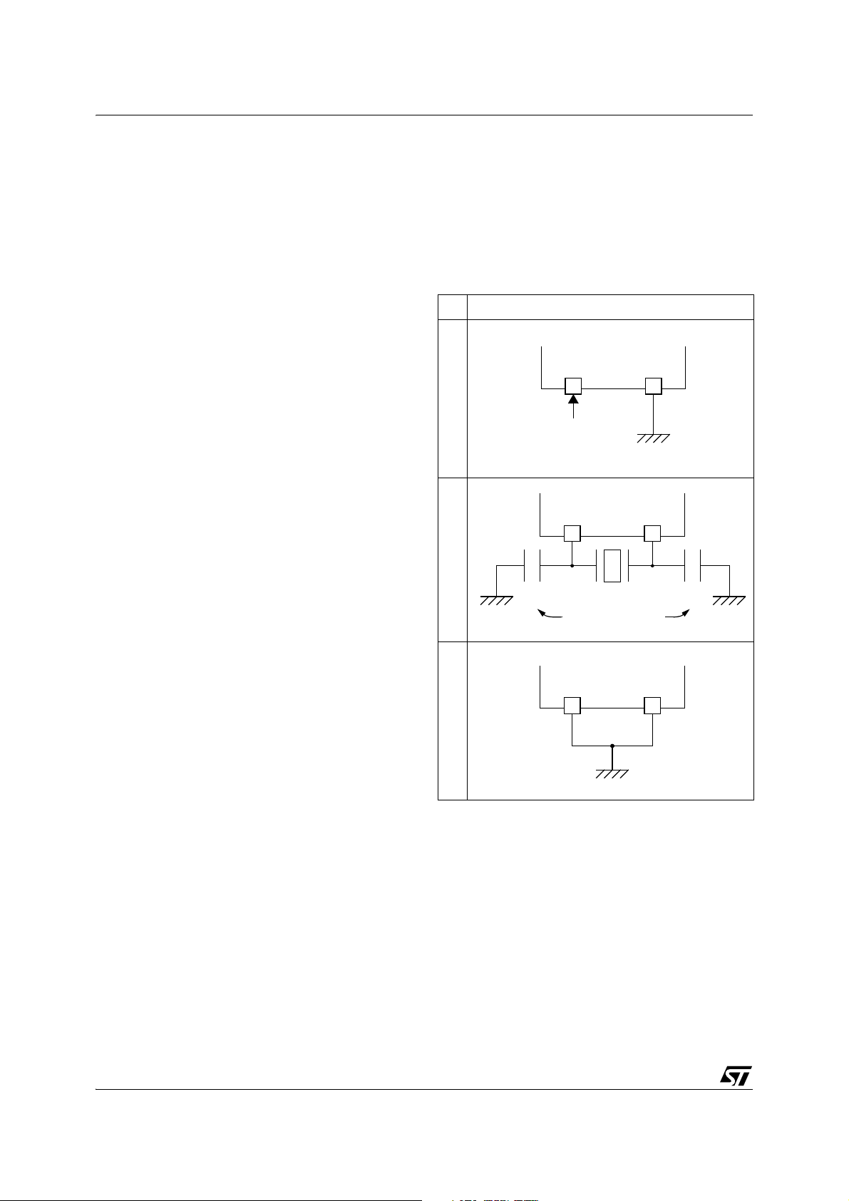
ST72325xx
OSC1 OSC2
EXTERNAL
ST7
SOURCE
OSC1 OSC2
LOAD
CAPACITORS
ST7
C
L2
C
L1
OSC1 OSC2
ST7
6.2 MULTI-OSCILLATOR (MO)
The main clock of the ST7 can be generated by
three different source types coming from the multioscillator block:
■ an external source
■ 4 crystal or ceramic resonator oscillators
■ an internal high frequency RC oscillator
Each oscillator is optimized for a given frequency
range in terms of consumption and is selectable
through the option byte. The associated hardware
configurations are shown in Table 6. Refer to the
electrical characteristics section for more details.
External Clock Source
In this external clock mode, a clock signal (square,
sinus or triangle) with ~50% duty cycle has to drive
the OSC1 pin while the OSC2 pin is tied to ground.
Crystal/Ceramic Oscillators
This family of oscillators has the advantage of producing a very accurate rate on the main clock of
the ST7. The selection within a list of 4 oscillators
with different frequency ranges has to be done by
option byte in order to reduce consumption (refer
to section 14.1 on page 181 for more details on the
frequency ranges). In this mode of the multi-oscillator, the resonator and the load capacitors have
to be placed as close as possible to the oscillator
pins in order to minimize output distortion and
start-up stabilization time. The loading capacitance values must be adjusted according to the
selected oscillator.
These oscillators are not stopped during the
RESET phase to avoid losing time in the oscillator
start-up phase.
Internal RC Oscillator
This oscillator allows a low cost solution for the
main clock of the ST7 using only an internal resistor and capacitor. Internal RC oscillator mode has
the drawback of a lower frequency accuracy and
should not be used in applications that require accurate timing.
In this mode, the two oscillator pins have to be tied
to ground.
Table 6. ST7 Clock Sources
Hardware Configuration
External ClockCrystal/Ceramic ResonatorsInternal RC Oscillator
28/197
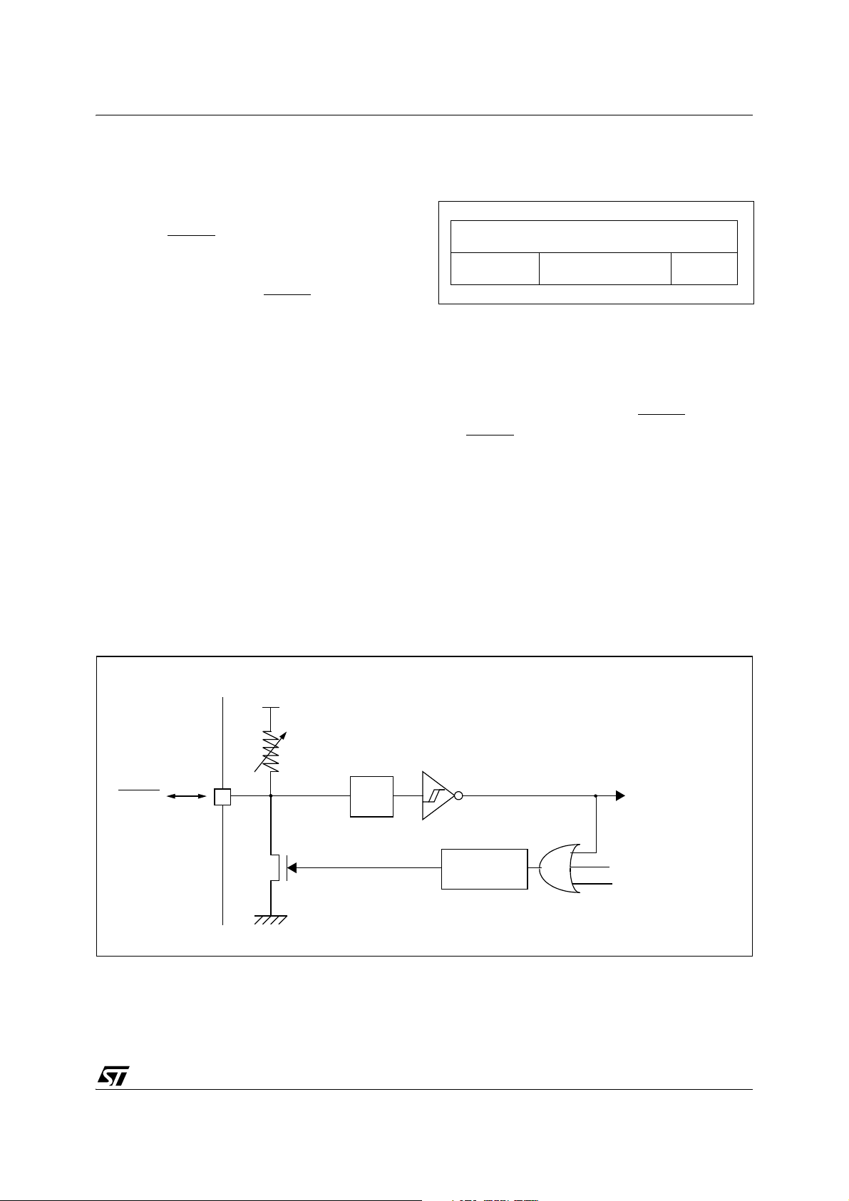
6.3 RESET SEQUENCE MANAGER (RSM)
RESET
Active Phase
INTERNAL RESET
256 or 4096 CLOCK CYCLES
FETCH
VECTOR
RESET
R
ON
V
DD
WATCHDOG RESET
LVD RESET
INTERNAL
RESET
PULSE
GENERATOR
Filter
ST72325xx
6.3.1 Introduction
The reset sequence manager includes three RESET sources as shown in Figure 15:
■ External RESET source pulse
■ Internal LVD RESET (Low Voltage Detection)
■ Internal WATCHDOG RESET
These sources act on the RESET
pin and it is al-
ways kept low during the delay phase.
The RESET service routine vector is fixed at ad-
dresses FFFEh-FFFFh in the ST7 memory map.
The basic RESET sequence consists of 3 phases
as shown in Figure 14:
■ Active Phase depending on the RESET source
■ 256 or 4096 CPU clock cycle delay (selected by
option byte)
■ RESET vector fetch
The 256 or 4096 CPU clock cycle delay allows the
oscillator to stabilise and ensures that recovery
has taken place from the Reset state. The shorter
or longer clock cycle delay should be selected by
option byte to correspond to the stabilization time
of the external oscillator used in the application
(see section 14.1 on page 181).
The RESET vector fetch phase duration is 2 clock
cycles.
Figure 14. RESET Sequence Phases
Caution: When the ST7 is unprogrammed or fully
erased, the Flash is blank and the RESET vector
is not programmed.
For this reason, it is recommended to keep the
RESET pin in low state until programming mode is
entered, in order to avoid unwanted behavior.
6.3.2 Asynchronous External RESET
The RESET
output with integrated R
pin is both an input and an open-drain
weak pull-up resistor.
ON
pin
This pull-up has no fixed value but varies in accordance with the input voltage. It
can be pulled
low by external circuitry to reset the device. See
“CONTROL PIN CHARACTERISTICS” on
page 162 for more details.
A RESET signal originating from an external
source must have a duration of at least t
h(RSTL)in
in
order to be recognized (see Figure 16). This detection is asynchronous and therefore the MCU
can enter reset state even in HALT mode.
Figure 15. Reset Block Diagram
29/197
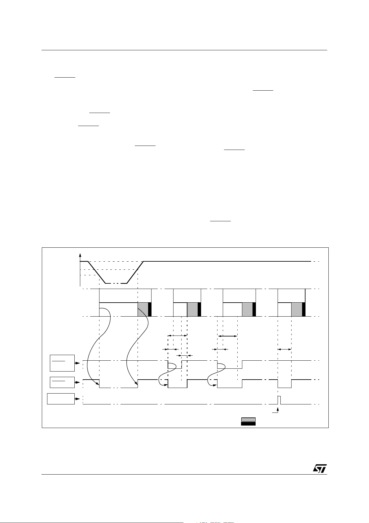
ST72325xx
V
DD
RUN
RESET PIN
EXTERNAL
WATCHDOG
ACTIVE PHASE
V
IT+(LVD)
V
IT-(LVD)
t
h(RSTL)in
t
w(RSTL)out
RUN
t
h(RSTL)in
ACTIVE
WATCHDOG UNDERFLOW
t
w(RSTL)out
RUN RUN RUN
RESET
RESET
SOURCE
SHORT EXT.
RESET
LVD
RESET
LONG EXT.
RESET
WATCHDOG
RESET
INTERNAL RESET (256 or 4096 T
CPU
)
VECTOR FETCH
t
w(RSTL)out
PHASE
ACTIVE
PHASE
ACTIVE
PHASE
DELAY
RESET SEQUENCE MANAGER (Cont’d)
The RESET
plays a major role in EMS performance. In a noisy
environment, it is recommended to follow the
guidelines mentioned in the electrical characteristics section.
If the external RESET
t
w(RSTL)out
signal on the RESET
wise the delay will not be applied (see long ext.
Reset in Figure 16). Starting from the external RESET pulse recognition, the device RESET
as an output that is pulled low during at least
t
w(RSTL)out
6.3.3 External Power-On RESET
If the LVD is disabled by option byte, to start up the
microcontroller correctly, the user must ensure by
means of an external reset circuit that the reset
signal is held low until V
level specified for the selected f
(see “OPERATING CONDITIONS” on page 144)
Figure 16. RESET Sequences
pin is an asynchronous signal which
pulse is shorter than
(see short ext. Reset in Figure 16), the
pin may be stretched. Other-
pin acts
.
is over the minimum
DD
frequency.
OSC
A proper reset signal for a slow rising V
supply
DD
can generally be provided by an external RC network connected to the RESET
pin.
6.3.4 Internal Low Voltage Detector (LVD) RESET
Two different RESET sequences caused by the internal LVD circuitry can be distinguished:
■ Power-On RESET
■ Voltage Drop RESET
The device RESET
pulled low when V
V
DD<VIT-
(falling edge) as shown in Figure 16.
The LVD filters spikes on V
pin acts as an output that is
DD<VIT+
(rising edge) or
larger than t
DD
g(VDD)
to
avoid parasitic resets.
6.3.5 Internal Watchdog RESET
The RESET sequence generated by a internal
Watchdog counter overflow is shown in Figure 16.
Starting from the Watchdog counter underflow, the
device RESET
low during at least t
pin acts as an output that is pulled
w(RSTL)out
.
30/197
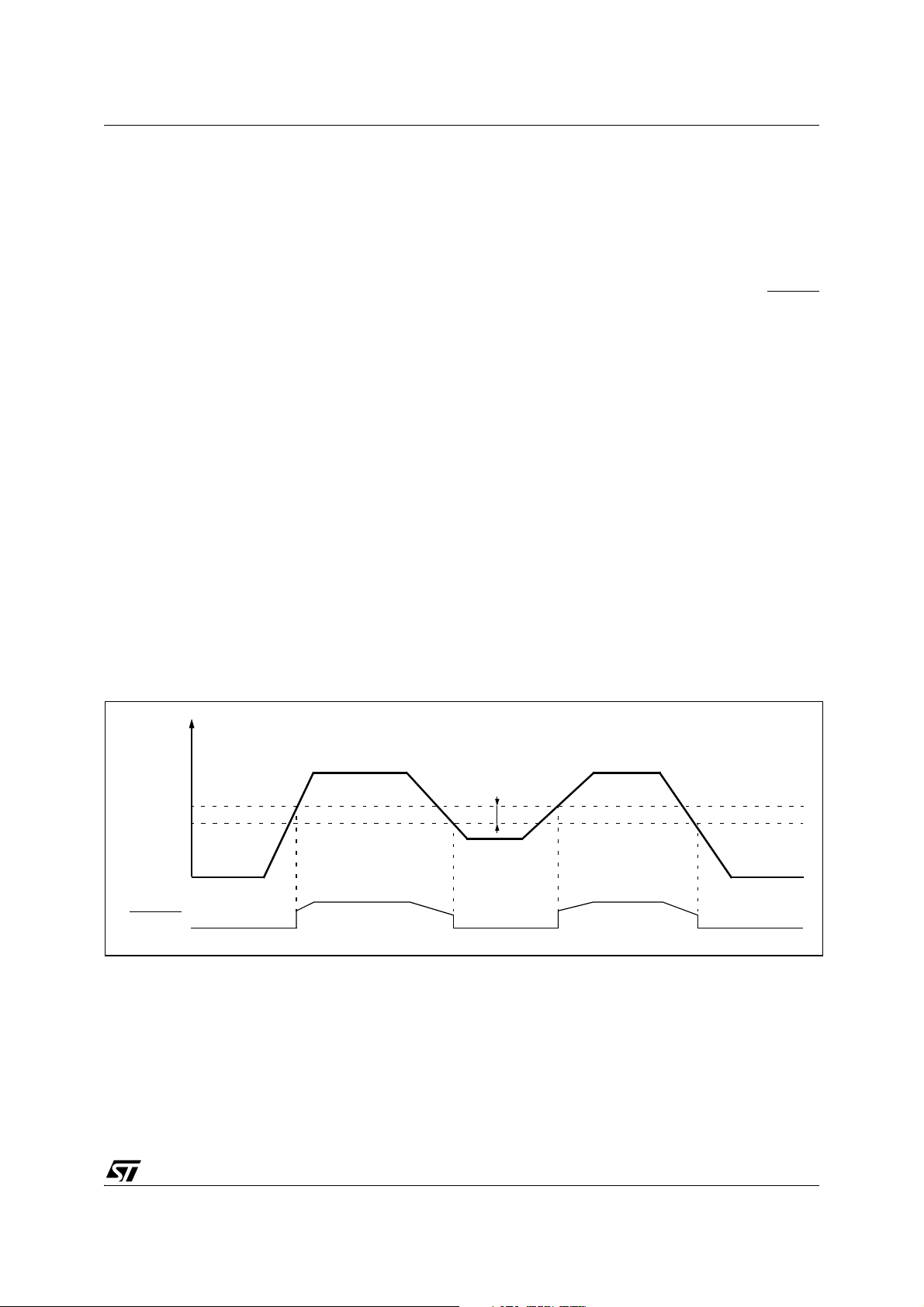
6.4 SYSTEM INTEGRITY MANAGEMENT (SI)
V
DD
V
IT+
RESET
V
IT-
V
hys
ST72325xx
The System Integrity Management block contains
the Low Voltage Detector (LVD) Auxiliary Voltage
Detector (AVD) functions and Clock Security System (CSS). It is managed by the SICSR register.
6.4.1 Low Voltage Detector (LVD)
The Low Voltage Detector function (LVD) generates a static reset when the V
below a V
reference value. This means that it
IT-
supply voltage is
DD
secures the power-up as well as the power-down
keeping the ST7 in reset.
The V
than the V
reference value for a voltage drop is lower
IT-
reference value for power-on in order
IT+
to avoid a parasitic reset when the MCU starts running and sinks current on the supply (hysteresis).
The LVD Reset circuitry generates a reset when
is below:
V
DD
when VDD is rising
–V
IT+
when VDD is falling
–V
IT-
The LVD function is illustrated in Figure 17.
The voltage threshold can be configured by option
byte to be low, medium or high.
Provided the minimum V
the oscillator frequency) is above V
value (guaranteed for
DD
, the MCU
IT-
can only be in two modes:
– under full software control
– in static safe reset
In these conditions, secure operation is always ensured for the application without the need for external reset hardware.
During a Low Voltage Detector Reset, the RESET
pin is held low, thus permitting the MCU to reset
other devices.
Notes:
The LVD allows the device to be used without any
external RESET circuitry.
If the medium or low thresholds are selected, the
detection may occur outside the specified operating voltage range. Below 3.8V, device operation is
not guaranteed.
The LVD is an optional function which can be selected by option byte.
It is recommended to make sure that the V
DD
supply voltage rises monotonously when the device is
exiting from Reset, to ensure the application functions properly.
Figure 17. Low Voltage Detector vs Reset
31/197

ST72325xx
V
DD
V
IT+(AVD)
V
IT-(AVD)
AVDF bit 0 0RESET VALUE
IF AVDIE bit = 1
V
hyst
AVD INTERRUPT
REQUEST
INTERRUPT PROCESS
INTERRUPT PROCESS
V
IT+(LVD)
V
IT-(LVD)
LVD RESET
Early Warning Interrupt
(Power has dropped, MCU not
not yet in reset)
1
1
t
rv
VOLTAGE RISE TIME
SYSTEM INTEGRITY MANAGEMENT (Cont’d)
6.4.2 Auxiliary Voltage Detector (AVD)
The Voltage Detector function (AVD) is based on
an analog comparison between a V
V
IT+(AVD)
reference value and the VDD main sup-
IT-(AVD)
ply or the external EVD pin voltage level (V
The V
than the V
reference value for falling voltage is lower
IT-
reference value for rising voltage in
IT+
order to avoid parasitic detection (hysteresis).
The output of the AVD comparator is directly read-
able by the application software through a real
time status bit (AVDF) in the SICSR register. This
bit is read only.
Caution: The AVD function is active only if the
LVD is enabled through the option byte.
6.4.2.1 Monitoring the V
Main Supply
DD
This mode is selected by clearing the AVDS bit in
the SICSR register.
The AVD voltage threshold value is relative to the
selected LVD threshold configured by option byte
(see section 14.1 on page 181).
If the AVD interrupt is enabled, an interrupt is generated when the voltage crosses the V
V
IT-(AVD)
threshold (AVDF bit toggles).
Figure 18. Using the AVD to Monitor V
and
EVD
IT+(AVD)
(AVDS bit=0)
DD
or
In the case of a drop in voltage, the AVD interrupt
acts as an early warning, allowing software to shut
down safely before the LVD resets the microcontroller. See Figure 18.
).
The interrupt on the rising edge is used to inform
the application that the V
If the voltage rise time t
warning state is over.
DD
is less than 256 or 4096
rv
CPU cycles (depending on the reset delay selected by option byte), no AVD interrupt will be generated when V
is greater than 256 or 4096 cycles then:
If t
rv
IT+(AVD)
is reached.
– If the AVD interrupt is enabled before the
V
IT+(AVD)
threshold is reached, then 2 AVD interrupts will be received: the first when the AVDIE
bit is set, and the second when the threshold is
reached.
– If the AVD interrupt is enabled after the V
threshold is reached then only one AVD interrupt
will occur.
IT+(AVD)
32/197

SYSTEM INTEGRITY MANAGEMENT (Cont’d)
V
EVD
V
IT+(EVD)
V
IT-(EVD)
AVDF 0 01
IF AVDIE = 1
V
hyst
AVD INTERRUPT
REQUEST
INTERRUPT PROCESS
INTERRUPT PROCESS
6.4.2.2 Monitoring a Voltage on the EVD pin
This mode is selected by setting the AVDS bit in
the SICSR register.
The AVD circuitry can generate an interrupt when
the AVDIE bit of the SICSR register is set. This interrupt is generated on the rising and falling edges
of the comparator output. This means it is generated when either one of these two events occur:
–V
–V
rises up to V
EVD
falls down to V
EVD
IT+(EVD)
The EVD function is illustrated in Figure 19.
For more details, refer to the Electrical Character-
istics section.
Figure 19. Using the Voltage Detector to Monitor the EVD pin (AVDS bit=1)
ST72325xx
IT-(EVD)
33/197
ST72325xx
f
OSC2
f
CPU
f
OSC2
f
CPU
f
SFOSC
PLL ON
Clock Filter Function
Clock Detection Function
SYSTEM INTEGRITY MANAGEMENT (Cont’d)
6.4.3 Clock Security System (CSS)
The Clock Security System (CSS) protects the
ST7 against breakdowns, spikes and overfrequencies occurring on the main clock source (f
is based on a clock filter and a clock detection control with an internal safe oscillator (f
SFOSC
6.4.3.1 Clock Filter Control
The PLL has an integrated glitch filtering capability
making it possible to protect the internal clock from
overfrequencies created by individual spikes. This
feature is available only when the PLL is enabled.
If glitches occur on f
(for example, due to loose
OSC
connection or noise), the CSS filters these automatically, so the internal CPU frequency (f
continues deliver a glitch-free signal (see Figure
20).
6.4.3.2 Clock detection Control
If the clock signal disappears (due to a broken or
disconnected resonator...), the safe oscillator delivers a low frequency clock signal (f
SFOSC
allows the ST7 to perform some rescue operations.
Automatically, the ST7 clock source switches back
from the safe oscillator (f
source (f
) recovers.
OSC
When the internal clock (f
oscillator (f
), the application software is noti-
SFOSC
) if the main clock
SFOSC
) is driven by the safe
CPU
fied by hardware setting the CSSD bit in the SICSR register. An interrupt can be generated if the
OSC
).
CPU
) which
). It
CSSIE bit has been previously set.
These two bits are described in the SICSR register
description.
6.4.4 Low Power Modes
Mode Description
WAIT
HALT
)
No effect on SI. CSS and AVD interrupts
cause the device to exit from Wait mode.
The SICSR register is frozen.The CSS (including the safe oscillator) is disabled until
HALT mode is exited. The previous CSS
configuration resumes when the MCU is
woken up by an interrupt with “exit from
HALT mode” capability or from the counter
reset value when the MCU is woken up by a
RESET.
6.4.4.1 Interrupts
The CSS orAVD interrupt events generate an interrupt if the corresponding Enable Control Bit
(CSSIE or AVDIE) is set and the interrupt mask in
the CC register is reset (RIM instruction).
Flag
Enable
Control
Bit
Interrupt Event
CSS event detection
(safe oscillator activated as main clock)
AVD event AVDF AVDIE Yes No
Event
CSSD CSSIE Yes No
Exit
from
Wait
Exit
from
Halt
Figure 20. Clock Filter Function
34/197

SYSTEM INTEGRITY MANAGEMENT (Cont’d)
6.4.5 Register Description SYSTEM INTEGRITY (SI) CONTROL/STATUS REGISTER (SICSR)
Read/Write
Reset Value: 000x 000x (00h)
70
AVD
AVD
S
IE
AVDFLVD
RF
CSSIECSSDWDG
0
RF
is detected by the Clock Security System (CSSD
bit set). It is set and cleared by software.
0: Clock security system interrupt disabled
1: Clock security system interrupt enabled
When the CSS is disabled by OPTION BYTE, the
CSSIE bit has no effect.
Bit 1 = CSSD Clock security system detection
Bit 7 = AVDS Voltage Detection selection
This bit is set and cleared by software. Voltage Detection is available only if the LVD is enabled by
option byte.
0: Voltage detection on V
supply
DD
1: Voltage detection on EVD pin
This bit indicates that the safe oscillator of the
Clock Security System block has been selected by
hardware due to a disturbance on the main clock
signal (f
). It is set by hardware and cleared by
OSC
reading the SICSR register when the original oscil-
lator recovers.
0: Safe oscillator is not active
1: Safe oscillator has been activated
Bit 6 = AVDIE Voltage Detector interrupt enable
This bit is set and cleared by software. It enables
When the CSS is disabled by OPTION BYTE, the
CSSD bit value is forced to 0.
an interrupt to be generated when the AVDF flag
changes (toggles). The pending interrupt information is automatically cleared when software enters
the AVD interrupt routine.
0: AVD interrupt disabled
1: AVD interrupt enabled
Bit 0 = WDGRF Watchdog reset flag
This bit indicates that the last Reset was generat-
ed by the Watchdog peripheral. It is set by hard-
ware (watchdog reset) and cleared by software
(writing zero) or an LVD Reset (to ensure a stable
cleared state of the WDGRF flag when CPU
Bit 5 = AVDF Voltage Detector flag
This read-only bit is set and cleared by hardware.
If the AVDIE bit is set, an interrupt request is gen-
starts).
Combined with the LVDRF flag information, the
flag description is given by the following table.
erated when the AVDF bit changes value. Refer to
Figure 18 and to Section 6.4.2.1 for additional de-
tails.
0: V
1: V
DD
DD
or V
or V
EVD
EVD
over V
under V
IT+(AVD)
IT-(AVD)
threshold
threshold
RESET Sources LVDRF WDGRF
External RESET
Watchdog 0 1
LVD 1 X
pin 0 0
ST72325xx
Bit 4 = LVDRF LVD reset flag
This bit indicates that the last Reset was generated by the LVD block. It is set by hardware (LVD reset) and cleared by software (writing zero). See
WDGRF flag description for more details. When
the LVD is disabled by OPTION BYTE, the LVDRF
bit value is undefined.
Bit 3 = Reserved, must be kept cleared.
Bit 2 = CSSIE Clock security syst
. interrupt enable
This bit enables the interrupt when a disturbance
Application notes
The LVDRF flag is not cleared when another RE-
SET type occurs (external or watchdog), the
LVDRF flag remains set to keep trace of the origi-
nal failure.
In this case, a watchdog reset can be detected by
software while an external reset can not.
CAUTION: When the LVD is not activated with the
associated option byte, the WDGRF flag can not
be used in the application.
35/197

ST72325xx
“IRET”
RESTORE PC, X, A, CC
STACK PC, X, A, CC
LOAD I1:0 FROM INTERRUPT SW REG.
FETCH NEXT
RESET
TRAP
PENDING
INSTRUCTION
I1:0
FROM STACK
LOAD PC FROM INTERRUPT VECTOR
Y
N
Y
N
Y
N
Interrupt has the same or a
lower software priority
THE INTERRUPT
STAYS PENDING
than current one
Interrupt has a higher
software priority
than current one
EXECUTE
INSTRUCTION
INTERRUPT
7 INTERRUPTS
7.1 INTRODUCTION
The ST7 enhanced interrupt management provides the following features:
■ Hardware interrupts
■ Software interrupt (TRAP)
■ Nested or concurrent interrupt management
with flexible interrupt priority and level
management:
– Up to 4 software programmable nesting levels
– Up to 16 interrupt vectors fixed by hardware
– 2 non maskable events: RESET, TRAP
– 1 maskable Top Level event: TLI
This interrupt management is based on:
– Bit 5 and bit 3 of the CPU CC register (I1:0),
– Interrupt software priority registers (ISPRx),
– Fixed interrupt vector addresses located at the
high addresses of the memory map (FFE0h to
FFFFh) sorted by hardware priority order.
This enhanced interrupt controller guarantees full
upward compatibility with the standard (not nested) ST7 interrupt controller.
7.2 MASKING AND PROCESSING FLOW
The interrupt masking is managed by the I1 and I0
bits of the CC register and the ISPRx registers
which give the interrupt software priority level of
each interrupt vector (see Table 7). The process-
ing flow is shown in Figure 21
When an interrupt request has to be serviced:
– Normal processing is suspended at the end of
the current instruction execution.
– The PC, X, A and CC registers are saved onto
the stack.
– I1 and I0 bits of CC register are set according to
the corresponding values in the ISPRx registers
of the serviced interrupt vector.
– The PC is then loaded with the interrupt vector of
the interrupt to service and the first instruction of
the interrupt service routine is fetched (refer to
“Interrupt Mapping” table for vector addresses).
The interrupt service routine should end with the
IRET instruction which causes the contents of the
saved registers to be recovered from the stack.
Note: As a consequence of the IRET instruction,
the I1 and I0 bits will be restored from the stack
and the program in the previous level will resume.
Table 7. Interrupt Software Priority Levels
Interrupt software priority Level I1 I0
Level 0 (main)
Level 1 0 1
Level 2 0 0
Level 3 (= interrupt disable) 1 1
Low
High
10
Figure 21. Interrupt Processing Flowchart
36/197

INTERRUPTS (Cont’d)
PENDING
SOFTWARE
Different
INTERRUPTS
Same
HIGHEST HARDWARE
PRIORITY SERVICED
PRIORITY
HIGHEST SOFTWARE
PRIORITY SERVICED
ST72325xx
Servicing Pending Interrupts
As several interrupts can be pending at the same
time, the interrupt to be taken into account is determined by the following two-step process:
– the highest software priority interrupt is serviced,
– if several interrupts have the same software pri-
ority then the interrupt with the highest hardware
priority is serviced first.
Figure 22 describes this decision process.
Figure 22. Priority Decision Process
When an interrupt request is not serviced immediately, it is latched and then processed when its
software priority combined with the hardware priority becomes the highest one.
Note 1: The hardware priority is exclusive while
the software one is not. This allows the previous
process to succeed with only one interrupt.
Note 2: TLI,RESET and TRAP can be considered
as having the highest software priority in the decision process.
Different Interrupt Vector Sources
Two interrupt source types are managed by the
ST7 interrupt controller: the non-maskable type
(RESET, TRAP) and the maskable type (external
or from internal peripherals).
Non-Maskable Sources
These sources are processed regardless of the
state of the I1 and I0 bits of the CC register (see
Figure 21). After stacking the PC, X, A and CC
registers (except for RESET), the corresponding
vector is loaded in the PC register and the I1 and
I0 bits of the CC are set to disable interrupts (level
3). These sources allow the processor to exit
HALT mode.
■ TRAP (Non Maskable Software Interrupt)
This software interrupt is serviced when the TRAP
instruction is executed. It will be serviced accord-
ing to the flowchart in Figure 21.
Caution: TRAP can be interrupted by a TLI.
■ RESET
The RESET source has the highest priority in the
ST7. This means that the first current routine has
the highest software priority (level 3) and the high-
est hardware priority.
See the RESET chapter for more details.
Maskable Sources
Maskable interrupt vector sources can be serviced
if the corresponding interrupt is enabled and if its
own interrupt software priority (in ISPRx registers)
is higher than the one currently being serviced (I1
and I0 in CC register). If any of these two condi-
tions is false, the interrupt is latched and thus re-
mains pending.
■ TLI (Top Level Hardware Interrupt)
This hardware interrupt occurs when a specific
edge is detected on the dedicated TLI pin. It will be
serviced according to the flowchart in Figure 21 as
a trap.
Caution: A TRAP instruction must not be used in a
TLI service routine.
■ External Interrupts
External interrupts allow the processor to exit from
HALT low power mode. External interrupt sensitiv-
ity is software selectable through the External In-
terrupt Control register (EICR).
External interrupt triggered on edge will be latched
and the interrupt request automatically cleared
upon entering the interrupt service routine.
If several input pins of a group connected to the
same interrupt line are selected simultaneously,
these will be logically ORed.
■ Peripheral Interrupts
Usually the peripheral interrupts cause the MCU to
exit from HALT mode except those mentioned in
the “Interrupt Mapping” table. A peripheral inter-
rupt occurs when a specific flag is set in the pe-
ripheral status registers and if the corresponding
enable bit is set in the peripheral control register.
The general sequence for clearing an interrupt is
based on an access to the status register followed
by a read or write to an associated register.
Note: The clearing sequence resets the internal
latch. A pending interrupt (i.e. waiting for being
serviced) will therefore be lost if the clear se-
quence is executed.
37/197

ST72325xx
MAIN
IT4
IT2
IT1
TRAP
IT1
MAIN
IT0
I1
HARDWARE PRIORITY
SOFTWARE
3
3
3
3
3
3/0
3
11
11
11
11
11
11 / 10
11
RIM
IT2
IT1
IT4
TRAP
IT3
IT0
IT3
I0
10
PRIORITY
LEVEL
USED STACK = 10 BYTES
MAIN
IT2
TRAP
MAIN
IT0
IT2
IT1
IT4
TRAP
IT3
IT0
HARDWARE PRIORITY
3
2
1
3
3
3/0
3
11
00
01
11
11
11
RIM
IT1
IT4
IT4
IT1
IT2
IT3
I1 I0
11 / 10
10
SOFTWARE
PRIORITY
LEVEL
USED STACK = 20 BYTES
INTERRUPTS (Cont’d)
7.3 INTERRUPTS AND LOW POWER MODES
All interrupts allow the processor to exit the WAIT
low power mode. On the contrary, only external
and other specified interrupts allow the processor
to exit from the HALT modes (see column “Exit
from HALT” in “Interrupt Mapping” table). When
several pending interrupts are present while exiting HALT mode, the first one serviced can only be
an interrupt with exit from HALT mode capability
and it is selected through the same decision process shown in Figure 22.
Note: If an interrupt, that is not able to Exit from
HALT mode, is pending with the highest priority
when exiting HALT mode, this interrupt is serviced
after the first one serviced.
Figure 23. Concurrent Interrupt Management
7.4 CONCURRENT & NESTED MANAGEMENT
The following Figure 23 and Figure 24 show two
different interrupt management modes. The first is
called concurrent mode and does not allow an in-
terrupt to be interrupted, unlike the nested mode in
Figure 24. The interrupt hardware priority is given
in this order from the lowest to the highest: MAIN,
IT4, IT3, IT2, IT1, IT0, TLI. The software priority is
given for each interrupt.
Warning: A stack overflow may occur without no-
tifying the software of the failure.
Figure 24. Nested Interrupt Management
38/197

INTERRUPTS (Cont’d)
ST72325xx
7.5 INTERRUPT REGISTER DESCRIPTION
INTERRUPT SOFTWARE PRIORITY REGIS-
TERS (ISPRX)
CPU CC REGISTER INTERRUPT BITS
Read/Write
Reset Value: 111x 1010 (xAh)
70
11I1 H I0 NZC
Bit 5, 3 = I1, I0 Software Interrupt Priority
These two bits indicate the current interrupt soft-
ware priority.
Interrupt Software Priority Level I1 I0
Level 0 (main)
Level 1 0 1
Level 2 0 0
Level 3 (= interrupt disable*) 1 1
Low
High
10
These two bits are set/cleared by hardware when
entering in interrupt. The loaded value is given by
the corresponding bits in the interrupt software priority registers (ISPRx).
They can be also set/cleared by software with the
RIM, SIM, HALT, WFI, IRET and PUSH/POP instructions (see “Interrupt Dedicated Instruction
Set” table).
*Note: TRAP and RESET events can interrupt a
level 3 program.
Read/Write (bit 7:4 of ISPR3 are read only)
Reset Value: 1111 1111 (FFh)
70
ISPR0 I1_3 I0_3 I1_2 I0_2 I1_1 I0_1 I1_0 I0_0
ISPR1 I1_7 I0_7 I1_6 I0_6 I1_5 I0_5 I1_4 I0_4
ISPR2 I1_11 I0_11 I1_10 I0_10 I1_9 I0_9 I1_8 I0_8
ISPR3 1 1 1 1 I1_13 I0_13 I1_12 I0_12
These four registers contain the interrupt software
priority of each interrupt vector.
– Each interrupt vector (except RESET and TRAP)
has corresponding bits in these registers where
its own software priority is stored. This correspondance is shown in the following table.
Vector address ISPRx bits
FFFBh-FFFAh I1_0 and I0_0 bits*
FFF9h-FFF8h I1_1 and I0_1 bits
... ...
FFE1h-FFE0h I1_13 and I0_13 bits
– Each I1_x and I0_x bit value in the ISPRx regis-
ters has the same meaning as the I1 and I0 bits
in the CC register.
– Level 0 can not be written (I1_x=1, I0_x=0). In
this case, the previously stored value is kept. (example: previous=CFh, write=64h, result=44h)
The TLI, RESET, and TRAP vectors have no soft-
ware priorities. When one is serviced, the I1 and I0
bits of the CC register are both set.
*Note: Bits in the ISPRx registers which corre-
spond to the TLI can be read and written but they
are not significant in the interrupt process man-
agement.
Caution: If the I1_x and I0_x bits are modified
while the interrupt x is executed the following be-
haviour has to be considered: If the interrupt x is
still pending (new interrupt or flag not cleared) and
the new software priority is higher than the previ-
ous one, the interrupt x is re-entered. Otherwise,
the software priority stays unchanged up to the
next interrupt request (after the IRET of the inter-
rupt x).
39/197

ST72325xx
INTERRUPTS (Cont’d)
Table 8. Dedicated Interrupt Instruction Set
Instruction New Description Function/Example I1 H I0 N Z C
HALT Entering Halt mode 1 0
IRET Interrupt routine return Pop CC, A, X, PC I1 H I0 N Z C
JRM Jump if I1:0=11 (level 3) I1:0=11 ?
JRNM Jump if I1:0<>11 I1:0<>11 ?
POP CC Pop CC from the Stack Mem => CC I1 H I0 N Z C
RIM Enable interrupt (level 0 set) Load 10 in I1:0 of CC 1 0
SIM Disable interrupt (level 3 set) Load 11 in I1:0 of CC 1 1
TRAP Software trap Software NMI 1 1
WFI Wait for interrupt 1 0
Note: During the execution of an interrupt routine, the HALT, POPCC, RIM, SIM and WFI instructions change the current
software priority up to the next IRET instruction or one of the previously mentioned instructions.
40/197

ST72325xx
INTERRUPTS (Cont’d)
Table 9. Interrupt Mapping
Exit
N°
0 TLI External top level interrupt EICR yes FFFAh-FFFBh
1
2 ei0 External interrupt port A3..0
3 ei1 External interrupt port F2..0 yes FFF4h-FFF5h
4 ei2 External interrupt port B3..0 yes FFF2h-FFF3h
5 ei3 External interrupt port B7..4 yes FFF0h-FFF1h
6 Not used FFEEh-FFEFh
7 SPI SPI peripheral interrupts SPICSR yes
8 TIMER A TIMER A peripheral interrupts TASR no FFEAh-FFEBh
9 TIMER B TIMER B peripheral interrupts TBSR no FFE8h-FFE9h
10 SCI SCI Peripheral interrupts SCISR
11 AVD Auxiliary Voltage detector interrupt SICSR no FFE4h-FFE5h
12 I2C I2C Peripheral interrupts (see periph) no FFE2h-FFE3h
13 PWM ART PWM ART interrupt ARTCSR yes
Source
Block
RESET Reset
TRAP Software interrupt no FFFCh-FFFDh
MCC/RTC/
CSS
Main clock controller time base interrupt
Safe oscillator activation interrupt
Description
Register
Label
N/A
MCCSR-
SICSR
N/A
Priority
Order
Higher
Priority
Lower
Priority
from
HALT/
ACTIVE
HALT
yes FFFEh-FFFFh
yes FFF8h-FFF9h
yes FFF6h-FFF7h
1
no FFE6h-FFE7h
2
Address
Vector
FFECh-FFEDh
FFE0h-FFE1h
Notes:
1. Exit from HALT possible when SPI is in slave mode.
2. Exit from HALT possible when PWM ART is in external clock mode.
7.6 EXTERNAL INTERRUPTS
7.6.1 I/O Port Interrupt Sensitivity
The external interrupt sensitivity is controlled by
the IPA, IPB and ISxx bits of the EICR register
(Figure 25). This control allows to have up to 4 fully
independent external interrupt source sensitivities.
Each external interrupt source can be generated
on four (or five) different events on the pin:
■ Falling edge
■ Rising edge
■ Falling and rising edge
■ Falling edge and low level
■ Rising edge and high level (only for ei0 and ei2)
To guarantee correct functionality, the sensitivity
bits in the EICR register can be modified only
when the I1 and I0 bits of the CC register are both
set to 1 (level 3). This means that interrupts must
be disabled before changing sensitivity.
The pending interrupts are cleared by writing a different value in the ISx[1:0], IPA or IPB bits of the
EICR.
41/197

ST72325xx
IS10 IS11
EICR
SENSITIVITY
CONTROL
PBOR.3
PBDDR.3
IPB BIT
PB3
ei2 INTERRUPT SOURCE
PORT B [3:0] INTERRUPTS
PB3
PB2
PB1
PB0
IS10 IS11
EICR
SENSITIVITY
CONTROL
PBOR.4
PBDDR.4
PB4
ei3 INTERRUPT SOURCE
PORT B4 INTERRUPT
IS20 IS21
EICR
SENSITIVITY
CONTROL
PAOR.3
PADDR.3
IPA BIT
PA3
ei0 INTERRUPT SOURCE
PORT A3 INTERRUPT
IS20 IS21
EICR
SENSITIVITY
CONTROL
PFOR.2
PFDDR.2
PF2
ei1 INTERRUPT SOURCE
PORT F [2:0] INTERRUPTS
PF2
PF1
PF0
INTERRUPTS (Cont’d)
Figure 25. External Interrupt Control bits
42/197

7.7 EXTERNAL INTERRUPT CONTROL REGISTER (EICR)
ST72325xx
Read/Write
Reset Value: 0000 0000 (00h)
70
IS11 IS10 IPB IS21 IS20 IPA TLIS TLIE
Bit 7:6 = IS1[1:0] ei2 and ei3 sensitivity
The interrupt sensitivity, defined using the IS1[1:0]
bits, is applied to the following external interrupts:
- ei0 (port A3)
IS21 IS20
00
0 1 Rising edge only Falling edge only
1 0 Falling edge only Rising edge only
1 1 Rising and falling edge
External Interrupt Sensitivity
IPA bit =0 IPA bit =1
Falling edge &
low level
- ei2 (port B3..0)
IS11 IS10
00
0 1 Rising edge only Falling edge only
1 0 Falling edge only Rising edge only
1 1 Rising and falling edge
External Interrupt Sensitivity
IPB bit =0 IPB bit =1
Falling edge &
low level
Rising edge
& high level
- ei3 (port B4)
IS11 IS10 External Interrupt Sensitivity
0 0 Falling edge & low level
0 1 Rising edge only
1 0 Falling edge only
1 1 Rising and falling edge
- ei1 (port F2..0)
IS21 IS20 External Interrupt Sensitivity
0 0 Falling edge & low level
0 1 Rising edge only
1 0 Falling edge only
1 1 Rising and falling edge
These 2 bits can be written only when I1 and I0 of
the CC register are both set to 1 (level 3).
Bit 2 = IPA Interrupt polarity for port A
This bit is used to invert the sensitivity of the port A
[3:0] external interrupts. It can be set and cleared
by software only when I1 and I0 of the CC register
are both set to 1 (level 3).
0: No sensitivity inversion
These 2 bits can be written only when I1 and I0 of
1: Sensitivity inversion
the CC register are both set to 1 (level 3).
Bit 5 = IPB Interrupt polarity for port B
This bit is used to invert the sensitivity of the port B
[3:0] external interrupts. It can be set and cleared
by software only when I1 and I0 of the CC register
are both set to 1 (level 3).
0: No sensitivity inversion
Bit 1 = TLIS TLI sensitivity
This bit allows to toggle the TLI edge sensitivity. It
can be set and cleared by software only when
TLIE bit is cleared.
0: Falling edge
1: Rising edge
1: Sensitivity inversion
Bit 0 = TLIE TLI enable
Bit 4:3 = IS2[1:0] ei0 and ei1 sensitivity
The interrupt sensitivity, defined using the IS2[1:0]
bits, is applied to the following external interrupts:
This bit allows to enable or disable the TLI capability on the dedicated pin. It is set and cleared by
software.
0: TLI disabled
1: TLI enabled
Note: a parasitic interrupt can be generated when
clearing the TLIE bit.
Rising edge
& high level
43/197

ST72325xx
INTERRUPTS (Cont’d)
Table 10. Nested Interrupts Register Map and Reset Values
Address
(Hex.)
0024h
0025h
0026h
0027h
0028h
Register
Label
ISPR0
Reset Value
ISPR1
Reset Value
ISPR2
Reset Value
ISPR3
Reset Value1111
EICR
Reset Value
76543210
ei1 ei0 MCC + SI TLI
I1_3
1
I1_7
1
I1_11
1
IS11
0
I0_3
1
SPI ei3 ei2
I0_7
1
AVD SCI TIMER B TIMER A
I0_11
1
IS10
0
I1_2
1
I1_6
1
I1_10
1
IPB
0
I0_2
1
I0_6
1
I0_10
1
I1_13
IS21
0
I1_1
1
I1_5
1
I1_9
1
PWMART I2C
1
IS20
0
I0_1
111
I0_5
1
I0_9
1
I0_13
1
IPA
0
I1_4
I1_8
I1_12
TLIS
I0_4
1
1
1
0
1
I0_8
1
I0_12
1
TLIE
0
44/197

8 POWER SAVING MODES
POWER CONSUMPTION
WAIT
SLOW
RUN
ACTIVE HALT
High
Low
SLOW WAIT
HALT
00 01
SMS
CP1:0
f
CPU
NEW SLOW
NORMAL RUN MODE
MCCSR
FREQUENCY
REQUEST
REQUEST
f
OSC2
f
OSC2
/2 f
OSC2
/4 f
OSC2
ST72325xx
8.1 INTRODUCTION
To give a large measure of flexibility to the application in terms of power consumption, four main
power saving modes are implemented in the ST7
(see Figure 26): SLOW, WAIT (SLOW WAIT), ACTIVE HALT and HALT.
After a RESET the normal operating mode is selected by default (RUN mode). This mode drives
the device (CPU and embedded peripherals) by
means of a master clock which is based on the
main oscillator frequency divided or multiplied by 2
).
(f
OSC2
From RUN mode, the different power saving
modes may be selected by setting the relevant
register bits or by calling the specific ST7 software
instruction whose action depends on the oscillator
status.
Figure 26. Power Saving Mode Transitions
8.2 SLOW MODE
This mode has two targets:
– To reduce power consumption by decreasing the
internal clock in the device,
– To adapt the internal clock frequency (f
CPU
) to
the available supply voltage.
SLOW mode is controlled by three bits in the
MCCSR register: the SMS bit which enables or
disables Slow mode and two CPx bits which select
the internal slow frequency (f
In this mode, the master clock frequency (f
CPU
).
OSC2
can be divided by 2, 4, 8 or 16. The CPU and peripherals are clocked at this lower frequency
).
(f
CPU
Note: SLOW-WAIT mode is activated when entering the WAIT mode while the device is already in
SLOW mode.
Figure 27. SLOW Mode Clock Transitions
)
45/197

ST72325xx
WFI INSTRUCTION
RESET
INTERRUPT
Y
N
N
Y
CPU
OSCILLATOR
PERIPHERALS
I[1:0] BITS
ON
ON
10
OFF
FETCH RESET VECTOR
OR SERVICE INTERRUPT
CPU
OSCILLATOR
PERIPHERALS
I[1:0] BITS
ON
OFF
10
ON
CPU
OSCILLATOR
PERIPHERALS
I[1:0] BITS
ON
ON
XX
1)
ON
256 OR 4096 CPU CLOCK
CYCLE DELAY
POWER SAVING MODES (Cont’d)
8.3 WAIT MODE
WAIT mode places the MCU in a low power consumption mode by stopping the CPU.
This power saving mode is selected by calling the
‘WFI’ instruction.
All peripherals remain active. During WAIT mode,
the I[1:0] bits of the CC register are forced to ‘10’,
to enable all interrupts. All other registers and
memory remain unchanged. The MCU remains in
WAIT mode until an interrupt or RESET occurs,
whereupon the Program Counter branches to the
starting address of the interrupt or Reset service
routine.
The MCU will remain in WAIT mode until a Reset
or an Interrupt occurs, causing it to wake up.
Refer to Figure 28.
Figure 28. WAIT Mode Flow-chart
46/197
Note:
1. Before servicing an interrupt, the CC register is
pushed on the stack. The I[1:0] bits of the CC register are set to the current software priority level of
the interrupt routine and recovered when the CC
register is popped.

POWER SAVING MODES (Cont’d)
HALTRUN RUN
256 OR 4096 CPU
CYCLE DELAY
1)
RESET
OR
INTERRUPT
HALT
INSTRUCTION
FETCH
VECTOR
ACTIVE
[MCCSR.OIE=1]
HALT INSTRUCTION
RESET
Y
N
N
Y
CPU
OSCILLATOR
PERIPHERALS
2)
I[1:0] BITS
ON
OFF
10
OFF
FETCH RESET VECTOR
OR SERVICE INTERRUPT
CPU
OSCILLATOR
PERIPHERALS
I[1:0] BITS
ON
OFF
XX
3)
ON
CPU
OSCILLATOR
PERIPHERALS
I[1:0] BITS
ON
ON
XX
3)
ON
256OR4096CPUCLOCK
CYCLE DELAY
(MCCSR.OIE=1)
INTERRUPT
ST72325xx
8.4 ACTIVE-HALT AND HALT MODES
ACTIVE-HALT and HALT modes are the two lowest power consumption modes of the MCU. They
are both entered by executing the ‘HALT’ instruction. The decision to enter either in ACTIVE-HALT
or HALT mode is given by the MCC/RTC interrupt
enable flag (OIE bit in MCCSR register).
MCCSR
OIE bit
8.4.1 ACTIVE-HALT MODE
ACTIVE-HALT mode is the lowest power consumption mode of the MCU with a real time clock
available. It is entered by executing the ‘HALT’ instruction when the OIE bit of the Main Clock Controller Status register (MCCSR) is set (see section
10.2 on page 61 for more details on the MCCSR
register).
The MCU can exit ACTIVE-HALT mode on recep-
tion of an external interrupt, MCC/RTC interrupt or
a RESET. When exiting ACTIVE-HALT mode by
means of an interrupt, no 256 or 4096 CPU cycle
delay occurs. The CPU resumes operation by
servicing the interrupt or by fetching the reset vector which woke it up (see Figure 30).
When entering ACTIVE-HALT mode, the I[1:0] bits
in the CC register are forced to ‘10b’ to enable interrupts. Therefore, if an interrupt is pending, the
MCU wakes up immediately.
In ACTIVE-HALT mode, only the main oscillator
and its associated counter (MCC/RTC) are running to keep a wake-up time base. All other peripherals are not clocked except those which get their
clock supply from another clock generator (such
as external or auxiliary oscillator).
The safeguard against staying locked in ACTIVEHALT mode is provided by the oscillator interrupt.
Note: As soon as the interrupt capability of one of
the oscillators is selected (MCCSR.OIE bit set),
entering ACTIVE-HALT mode while the Watchdog
is active does not generate a RESET.
This means that the device cannot spend more
than a defined delay in this power saving mode.
CAUTION: When exiting ACTIVE-HALT mode following an MCC/RTC interrupt, OIE bit of MCCSR
register must not be cleared before t
Power Saving Mode entered when HALT
instruction is executed
0 HALT mode
1 ACTIVE-HALT mode
DELAY
after
the interrupt occurs (t
= 256 or 4096 t
DELAY
CPU
delay depending on option byte). Otherwise, the ST7
enters HALT mode for the remaining t
DELAY
peri-
od.
Figure 29. ACTIVE-HALT Timing Overview
Figure 30. ACTIVE-HALT Mode Flow-chart
Notes:
1. This delay occurs only if the MCU exits ACTIVEHALT mode by means of a RESET.
2. Peripheral clocked with an external clock source
can still be active.
3. Before servicing an interrupt, the CC register is
pushed on the stack. The I[1:0] bits of the CC register are set to the current software priority level of
the interrupt routine and restored when the CC
register is popped.
47/197

ST72325xx
HALTRUN RUN
256 OR 4096 CPU
CYCLE DELAY
RESET
OR
INTERRUPT
HALT
INSTRUCTION
FETCH
VECTOR
[MCCSR.OIE=0]
HALT INSTRUCTION
RESET
INTERRUPT
3)
Y
N
N
Y
CPU
OSCILLATOR
PERIPHERALS
2)
I[1:0] BITS
OFF
OFF
10
OFF
FETCH RESET VECTOR
OR SERVICE INTERRUPT
CPU
OSCILLATOR
PERIPHERALS
I[1:0] BITS
ON
OFF
XX
4)
ON
CPU
OSCILLATOR
PERIPHERALS
I[1:0] BITS
ON
ON
XX
4)
ON
256 OR 4096 CPU CLOCK
DELAY
WATCHDOG
ENABLE
DISABLE
WDGHALT
1)
0
WATCHDOG
RESET
1
(MCCSR.OIE=0)
CYCLE
POWER SAVING MODES (Cont’d)
8.4.2 HALT MODE
The HALT mode is the lowest power consumption
mode of the MCU. It is entered by executing the
‘HALT’ instruction when the OIE bit of the Main
Clock Controller Status register (MCCSR) is
cleared (see section 10.2 on page 61 for more details on the MCCSR register).
The MCU can exit HALT mode on reception of either a specific interrupt (see Table 9, “Interrupt
Mapping,” on page 41) or a RESET. When exiting
HALT mode by means of a RESET or an interrupt,
the oscillator is immediately turned on and the 256
or 4096 CPU cycle delay is used to stabilize the
oscillator. After the start up delay, the CPU
resumes operation by servicing the interrupt or by
fetching the reset vector which woke it up (see Fig-
ure 32).
When entering HALT mode, the I[1:0] bits in the
CC register are forced to ‘10b’to enable interrupts.
Therefore, if an interrupt is pending, the MCU
wakes up immediately.
In HALT mode, the main oscillator is turned off
causing all internal processing to be stopped, including the operation of the on-chip peripherals.
All peripherals are not clocked except the ones
which get their clock supply from another clock
generator (such as an external or auxiliary oscillator).
The compatibility of Watchdog operation with
HALT mode is configured by the “WDGHALT” option bit of the option byte. The HALT instruction
when executed while the Watchdog system is enabled, can generate a Watchdog RESET (see sec-
tion 14.1 on page 181 for more details).
Figure 31. HALT Timing Overview
Figure 32. HALT Mode Flow-chart
Notes:
1. WDGHALT is an option bit. See option byte section for more details.
2. Peripheral clocked with an external clock source
can still be active.
3. Only some specific interrupts can exit the MCU
from HALT mode (such as external interrupt). Refer to Table 9, “Interrupt Mapping,” on page 41 for
more details.
4. Before servicing an interrupt, the CC register is
pushed on the stack. The I[1:0] bits of the CC register are set to the current software priority level of
the interrupt routine and recovered when the CC
register is popped.
48/197

POWER SAVING MODES (Cont’d)
8.4.2.1 Halt Mode Recommendations
– Make sure that an external event is available to
wake up the microcontroller from Halt mode.
– When using an external interrupt to wake up the
microcontroller, reinitialize the corresponding I/O
as “Input Pull-up with Interrupt” before executing
the HALT instruction. The main reason for this is
that the I/O may be wrongly configured due to external interference or by an unforeseen logical
condition.
– For the same reason, reinitialize the level sensi-
tiveness of each external interrupt as a precautionary measure.
– The opcode for the HALT instruction is 0x8E. To
avoid an unexpected HALT instruction due to a
program counter failure, it is advised to clear all
occurrences of the data value 0x8E from memo-
ST72325xx
ry. For example, avoid defining a constant in
ROM with the value 0x8E.
– As the HALT instruction clears the interrupt mask
in the CC register to allow interrupts, the user
may choose to clear all pending interrupt bits before executing the HALT instruction. This avoids
entering other peripheral interrupt routines after
executing the external interrupt routine corresponding to the wake-up event (reset or external
interrupt).
Related Documentation
AN 980: ST7 Keypad Decoding Techniques, Implementing Wake-Up on Keystroke
AN1014: How to Minimize the ST7 Power Consumption
AN1605: Using an active RC to wakeup the
ST7LITE0 from power saving mode
49/197

ST72325xx
9 I/O PORTS
9.1 INTRODUCTION
The I/O ports offer different functional modes:
– transfer of data through digital inputs and outputs
and for specific pins:
– external interrupt generation
– alternate signal input/output for the on-chip pe-
ripherals.
An I/O port contains up to 8 pins. Each pin can be
programmed independently as digital input (with or
without interrupt generation) or digital output.
9.2 FUNCTIONAL DESCRIPTION
Each port has two main registers:
– Data Register (DR)
– Data Direction Register (DDR)
and one optional register:
– Option Register (OR)
Each I/O pin may be programmed using the corre-
sponding register bits in the DDR and OR registers: Bit X corresponding to pin X of the port. The
same correspondence is used for the DR register.
The following description takes into account the
OR register, (for specific ports which do not provide this register refer to the I/O Port Implementation section). The generic I/O block diagram is
shown in Figure 1
9.2.1 Input Modes
The input configuration is selected by clearing the
corresponding DDR register bit.
In this case, reading the DR register returns the
digital value applied to the external I/O pin.
Different input modes can be selected by software
through the OR register.
Notes:
1. Writing the DR register modifies the latch value
but does not affect the pin status.
2. When switching from input to output mode, the
DR register has to be written first to drive the correct level on the pin as soon as the port is configured as an output.
3. Do not use read/modify/write instructions (BSET
or BRES) to modify the DR register as this might
corrupt the DR content for I/Os configured as input.
External interrupt function
When an I/O is configured as Input with Interrupt,
an event on this I/O can generate an external interrupt request to the CPU.
Each pin can independently generate an interrupt
request. The interrupt sensitivity is independently
programmable using the sensitivity bits in the
EICR register.
Each external interrupt vector is linked to a dedicated group of I/O port pins (see pinout description
and interrupt section). If several input pins are selected simultaneously as interrupt sources, these
are first detected according to the sensitivity bits in
the EICR register and then logically ORed.
The external interrupts are hardware interrupts,
which means that the request latch (not accessible
directly by the application) is automatically cleared
when the corresponding interrupt vector is
fetched. To clear an unwanted pending interrupt
by software, the sensitivity bits in the EICR register
must be modified.
9.2.2 Output Modes
The output configuration is selected by setting the
corresponding DDR register bit. In this case, writing the DR register applies this digital value to the
I/O pin through the latch. Then reading the DR register returns the previously stored value.
Two different output modes can be selected by
software through the OR register: Output push-pull
and open-drain.
DR register value and output pin status:
DR Push-pull Open-drain
0V
1V
SS
DD
Vss
Floating
9.2.3 Alternate Functions
When an on-chip peripheral is configured to use a
pin, the alternate function is automatically selected. This alternate function takes priority over the
standard I/O programming.
When the signal is coming from an on-chip peripheral, the I/O pin is automatically configured in output mode (push-pull or open drain according to the
peripheral).
When the signal is going to an on-chip peripheral,
the I/O pin must be configured in input mode. In
this case, the pin state is also digitally readable by
addressing the DR register.
Note: Input pull-up configuration can cause unexpected value at the input of the alternate peripheral
input. When an on-chip peripheral use a pin as input and output, this pin has to be configured in input floating mode.
50/197

I/O PORTS (Cont’d)
DR
DDR
OR
DATA BUS
PAD
V
DD
ALTERNATE
ENABLE
ALTERNATE
OUTPUT
1
0
OR SEL
DDR SEL
DR SEL
PULL-UP
CONDITION
P-BUFFER
(see table below)
N-BUFFER
PULL-UP
(see table below)
1
0
ANALOG
INPUT
If implemented
ALTERNATE
INPUT
V
DD
DIODES
(see table below)
EXTERNAL
SOURCE (eix)
INTERRUPT
CMOS
SCHMITT
TRIGGER
REGISTER
ACCESS
Figure 33. I/O Port General Block Diagram
ST72325xx
Table 11. I/O Port Mode Options
Input
Output
Configuration Mode Pull-Up P-Buffer
Floating with/without Interrupt Off
Pull-up with/without Interrupt On
Push-pull
Open Drain (logic level) Off
True Open Drain NI NI NI (see note)
Legend: NI - not implemented
Off - implemented not activated
On - implemented and activated
Off
Note: The diode to V
true open drain pads. A local protection between
the pad and V
vice against positive stress.
Diodes
to V
DD
Off
On
is implemented to protect the de-
SS
On
is not implemented in the
DD
to V
On
SS
51/197

ST72325xx
CONDITION
PAD
V
DD
R
PU
EXTERNAL INTERRUPT
DATA B U S
PULL-UP
INTERRUPT
DR REGISTER ACCESS
W
R
SOURCE (eix)
DR
REGISTER
CONDITION
ALTERNATE INPUT
NOT IMPLEMENTED IN
TRUE OPEN DRAIN
I/O PORTS
ANALOG INPUT
PAD
R
PU
DATA B U S
DR
DR REGISTER ACCESS
R/W
V
DD
ALTERNATEALTERNATE
ENABLE OUTPUT
REGISTER
NOT IMPLEMENTED IN
TRUE OPEN DRAIN
I/O PORTS
PAD
R
PU
DATA B U S
DR
DR REGISTER ACCESS
R/W
V
DD
ALTERNATEALTERNATE
ENABLE OUTPUT
REGISTER
NOT IMPLEMENTED IN
TRUE OPEN DRAIN
I/O PORTS
I/O PORTS (Cont’d)
Table 12. I/O Port Configurations
1)
INPUT
Hardware Configuration
2)
2)
Notes:
1. When the I/O port is in input configuration and the associated alternate function is enabled as an output,
2. When the I/O port is in output configuration and the associated alternate function is enabled as an input,
52/197
OPEN-DRAIN OUTPUT
PUSH-PULL OUTPUT
reading the DR register will read the alternate function output status.
the alternate function reads the pin status given by the DR register content.

I/O PORTS (Cont’d)
01
floating/pull-up
interrupt
INPUT
00
floating
(reset state)
INPUT
10
open-drain
OUTPUT
11
push-pull
OUTPUT
XX
= DDR, OR
CAUTION: The alternate function must not be activated as long as the pin is configured as input
with interrupt, in order to avoid generating spurious
interrupts.
Analog alternate function
When the pin is used as an ADC input, the I/O
must be configured as floating input. The analog
multiplexer (controlled by the ADC registers)
switches the analog voltage present on the selected pin to the common analog rail which is connected to the ADC input.
It is recommended not to change the voltage level
or loading on any port pin while conversion is in
progress. Furthermore it is recommended not to
have clocking pins located close to a selected analog pin.
WARNING: The analog input voltage level must
be within the limits stated in the absolute maximum ratings.
9.3 I/O PORT IMPLEMENTATION
The hardware implementation on each I/O port depends on the settings in the DDR and OR registers
and specific feature of the I/O port such as ADC Input or true open drain.
Switching these I/O ports from one state to another should be done in a sequence that prevents unwanted side effects. Recommended safe transitions are illustrated in Figure 2 on page 4. Other
transitions are potentially risky and should be
avoided, since they are likely to present unwanted
side-effects such as spurious interrupt generation.
ST72325xx
Figure 34. Interrupt I/O Port State Transitions
9.4 LOW POWER MODES
Mode Description
WAIT
HALT
9.5 INTERRUPTS
The external interrupt event generates an interrupt
if the corresponding configuration is selected with
DDR and OR registers and the interrupt mask in
the CC register is not active (RIM instruction).
Interrupt Event
External interrupt on
selected external
event
No effect on I/O ports. External interrupts
cause the device to exit from WAIT mode.
No effect on I/O ports. External interrupts
cause the device to exit from HALT mode.
Event
Flag
-
Enable
Control
Bit
DDRx
ORx
Exit
from
Wait
Exit
from
Halt
Yes
53/197

ST72325xx
I/O PORTS (Cont’d)
9.5.1 I/O Port Implementation
The I/O port register configurations are summarised as follows.
Standard Ports
PA5:4, PC7:0, PD7:0, PE7:3,
floating input 0 0
floating interrupt input 0 1
open drain output 1 0
push-pull output 1 1
MODE DDR OR
PE1:0, PF7:3,
MODE DDR OR
floating input 0 0
pull-up input 0 1
open drain output 1 0
push-pull output 1 1
Interrupt Ports
PA2:0, PB6:5, PB4, PB2:0, PF1:0 (with pull-up)
MODE DDR OR
floating input 0 0
pull-up interrupt input 0 1
open drain output 1 0
push-pull output 1 1
True Open Drain Ports
PA7:6
MODE DDR
floating input 0
open drain (high sink ports) 1
Pull-Up Input Port PE2
MODE DDR OR
pull-up input 0 x
open drain output* 1 0
push-pull output* 1 1
Table 13. Port Configuration
Port Pin name
PA7:6 floating true open-drain
Port A
Port B
Port C PC7:0 floating pull-up open drain push-pull
Port D PD7:0 floating pull-up open drain push-pull
Port E
Port F
*Pull-up always activated on PE2.
PA5:4 floating pull-up open drain push-pull
PA3 floating floating interrupt open drain push-pull
PA2:0 floating pull-up interrupt open drain push-pull
PB7, PB3 floating floating interrupt open drain push-pull
PB6:5, PB4,
PB2:0
PE7:3, PE1:0 floating pull-up open drain push-pull
PE2 pull-up input only open drain* push-pull*
PF7:3 floating pull-up open drain push-pull
PF2 floating floating interrupt open drain push-pull
PF1:0 floating pull-up interrupt open drain push-pull
OR = 0 OR = 1 OR = 0 OR = 1
floating pull-up interrupt open drain push-pull
Input Output
54/197

I/O PORTS (Cont’d)
Table 14. I/O Port Register Map and Reset Values
ST72325xx
Address
(Hex.)
Reset Value
of all I/O port registers
0000h PADR
0002h PAOR
0003h PBDR
0005h PBOR
0006h PCDR
0008h PCOR
0009h PDDR
000Bh PDOR
000Ch PEDR
000Eh PEOR
000Fh PFDR
0011h PFOR
Register
Label
76543210
00000000
MSB LSB0001h PADDR
MSB LSB0004h PBDDR
MSB LSB0007h PCDDR
MSB LSB000Ah PDDDR
MSB LSB000Dh PEDDR
MSB LSB0010h PFDDR
Related Documentation
AN 970: SPI Communication between ST7 and
EEPROM
AN1045: S/W implementation of I2C bus master
AN1048: Software LCD driver
55/197

ST72325xx
RESET
WDGA
6-BIT DOWNCOUNTER (CNT)
f
OSC2
T6
T0
WDG PRESCALER
WATCHDOG CONTROL REGISTER (WDGCR)
DIV 4
T1
T2
T3
T4
T5
12-BIT MCC
RTC COUNTER
MSB
LSB
DIV 64
0
5
6
11
MCC/RTC
TB[1:0] bits
(MCCSR
Register)
10 ON-CHIP PERIPHERALS
10.1 WATCHDOG TIMER (WDG)
10.1.1 Introduction
The Watchdog timer is used to detect the occurrence of a software fault, usually generated by external interference or by unforeseen logical conditions, which causes the application program to
abandon its normal sequence. The Watchdog circuit generates an MCU reset on expiry of a programmed time period, unless the program refreshes the counter’s contents before the T6 bit becomes cleared.
10.1.2 Main Features
■ Programmable free-running downcounter
■ Programmable reset
■ Reset (if watchdog activated) when the T6 bit
reaches zero
■ Optional reset on HALT instruction
(configurable by option byte)
■ Hardware Watchdog selectable by option byte
10.1.3 Functional Description
The counter value stored in the Watchdog Control
register (WDGCR bits T[6:0]), is decremented
every 16384 f
cycles (approx.), and the
OSC2
length of the timeout period can be programmed
by the user in 64 increments.
If the watchdog is activated (the WDGA bit is set)
and when the 7-bit timer (bits T[6:0]) rolls over
from 40h to 3Fh (T6 becomes cleared), it initiates
a reset cycle pulling the reset pin low for typically
30µs.
The application program must write in the
WDGCR register at regular intervals during normal
operation to prevent an MCU reset. This downcounter is free-running: it counts down even if the
watchdog is disabled. The value to be stored in the
WDGCR register must be between FFh and C0h:
– The WDGA bit is set (watchdog enabled)
– The T6 bit is set to prevent generating an imme-
diate reset
– The T[5:0] bits contain the number of increments
which represents the time delay before the
watchdog produces a reset (see Figure 2. Ap-
proximate Timeout Duration). The timing varies
between a minimum and a maximum value due
to the unknown status of the prescaler when writing to the WDGCR register (see Figure 3).
Following a reset, the watchdog is disabled. Once
activated it cannot be disabled, except by a reset.
The T6 bit can be used to generate a software reset (the WDGA bit is set and the T6 bit is cleared).
If the watchdog is activated, the HALT instruction
will generate a Reset.
Figure 35. Watchdog Block Diagram
56/197

WATCHDOG TIMER (Cont’d)
CNT Value (hex.)
Watchdog timeout (ms) @ 8 MHz. f
OSC2
3F
00
38
128
1.5 65
30
28
20
18
10
08
503418 82 98 114
10.1.4 How to Program the Watchdog Timeout
Figure 2 shows the linear relationship between the
6-bit value to be loaded in the Watchdog Counter
(CNT) and the resulting timeout duration in milliseconds. This can be used for a quick calculation
without taking the timing variations into account. If
Figure 36. Approximate Timeout Duration
ST72325xx
more precision is needed, use the formulae in Fig-
ure 3.
Caution: When writing to the WDGCR register, always write 1 in the T6 bit to avoid generating an
immediate reset.
57/197
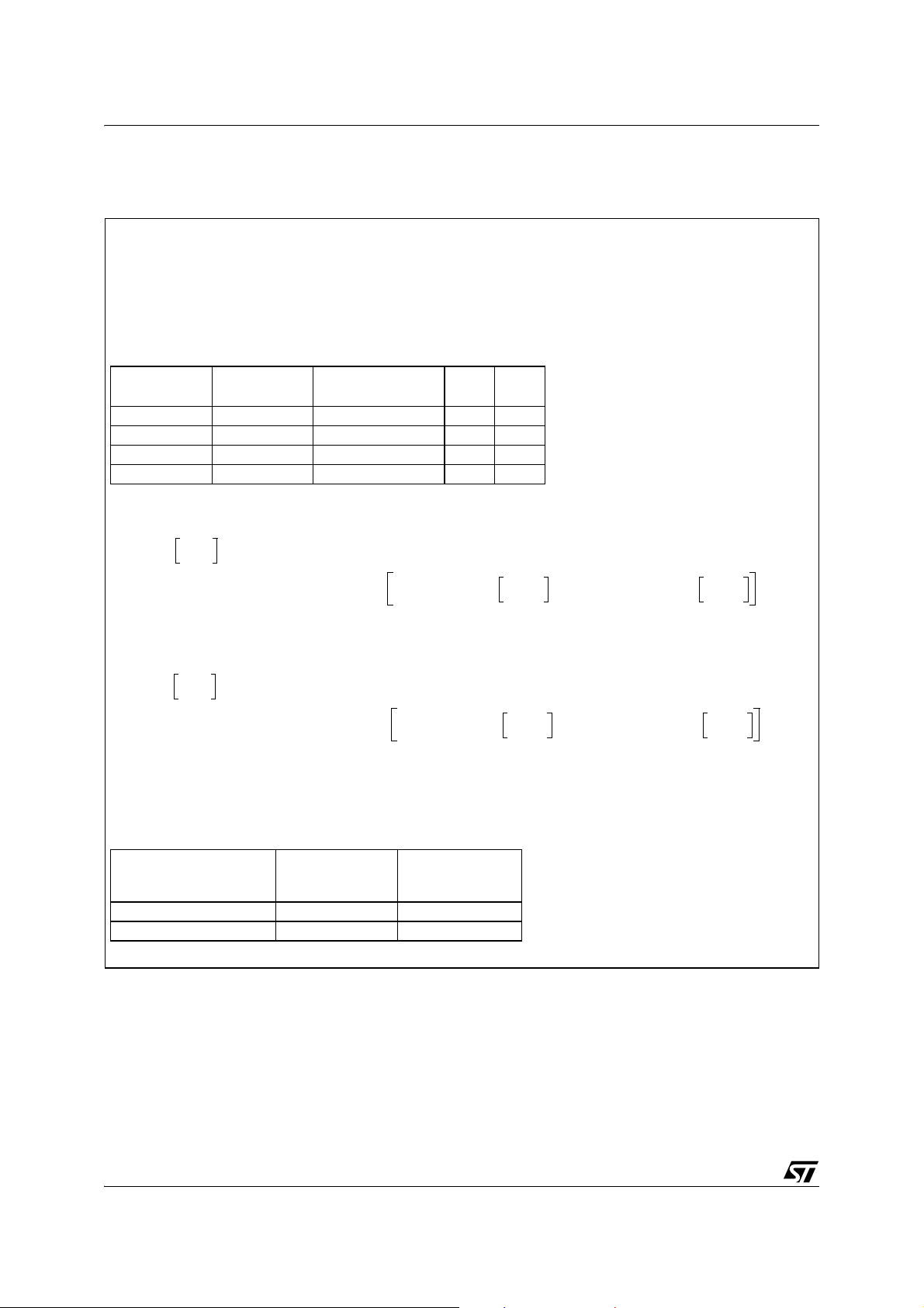
ST72325xx
WHERE:
t
min0
= (LSB + 128) x 64 x t
OSC2
t
max0
= 16384 x t
OSC2
t
OSC2
= 125ns if f
OSC2
=8 MHz
CNT = Value of T[5:0] bits in the WDGCR register (6 bits)
MSB and LSB are values from the table below depending on the timebase selected by the TB[1:0] bits
in the MCCSR register
To calculate the minimum Watchdog Timeout (t
min
):
IF THEN
ELSE
To calculate the maximum Watchdog Timeout (t
max
):
IF THEN
ELSE
Note: In the above formulae, division results must be rounded down to the next integer value.
Example:
With 2ms timeout selected in MCCSR register
TB1 Bit
(MCCSR Reg.)
TB0 Bit
(MCCSR Reg.)
Selected MCCSR
Timebase
MSB LSB
0 0 2ms 4 59
0 1 4ms 8 53
1 0 10ms 20 35
1 1 25ms 49 54
Value of T[5:0] Bits in
WDGCR Register (Hex.)
Min. Watchdog
Timeout (ms)
t
min
Max. Watchdog
Timeout (ms)
t
max
00 1.496 2.048
3F 128 128.552
CNT
MSB
4
-------------
<
t
mintmin0
16384 CNT t
osc2
××+
=
t
mintmin0
16384 CNT
4CNT
MSB
-----------------
–
⎝⎠
⎛⎞
× 192 LSB+()64
4CNT
MSB
-----------------
××
+ t
osc2
×+=
CNT
MSB
4
-------------
≤
t
maxtmax0
16384 CNT t
osc2
××+=
maxtmax0
16384 CNT
4CNT
MSB
-----------------
–
⎝⎠
⎛⎞
× 192 LSB+()64
4CNT
MSB
-----------------
××
+ t
osc2
×+=
WATCHDOG TIMER (Cont’d)
Figure 37. Exact Timeout Duration (t
min
and t
max
)
58/197

WATCHDOG TIMER (Cont’d)
10.1.5 Low Power Modes
Mode Description
SLOW No effect on Watchdog.
WAIT No effect on Watchdog.
OIE bit in
MCCSR
register
00
WDGHALT bit
in Option
Byte
HALT
0 1 A reset is generated.
1x
ST72325xx
No Watchdog reset is generated. The MCU enters Halt mode. The Watchdog counter is decremented once and then stops counting and is no longer
able to generate a watchdog reset until the MCU receives an external interrupt or a reset.
If an external interrupt is received, the Watchdog restarts counting after 256
or 4096 CPU clocks. If a reset is generated, the Watchdog is disabled (reset
state) unless Hardware Watchdog is selected by option byte. For application recommendations see Section 0.1.7 below.
No reset is generated. The MCU enters Active Halt mode. The Watchdog
counter is not decremented. It stop counting. When the MCU receives an
oscillator interrupt or external interrupt, the Watchdog restarts counting immediately. When the MCU receives a reset the Watchdog restarts counting
after 256 or 4096 CPU clocks.
10.1.6 Hardware Watchdog Option
If Hardware Watchdog is selected by option byte,
the watchdog is always active and the WDGA bit in
the WDGCR is not used. Refer to the Option Byte
description.
10.1.7 Using Halt Mode with the WDG (WDGHALT option)
The following recommendation applies if Halt
mode is used when the watchdog is enabled.
– Before executing the HALT instruction, refresh
the WDG counter, to avoid an unexpected WDG
reset immediately after waking up the microcontroller.
10.1.8 Interrupts
None.
10.1.9 Register Description CONTROL REGISTER (WDGCR)
Read/Write
Reset Value: 0111 1111 (7Fh)
70
WDGA T6 T5 T4 T3 T2 T1 T0
Bit 7 = WDGA Activation bit.
This bit is set by software and only cleared by
hardware after a reset. When WDGA = 1, the
watchdog can generate a reset.
0: Watchdog disabled
1: Watchdog enabled
Note: This bit is not used if the hardware watchdog option is enabled by option byte.
Bit 6:0 = T[6:0] 7-bit counter (MSB to LSB).
These bits contain the value of the watchdog
counter. It is decremented every 16384 f
OSC2
cycles (approx.). A reset is produced when it rolls
over from 40h to 3Fh (T6 becomes cleared).
59/197

ST72325xx
Table 15. Watchdog Timer Register Map and Reset Values
Address
(Hex.)
002Ah
Register
Label
WDGCR
Reset Value
76543210
WDGA
0
T6
T5
1
1
T4
1
T3
1
T2
T1
1
1
T0
1
60/197

10.2 MAIN CLOCK CONTROLLER WITH REAL TIME CLOCK AND BEEPER (MCC/RTC)
DIV 2, 4, 8, 16
MCC/RTC INTERRUPT
SMSCP1 CP0 TB1 TB0 OIE OIF
CPU CLOCK
MCCSR
12-BIT MCC RTC
COUNTER
TO CPU AND
PERIPHERALS
f
OSC2
f
CPU
MCO
MCO
BC1 BC0
MCCBCR
BEEP
SELECTION
BEEP SIGNAL
1
0
TO
WATCHDOG
TIMER
DIV 64
ST72325xx
The Main Clock Controller consists of three different functions:
■
a programmable CPU clock prescaler
■
a clock-out signal to supply external devices
■
a real time clock timer with interrupt capability
Each function can be used independently and simultaneously.
10.2.1
Programmable CPU Clock Prescaler
The programmable CPU clock prescaler supplies
the clock for the ST7 CPU and its internal peripherals. It manages SLOW power saving mode (See
Section 8.2 SLOW MODE for more details).
The prescaler selects the f
main clock frequen-
CPU
cy and is controlled by three bits in the MCCSR
register: CP[1:0] and SMS.
10.2.2
Clock-out Capability
The clock-out capability is an alternate function of
an I/O port pin that outputs a f
Figure 38.
Main Clock Controller (MCC/RTC) Block Diagram
clock to drive
CPU
external devices. It is controlled by the MCO bit in
the MCCSR register.
CAUTION: When selected, the clock out pin suspends the clock during ACTIVE-HALT mode.
10.2.3
Real Time Clock Timer (RTC)
The counter of the real time clock timer allows an
interrupt to be generated based on an accurate
real time clock. Four different time bases depending directly on f
are available. The whole
OSC2
functionality is controlled by four bits of the MCCSR register: TB[1:0], OIE and OIF.
When the RTC interrupt is enabled (OIE bit set),
the ST7 enters ACTIVE-HALT mode when the
HALT instruction is executed. See Section 8.4 AC-
TIVE-HALT AND HALT MODES for more details.
10.2.4
Beeper
The beep function is controlled by the MCCBCR
register. It can output three selectable frequencies
on the BEEP pin (I/O port alternate function).
61/197
ST72325xx
MAIN CLOCK CONTROLLER WITH REAL TIME CLOCK (Cont’d)
10.2.5
Low Power Modes
Mode Description
No effect on MCC/RTC peripheral.
WAIT
ACTIVEHALT
HALT
MCC/RTC interrupt cause the device to exit
from WAIT mode.
No effect on MCC/RTC counter (OIE bit is
set), the registers are frozen.
MCC/RTC interrupt cause the device to exit
from ACTIVE-HALT mode.
MCC/RTC counter and registers are frozen.
MCC/RTC operation resumes when the
MCU is woken up by an interrupt with “exit
from HALT” capability.
Bit 6:5 = CP[1:0] CPU clock prescaler
These bits select the CPU clock prescaler which is
applied in the different slow modes. Their action is
conditioned by the setting of the SMS bit. These
two bits are set and cleared by software
f
in SLOW mode CP1 CP0
CPU
f
f
f
f
OSC2
/ 2 0 0
OSC2
/ 4 0 1
OSC2
/ 8 1 0
OSC2
/ 16 1 1
10.2.6
Interrupts
The MCC/RTC interrupt event generates an interrupt if the OIE bit of the MCCSR register is set and
the interrupt mask in the CC register is not active
(RIM instruction).
Interrupt Event
Time base overflow
event
Event
Enable
Control
Flag
OIF OIE Yes No
Bit
Exit
from
Wait
Exit
from
Halt
1)
Note:
The MCC/RTC interrupt wakes up the MCU from
ACTIVE-HALT mode, not from HALT mode.
10.2.7
Register Description
MCC CONTROL/STATUS REGISTER (MCCSR)
Read/Write
Reset Value: 0000 0000 (00h
)
Bit 4 = SMS Slow mode select
This bit is set and cleared by software.
0: Normal mode. f
1: Slow mode. f
= f
CPU
CPU
OSC2
is given by CP1, CP0
See Section 8.2 SLOW MODE and Section 10.2
MAIN CLOCK CONTROLLER WITH REAL TIME
CLOCK AND BEEPER (MCC/RTC) for more de-
tails.
Bit 3:2 = TB[1:0] Time base control
These bits select the programmable divider time
base. They are set and cleared by software.
Counter
Prescaler
16000 4ms 2ms 0 0
32000 8ms 4ms 0 1
80000 20ms 10ms 1 0
200000 50ms 25ms 1 1
f
OSC2
Time Base
=4MHz f
OSC2
A modification of the time base is taken into account at the end of the current period (previously
70
set) to avoid an unwanted time shift. This allows to
use this time base as a real time clock.
MCO CP1 CP0 SMS TB1 TB0 OIE OIF
Bit 7 = MCO Main clock out selection
This bit enables the MCO alternate function on the
PF0 I/O port. It is set and cleared by software.
0: MCO alternate function disabled (I/O pin free for
general-purpose I/O)
1: MCO alternate function enabled (f
CPU
on I/O
port)
Note: To reduce power consumption, the MCO
Bit 1 = OIE Oscillator interrupt enable
This bit set and cleared by software.
0: Oscillator interrupt disabled
1: Oscillator interrupt enabled
This interrupt can be used to exit from ACTIVEHALT mode.
When this bit is set, calling the ST7 software HALT
instruction enters the ACTIVE-HALT power saving
.
mode
function is not active in ACTIVE-HALT mode.
=8MHz
TB1 TB0
62/197

MAIN CLOCK CONTROLLER WITH REAL TIME CLOCK (Cont’d)
Bit 0 = OIF Oscillator interrupt flag
This bit is set by hardware and cleared by software
reading the MCCSR register. It indicates when set
that the main oscillator has reached the selected
elapsed time (TB1:0).
0: Timeout not reached
MCC BEEP CONTROL REGISTER (MCCBCR)
Read/Write
Reset Value: 0000 0000 (00h)
70
1: Timeout reached
CAUTION: The BRES and BSET instructions
must not be used on the MCCSR register to avoid
unintentionally clearing the OIF bit.
000000BC1BC0
Bit 7:2 = Reserved, must be kept cleared.
Bit 1:0 = BC[1:0] Beep control
These 2 bits select the PF1 pin beep capability.
ST72325xx
BC1 BC0 Beep mode with f
00 Off
01 ~2-KHz
10 ~1-KHz
1 1 ~500-Hz
The beep output signal is available in ACTIVEHALT mode but has to be disabled to reduce the
consumption.
Table 16. Main Clock Controller Register Map and Reset Values
Address
(Hex.)
002Bh
002Ch
002Dh
Register
Label
SICSR
Reset Value
MCCSR
Reset Value
MCCBCR
Reset Value000000
76543210
AVDS0AVDIE0AVDF0LVDRF
x0
MCO
0
CP1
0
CP0
0
SMS
0
TB1
0
=8MHz
OSC2
Output
Beep signal
~50% duty cycle
CSSIE0CSSD0WDGRF
x
TB0
0
OIE
0
BC1
0
OIF
0
BC0
0
63/197

ST72325xx
OVF INTERRUPT
EXCL CC2 CC1 CC0 TCE FCRL OIE OVF
ARTCSR
f
INPUT
PWMx
PORT
FUNCTION
ALTERNATE
OCRx
COMPARE
REGISTER
PROGRAMMABLE
PRESCALER
8-BIT COUNTER
(CAR REGISTER)
ARR
REGISTER
ICRx
REGISTER
LOAD
OPx
POLARITY
CONTROL
OEx
PWMCR
MUX
f
CPU
DCRx
REGISTER
LOAD
f
COUNTER
ARTCLK
f
EXT
ARTICx
ICFxICSx
ICCSR
LOAD
ICx INTERRUPT
ICIEx
INPUT CAPTURE
CONTROL
10.3 PWM AUTO-RELOAD TIMER (ART)
10.3.1 Introduction
The Pulse Width Modulated Auto-Reload Timer
on-chip peripheral consists of an 8-bit auto reload
counter with compare/capture capabilities and of a
7-bit prescaler clock source.
These resources allow five possible operating
modes:
– Generation of up to 4 independent PWM signals
– Output compare and Time base interrupt
Figure 39. PWM Auto-Reload Timer Block Diagram
– Up to two input capture functions
– External event detector
– Up to two external interrupt sources
The three first modes can be used together with a
single counter frequency.
The timer can be used to wake up the MCU from
WAIT and HALT modes.
64/197

ON-CHIP PERIPHERALS (Cont’d)
COUNTER
FDh FEh FFh FDh FEh FFh FDh FEh
ARTARR=FDh
f
COUNTER
OCRx
PWMDCRx
FDh
FEh
FDh
FEh
FFh
PWMx
10.3.2 Functional Description
ST72325xx
Counter
The free running 8-bit counter is fed by the output
of the prescaler, and is incremented on every rising edge of the clock signal.
It is possible to read or write the contents of the
counter on the fly by reading or writing the Counter
Access register (ARTCAR).
When a counter overflow occurs, the counter is
automatically reloaded with the contents of the
ARTARR register (the prescaler is not affected).
Counter clock and prescaler
The counter clock frequency is given by:
f
COUNTER
= f
INPUT
The timer counter’s input clock (f
/ 2
CC[2:0]
INPUT
) feeds the
7-bit programmable prescaler, which selects one
of the 8 available taps of the prescaler, as defined
by CC[2:0] bits in the Control/Status Register
(ARTCSR). Thus the division factor of the prescaler can be set to 2
This f
INPUT
n
(where n = 0, 1,..7).
frequency source is selected through
the EXCL bit of the ARTCSR register and can be
either the f
or an external input frequency f
CPU
EXT
The clock input to the counter is enabled by the
TCE (Timer Counter Enable) bit in the ARTCSR
register. When TCE is reset, the counter is
stopped and the prescaler and counter contents
are frozen. When TCE is set, the counter runs at
the rate of the selected clock source.
Counter and Prescaler Initialization
After RESET, the counter and the prescaler are
cleared and f
INPUT
= f
CPU
.
The counter can be initialized by:
– Writing to the ARTARR register and then setting
the FCRL (Force Counter Re-Load) and the TCE
(Timer Counter Enable) bits in the ARTCSR reg-
ister.
– Writing to the ARTCAR counter access register,
In both cases the 7-bit prescaler is also cleared,
whereupon counting will start from a known value.
Direct access to the prescaler is not possible.
Output compare control
The timer compare function is based on four different comparisons with the counter (one for each
PWMx output). Each comparison is made between the counter value and an output compare
register (OCRx) value. This OCRx register can not
be accessed directly, it is loaded from the duty cycle register (PWMDCRx) at each overflow of the
counter.
.
This double buffering method avoids glitch generation when changing the duty cycle on the fly.
Figure 40. Output compare control
65/197

ST72325xx
DUTY CYCLE
REGISTER
AUTO-RELOAD
REGISTER
PWMx OUTPUT
t
255
000
WITH OEx=1
AND OPx=0
(ARTARR)
(PWMDCRx)
WITH OEx=1
AND OPx=1
COUNTER
COUNTER
PWMx OUTPUT
t
WITH OEx=1
AND OPx=0
FDh FEh FFh FDh FEh FFh FDh FEh
OCRx=FCh
OCRx=FDh
OCRx=FEh
OCRx=FFh
ARTARR=FDh
f
COUNTER
ON-CHIP PERIPHERALS (Cont’d)
Independent PWM signal generation
This mode allows up to four Pulse Width Modulated signals to be generated on the PWMx output
pins with minimum core processing overhead.
This function is stopped during HALT mode.
Each PWMx output signal can be selected independently using the corresponding OEx bit in the
PWM Control register (PWMCR). When this bit is
set, the corresponding I/O pin is configured as output push-pull alternate function.
The PWM signals all have the same frequency
which is controlled by the counter period and the
ARTARR register value.
f
PWM
= f
COUNTER
/ (256 - ARTARR)
When a counter overflow occurs, the PWMx pin
level is changed depending on the corresponding
OPx (output polarity) bit in the PWMCR register.
Figure 41. PWM Auto-reload Timer Function
When the counter reaches the value contained in
one of the output compare register (OCRx) the
corresponding PWMx pin level is restored.
It should be noted that the reload values will also
affect the value and the resolution of the duty cycle
of the PWM output signal. To obtain a signal on a
PWMx pin, the contents of the OCRx register must
be greater than the contents of the ARTARR register.
The maximum available resolution for the PWMx
duty cycle is:
Resolution = 1 / (256 - ARTARR)
Note: To get the maximum resolution (1/256), the
ARTARR register must be 0. With this maximum
resolution, 0% and 100% can be obtained by
changing the polarity.
Figure 42. PWM Signal from 0% to 100% Duty Cycle
66/197

ON-CHIP PERIPHERALS (Cont’d)
COUNTER
t
FDh FEh FFh FDh
OVF
ARTCSR READ
INTERRUPT
ARTARR=FDh
f
EXT=fCOUNTER
FEh FFh FDh
IF OIE=1
INTERRUPT
IF OIE=1
ARTCSR READ
ST72325xx
Output compare and Time base interrupt
On overflow, the OVF flag of the ARTCSR register
is set and an overflow interrupt request is generated if the overflow interrupt enable bit, OIE, in the
ARTCSR register, is set. The OVF flag must be reset by the user software. This interrupt can be
External clock and event detector mode
Using the f
auto-reload timer can be used as an external clock
event detector. In this mode, the ARTARR register
is used to select the n
be counted before setting the OVF flag.
used as a time base in the application.
Caution: The external clock function is not available in HALT mode. If HALT mode is used in the application, prior to executing the HALT instruction,
the counter must be disabled by clearing the TCE
bit in the ARTCSR register to avoid spurious counter increments.
Figure 43. External Event Detector Example (3 counts)
external prescaler input clock, the
EXT
number of events to
EVENT
n
= 256 - ARTARR
EVENT
67/197

ST72325xx
04h
COUNTER
t
01h
f
COUNTER
xxh
02h 03h 05h 06h 07h
04h
ARTICx PIN
CFx FLAG
ICRx REGISTER
INTERRUPT
ON-CHIP PERIPHERALS (Cont’d)
Input capture function
This mode allows the measurement of external
signal pulse widths through ARTICRx registers.
Each input capture can generate an interrupt independently on a selected input signal transition.
This event is flagged by a set of the corresponding
CFx bits of the Input Capture Control/Status register (ARTICCSR).
These input capture interrupts are enabled
through the CIEx bits of the ARTICCSR register.
The active transition (falling or rising edge) is software programmable through the CSx bits of the
ARTICCSR register.
The read only input capture registers (ARTICRx)
are used to latch the auto-reload counter value
when a transition is detected on the ARTICx pin
(CFx bit set in ARTICCSR register). After fetching
the interrupt vector, the CFx flags can be read to
identify the interrupt source.
Note: After a capture detection, data transfer in
the ARTICRx register is inhibited until it is read
(clearing the CFx bit).
The timer interrupt remains pending while the CFx
flag is set when the interrupt is enabled (CIEx bit
set). This means, the ARTICRx register has to be
read at each capture event to clear the CFx flag.
External interrupt capability
This mode allows the Input capture capabilities to
be used as external interrupt sources. The interrupts are generated on the edge of the ARTICx
signal.
The edge sensitivity of the external interrupts is
programmable (CSx bit of ARTICCSR register)
and they are independently enabled through CIEx
bits of the ARTICCSR register. After fetching the
interrupt vector, the CFx flags can be read to identify the interrupt source.
During HALT mode, the external interrupts can be
used to wake up the micro (if the CIEx bit is set).
The timing resolution is given by auto-reload counter cycle time (1/f
COUNTER
).
Note: During HALT mode, if both input capture
and external clock are enabled, the ARTICRx register value is not guaranteed if the input capture
pin and the external clock change simultaneously.
Figure 44. Input Capture Timing Diagram
68/197

ON-CHIP PERIPHERALS (Cont’d)
10.3.3 Register Description
ST72325xx
CONTROL / STATUS REGISTER (ARTCSR)
Read/Write
Reset Value: 0000 0000 (00h)
70
0: New transition not yet reached
1: Transition reached
COUNTER ACCESS REGISTER (ARTCAR)
Read/Write
Reset Value: 0000 0000 (00h)
EXCL CC2 CC1 CC0 TCE FCRL OIE OVF
Bit 7 = EXCL
External Clock
70
CA7CA6CA5CA4CA3CA2CA1CA0
This bit is set and cleared by software. It selects the
input clock for the 7-bit prescaler.
0: CPU clock.
1: External clock.
Bit 6:4 = CC[2:0] Counter Clock Control
These bits are set and cleared by software. They
determine the prescaler division ratio from f
f
COUNTER
f
INPUT
f
INPUT
f
INPUT
f
INPUT
f
INPUT
f
INPUT
f
INPUT
f
INPUT
/ 2
/ 4
/ 8
/ 16
/ 32
/ 64
/ 128
With f
=8 MHz CC2 CC1 CC0
INPUT
8 MHz
4 MHz
2 MHz
1 MHz
500 kHz
250 kHz
125 kHz
62.5 kHz
0
0
0
0
1
1
1
1
0
0
1
1
0
0
1
1
INPUT
0
1
0
1
0
1
0
1
Bit 7:0 = CA[7:0] Counter Access Data
These bits can be set and cleared either by hard-
ware or by software. The ARTCAR register is used
to read or write the auto-reload counter “on the fly”
(while it is counting).
.
AUTO-RELOAD REGISTER (ARTARR)
Read/Write
Reset Value: 0000 0000 (00h)
70
AR7AR6AR5AR4AR3AR2AR1AR0
Bit 3 = TCE Timer Counter Enable
This bit is set and cleared by software. It puts the
timer in the lowest power consumption mode.
0: Counter stopped (prescaler and counter frozen).
1: Counter running.
Bit 2 = FCRL
Force Counter Re-Load
This bit is write-only and any attempt to read it will
yield a logical zero. When set, it causes the contents
of ARTARR register to be loaded into the counter,
and the content of the prescaler register to be
cleared in order to initialize the timer before starting
to count.
Bit 1 = OIE
Overflow Interrupt Enable
This bit is set and cleared by software. It allows to
enable/disable the interrupt which is generated
when the OVF bit is set.
0: Overflow Interrupt disable.
1: Overflow Interrupt enable.
Bit 0 = OVF
Overflow Flag
This bit is set by hardware and cleared by software
reading the ARTCSR register. It indicates the transition of the counter from FFh to the ARTARR val-
.
ue
Bit 7:0 =
AR[7:0]
Counter Auto-Reload Data
These bits are set and cleared by software. They
are used to hold the auto-reload value which is automatically loaded in the counter when an overflow
occurs. At the same time, the PWM output levels
are changed according to the corresponding OPx
bit in the PWMCR register.
This register has two PWM management functions:
– Adjusting the PWM frequency
– Setting the PWM duty cycle resolution
PWM Frequency vs Resolution:
f
ARTARR
value
0 8-bit ~0.244 kHz 31.25 kHz
[ 0..127 ] > 7-bit ~0.244 kHz 62.5 kHz
[ 128..191 ] > 6-bit ~0.488 kHz 125 kHz
[ 192..223 ] > 5-bit ~0.977 kHz 250 kHz
[ 224..239 ] > 4-bit ~1.953 kHz 500 kHz
Resolution
PWM
Min Max
69/197

ST72325xx
ON-CHIP PERIPHERALS (Cont’d)
PWM CONTROL REGISTER (PWMCR)
Read/Write
Reset Value: 0000 0000 (00h)
70
OE3 OE2 OE1 OE0 OP3 OP2 OP1 OP0
Bit 7:4 = OE[3:0] PWM Output Enable
These bits are set and cleared by software. They
enable or disable the PWM output channels independently acting on the corresponding I/O pin.
0: PWM output disabled.
1: PWM output enabled.
Bit 3:0 = OP[3:0] PWM Output Polarity
These bits are set and cleared by software. They
independently select the polarity of the four PWM
DUTY CYCLE REGISTERS (PWMDCRx)
Read/Write
Reset Value: 0000 0000 (00h)
70
DC7 DC6 DC5 DC4 DC3 DC2 DC1 DC0
Bit 7:0 = DC[7:0] Duty Cycle Data
These bits are set and cleared by software.
A PWMDCRx register is associated with the OCRx
register of each PWM channel to determine the
second edge location of the PWM signal (the first
edge location is common to all channels and given
by the ARTARR register). These PWMDCR registers allow the duty cycle to be set independently
for each PWM channel.
output signals.
PWMx output level
Counter <= OCRx Counter > OCRx
100
011
OPx
Note: When an OPx bit is modified, the PWMx out-
put signal polarity is immediately reversed.
70/197

ON-CHIP PERIPHERALS (Cont’d)
ST72325xx
INPUT CAPTURE
CONTROL / STATUS REGISTER (ARTICCSR)
Read/Write
INPUT CAPTURE REGISTERS (ARTICRx)
Read only
Reset Value: 0000 0000 (00h)
Reset Value: 0000 0000 (00h)
70
70
IC7 IC6 IC5 IC4 IC3 IC2 IC1 IC0
0 0 CS2 CS1 CIE2 CIE1 CF2 CF1
Bit 7:0 = IC[7:0] Input Capture Data
Bit 7:6 = Reserved, always read as 0.
These read only bits are set and cleared by hard-
ware. An ARTICRx register contains the 8-bit
Bit 5:4 = CS[2:1] Capture Sensitivity
These bits are set and cleared by software. They
auto-reload counter value transferred by the input
capture channel x event.
determine the trigger event polarity on the corresponding input capture channel.
0: Falling edge triggers capture on channel x.
1: Rising edge triggers capture on channel x.
Bit 3:2 = CIE[2:1] Capture Interrupt Enable
These bits are set and cleared by software. They
enable or disable the Input capture channel interrupts independently.
0: Input capture channel x interrupt disabled.
1: Input capture channel x interrupt enabled.
Bit 1:0 = CF[2:1] Capture Flag
These bits are set by hardware and cleared by
software reading the corresponding ARTICRx register. Each CFx bit indicates that an input capture x
has occurred.
0: No input capture on channel x.
1: An input capture has occurred on channel x.
71/197

ST72325xx
PWM AUTO-RELOAD TIMER (Cont’d)
Table 17. PWM Auto-Reload Timer Register Map and Reset Values
Address
(Hex.)
0073h
0074h
0075h
0076h
0077h
0078h
0079h
007Ah
007Bh
007Ch
007Dh
Register
Label
PWMDCR3
Reset Value
PWMDCR2
Reset Value
PWMDCR1
Reset Value
PWMDCR0
Reset Value
PWMCR
Reset Value
ARTCSR
Reset Value
ARTCAR
Reset Value
ARTARR
Reset Value
ARTICCSR
Reset Value
ARTICR1
Reset Value
ARTICR2
Reset Value
76543210
DC7
0
DC7
0
DC7
0
DC7
0
OE3
0
EXCL
0
CA7
0
AR7
0
00
IC7
0
IC7
0
DC6
0
DC6
0
DC6
0
DC6
0
OE2
0
CC2
0
CA6
0
AR6
0
IC6
0
IC6
0
DC5
0
DC5
0
DC5
0
DC5
0
OE1
0
CC1
0
CA5
0
AR5
0
CS2
0
IC5
0
IC5
0
DC4
0
DC4
0
DC4
0
DC4
0
OE0
0
CC0
0
CA4
0
AR4
0
CS1
0
IC4
0
IC4
0
DC3
0
DC3
0
DC3
0
DC3
0
OP3
0
TCE
0
CA3
0
AR3
0
CIE2
0
IC3
0
IC3
0
DC2
0
DC2
0
DC2
0
DC2
0
OP2
0
FCRL
0
CA2
0
AR2
0
CIE1
0
IC2
0
IC2
0
DC1
0
DC1
0
DC1
0
DC1
0
OP1
0
RIE
0
CA1
0
AR1
0
CF2
0
IC1
0
IC1
0
DC0
0
DC0
0
DC0
0
DC0
0
OP0
0
OVF
0
CA0
0
AR0
0
CF1
0
IC0
0
IC0
0
72/197

10.4 16-BIT TIMER
ST72325xx
10.4.1 Introduction
The timer consists of a 16-bit free-running counter
driven by a programmable prescaler.
It may be used for a variety of purposes, including
pulse length measurement of up to two input signals (input capture) or generation of up to two output waveforms (output compare and PWM).
Pulse lengths and waveform periods can be modulated from a few microseconds to several milliseconds using the timer prescaler and the CPU
clock prescaler.
Some ST7 devices have two on-chip 16-bit timers.
They are completely independent, and do not
share any resources. They are synchronized after
a MCU reset as long as the timer clock frequencies are not modified.
This description covers one or two 16-bit timers. In
ST7 devices with two timers, register names are
prefixed with TA (Timer A) or TB (Timer B).
10.4.2 Main Features
■ Programmable prescaler: f
■ Overflow status flag and maskable interrupt
■ External clock input (must be at least four times
slower than the CPU
clock speed) with the choice
divided by 2, 4 or 8
CPU
of active edge
■ 1 or 2 Output Compare functions each with:
– 2 dedicated 16-bit registers
– 2 dedicated programmable signals
– 2 dedicated status flags
– 1 dedicated maskable interrupt
■ 1 or 2 Input Capture functions each with:
– 2 dedicated 16-bit registers
– 2 dedicated active edge selection signals
– 2 dedicated status flags
– 1 dedicated maskable interrupt
■ Pulse width modulation mode (PWM)
■ One Pulse mode
■ Reduced Power Mode
■ 5 alternate functions on I/O ports (ICAP1, ICAP2,
OCMP1, OCMP2, EXTCLK)*
When reading an input signal on a non-bonded
pin, the value will always be ‘1’.
10.4.3 Functional Description
10.4.3.1 Counter
The main block of the Programmable Timer is a
16-bit free running upcounter and its associated
16-bit registers. The 16-bit registers are made up
of two 8-bit registers called high and low.
Counter Register (CR):
– Counter High Register (CHR) is the most sig-
nificant byte (MS Byte).
– Counter Low Register (CLR) is the least sig-
nificant byte (LS Byte).
Alternate Counter Register (ACR)
– Alternate Counter High Register (ACHR) is the
most significant byte (MS Byte).
– Alternate Counter Low Register (ACLR) is the
least significant byte (LS
Byte).
These two read-only 16-bit registers contain the
same value but with the difference that reading the
ACLR register does not clear the TOF bit (Timer
overflow flag), located in the Status register, (SR),
(see note at the end of paragraph titled 16-bit read
sequence).
Writing in the CLR register or ACLR register resets
the free running counter to the FFFCh value.
Both counters have a reset value of FFFCh (this is
the only value which is reloaded in the 16-bit tim-
er). The reset value of both counters is also
FFFCh in One Pulse mode and PWM mode.
The timer clock depends on the clock control bits
of the CR2 register, as illustrated in Table 1. The
value in the counter register repeats every
131072, 262144 or 524288 CPU clock cycles de-
pending on the CC[1:0] bits.
The timer frequency can be f
CPU
/2, f
CPU
/4, f
CPU
/8
or an external frequency.
The Block Diagram is shown in Figure 1.
*Note: Some timer pins may not be available (not
bonded) in some ST7 devices. Refer to the device
pin out description.
73/197
ST72325xx
MCU-PERIPHERAL INTERFACE
COUNTER
ALTERNATE
OUTPUT
COMPARE
REGISTER
OUTPUT COMPARE
EDGE DETECT
OVERFLOW
DETECT
CIRCUIT
1/2
1/4
1/8
8-bit
buffer
ST7 INTERNAL BUS
LATCH1
OCMP1
ICAP1
EXTCLK
f
CPU
TIMER INTERRUPT
ICF2ICF1
TIMD
0
0
OCF2OCF1 TOF
PWMOC1E
EXEDG
IEDG2CC0CC1
OC2E
OPMFOLV2ICIE OLVL1IEDG1OLVL2FOLV1OCIE TOIE
ICAP2
LATCH2
OCMP2
8
8
8 low
16
8 high
16 16
16
16
(Control Register 1) CR1
(Control Register 2) CR2
(Control/Status Register)
6
16
8 8 8
88 8
high
low
high
high
high
low
low
low
EXEDG
TIMER INTERNAL BUS
CIRCUIT1
EDGE DETECT
CIRCUIT2
CIRCUIT
1
OUTPUT
COMPARE
REGISTER
2
INPUT
CAPTURE
REGISTER
1
INPUT
CAPTURE
REGISTER
2
CC[1:0]
COUNTER
pin
pin
pin
pin
pin
REGISTER
REGISTER
Note: If IC, OC and TO interrupt requests have separate vectors
then the last OR is not present (See device Interrupt Vector Table)
(See note)
CSR
16-BIT TIMER (Cont’d)
Figure 45. Timer Block Diagram
74/197

16-BIT TIMER (Cont’d)
is buffered
Read
At t0
Read
Returns the buffered
LS Byte value at t0
At t0 +Δt
Other
instructions
Beginning of the sequence
Sequence completed
LS Byte
LS Byte
MS Byte
16-bit read sequence: (from either the Counter
Register or the Alternate Counter Register).
The user must read the MS Byte first, then the LS
Byte value is buffered automatically.
This buffered value remains unchanged until the
16-bit read sequence is completed, even if the
user reads the MS Byte several times.
After a complete reading sequence, if only the
CLR register or ACLR register are read, they return the LS Byte of the count value at the time of
the read.
Whatever the timer mode used (input capture, output compare, One Pulse mode or PWM mode) an
overflow occurs when the counter rolls over from
FFFFh to 0000h then:
– The TOF bit of the SR register is set.
– A timer interrupt is generated if:
– TOIE bit of the CR1 register is set and
– I bit of the CC register is cleared.
If one of these conditions is false, the interrupt remains pending to be issued as soon as they are
both true.
ST72325xx
Clearing the overflow interrupt request is done in
two steps:
1. Reading the SR register while the TOF bit is set.
2. An access (read or write) to the CLR register.
Notes: The TOF bit is not cleared by accesses to
ACLR register. The advantage of accessing the
ACLR register rather than the CLR register is that
it allows simultaneous use of the overflow function
and reading the free running counter at random
times (for example, to measure elapsed time) without the risk of clearing the TOF bit erroneously.
The timer is not affected by WAIT mode.
In HALT mode, the counter stops counting until the
mode is exited. Counting then resumes from the
previous count (MCU awakened by an interrupt) or
from the reset count (MCU awakened by a Reset).
10.4.3.2 External Clock
The external clock (where available) is selected if
CC0 = 1 and CC1 = 1 in the CR2 register.
The status of the EXEDG bit in the CR2 register
determines the type of level transition on the external clock pin EXTCLK that will trigger the free running counter.
The counter is synchronized with the falling edge
of the internal CPU clock.
A minimum of four falling edges of the CPU clock
must occur between two consecutive active edges
of the external clock; thus the external clock frequency must be less than a quarter of the CPU
clock frequency.
75/197

ST72325xx
CPU CLOCK
FFFD
FFFE FFFF 0000 0001 0002 0003
INTERNAL RESET
TIMER CLOCK
COUNTER REGISTER
TIMER OVERFLOW FLAG (TOF)
FFFC FFFD 0000 0001
CPU CLOCK
INTERNAL RESET
TIMER CLOCK
COUNTER REGISTER
TIMER OVERFLOW FLAG (TOF)
CPU CLOCK
INTERNAL RESET
TIMER CLOCK
COUNTER REGISTER
TIMER OVERFLOW FLAG (TOF)
FFFC FFFD
0000
16-BIT TIMER (Cont’d)
Figure 46. Counter Timing Diagram, Internal Clock Divided by 2
Figure 47. Counter Timing Diagram, Internal Clock Divided by 4
Figure 48. Counter Timing Diagram, Internal Clock Divided By 8
Note: The MCU is in reset state when the internal reset signal is high, when it is low the MCU is running.
76/197

16-BIT TIMER (Cont’d)
10.4.3.3 Input Capture
In this section, the index, i, may be 1 or 2 because
there are two input capture functions in the 16-bit
timer.
The two 16-bit input capture registers (IC1R and
IC2R) are used to latch the value of the free running counter after a transition is detected on the
ICAPi pin (see Figure 5).
MS Byte LS Byte
ICiR ICiHR ICiLR
ICiR register is a read-only register.
The active transition is software programmable
through the IEDGi bit of Control Registers (CRi).
Timing resolution is one count of the free running
f
counter: (
CPU
/CC[1:0]).
Procedure:
To use the input capture function select the following in the CR2 register:
– Select the timer clock (CC[1:0]) (see Table 1).
– Select the edge of the active transition on the
ICAP2 pin with the IEDG2 bit (the ICAP2 pin
must be configured as floating input or input with
pull-up without interrupt if this configuration is
available).
And select the following in the CR1 register:
– Set the ICIE bit to generate an interrupt after an
input capture coming from either the ICAP1 pin
or the ICAP2 pin
– Select the edge of the active transition on the
ICAP1 pin with the IEDG1 bit (the ICAP1pin must
be configured as floating input or input with pull-
up without interrupt if this configuration is availa-
ble).
ST72325xx
When an input capture occurs:
– ICFi bit is set.
– The ICiR register contains the value of the free
running counter on the active transition on the
ICAPi pin (see Figure 6).
– A timer interrupt is generated if the ICIE bit is set
and the I bit is cleared in the CC register. Otherwise, the interrupt remains pending until both
conditions become true.
Clearing the Input Capture interrupt request (that
is, clearing the ICFi bit) is done in two steps:
1. Reading the SR register while the ICFi bit is set.
2. An access (read or write) to the ICiLR register.
Notes:
1. After reading the ICiHR register, transfer of
input capture data is inhibited and ICFi will
never be set until the ICiLR register is also
read.
2. The ICiR register contains the free running
counter value which corresponds to the most
recent input capture.
3. The two input capture functions can be used
together even if the timer also uses the two output compare functions.
4. In One Pulse mode and PWM mode only Input
Capture 2 can be used.
5. The alternate inputs (ICAP1 and ICAP2) are
always directly connected to the timer. So any
transitions on these pins activates the input
capture function.
Moreover if one of the ICAPi pins is configured
as an input and the second one as an output,
an interrupt can be generated if the user toggles the output pin and if the ICIE bit is set.
This can be avoided if the input capture function i is disabled by reading the ICiHR (see note
1).
6. The TOF bit can be used with interrupt generation in order to measure events that go beyond
the timer range (FFFFh).
77/197
ST72325xx
ICIE
CC0
CC1
16-BIT FREE RUNNING
COUNTER
IEDG1
(Control Register 1) CR1
(Control Register 2) CR2
ICF2ICF1 000
(Status Register) SR
IEDG2
ICAP1
ICAP2
EDGE DETECT
CIRCUIT2
16-BIT
IC1R Register
IC2R Register
EDGE DETECT
CIRCUIT1
pin
pin
FF01 FF02 FF03
FF03
TIMER CLOCK
COUNTER REGISTER
ICAPi PIN
ICAPi FLAG
ICAPi REGISTER
Note: The rising edge is the active edge.
16-BIT TIMER (Cont’d)
Figure 49. Input Capture Block Diagram
Figure 50. Input Capture Timing Diagram
78/197

16-BIT TIMER (Cont’d)
Δ OCiR =
Δt * f
CPU
PRESC
Δ OCiR = Δt
* fEXT
10.4.3.4 Output Compare
In this section, the index, i, may be 1 or 2 because
there are two output compare functions in the 16bit timer.
This function can be used to control an output
waveform or indicate when a period of time has
elapsed.
When a match is found between the Output Compare register and the free running counter, the output compare function:
– Assigns pins with a programmable value if the
OCiE bit is set
– Sets a flag in the status register
– Generates an interrupt if enabled
Two 16-bit registers Output Compare Register 1
(OC1R) and Output Compare Register 2 (OC2R)
contain the value to be compared to the counter
register each timer clock cycle.
MS Byte LS Byte
OCiROCiHR OCiLR
These registers are readable and writable and are
not affected by the timer hardware. A reset event
changes the OC
iR value to 8000h.
Timing resolution is one count of the free running
counter: (
f
CPU/
CC[1:0]
).
Procedure:
To use the output compare function, select the following in the CR2 register:
– Set the OCiE bit if an output is needed then the
OCMPi pin is dedicated to the output compare i
signal.
– Select the timer clock (CC[1:0]) (see Table 1).
And select the following in the CR1 register:
– Select the OLVLi bit to applied to the OCMPi pins
after the match occurs.
– Set the OCIE bit to generate an interrupt if it is
needed.
When a match is found between OCiR register
and CR register:
– OCFi bit is set.
ST72325xx
– The OCMPi pin takes OLVLi bit value (OCMPi
pin latch is forced low during reset).
– A timer interrupt is generated if the OCIE bit is
set in the CR1 register and the I bit is cleared in
the CC register (CC).
The OC
iR register value required for a specific tim-
ing application can be calculated using the following formula:
Where:
Δt = Output compare period (in seconds)
f
= CPU clock frequency (in hertz)
CPU
PRESC
= Timer prescaler factor (2, 4 or 8 de-
pending on CC[1:0] bits, see Table 1)
If the timer clock is an external clock, the formula
is:
Where:
Δt = Output compare period (in seconds)
f
= External timer clock frequency (in hertz)
EXT
Clearing the output compare interrupt request
(that is, clearing the OCFi bit) is done by:
1. Reading the SR register while the OCFi bit is
set.
2. An access (read or write) to the OCiLR register.
The following procedure is recommended to prevent the OCFi bit from being set between the time
it is read and the write to the OC
– Write to the OCiHR register (further compares
are inhibited).
– Read the SR register (first step of the clearance
of the OCFi bit, which may be already set).
– Write to the OCiLR register (enables the output
compare function and clears the OCFi bit).
iR register:
79/197

ST72325xx
OUTPUT COMPARE
16-bit
CIRCUIT
OC1R Register
16 BIT FREE RUNNING
COUNTER
OC1E CC0CC1
OC2E
OLVL1OLVL2OCIE
(Control Register 1) CR1
(Control Register 2) CR2
000OCF2OCF1
(Status Register) SR
16-bit
16-bit
OCMP1
OCMP2
Latch
1
Latch
2
OC2R Register
Pin
Pin
FOLV2 FOLV1
16-BIT TIMER (Cont’d)
Notes:
1. After a processor write cycle to the OCiHR reg-
ister, the output compare function is inhibited
until the OCiLR register is also written.
2. If the OCiE bit is not set, the OCMPi pin is a
general I/O port and the OLVLi bit will not
appear when a match is found but an interrupt
could be generated if the OCIE bit is set.
3. In both internal and external clock modes,
OCFi and OCMPi are set while the counter
value equals the OCiR register value (see Fig-
ure 8 for an example with f
for an example with f
CPU
the same in OPM or PWM mode.
4. The output compare functions can be used both
for generating external events on the OCMPi
pins even if the input capture mode is also
used.
5. The value in the 16-bit OC
OLVi bit should be changed after each successful comparison in order to control an output
waveform or establish a new elapsed timeout.
/2 and Figure 9
CPU
/4). This behavior is
iR register and the
Forced Compare Output capability
When the FOLVi bit is set by software, the OLVLi
bit is copied to the OCMPi pin. The OLVi bit has to
be toggled in order to toggle the OCMPi pin when
it is enabled (OCiE bit = 1). The OCFi bit is then
not set by hardware, and thus no interrupt request
is generated.
The FOLVLi bits have no effect in both One Pulse
mode and PWM mode.
Figure 51. Output Compare Block Diagram
80/197

16-BIT TIMER (Cont’d)
INTERNAL CPU CLOCK
TIMER CLOCK
COUNTER REGISTER
OUTPUT COMPARE REGISTER i (OCRi)
OUTPUT COMPARE FLAG i (OCFi)
OCMPi PIN (OLVLi =1)
2ED3
2ED0 2ED1 2ED2
2ED3
2ED42ECF
INTERNAL CPU CLOCK
TIMER CLOCK
COUNTER REGISTER
OUTPUT COMPARE REGISTER i (OCRi)
2ED3
2ED0 2ED1 2ED2
2ED3
2ED42ECF
OUTPUT COMPARE FLAG i (OCFi)
OCMPi PIN (OLVLi =1)
ST72325xx
Figure 52. Output Compare Timing Diagram, f
Figure 53. Output Compare Timing Diagram, f
TIMER
TIMER
=f
=f
CPU
CPU
/2
/4
81/197

ST72325xx
event occurs
Counter
= OC1R
OCMP1 = OLVL1
When
When
on ICAP1
One Pulse mode cycle
OCMP1 = OLVL2
Counter is reset
to FFFCh
ICF1 bit is set
ICR1 = Counter
OCiR Value =
t
*
f
CPU
PRESC
- 5
OCiR = t
* fEXT
-5
16-BIT TIMER (Cont’d)
10.4.3.5 One Pulse Mode
One Pulse mode enables the generation of a
pulse when an external event occurs. This mode is
selected via the OPM bit in the CR2 register.
The One Pulse mode uses the Input Capture1
function and the Output Compare1 function.
Procedure:
To use One Pulse mode:
1. Load the OC1R register with the value corresponding to the length of the pulse (see the formula in the opposite column).
2. Select the following in the CR1 register:
– Using the OLVL1 bit, select the level to be ap-
plied to the OCMP1 pin after the pulse.
– Using the OLVL2 bit, select the level to be ap-
plied to the OCMP1 pin during the pulse.
– Select the edge of the active transition on the
ICAP1 pin with the IEDG1 bit (the ICAP1 pin
must be configured as floating input).
3. Select the following in the CR2 register:
– Set the OC1E bit, the OCMP1 pin is then ded-
icated to the Output Compare 1 function.
– Set the OPM bit.
– Select the timer clock CC[1:0] (see Table 1).
Clearing the Input Capture interrupt request (that
is, clearing the ICFi bit) is done in two steps:
1. Reading the SR register while the ICFi bit is set.
2. An access (read or write) to the ICiLR register.
The OC1R register value required for a specific
timing application can be calculated using the following formula:
Where:
t = Pulse period (in seconds)
= CPU clock frequency (in hertz)
f
CPU
PRESC
= Timer prescaler factor (2, 4 or 8 depend-
ing on the CC[1:0] bits, see Table 1)
If the timer clock is an external clock the formula is:
Where:
t = Pulse period (in seconds)
f
= External timer clock frequency (in hertz)
EXT
When the value of the counter is equal to the value
of the contents of the OC1R register, the OLVL1
bit is output on the OCMP1 pin, (See Figure 10).
Then, on a valid event on the ICAP1 pin, the counter is initialized to FFFCh and OLVL2 bit is loaded
on the OCMP1 pin, the ICF1 bit is set and the value FFFDh is loaded in the IC1R register.
Because the ICF1 bit is set when an active edge
occurs, an interrupt can be generated if the ICIE
bit is set.
82/197
Notes:
1. The OCF1 bit cannot be set by hardware in
One Pulse mode but the OCF2 bit can generate
an Output Compare interrupt.
2. When the Pulse Width Modulation (PWM) and
One Pulse mode (OPM) bits are both set, the
PWM mode is the only active one.
3. If OLVL1 = OLVL2 a continuous signal will be
seen on the OCMP1 pin.
4. The ICAP1 pin can not be used to perform input
capture. The ICAP2 pin can be used to perform
input capture (ICF2 can be set and IC2R can be
loaded) but the user must take care that the
counter is reset each time a valid edge occurs
on the ICAP1 pin and ICF1 can also generates
interrupt if ICIE is set.
5. When One Pulse mode is used OC1R is dedicated to this mode. Nevertheless OC2R and
OCF2 can be used to indicate a period of time
has been elapsed but cannot generate an output waveform because the level OLVL2 is dedicated to the One Pulse mode.

ST72325xx
COUNTER
FFFC FFFD FFFE 2ED0 2ED1 2ED2
2ED3
FFFC FFFD
OLVL2
OLVL2OLVL1
ICAP1
OCMP1
compare1
Note: IEDG1 = 1, OC1R = 2ED0h, OLVL1 = 0, OLVL2 = 1
01F8
01F8
2ED3
IC1R
COUNTER
34E2
34E2 FFFC
OLVL2
OLVL2OLVL1
OCMP1
compare2 compare1 compare2
Note: OC1R = 2ED0h, OC2R = 34E2, OLVL1 = 0, OLVL2 = 1
FFFC FFFD FFFE
2ED0
2ED1
2ED2
16-BIT TIMER (Cont’d)
Figure 54. One Pulse Mode Timing Example
Figure 55. Pulse Width Modulation Mode Timing Example with 2 Output Compare Functions
Note: On timers with only one Output Compare register, a fixed frequency PWM signal can be generated
using the output compare and the counter overflow to define the pulse length.
83/197

ST72325xx
Counter
OCMP1 = OLVL2
Counter
= OC2R
OCMP1 = OLVL1
When
When
= OC1R
Pulse Width Modulation cycle
Counter is reset
to FFFCh
ICF1 bit is set
OCiR Value =
t
*
f
CPU
PRESC
- 5
OCiR = t
* fEXT
-5
16-BIT TIMER (Cont’d)
10.4.3.6 Pulse Width Modulation Mode
Pulse Width Modulation (PWM) mode enables the
generation of a signal with a frequency and pulse
length determined by the value of the OC1R and
OC2R registers.
Pulse Width Modulation mode uses the complete
Output Compare 1 function plus the OC2R register, and so this functionality can not be used when
PWM mode is activated.
In PWM mode, double buffering is implemented on
the output compare registers. Any new values written in the OC1R and OC2R registers are taken
into account only at the end of the PWM period
(OC2) to avoid spikes on the PWM output pin
(OCMP1).
Procedure
To use Pulse Width Modulation mode:
1. Load the OC2R register with the value corresponding to the period of the signal using the
formula in the opposite column.
2. Load the OC1R register with the value corresponding to the period of the pulse if
(OLVL1 = 0 and OLVL2 = 1) using the formula
in the opposite column.
3. Select the following in the CR1 register:
– Using the OLVL1 bit, select the level to be ap-
plied to the OCMP1 pin after a successful
comparison with the OC1R register.
– Using the OLVL2 bit, select the level to be ap-
plied to the OCMP1 pin after a successful
comparison with the OC2R register.
4. Select the following in the CR2 register:
– Set OC1E bit: the OCMP1 pin is then dedicat-
ed to the output compare 1 function.
– Set the PWM bit.
– Select the timer clock (CC[1:0]) (see Table 1).
If OLVL1 = 1 and OLVL2 = 0 the length of the positive pulse is the difference between the OC2R and
OC1R registers.
If OLVL1 = OLVL2 a continuous signal will be
seen on the OCMP1 pin.
The OC
iR register value required for a specific tim-
ing application can be calculated using the following formula:
Where:
t = Signal or pulse period (in seconds)
= CPU clock frequency (in hertz)
f
CPU
PRESC
= Timer prescaler factor (2, 4 or 8 depend-
ing on CC[1:0] bits, see Table 1)
If the timer clock is an external clock the formula is:
Where:
t = Signal or pulse period (in seconds)
f
= External timer clock frequency (in hertz)
EXT
The Output Compare 2 event causes the counter
to be initialized to FFFCh (See Figure 11)
Notes:
1. After a write instruction to the OCiHR register,
the output compare function is inhibited until the
OCiLR register is also written.
2. The OCF1 and OCF2 bits cannot be set by
hardware in PWM mode therefore the Output
Compare interrupt is inhibited.
3. The ICF1 bit is set by hardware when the counter reaches the OC2R value and can produce a
timer interrupt if the ICIE bit is set and the I bit is
cleared.
4. In PWM mode the ICAP1 pin can not be used
to perform input capture because it is disconnected to the timer. The ICAP2 pin can be used
to perform input capture (ICF2 can be set and
IC2R can be loaded) but the user must take
care that the counter is reset each period and
ICF1 can also generates interrupt if ICIE is set.
5. When the Pulse Width Modulation (PWM) and
One Pulse mode (OPM) bits are both set, the
PWM mode is the only active one.
84/197

ST72325xx
16-BIT TIMER (Cont’d)
10.4.4 Low Power Modes
Mode Description
WAIT
HALT
10.4.5 Interrupts
Input Capture 1 event/Counter reset in PWM mode ICF1
Input Capture 2 event ICF2
Output Compare 1 event (not available in PWM mode) OCF1
Output Compare 2 event (not available in PWM mode) OCF2
Timer Overflow event TOF TOIE
No effect on 16-bit Timer.
Timer interrupts cause the device to exit from WAIT mode.
16-bit Timer registers are frozen.
In HALT mode, the counter stops counting until Halt mode is exited. Counting resumes from the previous
count when the MCU is woken up by an interrupt with “exit from HALT mode” capability or from the counter
reset value when the MCU is woken up by a RESET.
If an input capture event occurs on the ICAPi pin, the input capture detection circuitry is armed. Consequently, when the MCU is woken up by an interrupt with “exit from HALT mode” capability, the ICFi bit is set, and
the counter value present when exiting from HALT mode is captured into the ICiR register.
Interrupt Event
Event
Flag
Enable
Control
Bit
ICIE
OCIE
Exit
from
Wait
Yes No
Exit
from
Halt
Note: The 16-bit Timer interrupt events are connected to the same interrupt vector (see Interrupts chap-
ter). These events generate an interrupt if the corresponding Enable Control Bit is set and the interrupt
mask in the CC register is reset (RIM instruction).
10.4.6 Summary of Timer Modes
MODES
Input Capture (1 and/or 2)
Output Compare (1 and/or 2)
One Pulse Mode
PWM Mode Not Recommended
Input Capture 1 Input Capture 2 Output Compare 1 Output Compare 2
Yes Yes Yes Yes
No
Not Recommended
TIMER RESOURCES
1)
3)
No
Partially
No
2)
1) See note 4 in Section 0.1.3.5 One Pulse Mode
2) See note 5 in Section 0.1.3.5 One Pulse Mode
3) See note 4 in Section 0.1.3.6 Pulse Width Modulation Mode
85/197

ST72325xx
16-BIT TIMER (Cont’d)
10.4.7 Register Description
Each Timer is associated with three control and
status registers, and with six pairs of data registers
(16-bit values) relating to the two input captures,
the two output compares, the counter and the alternate counter.
Bit 4 = FOLV2 Forced Output Compare 2.
This bit is set and cleared by software.
0: No effect on the OCMP2 pin.
1: Forces the OLVL2 bit to be copied to the
OCMP2 pin, if the OC2E bit is set and even if
there is no successful comparison.
CONTROL REGISTER 1 (CR1)
Read/Write
Reset Value: 0000 0000 (00h)
70
ICIE OCIE TOIE FOLV2 FOLV1 OLVL2 IEDG1 OLVL1
Bit 3 = FOLV1 Forced Output Compare 1.
This bit is set and cleared by software.
0: No effect on the OCMP1 pin.
1: Forces OLVL1 to be copied to the OCMP1 pin, if
the OC1E bit is set and even if there is no successful comparison.
Bit 2 = OLVL2 Output Level 2.
Bit 7 = ICIE Input Capture Interrupt Enable.
0: Interrupt is inhibited.
1: A timer interrupt is generated whenever the
ICF1 or ICF2 bit of the SR register is set.
Bit 6 = OCIE Output Compare Interrupt Enable.
0: Interrupt is inhibited.
1: A timer interrupt is generated whenever the
OCF1 or OCF2 bit of the SR register is set.
This bit is copied to the OCMP2 pin whenever a
successful comparison occurs with the OC2R register and OCxE is set in the CR2 register. This value is copied to the OCMP1 pin in One Pulse mode
and Pulse Width Modulation mode.
Bit 1 = IEDG1 Input Edge 1.
This bit determines which type of level transition
on the ICAP1 pin will trigger the capture.
0: A falling edge triggers the capture.
1: A rising edge triggers the capture.
Bit 5 = TOIE Timer Overflow Interrupt Enable.
0: Interrupt is inhibited.
1: A timer interrupt is enabled whenever the TOF
bit of the SR register is set.
Bit 0 = OLVL1 Output Level 1.
The OLVL1 bit is copied to the OCMP1 pin whenever a successful comparison occurs with the
OC1R register and the OC1E bit is set in the CR2
register.
86/197

16-BIT TIMER (Cont’d)
CONTROL REGISTER 2 (CR2)
Read/Write
Reset Value: 0000 0000 (00h)
70
OC1E OC2E OPM PWM CC1 CC0 IEDG2 EXEDG
Bit 4 = PWM Pulse Width Modulation.
0: PWM mode is not active.
1: PWM mode is active, the OCMP1 pin outputs a
programmable cyclic signal; the length of the
pulse depends on the value of OC1R register;
the period depends on the value of OC2R register.
ST72325xx
Bit 7 = OC1E Output Compare 1 Pin Enable.
This bit is used only to output the signal from the
timer on the OCMP1 pin (OLV1 in Output Compare mode, both OLV1 and OLV2 in PWM and
one-pulse mode). Whatever the value of the OC1E
bit, the Output Compare 1 function of the timer remains active.
0: OCMP1 pin alternate function disabled (I/O pin
free for general-purpose I/O).
1: OCMP1 pin alternate function enabled.
Bit 6 = OC2E Output Compare 2 Pin Enable.
This bit is used only to output the signal from the
timer on the OCMP2 pin (OLV2 in Output Compare mode). Whatever the value of the OC2E bit,
the Output Compare 2 function of the timer remains active.
0: OCMP2 pin alternate function disabled (I/O pin
free for general-purpose I/O).
1: OCMP2 pin alternate function enabled.
Bit 5 = OPM One Pulse Mode.
0: One Pulse mode is not active.
1: One Pulse mode is active, the ICAP1 pin can be
used to trigger one pulse on the OCMP1 pin; the
active transition is given by the IEDG1 bit. The
length of the generated pulse depends on the
contents of the OC1R register.
Bit 3, 2 = CC[1:0] Clock Control.
The timer clock mode depends on these bits:
Table 18. Clock Control Bits
Timer Clock CC1 CC0
f
/ 4
CPU
f
/ 2 1
CPU
f
/ 8
CPU
External Clock (where available) 1
0
1
0
0
Note: If the external clock pin is not available, programming the external clock configuration stops
the counter.
Bit 1 = IEDG2 Input Edge 2.
This bit determines which type of level transition
on the ICAP2 pin will trigger the capture.
0: A falling edge triggers the capture.
1: A rising edge triggers the capture.
Bit 0 = EXEDG External Clock Edge.
This bit determines which type of level transition
on the external clock pin EXTCLK will trigger the
counter register.
0: A falling edge triggers the counter register.
1: A rising edge triggers the counter register.
87/197

ST72325xx
16-BIT TIMER (Cont’d)
CONTROL/STATUS REGISTER (CSR)
Read/Write (bits 7:3 read only)
Reset Value: xxxx x0xx (xxh)
70
ICF1 OCF1 TOF ICF2 OCF2 TIMD 0 0
Bit 7 = ICF1 Input Capture Flag 1.
0: No input capture (reset value).
1: An input capture has occurred on the ICAP1 pin
or the counter has reached the OC2R value in
PWM mode. To clear this bit, first read the SR
register, then read or write the low byte of the
IC1R (IC1LR) register.
Bit 6 = OCF1 Output Compare Flag 1.
0: No match (reset value).
1: The content of the free running counter has
matched the content of the OC1R register. To
clear this bit, first read the SR register, then read
or write the low byte of the OC1R (OC1LR) register.
Bit 5 = TOF Timer Overflow Flag.
0: No timer overflow (reset value).
1: The free running counter rolled over from FFFFh
to 0000h. To clear this bit, first read the SR register, then read or write the low byte of the CR
(CLR) register.
Note: Reading or writing the ACLR register does
not clear TOF.
Bit 4 = ICF2 Input Capture Flag 2.
0: No input capture (reset value).
1: An input capture has occurred on the ICAP2
pin. To clear this bit, first read the SR register,
then read or write the low byte of the IC2R
(IC2LR) register.
Bit 3 = OCF2 Output Compare Flag 2.
0: No match (reset value).
1: The content of the free running counter has
matched the content of the OC2R register. To
clear this bit, first read the SR register, then read
or write the low byte of the OC2R (OC2LR) register.
Bit 2 = TIMD Timer disable.
This bit is set and cleared by software. When set, it
freezes the timer prescaler and counter and disabled the output functions (OCMP1 and OCMP2
pins) to reduce power consumption. Access to the
timer registers is still available, allowing the timer
configuration to be changed, or the counter reset,
while it is disabled.
0: Timer enabled
1: Timer prescaler, counter and outputs disabled
Bits 1:0 = Reserved, must be kept cleared.
88/197

16-BIT TIMER (Cont’d)
INPUT CAPTURE 1 HIGH REGISTER (IC1HR)
Read Only
Reset Value: Undefined
This is an 8-bit read only register that contains the
high part of the counter value (transferred by the
input capture 1 event).
ST72325xx
OUTPUT COMPARE 1 HIGH REGISTER
(OC1HR)
Read/Write
Reset Value: 1000 0000 (80h)
This is an 8-bit register that contains the high part
of the value to be compared to the CHR register.
70
MSB LSB
INPUT CAPTURE 1 LOW REGISTER (IC1LR)
Read Only
Reset Value: Undefined
This is an 8-bit read only register that contains the
low part of the counter value (transferred by the input capture 1 event).
70
MSB LSB
70
MSB LSB
OUTPUT COMPARE 1 LOW REGISTER
(OC1LR)
Read/Write
Reset Value: 0000 0000 (00h)
This is an 8-bit register that contains the low part of
the value to be compared to the CLR register.
70
MSB LSB
89/197

ST72325xx
16-BIT TIMER (Cont’d)
OUTPUT COMPARE 2 HIGH REGISTER
(OC2HR)
Read/Write
Reset Value: 1000 0000 (80h)
This is an 8-bit register that contains the high part
of the value to be compared to the CHR register.
ALTERNATE COUNTER HIGH REGISTER
(ACHR)
Read Only
Reset Value: 1111 1111 (FFh)
This is an 8-bit register that contains the high part
of the counter value.
70
MSB LSB
OUTPUT COMPARE 2 LOW REGISTER
(OC2LR)
Read/Write
Reset Value: 0000 0000 (00h)
This is an 8-bit register that contains the low part of
the value to be compared to the CLR register.
70
70
MSB LSB
ALTERNATE COUNTER LOW REGISTER
(ACLR)
Read Only
Reset Value: 1111 1100 (FCh)
This is an 8-bit register that contains the low part of
the counter value. A write to this register resets the
counter. An access to this register after an access
to CSR register does not clear the TOF bit in the
CSR register.
MSB LSB
COUNTER HIGH REGISTER (CHR)
70
MSB LSB
Read Only
Reset Value: 1111 1111 (FFh)
This is an 8-bit register that contains the high part
of the counter value.
70
INPUT CAPTURE 2 HIGH REGISTER (IC2HR)
Read Only
Reset Value: Undefined
This is an 8-bit read only register that contains the
high part of the counter value (transferred by the
MSB LSB
Input Capture 2 event).
70
COUNTER LOW REGISTER (CLR)
MSB LSB
Read Only
Reset Value: 1111 1100 (FCh)
This is an 8-bit register that contains the low part of
the counter value. A write to this register resets the
counter. An access to this register after accessing
the CSR register clears the TOF bit.
70
INPUT CAPTURE 2 LOW REGISTER (IC2LR)
Read Only
Reset Value: Undefined
This is an 8-bit read only register that contains the
low part of the counter value (transferred by the Input Capture 2 event).
MSB LSB
90/197
70
MSB LSB

16-BIT TIMER (Cont’d)
Table 19. 16-Bit Timer Register Map and Reset Values
ST72325xx
Address
(Hex.)
Timer A: 32
Timer B: 42
Timer A: 31
Timer B: 41
Timer A: 33
Timer B: 43
Timer A: 34
Timer B: 44
Timer A: 35
Timer B: 45
Timer A: 36
Timer B: 46
Timer A: 37
Timer B: 47
Timer A: 3E
Timer B: 4E
Timer A: 3F
Timer B: 4F
Timer A: 38
Timer B: 48
Timer A: 39
Timer B: 49
Timer A: 3A
Timer B: 4A
Timer A: 3B
Timer B: 4B
Timer A: 3C
Timer B: 4C
Timer A: 3D
Timer B: 4D
Register
Label
CR1
Reset Value
CR2
Reset Value
CSR
Reset Value
IC1HR
Reset Value
IC1LR
Reset Value
OC1HR
Reset Value
OC1LR
Reset Value
OC2HR
Reset Value
OC2LR
Reset Value
CHR
Reset Value
CLR
Reset Value
ACHR
Reset Value
ACLR
Reset Value
IC2HR
Reset Value
IC2LR
Reset Value
76543210
ICIE
0
OC1E
0
ICF1
x
MSB
xxxxxxx
MSB
xxxxxxx
MSB
1000000
MSB
0000000
MSB
1000000
MSB
0000000
MSB
1111111
MSB
1111110
MSB
1111111
MSB
1111110
MSB
xxxxxxx
MSB
xxxxxxx
OCIE
0
OC2E
0
OCF1
x
TOIE0FOLV20FOLV10OLVL20IEDG10OLVL1
0
OPM
0
TOF
x
PWM
0
ICF2
x
CC1
0
OCF2
x
CC0
0
TIMD
0
IEDG20EXEDG
0
-
x
-
x
LSB
x
LSB
x
LSB
0
LSB
0
LSB
0
LSB
0
LSB
1
LSB
0
LSB
1
LSB
0
LSB
x
LSB
x
Related Documentation
AN 973: SCI software communications using 16bit timer
AN 974: Real Time Clock with ST7 Timer Output
Compare
AN 976: Driving a buzzer through the ST7 Timer
PWM function
AN1041: Using ST7 PWM signal to generate analog input (sinusoid)
AN1046: UART emulation software
AN1078: PWM duty cycle switch implementing
true 0 or 100 per cent duty cycle
AN1504: Starting a PWM signal directly at high
level using the ST7 16-Bit timer
91/197

ST72325xx
SPIDR
Read Buffer
8-Bit Shift Register
Write
Read
Data/Address Bus
SPI
SPIE SPE
MSTR
CPHA
SPR0
SPR1
CPOL
SERIAL CLOCK
GENERATOR
MOSI
MISO
SS
SCK
CONTROL
STATE
SPICR
SPICSR
Interrupt
request
MASTER
CONTROL
SPR2
07
07
SPIF WCOL MODF
0
OVR SSISSMSOD
SOD
bit
SS
1
0
10.5 SERIAL PERIPHERAL INTERFACE (SPI)
10.5.1 Introduction
The Serial Peripheral Interface (SPI) allows fullduplex, synchronous, serial communication with
external devices. An SPI system may consist of a
master and one or more slaves however the SPI
interface can not be a master in a multi-master
system.
10.5.2 Main Features
■ Full duplex synchronous transfers (on 3 lines)
■ Simplex synchronous transfers (on 2 lines)
■ Master or slave operation
■ Six master mode frequencies (f
■ f
■ SS Management by software or hardware
■ Programmable clock polarity and phase
■ End of transfer interrupt flag
■ Write collision, Master Mode Fault and Overrun
/2 max. slave mode frequency (see note)
CPU
CPU
/4 max.)
flags
Figure 56. Serial Peripheral Interface Block Diagram
Note: In slave mode, continuous transmission is
not possible at maximum frequency due to the
software overhead for clearing status flags and to
initiate the next transmission sequence.
10.5.3 General Description
Figure 56 shows the serial peripheral interface
(SPI) block diagram. There are 3 registers:
– SPI Control Register (SPICR)
– SPI Control/Status Register (SPICSR)
– SPI Data Register (SPIDR)
The SPI is connected to external devices through
4 pins:
– MISO: Master In / Slave Out data
– MOSI: Master Out / Slave In data
– SCK: Serial Clock out by SPI masters and in-
put by SPI slaves
92/197

SERIAL PERIPHERAL INTERFACE (Cont’d)
8-BIT SHIFT REGISTER
SPI
CLOCK
GENERATOR
8-BIT SHIFT REGISTER
MISO
MOSI
MOSI
MISO
SCK
SCK
SLAVE
MASTER
SS
SS
+5V
MSBit LSBit MSBit LSBit
Not used if SS is managed
by software
–SS
: Slave select:
This input signal acts as a ‘chip select’ to let
the SPI master communicate with slaves individually and to avoid contention on the data
lines. Slave SS
inputs can be driven by stand-
ard I/O ports on the master MCU.
10.5.3.1 Functional Description
A basic example of interconnections between a
single master and a single slave is illustrated in
Figure 57.
The MOSI pins are connected together and the
MISO pins are connected together. In this way
data is transferred serially between master and
slave (most significant bit first).
Figure 57. Single Master/ Single Slave Application
ST72325xx
The communication is always initiated by the master. When the master device transmits data to a
slave device via MOSI pin, the slave device responds by sending data to the master device via
the MISO pin. This implies full duplex communication with both data out and data in synchronized
with the same clock signal (which is provided by
the master device via the SCK pin).
To use a single data line, the MISO and MOSI pins
must be connected at each node ( in this case only
simplex communication is possible).
Four possible data/clock timing relationships may
be chosen (see Figure 60) but master and slave
must be programmed with the same timing mode.
93/197
ST72325xx
MOSI/MISO
Master SS
Slave SS
(if CPHA=0)
Slave SS
(if CPHA=1)
Byte 1 Byte 2
Byte 3
1
0
SS internal
SSM bit
SSI bit
SS
external pin
SERIAL PERIPHERAL INTERFACE (Cont’d)
10.5.3.2 Slave Select Management
As an alternative to using the SS
Slave Select signal, the application can choose to
manage the Slave Select signal by software. This
is configured by the SSM bit in the SPICSR register (see Figure 59)
In software management, the external SS
free for other application uses and the internal SS
signal level is driven by writing to the SSI bit in the
SPICSR register.
In Master mode:
–SS
internal must be held high continuously
pin to control the
pin is
In Slave Mode:
There are two cases depending on the data/clock
timing relationship (see Figure 58):
If CPHA=1 (data latched on 2nd clock edge):
–SS
internal must be held low during the entire
transmission. This implies that in single slave
applications the SS
V
, or made free for standard I/O by manag-
SS
ing the SS
function by software (SSM= 1 and
pin either can be tied to
SSI=0 in the in the SPICSR register)
If CPHA=0 (data latched on 1st clock edge):
–SS
internal must be held low during byte
transmission and pulled high between each
byte to allow the slave to write to the shift register. If SS
is not pulled high, a Write Collision
error will occur when the slave writes to the
shift register (see Section 10.5.5.3).
Figure 58. Generic SS
Timing Diagram
Figure 59. Hardware/Software Slave Select Management
94/197

SERIAL PERIPHERAL INTERFACE (Cont’d)
10.5.3.3 Master Mode Operation
In master mode, the serial clock is output on the
SCK pin. The clock frequency, polarity and phase
are configured by software (refer to the description
of the SPICSR register).
Note: The idle state of SCK must correspond to
the polarity selected in the SPICSR register (by
pulling up SCK if CPOL=1 or pulling down SCK if
CPOL=0).
To operate the SPI in master mode, perform the
following steps in order (if the SPICSR register is
not written first, the SPICR register setting
(MSTR bit) may be not taken into account):
1. Write to the SPICR register:
– Select the clock frequency by configuring the
SPR[2:0] bits.
– Select the clock polarity and clock phase by
configuring the CPOL and CPHA bits. Figure
60 shows the four possible configurations.
Note: The slave must have the same CPOL
and CPHA settings as the master.
2. Write to the SPICSR register:
– Either set the SSM bit and set the SSI bit or
clear the SSM bit and tie the SS
the complete byte transmit sequence.
3. Write to the SPICR register:
– Set the MSTR and SPE bits
Note: MSTR and SPE bits remain set only if
SS
is high).
The transmit sequence begins when software
writes a byte in the SPIDR register.
10.5.3.4 Master Mode Transmit Sequence
When software writes to the SPIDR register, the
data byte is loaded into the 8-bit shift register and
then shifted out serially to the MOSI pin most significant bit first.
When data transfer is complete:
– The SPIF bit is set by hardware
– An interrupt request is generated if the SPIE
bit is set and the interrupt mask in the CCR
register is cleared.
Clearing the SPIF bit is performed by the following
software sequence:
1. An access to the SPICSR register while the
SPIF bit is set
2. A read to the SPIDR register.
pin high for
ST72325xx
Note: While the SPIF bit is set, all writes to the
SPIDR register are inhibited until the SPICSR register is read.
10.5.3.5 Slave Mode Operation
In slave mode, the serial clock is received on the
SCK pin from the master device.
To operate the SPI in slave mode:
1. Write to the SPICSR register to perform the following actions:
– Select the clock polarity and clock phase by
configuring the CPOL and CPHA bits (see
Figure 60).
Note: The slave must have the same CPOL
and CPHA settings as the master.
– Manage the SS
10.5.3.2 and Figure 58. If CPHA=1 SS
be held low continuously. If CPHA=0 SS
be held low during byte transmission and
pulled up between each byte to let the slave
write in the shift register.
2. Write to the SPICR register to clear the MSTR
bit and set the SPE bit to enable the SPI I/O
functions.
10.5.3.6 Slave Mode Transmit Sequence
When software writes to the SPIDR register, the
data byte is loaded into the 8-bit shift register and
then shifted out serially to the MISO pin most significant bit first.
The transmit sequence begins when the slave device receives the clock signal and the most significant bit of the data on its MOSI pin.
When data transfer is complete:
– The SPIF bit is set by hardware
– An interrupt request is generated if SPIE bit is
set and interrupt mask in the CCR register is
cleared.
Clearing the SPIF bit is performed by the following
software sequence:
1. An access to the SPICSR register while the
SPIF bit is set.
2. A write or a read to the SPIDR register.
Notes: While the SPIF bit is set, all writes to the
SPIDR register are inhibited until the SPICSR register is read.
The SPIF bit can be cleared during a second
transmission; however, it must be cleared before
the second SPIF bit in order to prevent an Overrun
condition (see Section 10.5.5.2).
pin as described in Section
must
must
95/197

ST72325xx
SCK
MSBit Bit 6 Bit 5
Bit 4 Bit3 Bit 2 Bit 1 LSBit
MSBit Bit 6 Bit 5
Bit 4 Bit3 Bit 2 Bit 1 LSBit
MISO
(from master)
MOSI
(from slave)
SS
(to slave)
CAPTURE STROBE
CPHA =1
MSBit Bit 6 Bit 5
Bit 4 Bit3 Bit 2 Bit 1 LSBit
MSBit Bit 6 Bit 5
Bit 4 Bit3 Bit 2 Bit 1 LSBit
MISO
(from master)
MOSI
SS
(to slave)
CAPTURE STROBE
CPHA =0
Note: This figure should not be used as a replacement for parametric information.
Refer to the Electrical Characteristics chapter.
(from slave)
(CPOL = 1)
SCK
(CPOL = 0)
SCK
(CPOL = 1)
SCK
(CPOL = 0)
SERIAL PERIPHERAL INTERFACE (Cont’d)
10.5.4 Clock Phase and Clock Polarity
Four possible timing relationships may be chosen
by software, using the CPOL and CPHA bits (See
Figure 60).
Note: The idle state of SCK must correspond to
the polarity selected in the SPICSR register (by
pulling up SCK if CPOL=1 or pulling down SCK if
CPOL=0).
The combination of the CPOL clock polarity and
CPHA (clock phase) bits selects the data capture
clock edge
Figure 60. Data Clock Timing Diagram
Figure 60, shows an SPI transfer with the four
combinations of the CPHA and CPOL bits. The diagram may be interpreted as a master or slave
timing diagram where the SCK pin, the MISO pin,
the MOSI pin are directly connected between the
master and the slave device.
Note: If CPOL is changed at the communication
byte boundaries, the SPI must be disabled by resetting the SPE bit.
96/197

SERIAL PERIPHERAL INTERFACE (Cont’d)
Clearing sequence after SPIF = 1 (end of a data byte transfer)
1st Step
Read SPICSR
Read SPIDR
2nd Step
SPIF =0
WCOL=0
Clearing sequence before SPIF = 1 (during a data byte transfer)
1st Step
2nd Step
WCOL=0
Read SPICSR
Read SPIDR
Note: Writing to the SPIDR register instead of reading it does not
reset the WCOL bit
RESULT
RESULT
10.5.5 Error Flags
10.5.5.1 Master Mode Fault (MODF)
Master mode fault occurs when the master device
has its SS
pin pulled low.
When a Master mode fault occurs:
– The MODF bit is set and an SPI interrupt re-
quest is generated if the SPIE bit is set.
– The SPE bit is reset. This blocks all output
from the device and disables the SPI peripheral.
– The MSTR bit is reset, thus forcing the device
into slave mode.
Clearing the MODF bit is done through a software
sequence:
1. A read access to the SPICSR register while the
MODF bit is set.
2. A write to the SPICR register.
Notes: To avoid any conflicts in an application
with multiple slaves, the SS
pin must be pulled
high during the MODF bit clearing sequence. The
SPE and MSTR bits may be restored to their original state during or after this clearing sequence.
Hardware does not allow the user to set the SPE
and MSTR bits while the MODF bit is set except in
the MODF bit clearing sequence.
10.5.5.2 Overrun Condition (OVR)
An overrun condition occurs, when the master device has sent a data byte and the slave device has
ST72325xx
not cleared the SPIF bit issued from the previously
transmitted byte.
When an Overrun occurs:
– The OVR bit is set and an interrupt request is
generated if the SPIE bit is set.
In this case, the receiver buffer contains the byte
sent after the SPIF bit was last cleared. A read to
the SPIDR register returns this byte. All other
bytes are lost.
The OVR bit is cleared by reading the SPICSR
register.
10.5.5.3 Write Collision Error (WCOL)
A write collision occurs when the software tries to
write to the SPIDR register while a data transfer is
taking place with an external device. When this
happens, the transfer continues uninterrupted;
and the software write will be unsuccessful.
Write collisions can occur both in master and slave
mode. See also Section 10.5.3.2 Slave Select
Management.
Note: a "read collision" will never occur since the
received data byte is placed in a buffer in which
access is always synchronous with the MCU operation.
The WCOL bit in the SPICSR register is set if a
write collision occurs.
No SPI interrupt is generated when the WCOL bit
is set (the WCOL bit is a status flag only).
Clearing the WCOL bit is done through a software
sequence (see Figure 61).
Figure 61. Clearing the WCOL bit (Write Collision Flag) Software Sequence
97/197

ST72325xx
MISO
MOSI
MOSI
MOSI MOSI MOSIMISO MISO MISOMISO
SS
SS SS
SS
SS
SCK SCK
SCK
SCK
SCK
5V
Ports
Slave
MCU
Slave
MCU
Slave
MCU
Slave
MCU
Master
MCU
SERIAL PERIPHERAL INTERFACE (Cont’d)
10.5.5.4 Single Master Systems
A typical single master system may be configured,
using an MCU as the master and four MCUs as
slaves (see Figure 62).
The master device selects the individual slave devices by using four pins of a parallel port to control
the four SS
The SS
master device ports will be forced to be inputs at
that time, thus disabling the slave devices.
Figure 62. Single Master / Multiple Slave Configuration
pins of the slave devices.
pins are pulled high during reset since the
Note: To prevent a bus conflict on the MISO line
the master allows only one active slave device
during a transmission.
For more security, the slave device may respond
to the master with the received data byte. Then the
master will receive the previous byte back from the
slave device if all MISO and MOSI pins are connected and the slave has not written to its SPIDR
register.
Other transmission security methods can use
ports for handshake lines or data bytes with command fields.
98/197

SERIAL PERIPHERAL INTERFACE (Cont’d)
10.5.6 Low Power Modes
Mode Description
WAIT
HALT
No effect on SPI.
SPI interrupt events cause the device to exit
from WAIT mode.
SPI registers are frozen.
In HALT mode, the SPI is inactive. SPI operation resumes when the MCU is woken up by
an interrupt with “exit from HALT mode” capability. The data received is subsequently
read from the SPIDR register when the software is running (interrupt vector fetching). If
several data are received before the wakeup event, then an overrun error is generated.
This error can be detected after the fetch of
the interrupt routine that woke up the device.
10.5.6.1 Using the SPI to wakeup the MCU from Halt mode
In slave configuration, the SPI is able to wakeup
the ST7 device from HALT mode through a SPIF
interrupt. The data received is subsequently read
from the SPIDR register when the software is running (interrupt vector fetch). If multiple data transfers have been performed before software clears
the SPIF bit, then the OVR bit is set by hardware.
ST72325xx
Note: When waking up from Halt mode, if the SPI
remains in Slave mode, it is recommended to perform an extra communications cycle to bring the
SPI from Halt mode state to normal state. If the
SPI exits from Slave mode, it returns to normal
state immediately.
Caution: The SPI can wake up the ST7 from Halt
mode only if the Slave Select signal (external SS
pin or the SSI bit in the SPICSR register) is low
when the ST7 enters Halt mode. So if Slave selection is configured as external (see Section
10.5.3.2), make sure the master drives a low level
on the SS
10.5.7 Interrupts
Interrupt Event
SPI End of Transfer
Event
Master Mode Fault
Event
Overrun Error OVR Yes No
Note: The SPI interrupt events are connected to
the same interrupt vector (see Interrupts chapter).
They generate an interrupt if the corresponding
Enable Control Bit is set and the interrupt mask in
pin when the slave enters Halt mode.
Event
Flag
SPIF
MODF Yes No
Enable
Control
Bit
SPIE
Exit
from
Wait
Yes Yes
from
Exit
Halt
99/197

ST72325xx
SERIAL PERIPHERAL INTERFACE (Cont’d)
10.5.8 Register Description CONTROL REGISTER (SPICR)
Read/Write
Reset Value: 0000 xxxx (0xh)
70
SPIE SPE SPR2 MSTR CPOL CPHA SPR1 SPR0
Bit 7 = SPIE Serial Peripheral Interrupt Enable.
This bit is set and cleared by software.
0: Interrupt is inhibited
1: An SPI interrupt is generated whenever
SPIF=1, MODF=1 or OVR=1 in the SPICSR
register
Bit 6 = SPE Serial Peripheral Output Enable.
This bit is set and cleared by software. It is also
cleared by hardware when, in master mode, SS
=0
(see Section 10.5.5.1 Master Mode Fault
(MODF)). The SPE bit is cleared by reset, so the
SPI peripheral is not initially connected to the external pins.
0: I/O pins free for general purpose I/O
1: SPI I/O pin alternate functions enabled
Bit 5 = SPR2 Divider Enable.
This bit is set and cleared by software and is
cleared by reset. It is used with the SPR[1:0] bits to
set the baud rate. Refer to Table 20 SPI Master
mode SCK Frequency.
0: Divider by 2 enabled
1: Divider by 2 disabled
Note: This bit has no effect in slave mode.
Bit 4 = MSTR Master Mode.
This bit is set and cleared by software. It is also
cleared by hardware when, in master mode, SS
=0
(see Section 10.5.5.1 Master Mode Fault
(MODF)).
0: Slave mode
1: Master mode. The function of the SCK pin
changes from an input to an output and the functions of the MISO and MOSI pins are reversed.
Bit 3 = CPOL Clock Polarity.
This bit is set and cleared by software. This bit determines the idle state of the serial Clock. The
CPOL bit affects both the master and slave
modes.
0: SCK pin has a low level idle state
1: SCK pin has a high level idle state
Note: If CPOL is changed at the communication
byte boundaries, the SPI must be disabled by resetting the SPE bit.
Bit 2 = CPHA Clock Phase.
This bit is set and cleared by software.
0: The first clock transition is the first data capture
edge.
1: The second clock transition is the first capture
edge.
Note: The slave must have the same CPOL and
CPHA settings as the master.
Bits 1:0 = SPR[1:0] Serial Clock Frequency.
These bits are set and cleared by software. Used
with the SPR2 bit, they select the baud rate of the
SPI serial clock SCK output by the SPI in master
mode.
Note: These 2 bits have no effect in slave mode.
Table 20. SPI Master mode SCK Frequency
Serial Clock SPR2 SPR1 SPR0
f
/4 1 0 0
CPU
f
/8 0 0 0
CPU
f
/16 0 0 1
CPU
f
/32 1 1 0
CPU
f
/64 0 1 0
CPU
f
/128 0 1 1
CPU
100/197
 Loading...