

ST ST72124J2, ST72314J2, ST72314J4, ST72314N2, ST72314N4 User Manual
...
ST72334xx-Auto,
ST72314xx-Auto, ST72124Jx-Auto
8-bit MCU for automotive with single voltage Flash/ROM memory,
ADC, 16-bit timers, SPI, SCI interfaces
■ Memories
– 8 or 16 Kbyte Program memory (ROM or sin-
gle voltage Flash) with readout protection and
in-situ programming (remote ISP)
– 256 bytes EEPROM Data memory (with read-
out protection option in ROM devices)
– 384 or 512 bytes RAM
■ Clock, Reset and Supply Management
– Enhanced reset system
– Enhanced low voltage supply supervisor with
3 programmable levels
– Clock sources: crystal/ceramic resonator os-
cillators or RC oscillators, external clock,
backup Clock Security System
– 4 Power Saving Modes: Halt, Active Halt,
Wait and Slow
– Beep and clock-out capabilities
■ Interrupt Management
– 10 interrupt vectors plus TRAP and RESET
– 15 external interrupt lines (4 vectors)
■ 44 or 32 I/O Ports
– 44 or 32 multifunctional bidirectional I/O lines:
– 21 or 19 alternate function lines
– 12 or 8 high sink outputs
■ 4 Timers
– Configurable watchdog timer
– Real-time base
– Two 16-bit timers with: 2 input captures (only
one on timer A), 2 output compares (only one
on timer A), External clock input on timer A,
PWM and Pulse generator modes
■ 2 Communications Interfaces
– SPI synchronous serial interface
– SCI asynchronous serial interface (LIN com-
■ 1 Analog Peripheral
– 8-bit ADC with 8 input channels (6 only on
■ Instruction Set
– 8-bit data manipulation
– 63 basic instructions
– 17 main addressing modes
– 8 x 8 unsigned multiply instruction
– True bit manipulation
■ Development Tools
– Full hardware/software development package
TQFP64
14 x 14
TQFP44
10 x 10
patible)
ST72334Jx, not available on ST72124J2)
Device Summary
Features
Prog. memory
RAM (stack) 384 (256) bytes
EEPROM - 256 bytes
Peripherals
Oper. Supply 3.2V to 5.5 V
CPU Freq. Up to 8 MHz (with up to 16 MHz oscillator)
Oper. Temp. -40°C to +85°C / -40°C to +125C° Flash or ROM (-40°C to +105°C ROM only)
Packages TQFP44 TQFP64 TQFP44 TQFP64
ST72124J2
-Auto
ST72314J2
-Auto
8 Kbytes 16 Kbytes 8 Kbytes 16 Kbytes 8 Kbytes 16 Kbytes 8 Kbytes 16 Kbytes
- ADC
ST72314J4
-Auto
512 (256)
bytes
ST72314N2
-Auto
384 (256)
bytes
Watchdog, Two 16-bit Timers, SPI, SCI
ST72314N4
-Auto
Flash/ROM
512 (256)
bytes
ST72334J2
-Auto
384 (256)
bytes
ST72334J4
-Auto
512 (256)
bytes
ST72334N2
-Auto
384 (256)
bytes
ST72334N4
-Auto
512 (256)
bytes
Rev. 1
October 2007 1/150
1

Table of Contents
1 PREAMBLE: ST72C334-Auto VERSUS ST72E331 SPECIFICATION . . . . . . . . . . . . . . . . . . . . 7
2 INTRODUCTION . . . . . . . . . . . . . . . . . . . . . . . . . . . . . . . . . . . . . . . . . . . . . . . . . . . . . . . . . . . . . . 8
3 PIN DESCRIPTION . . . . . . . . . . . . . . . . . . . . . . . . . . . . . . . . . . . . . . . . . . . . . . . . . . . . . . . . . . . . 9
4 REGISTER AND MEMORY MAP . . . . . . . . . . . . . . . . . . . . . . . . . . . . . . . . . . . . . . . . . . . . . . . . 14
5 FLASH PROGRAM MEMORY . . . . . . . . . . . . . . . . . . . . . . . . . . . . . . . . . . . . . . . . . . . . . . . . . . 18
5.1 INTRODUCTION . . . . . . . . . . . . . . . . . . . . . . . . . . . . . . . . . . . . . . . . . . . . . . . . . . . . . . . 18
5.2 MAIN FEATURES . . . . . . . . . . . . . . . . . . . . . . . . . . . . . . . . . . . . . . . . . . . . . . . . . . . . . . 18
5.3 STRUCTURAL ORGANIZATION . . . . . . . . . . . . . . . . . . . . . . . . . . . . . . . . . . . . . . . . . . 18
5.4 IN-SITU PROGRAMMING (ISP) MODE . . . . . . . . . . . . . . . . . . . . . . . . . . . . . . . . . . . . . 18
5.5 MEMORY READOUT PROTECTION . . . . . . . . . . . . . . . . . . . . . . . . . . . . . . . . . . . . . . . 18
6 DATA EEPROM . . . . . . . . . . . . . . . . . . . . . . . . . . . . . . . . . . . . . . . . . . . . . . . . . . . . . . . . . . . . . 19
6.1 INTRODUCTION . . . . . . . . . . . . . . . . . . . . . . . . . . . . . . . . . . . . . . . . . . . . . . . . . . . . . . . 19
6.2 MAIN FEATURES . . . . . . . . . . . . . . . . . . . . . . . . . . . . . . . . . . . . . . . . . . . . . . . . . . . . . . 19
6.3 MEMORY ACCESS . . . . . . . . . . . . . . . . . . . . . . . . . . . . . . . . . . . . . . . . . . . . . . . . . . . . . 20
6.4 POWER SAVING MODES . . . . . . . . . . . . . . . . . . . . . . . . . . . . . . . . . . . . . . . . . . . . . . . 21
6.5 ACCESS ERROR HANDLING . . . . . . . . . . . . . . . . . . . . . . . . . . . . . . . . . . . . . . . . . . . . 21
6.6 REGISTER DESCRIPTION . . . . . . . . . . . . . . . . . . . . . . . . . . . . . . . . . . . . . . . . . . . . . . . 22
6.7 READOUT PROTECTION OPTION . . . . . . . . . . . . . . . . . . . . . . . . . . . . . . . . . . . . . . . . 22
7 CENTRAL PROCESSING UNIT . . . . . . . . . . . . . . . . . . . . . . . . . . . . . . . . . . . . . . . . . . . . . . . . . 23
7.1 INTRODUCTION . . . . . . . . . . . . . . . . . . . . . . . . . . . . . . . . . . . . . . . . . . . . . . . . . . . . . . . 23
7.2 MAIN FEATURES . . . . . . . . . . . . . . . . . . . . . . . . . . . . . . . . . . . . . . . . . . . . . . . . . . . . . . 23
7.3 CPU REGISTERS . . . . . . . . . . . . . . . . . . . . . . . . . . . . . . . . . . . . . . . . . . . . . . . . . . . . . . 23
8 SUPPLY, RESET AND CLOCK MANAGEMENT . . . . . . . . . . . . . . . . . . . . . . . . . . . . . . . . . . . . 26
8.1 LOW VOLTAGE DETECTOR (LVD) . . . . . . . . . . . . . . . . . . . . . . . . . . . . . . . . . . . . . . . . 27
8.2 RESET SEQUENCE MANAGER (RSM) . . . . . . . . . . . . . . . . . . . . . . . . . . . . . . . . . . . . . 28
8.2.1 Introduction . . . . . . . . . . . . . . . . . . . . . . . . . . . . . . . . . . . . . . . . . . . . . . . . . . . . . . . 28
8.2.2 Asynchronous External RESET Pin . . . . . . . . . . . . . . . . . . . . . . . . . . . . . . . . . . . . . 29
8.2.3 Internal Low Voltage Detection RESET . . . . . . . . . . . . . . . . . . . . . . . . . . . . . . . . . . 29
8.2.4 Internal Watchdog RESET . . . . . . . . . . . . . . . . . . . . . . . . . . . . . . . . . . . . . . . . . . . . 29
8.3 MULTI-OSCILLATOR (MO) . . . . . . . . . . . . . . . . . . . . . . . . . . . . . . . . . . . . . . . . . . . . . . . 30
8.4 CLOCK SECURITY SYSTEM (CSS) . . . . . . . . . . . . . . . . . . . . . . . . . . . . . . . . . . . . . . . . 32
8.4.1 Clock Filter Control . . . . . . . . . . . . . . . . . . . . . . . . . . . . . . . . . . . . . . . . . . . . . . . . . 32
8.4.2 Safe Oscillator Control . . . . . . . . . . . . . . . . . . . . . . . . . . . . . . . . . . . . . . . . . . . . . . . 32
8.4.3 Low Power Modes . . . . . . . . . . . . . . . . . . . . . . . . . . . . . . . . . . . . . . . . . . . . . . . . . 32
8.4.4 Interrupts . . . . . . . . . . . . . . . . . . . . . . . . . . . . . . . . . . . . . . . . . . . . . . . . . . . . . . . . . 32
8.5 SUPPLY, RESET AND CLOCK REGISTER DESCRIPTION . . . . . . . . . . . . . . . . . . . . . 33
9 INTERRUPTS . . . . . . . . . . . . . . . . . . . . . . . . . . . . . . . . . . . . . . . . . . . . . . . . . . . . . . . . . . . . . . . 34
9.1 NON-MASKABLE SOFTWARE INTERRUPT . . . . . . . . . . . . . . . . . . . . . . . . . . . . . . . . . 34
9.2 EXTERNAL INTERRUPTS . . . . . . . . . . . . . . . . . . . . . . . . . . . . . . . . . . . . . . . . . . . . . . . 34
9.3 PERIPHERAL INTERRUPTS . . . . . . . . . . . . . . . . . . . . . . . . . . . . . . . . . . . . . . . . . . . . . 34
10 POWER SAVING MODES . . . . . . . . . . . . . . . . . . . . . . . . . . . . . . . . . . . . . . . . . . . . . . . . . . . . 36
10.1 INTRODUCTION . . . . . . . . . . . . . . . . . . . . . . . . . . . . . . . . . . . . . . . . . . . . . . . . . . . . . . . 36
10.2 SLOW MODE . . . . . . . . . . . . . . . . . . . . . . . . . . . . . . . . . . . . . . . . . . . . . . . . . . . . . . . . . 36
150
2/150
2

Table of Contents
10.3 WAIT MODE . . . . . . . . . . . . . . . . . . . . . . . . . . . . . . . . . . . . . . . . . . . . . . . . . . . . . . . . . . 37
10.4 ACTIVE HALT AND HALT MODES . . . . . . . . . . . . . . . . . . . . . . . . . . . . . . . . . . . . . . . . . 38
10.4.1Active Halt Mode . . . . . . . . . . . . . . . . . . . . . . . . . . . . . . . . . . . . . . . . . . . . . . . . . . . 38
10.4.2Halt Mode . . . . . . . . . . . . . . . . . . . . . . . . . . . . . . . . . . . . . . . . . . . . . . . . . . . . . . . . . 39
11 I/O PORTS . . . . . . . . . . . . . . . . . . . . . . . . . . . . . . . . . . . . . . . . . . . . . . . . . . . . . . . . . . . . . . . . . 40
11.1 INTRODUCTION . . . . . . . . . . . . . . . . . . . . . . . . . . . . . . . . . . . . . . . . . . . . . . . . . . . . . . . 40
11.2 FUNCTIONAL DESCRIPTION . . . . . . . . . . . . . . . . . . . . . . . . . . . . . . . . . . . . . . . . . . . . 40
11.2.1Input Modes . . . . . . . . . . . . . . . . . . . . . . . . . . . . . . . . . . . . . . . . . . . . . . . . . . . . . . . 40
11.2.2Output Modes . . . . . . . . . . . . . . . . . . . . . . . . . . . . . . . . . . . . . . . . . . . . . . . . . . . . . 40
11.2.3Alternate Functions . . . . . . . . . . . . . . . . . . . . . . . . . . . . . . . . . . . . . . . . . . . . . . . . . 40
11.3 I/O PORT IMPLEMENTATION . . . . . . . . . . . . . . . . . . . . . . . . . . . . . . . . . . . . . . . . . . . . 43
11.4 LOW POWER MODES . . . . . . . . . . . . . . . . . . . . . . . . . . . . . . . . . . . . . . . . . . . . . . . . . . 44
11.5 INTERRUPTS . . . . . . . . . . . . . . . . . . . . . . . . . . . . . . . . . . . . . . . . . . . . . . . . . . . . . . . . . 44
11.5.1Register Description . . . . . . . . . . . . . . . . . . . . . . . . . . . . . . . . . . . . . . . . . . . . . . . . . 45
12 MISCELLANEOUS REGISTERS . . . . . . . . . . . . . . . . . . . . . . . . . . . . . . . . . . . . . . . . . . . . . . . 47
12.1 I/O PORT INTERRUPT SENSITIVITY . . . . . . . . . . . . . . . . . . . . . . . . . . . . . . . . . . . . . . 47
12.2 I/O PORT ALTERNATE FUNCTIONS . . . . . . . . . . . . . . . . . . . . . . . . . . . . . . . . . . . . . . . 47
12.3 REGISTERS DESCRIPTION . . . . . . . . . . . . . . . . . . . . . . . . . . . . . . . . . . . . . . . . . . . . . 48
13 ON-CHIP PERIPHERALS . . . . . . . . . . . . . . . . . . . . . . . . . . . . . . . . . . . . . . . . . . . . . . . . . . . . . 50
13.1 WATCHDOG TIMER (WDG) . . . . . . . . . . . . . . . . . . . . . . . . . . . . . . . . . . . . . . . . . . . . . . 50
13.1.1Introduction . . . . . . . . . . . . . . . . . . . . . . . . . . . . . . . . . . . . . . . . . . . . . . . . . . . . . . . 50
13.1.2Main Features . . . . . . . . . . . . . . . . . . . . . . . . . . . . . . . . . . . . . . . . . . . . . . . . . . . . . 50
13.1.3Functional Description . . . . . . . . . . . . . . . . . . . . . . . . . . . . . . . . . . . . . . . . . . . . . . . 50
13.1.4Hardware Watchdog Option . . . . . . . . . . . . . . . . . . . . . . . . . . . . . . . . . . . . . . . . . . . 51
13.1.5Low Power Modes . . . . . . . . . . . . . . . . . . . . . . . . . . . . . . . . . . . . . . . . . . . . . . . . . . 51
13.1.6Interrupts . . . . . . . . . . . . . . . . . . . . . . . . . . . . . . . . . . . . . . . . . . . . . . . . . . . . . . . . . 51
13.1.7Register Description . . . . . . . . . . . . . . . . . . . . . . . . . . . . . . . . . . . . . . . . . . . . . . . . . 51
13.2 MAIN CLOCK CONTROLLER WITH REAL-TIME CLOCK TIMER (MCC/RTC) . . . . . . . 53
13.2.1Programmable CPU clock prescaler . . . . . . . . . . . . . . . . . . . . . . . . . . . . . . . . . . . . 53
13.2.2Clock-out capability . . . . . . . . . . . . . . . . . . . . . . . . . . . . . . . . . . . . . . . . . . . . . . . . . 53
13.2.3Real-time clock timer (RTC) . . . . . . . . . . . . . . . . . . . . . . . . . . . . . . . . . . . . . . . . . . . 53
13.2.4Low Power Modes . . . . . . . . . . . . . . . . . . . . . . . . . . . . . . . . . . . . . . . . . . . . . . . . . 54
13.2.5Interrupts . . . . . . . . . . . . . . . . . . . . . . . . . . . . . . . . . . . . . . . . . . . . . . . . . . . . . . . . . 54
13.3 16-BIT TIMER . . . . . . . . . . . . . . . . . . . . . . . . . . . . . . . . . . . . . . . . . . . . . . . . . . . . . . . . . 55
13.3.1Introduction . . . . . . . . . . . . . . . . . . . . . . . . . . . . . . . . . . . . . . . . . . . . . . . . . . . . . . . 55
13.3.2Main Features . . . . . . . . . . . . . . . . . . . . . . . . . . . . . . . . . . . . . . . . . . . . . . . . . . . . . 55
13.3.3Functional Description . . . . . . . . . . . . . . . . . . . . . . . . . . . . . . . . . . . . . . . . . . . . . . . 55
13.3.4Low Power Modes . . . . . . . . . . . . . . . . . . . . . . . . . . . . . . . . . . . . . . . . . . . . . . . . . 67
13.3.5Interrupts . . . . . . . . . . . . . . . . . . . . . . . . . . . . . . . . . . . . . . . . . . . . . . . . . . . . . . . . . 67
13.3.6Summary of Timer modes . . . . . . . . . . . . . . . . . . . . . . . . . . . . . . . . . . . . . . . . . . . . 67
13.3.7Register Description . . . . . . . . . . . . . . . . . . . . . . . . . . . . . . . . . . . . . . . . . . . . . . . . . 68
13.4 SERIAL PERIPHERAL INTERFACE (SPI) . . . . . . . . . . . . . . . . . . . . . . . . . . . . . . . . . . . 73
13.4.1Introduction . . . . . . . . . . . . . . . . . . . . . . . . . . . . . . . . . . . . . . . . . . . . . . . . . . . . . . . 73
13.4.2Main Features . . . . . . . . . . . . . . . . . . . . . . . . . . . . . . . . . . . . . . . . . . . . . . . . . . . . . 73
13.4.3General description . . . . . . . . . . . . . . . . . . . . . . . . . . . . . . . . . . . . . . . . . . . . . . . . . 73
13.4.4Functional Description . . . . . . . . . . . . . . . . . . . . . . . . . . . . . . . . . . . . . . . . . . . . . . . 75
3/150
3

ST72334xx-Auto, ST72314xx-Auto, ST72124Jx-Auto
13.4.5Low Power Modes . . . . . . . . . . . . . . . . . . . . . . . . . . . . . . . . . . . . . . . . . . . . . . . . . . 82
13.4.6Interrupts . . . . . . . . . . . . . . . . . . . . . . . . . . . . . . . . . . . . . . . . . . . . . . . . . . . . . . . . . 82
13.4.7Register Description . . . . . . . . . . . . . . . . . . . . . . . . . . . . . . . . . . . . . . . . . . . . . . . . . 83
13.5 SERIAL COMMUNICATIONS INTERFACE (SCI) . . . . . . . . . . . . . . . . . . . . . . . . . . . . . . 86
13.5.1Introduction . . . . . . . . . . . . . . . . . . . . . . . . . . . . . . . . . . . . . . . . . . . . . . . . . . . . . . . 86
13.5.2Main Features . . . . . . . . . . . . . . . . . . . . . . . . . . . . . . . . . . . . . . . . . . . . . . . . . . . . . 86
13.5.3General Description . . . . . . . . . . . . . . . . . . . . . . . . . . . . . . . . . . . . . . . . . . . . . . . . . 86
13.5.4LIN Protocol support . . . . . . . . . . . . . . . . . . . . . . . . . . . . . . . . . . . . . . . . . . . . . . . . 86
13.5.5Functional Description . . . . . . . . . . . . . . . . . . . . . . . . . . . . . . . . . . . . . . . . . . . . . . . 88
13.5.6Low Power Modes . . . . . . . . . . . . . . . . . . . . . . . . . . . . . . . . . . . . . . . . . . . . . . . . . . 93
13.5.7Interrupts . . . . . . . . . . . . . . . . . . . . . . . . . . . . . . . . . . . . . . . . . . . . . . . . . . . . . . . . . 93
13.5.8Register Description . . . . . . . . . . . . . . . . . . . . . . . . . . . . . . . . . . . . . . . . . . . . . . . . . 94
13.6 8-BIT A/D CONVERTER (ADC) . . . . . . . . . . . . . . . . . . . . . . . . . . . . . . . . . . . . . . . . . . . 98
13.6.1Introduction . . . . . . . . . . . . . . . . . . . . . . . . . . . . . . . . . . . . . . . . . . . . . . . . . . . . . . . 98
13.6.2Main Features . . . . . . . . . . . . . . . . . . . . . . . . . . . . . . . . . . . . . . . . . . . . . . . . . . . . . 98
13.6.3Functional Description . . . . . . . . . . . . . . . . . . . . . . . . . . . . . . . . . . . . . . . . . . . . . . . 98
13.6.4Low Power Modes . . . . . . . . . . . . . . . . . . . . . . . . . . . . . . . . . . . . . . . . . . . . . . . . . 99
13.6.5Interrupts . . . . . . . . . . . . . . . . . . . . . . . . . . . . . . . . . . . . . . . . . . . . . . . . . . . . . . . . . 99
13.6.6Register Description . . . . . . . . . . . . . . . . . . . . . . . . . . . . . . . . . . . . . . . . . . . . . . . . 100
14 INSTRUCTION SET . . . . . . . . . . . . . . . . . . . . . . . . . . . . . . . . . . . . . . . . . . . . . . . . . . . . . . . . 102
14.1 ST7 ADDRESSING MODES . . . . . . . . . . . . . . . . . . . . . . . . . . . . . . . . . . . . . . . . . . . . . 102
14.1.1Inherent . . . . . . . . . . . . . . . . . . . . . . . . . . . . . . . . . . . . . . . . . . . . . . . . . . . . . . . . . 103
14.1.2Immediate . . . . . . . . . . . . . . . . . . . . . . . . . . . . . . . . . . . . . . . . . . . . . . . . . . . . . . . 103
14.1.3Direct . . . . . . . . . . . . . . . . . . . . . . . . . . . . . . . . . . . . . . . . . . . . . . . . . . . . . . . . . . . 103
14.1.4Indexed (No Offset, Short, Long) . . . . . . . . . . . . . . . . . . . . . . . . . . . . . . . . . . . . . . 103
14.1.5Indirect (Short, Long) . . . . . . . . . . . . . . . . . . . . . . . . . . . . . . . . . . . . . . . . . . . . . . . 103
14.1.6Indirect Indexed (Short, Long) . . . . . . . . . . . . . . . . . . . . . . . . . . . . . . . . . . . . . . . . 104
14.1.7Relative Mode (Direct, Indirect) . . . . . . . . . . . . . . . . . . . . . . . . . . . . . . . . . . . . . . . 104
14.2 INSTRUCTION GROUPS . . . . . . . . . . . . . . . . . . . . . . . . . . . . . . . . . . . . . . . . . . . . . . . 105
15 ELECTRICAL CHARACTERISTICS . . . . . . . . . . . . . . . . . . . . . . . . . . . . . . . . . . . . . . . . . . . . 108
15.1 PARAMETER CONDITIONS . . . . . . . . . . . . . . . . . . . . . . . . . . . . . . . . . . . . . . . . . . . . . 108
15.1.1Minimum and Maximum values . . . . . . . . . . . . . . . . . . . . . . . . . . . . . . . . . . . . . . . 108
15.1.2Typical values . . . . . . . . . . . . . . . . . . . . . . . . . . . . . . . . . . . . . . . . . . . . . . . . . . . . 108
15.1.3Typical curves . . . . . . . . . . . . . . . . . . . . . . . . . . . . . . . . . . . . . . . . . . . . . . . . . . . . 108
15.1.4Loading capacitor . . . . . . . . . . . . . . . . . . . . . . . . . . . . . . . . . . . . . . . . . . . . . . . . . . 108
15.1.5Pin input voltage . . . . . . . . . . . . . . . . . . . . . . . . . . . . . . . . . . . . . . . . . . . . . . . . . . 108
15.2 ABSOLUTE MAXIMUM RATINGS . . . . . . . . . . . . . . . . . . . . . . . . . . . . . . . . . . . . . . . . 109
15.2.1Voltage Characteristics . . . . . . . . . . . . . . . . . . . . . . . . . . . . . . . . . . . . . . . . . . . . . 109
15.2.2Current Characteristics . . . . . . . . . . . . . . . . . . . . . . . . . . . . . . . . . . . . . . . . . . . . . 109
15.2.3Thermal Characteristics . . . . . . . . . . . . . . . . . . . . . . . . . . . . . . . . . . . . . . . . . . . . 110
15.3 OPERATING CONDITIONS . . . . . . . . . . . . . . . . . . . . . . . . . . . . . . . . . . . . . . . . . . . . . 111
15.3.1General Operating Conditions . . . . . . . . . . . . . . . . . . . . . . . . . . . . . . . . . . . . . . . 111
15.3.2Operating Conditions with Low Voltage Detector (LVD) . . . . . . . . . . . . . . . . . . . . 112
15.4 SUPPLY CURRENT CHARACTERISTICS . . . . . . . . . . . . . . . . . . . . . . . . . . . . . . . . . . 114
15.4.1Run and Slow Modes . . . . . . . . . . . . . . . . . . . . . . . . . . . . . . . . . . . . . . . . . . . . . . 114
15.4.2Wait and Slow Wait Modes . . . . . . . . . . . . . . . . . . . . . . . . . . . . . . . . . . . . . . . . . . 115
15.4.3Halt and Active Halt Modes . . . . . . . . . . . . . . . . . . . . . . . . . . . . . . . . . . . . . . . . . . 116
4/150

ST72334xx-Auto, ST72314xx-Auto, ST72124Jx-Auto
15.4.4Supply and Clock Managers . . . . . . . . . . . . . . . . . . . . . . . . . . . . . . . . . . . . . . . . . 116
15.4.5On-Chip Peripherals . . . . . . . . . . . . . . . . . . . . . . . . . . . . . . . . . . . . . . . . . . . . . . . 116
15.5 CLOCK AND TIMING CHARACTERISTICS . . . . . . . . . . . . . . . . . . . . . . . . . . . . . . . . . 117
15.5.1General Timings . . . . . . . . . . . . . . . . . . . . . . . . . . . . . . . . . . . . . . . . . . . . . . . . . . 117
15.5.2External Clock Source . . . . . . . . . . . . . . . . . . . . . . . . . . . . . . . . . . . . . . . . . . . . . 117
15.5.3Crystal and Ceramic Resonator Oscillators . . . . . . . . . . . . . . . . . . . . . . . . . . . . . . 118
15.5.4RC Oscillators . . . . . . . . . . . . . . . . . . . . . . . . . . . . . . . . . . . . . . . . . . . . . . . . . . . . 121
15.5.5Clock Security System (CSS) . . . . . . . . . . . . . . . . . . . . . . . . . . . . . . . . . . . . . . . . 122
15.6 MEMORY CHARACTERISTICS . . . . . . . . . . . . . . . . . . . . . . . . . . . . . . . . . . . . . . . . . . 123
15.6.1RAM and Hardware Registers . . . . . . . . . . . . . . . . . . . . . . . . . . . . . . . . . . . . . . . 123
15.6.2EEPROM Data Memory . . . . . . . . . . . . . . . . . . . . . . . . . . . . . . . . . . . . . . . . . . . . 123
15.6.3Flash Program Memory . . . . . . . . . . . . . . . . . . . . . . . . . . . . . . . . . . . . . . . . . . . . 123
15.7 EMC CHARACTERISTICS . . . . . . . . . . . . . . . . . . . . . . . . . . . . . . . . . . . . . . . . . . . . . . 124
15.7.1Functional EMS . . . . . . . . . . . . . . . . . . . . . . . . . . . . . . . . . . . . . . . . . . . . . . . . . . . 124
15.7.2Absolute Electrical Sensitivity . . . . . . . . . . . . . . . . . . . . . . . . . . . . . . . . . . . . . . . . 125
15.7.3ESD Pin Protection Strategy . . . . . . . . . . . . . . . . . . . . . . . . . . . . . . . . . . . . . . . . . 127
15.8 I/O PORT PIN CHARACTERISTICS . . . . . . . . . . . . . . . . . . . . . . . . . . . . . . . . . . . . . . . 129
15.8.1General Characteristics . . . . . . . . . . . . . . . . . . . . . . . . . . . . . . . . . . . . . . . . . . . . . 129
15.8.2Output Driving Current . . . . . . . . . . . . . . . . . . . . . . . . . . . . . . . . . . . . . . . . . . . . . . 130
15.9 CONTROL PIN CHARACTERISTICS . . . . . . . . . . . . . . . . . . . . . . . . . . . . . . . . . . . . . . 132
15.9.1Asynchronous RESET Pin . . . . . . . . . . . . . . . . . . . . . . . . . . . . . . . . . . . . . . . . . . . 132
15.9.2ISPSEL Pin . . . . . . . . . . . . . . . . . . . . . . . . . . . . . . . . . . . . . . . . . . . . . . . . . . . . . . 134
15.10 TIMER PERIPHERAL CHARACTERISTICS . . . . . . . . . . . . . . . . . . . . . . . . . . . . . . . . . 135
15.10.1Watchdog Timer . . . . . . . . . . . . . . . . . . . . . . . . . . . . . . . . . . . . . . . . . . . . . . . . . 135
15.10.216-Bit Timer . . . . . . . . . . . . . . . . . . . . . . . . . . . . . . . . . . . . . . . . . . . . . . . . . . . . . 135
15.11 COMMUNICATION INTERFACE CHARACTERISTICS . . . . . . . . . . . . . . . . . . . . . . . . 136
15.11.1SPI - Serial Peripheral Interface . . . . . . . . . . . . . . . . . . . . . . . . . . . . . . . . . . . . . . 136
15.11.2SCI - Serial Communications Interface . . . . . . . . . . . . . . . . . . . . . . . . . . . . . . . . 138
15.12 8-BIT ADC CHARACTERISTICS . . . . . . . . . . . . . . . . . . . . . . . . . . . . . . . . . . . . . . . . . 139
16 PACKAGE CHARACTERISTICS . . . . . . . . . . . . . . . . . . . . . . . . . . . . . . . . . . . . . . . . . . . . . . 141
16.1 PACKAGE MECHANICAL DATA . . . . . . . . . . . . . . . . . . . . . . . . . . . . . . . . . . . . . . . . . 141
16.2 THERMAL CHARACTERISTICS . . . . . . . . . . . . . . . . . . . . . . . . . . . . . . . . . . . . . . . . . . 142
16.3 ECOPACK® . . . . . . . . . . . . . . . . . . . . . . . . . . . . . . . . . . . . . . . . . . . . . . . . . . . . . . . . . 142
17 DEVICE CONFIGURATION AND ORDERING INFORMATION . . . . . . . . . . . . . . . . . . . . . . . 143
17.1 INTRODUCTION . . . . . . . . . . . . . . . . . . . . . . . . . . . . . . . . . . . . . . . . . . . . . . . . . . . . . . 143
17.2 OPTION BYTES . . . . . . . . . . . . . . . . . . . . . . . . . . . . . . . . . . . . . . . . . . . . . . . . . . . . . . 143
17.2.1User Option Byte 0 . . . . . . . . . . . . . . . . . . . . . . . . . . . . . . . . . . . . . . . . . . . . . . . . . 143
17.2.2User Option Byte 1 . . . . . . . . . . . . . . . . . . . . . . . . . . . . . . . . . . . . . . . . . . . . . . . . . 143
17.3 TRANSFER OF CUSTOMER CODE . . . . . . . . . . . . . . . . . . . . . . . . . . . . . . . . . . . . . . 144
17.4 DEVELOPMENT TOOLS . . . . . . . . . . . . . . . . . . . . . . . . . . . . . . . . . . . . . . . . . . . . . . . 146
17.4.1Suggested List of Socket Types . . . . . . . . . . . . . . . . . . . . . . . . . . . . . . . . . . . . . . 147
17.5 ST7 APPLICATION NOTES . . . . . . . . . . . . . . . . . . . . . . . . . . . . . . . . . . . . . . . . . . . . . 147
18 IMPORTANT NOTES . . . . . . . . . . . . . . . . . . . . . . . . . . . . . . . . . . . . . . . . . . . . . . . . . . . . . . . 148
18.1 SCI BAUD RATE REGISTERS . . . . . . . . . . . . . . . . . . . . . . . . . . . . . . . . . . . . . . . . . . . 148
19 SUMMARY OF CHANGES . . . . . . . . . . . . . . . . . . . . . . . . . . . . . . . . . . . . . . . . . . . . . . . . . . . 149
5/150

ST72334xx-Auto, ST72314xx-Auto, ST72124Jx-Auto
To obtain the most recent version of this datasheet,
please check at www.st.com>products>technical literature>datasheet.
Please also pay special attention to the Section “IMPORTANT NOTES” on page 148
6/150

ST72334xx-Auto, ST72314xx-Auto, ST72124Jx-Auto
1 PREAMBLE: ST72C334-Auto VERSUS ST72E331 SPECIFICATION
New Features available on the ST72C334-Auto
■ 8 or 16K Flash/ROM with In-Situ Programming
and Readout protection
■ New ADC with a better accuracy and conversion
time
■ New configurable Clock, Reset and Supply
system
■ New power saving mode with real-time base:
Active Halt
■ Beep capability on PF1
■ New interrupt source: Clock security system
(CSS) or Main clock controller (MCC)
ST72C334-Auto I/O Configuration and Pinout
■ Same pinout as ST72E331
■ PA6 and PA7 are true open drain I/O ports
without pull-up (same as ST72E331)
■ PA3, PB3, PB4 and PF2 have no pull-up
configuration (all I/Os present on TQFP44)
■ PA5:4, PC3:2, PE7:4 and PF7:6 have high sink
capabilities (20mA on N-buffer, 2mA on P-buffer
and pull-up). On the ST72E331, all these pads
(except PA5:4) were 2mA push-pull pads
without high sink capabilities. PA4 and PA5
were 20mA true open drains.
New Memory Locations in ST72C334-Auto
■ 20h: MISCR register becomes MISCR1 register
(naming change)
■ 29h: new control/status register for the MCC
module
■ 2Bh: new control/status register for the Clock,
Reset and Supply control. This register replaces
the WDGSR register keeping the WDOGF flag
compatibility.
■ 40h: new MISCR2 register
7/150
ST72334xx-Auto, ST72314xx-Auto, ST72124Jx-Auto
2 INTRODUCTION
The ST72334J/N-Auto, ST72314J/N-Auto and
ST72124J-Auto devices are members of the ST7
microcontroller family. They can be grouped as fol
lows:
– ST72334J/N-Auto devices are designed for mid-
range applications with Data EEPROM, ADC,
SPI and SCI interface capabilities.
– ST72314J/N-Auto devices target the same
range of applications but without Data EEPROM.
– ST72124J-Auto devices are for applications that
do not need Data EEPROM and the ADC periph
eral.
All devices are based on a common industrystandard 8-bit core, featuring an enhanced instruc
tion set.
The ST72C334J/N-Auto, ST72C314J/N-Auto and
ST72C124J-Auto versions feature single-voltage
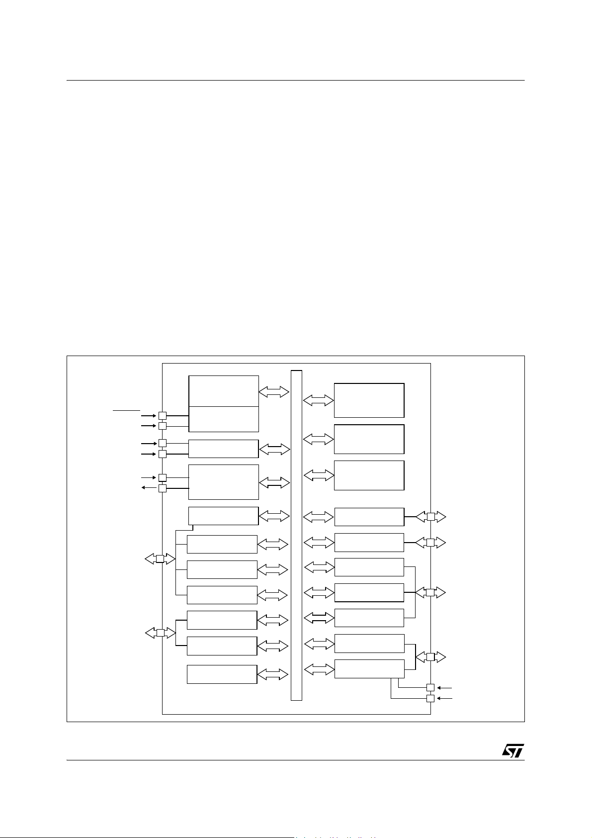
Figure 1. General Block Diagram
8-bit CORE
ALU
RESET
ISPSEL
V
DD
V
SS
CONTROL
LVD
-
-
-
Flash memory with byte-by-byte In-Situ Program
-
ming (ISP) capability.
Under software control, all devices can be placed
in Wait, Slow, Active Halt or Halt mode, reducing
power consumption when the application is in idle
or standby state.
The enhanced instruction set and addressing
modes of the ST7 offer both power and flexibility to
software developers, enabling the design of highly
efficient and compact application code. In addition
to standard 8-bit data management, all ST7 micro
controllers feature true bit manipulation, 8x8 unsigned multiplication and indirect addressing
modes.
For easy reference, all parametric data is located
Section 15 on page 108.
in
PROGRAM
MEMORY
(8 or 16 Kbytes)
RAM
(384 or 512 bytes)
OSC1
OSC2
PF7,6,4,2:0
(6-bit)
PE7:0
(6-bit for N versions)
(2-bit for J versions)
8/150
MULTI-OSC
+
CLOCK FILTER
MCC/RTC
PORT F
TIMER A
BEEP
PORT E
SCI
WATCHDOG
EEPROM
ADDRESS AND DATA BUS
(256 bytes)
PORT A
PORT B
PORT C
TIMER B
SPI
PORT D
8-bit ADC
PA7:0
(8-bit for N versions)
(5-bit for J versions)
PB7:0
(8-bit for N versions)
(5-bit for J versions)
PC7:0
(8-bit)
PD7:0
(8-bit for N versions)
(6-bit for J versions)
V
DDA
V
SSA
ST72334xx-Auto, ST72314xx-Auto, ST72124Jx-Auto
3 PIN DESCRIPTION
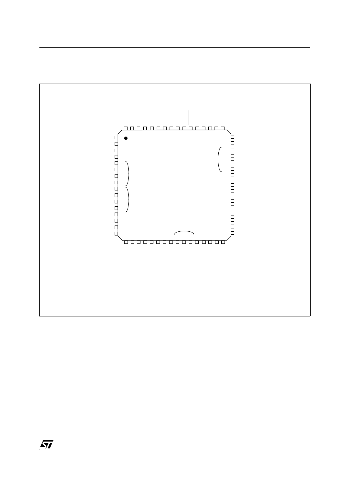
Figure 2. 64-Pin TQFP Package Pinout (N versions)
(HS) PE4
(HS) PE5
(HS) PE6
(HS) PE7
PB0
PB1
PB2
PB3
PB4
PB5
PB6
PB7
AIN0 / PD0
AIN1 / PD1
AIN2 / PD2
AIN3 / PD3
_2
DD
NCNCPE1 / RDI
64 63 62 61 60 59 58 57 56 55 54 53 52 51 50 49
1
V
PE0 / TDO
_2
SS
OSC1
OSC2
V
NCNCRESET
ISPSEL PA7 (HS)
PA6 (HS)
2
3
4
5
6
ei2
7
ei0
8
9
10
ei3
11
12
13
14
DD_3
V
ei1
SS_3
V
MCO / PF0
PF2
BEEP / PF1
NC
NC
15
16
17 18 19 20 21 22 23 24 29 30 31 3225 26 27 28
SSA
DDA
V
V
AIN4 / PD4
AIN5 / PD5
AIN6 / PD6
AIN7 / PD7
OCMP1_A / PF4
PA5 (HS)
46
45
44
43
ICAP1_A / (HS) PF6
PA4 (HS)
V
48
SS_1
V
47
DD_1
PA3
PA2
PA1
PA0
PC7 / SS
42
PC6 / SCK / ISPCLK
41
PC5 / MOSI
40
PC4 / MISO / ISPDATA
39
PC3 (HS) / ICAP1_B
38
PC2 (HS) / ICAP2_B
37
PC1 / OCMP1_B
36
PC0 / OCMP2_B
35
V
34
SS_0
V
33
DD_0
EXTCLK_A / (HS) PF7
(HS) 20mA high sink capability
associated external interrupt vector
ei
x
9/150
ST72334xx-Auto, ST72314xx-Auto, ST72124Jx-Auto
PIN DESCRIPTION (Cont’d)
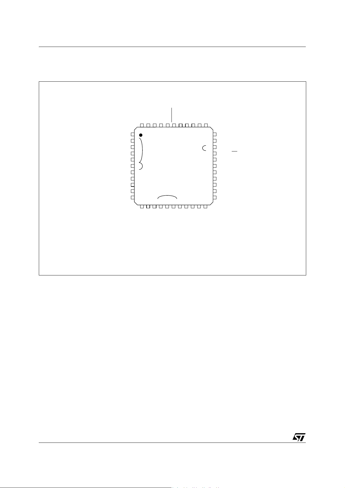
Figure 3. 44-Pin TQFP Package Pinout (J versions)
PE1 / RDI
PB0
PB1
PB2
PB3
PB4
AIN0 / PD0
AIN1 / PD1
AIN2 / PD2
AIN3 / PD3
AIN4 / PD4
_2
DD
PE0 / TDO
V
44 43 42 41 40 39 38 37 36 35 34
1
_2
SS
V
RESET
ISPSEL PA7 (HS)
OSC1
OSC2
PA6 (HS)
2
3
ei2
4
ei0
5
ei3
6
7
8
9
DDA
V
ei1
19 20 21 22
SSA
V
PF2
MCO / PF0
BEEP / PF1
10
11
12 13 14 15 16 17 18
AIN5 / PD5
OCMP1_A / PF4
ICAP1_A / (HS) PF6
EXTCLK_A / (HS) PF7
PA5 (HS)
DD_0
V
PA4 (HS)
V
33
SS_1
V
32
DD_1
PA3
31
PC7 / SS
30
PC6 / SCK / ISPCLK
29
PC5 / MOSI
28
PC4 / MISO / ISPDATA
27
PC3 (HS) / ICAP1_B
26
PC2 (HS) / ICAP2_B
25
PC1 / OCMP1_B
24
PC0 / OCMP2_B
23
SS_0
V
(HS) 20mA high sink capability
eixassociated external interrupt vector
10/150
ST72334xx-Auto, ST72314xx-Auto, ST72124Jx-Auto
PIN DESCRIPTION (Cont’d)
For external pin connection guidelines, refer to Section 15 "ELECTRICAL CHARACTERISTICS" on page
108.
Legend / Abbreviations for Table 1:
Type: I = input, O = output, S = supply
Input level: A = Dedicated analog input
In/Output level: C = CMOS 0.3VDD/0.7VDD,
CT= CMOS 0.3VDD/0.7VDD with input trigger
Output level: HS = 20mA high sink (on N-buffer only)
Port and control configuration:
– Input: float = floating, wpu = weak pull-up, int = interrupt
– Output: OD = open drain
2)
, PP = push-pull
Refer to Section 11 "I/O PORTS" on page 40 for more details on the software configuration of the I/O
ports.
The RESET configuration of each pin is shown in bold. This configuration is valid as long as the device is
in reset state.
Table 1. Device Pin Description
1)
, ana = analog
Pin
No.
TQFP64
Pin Name
TQFP44
Level Port
Type
Input
Input Output
Output
float
Main
function
(after
int
wpu
ana
OD
PP
reset)
1 - PE4 (HS) I/O CTHS X X X X Port E4
2 - PE5 (HS) I/O CTHS X X X X Port E5
3 - PE6 (HS) I/O CTHS X X X X Port E6
4 - PE7 (HS) I/O CTHS X X X X Port E7
5 2 PB0 I/O C
6 3 PB1 I/O C
7 4 PB2 I/O C
8 5 PB3 I/O C
9 6 PB4 I/O C
10 - PB5 I/O C
11 - PB6 I/O C
12 - PB7 I/O C
13 7 PD0/AIN0 I/O C
14 8 PD1/AIN1 I/O C
15 9 PD2/AIN2 I/O C
16 10 PD3/AIN3 I/O C
17 11 PD4/AIN4 I/O C
18 12 PD5/AIN5 I/O C
19 - PD6/AIN6 I/O C
20 - PD7/AIN7 I/O C
21 13 V
22 14 V
23 - V
DDA
SSA
DD_3
S Analog Power Supply Voltage
S Analog Ground Voltage
S Digital Main Supply Voltage
X ei2 X X Port B0
T
X ei2 X X Port B1
T
X ei2 X X Port B2
T
X ei2 X X Port B3
T
X ei3 X X Port B4
T
X ei3 X X Port B5
T
X ei3 X X Port B6
T
X ei3 X X Port B7
T
X X X X X Port D0 ADC Analog Input 0
T
X X X X X Port D1 ADC Analog Input 1
T
X X X X X Port D2 ADC Analog Input 2
T
X X X X X Port D3 ADC Analog Input 3
T
X X X X X Port D4 ADC Analog Input 4
T
X X X X X Port D5 ADC Analog Input 5
T
X X X X X Port D6 ADC Analog Input 6
T
X X X X X Port D7 ADC Analog Input 7
T
Alternate function
11/150
ST72334xx-Auto, ST72314xx-Auto, ST72124Jx-Auto
Pin
No.
Pin Name
TQFP64
TQFP44
24 - V
SS_3
25 15 PF0/MCO I/O C
26 16 PF1/BEEP I/O C
27 17 PF2 I/O C
Level Port
Type
Input
Input Output
Output
float
int
wpu
ana
OD
function
PP
Main
(after
reset)
Alternate function
S Digital Ground Voltage
X ei1 X X Port F0 Main clock output (f
T
X ei1 X X Port F1 Beep signal output
T
X ei1 X X Port F2
T
OSC
/2)
28 - NC Not Connected
29 18 PF4/OCMP1_A I/O C
X X X X Port F4 Timer A Output Compare 1
T
30 - NC Not Connected
31 19 PF6 (HS)/ICAP1_A I/O CTHS X X X X Port F6 Timer A Input Capture 1
32 20 PF7 (HS)/EXTCLK_A I/O CTHS X X X X Port F7 Timer A External Clock Source
33 21 V
34 22 V
DD_0
SS_0
35 23 PC0/OCMP2_B I/O C
36 24 PC1/OCMP1_B I/O C
S Digital Main Supply Voltage
S Digital Ground Voltage
X X X X Port C0 Timer B Output Compare 2
T
X X X X Port C1 Timer B Output Compare 1
T
37 25 PC2 (HS)/ICAP2_B I/O CTHS X X X X Port C2 Timer B Input Capture 2
38 26 PC3 (HS)/ICAP1_B I/O CTHS X X X X Port C3 Timer B Input Capture 1
39 27 PC4/MISO I/O C
40 28 PC5/MOSI I/O C
41 29 PC6/SCK I/O C
42 30 PC7/SS I/O C
43 - PA0 I/O C
44 - PA1 I/O C
45 - PA2 I/O C
46 31 PA3 I/O C
47 32 V
48 33 V
DD_1
SS_1
S Digital Main Supply Voltage
S Digital Ground Voltage
X X X X Port C4 SPI Master In / Slave Out Data
T
X X X X Port C5 SPI Master Out / Slave In Data
T
X X X X Port C6 SPI Serial Clock
T
X X X X Port C7 SPI Slave Select (active low)
T
X ei0 X X Port A0
T
X ei0 X X Port A1
T
X ei0 X X Port A2
T
X ei0 X X Port A3
T
49 34 PA4 (HS) I/O CTHS X X X X Port A4
50 35 PA5 (HS) I/O CTHS X X X X Port A5
51 36 PA6 (HS) I/O CTHS X T Port A6
52 37 PA7 (HS) I/O CTHS X T Port A7
Must be tied low in user mode. In programming
53 38 ISPSEL I
mode when available, this pin acts as In-Situ
Programming mode selection.
54 39 RESET I/O C X X Top priority non maskable interrupt (active low)
55 - NC
56 - NC
57 40 V
SS_3
58 41 OSC2
59 42 OSC1
60 43 V
DD_3
S Digital Ground Voltage
3)
3)
O
I
S Digital Main Supply Voltage
Not Connected
Resonator oscillator inverter output or capacitor input for RC oscillator
External clock input or Resonator oscillator inverter input or resistor input for RC oscillator
12/150

ST72334xx-Auto, ST72314xx-Auto, ST72124Jx-Auto
Pin
No.
Pin Name
TQFP64
TQFP44
61 44 PE0/TDO I/O C
62 1 PE1/RDI I/O C
63 - NC
64 - NC
Level Port
Type
Input
T
T
Input Output
Output
float
X X X X Port E0 SCI Transmit Data Out
X X X X Port E1 SCI Receive Data In
Main
function
(after
int
wpu
ana
OD
reset)
PP
Not Connected
Alternate function
Notes:
1. In the interrupt input column, “eix” defines the associated external interrupt vector. If the weak pull-up
column (wpu) is merged with the interrupt column (int), then the I/O configuration is pull-up interrupt input,
else the configuration is floating interrupt input.
2. In the open drain output column, “T” defines a true open drain I/O (P-Buffer and protection diode to V
are not implemented). See Section 11 "I/O PORTS" on page 40 and Section 15.8 "I/O PORT PIN CHAR-
DD
ACTERISTICS" on page 129 for more details.
3. OSC1 and OSC2 pins connect a crystal or ceramic resonator, an external RC, or an external source to
the on-chip oscillator see
Section 3 "PIN DESCRIPTION" on page 9 and Section 15.5 "CLOCK AND TIM-
ING CHARACTERISTICS" on page 117 for more details.
13/150
ST72334xx-Auto, ST72314xx-Auto, ST72124Jx-Auto
4 REGISTER AND MEMORY MAP
As shown in the Figure 4, the MCU is capable of
addressing 64 Kbytes of memories and I/O registers.
The available memory locations consist of 128
bytes of register locations, 384 or 512 bytes of
RAM, up to 256 bytes of data EEPROM and 4 or
Kbytes of user program memory. The RAM
8
Figure 4. Memory Map
0000h
007Fh
0080h
01FFh
027Fh
0200h / 0280h
0BFFh
0C00h
0CFFh
0D00h
BFFFh
C000h
E000h
FFDFh
FFE0h
FFFFh
HW Registers
(see Table 2)
384 bytes RAM
512 bytes RAM
Reserved
256 bytes Data EEPROM
Reserved
16 Kbytes
8 Kbytes
Program
Memory
Interrupt and Reset Vectors
(see Table 6 on page 35)
Program
Memory
space includes up to 256 bytes for the stack from
0100h to 01FFh.
The highest address bytes contain the user reset
and interrupt vectors.
IMPORTANT: Memory locations marked as “Reserved” must never be accessed. Accessing a reserved area can have unpredictable effects on the
device.
0080h
00FFh
0100h
01FFh
0080h
00FFh
0100h
01FFh
0200h
027Fh
C000h
E000h
FFFFh
Short Addressing RAM
Zero page
(128 bytes)
Stack or
16-bit Addressing RAM
(256 bytes)
Short Addressing RAM
Zero page
(128 bytes)
Stack or
16-bit Addressing RAM
(256 bytes)
16-bit Addressing
RAM
16 Kbytes
8 Kbytes
14/150

REGISTER AND MEMORY MAP (Cont’d)
Table 2. Hardware Register Map
ST72334xx-Auto, ST72314xx-Auto, ST72124Jx-Auto
Address Block
0000h
0001h
Port A
0002h
Register
Label
PADR
PADDR
PAOR
Register Name
Port A Data Register
Port A Data Direction Register
Port A Option Register
0003h Reserved Area (1 byte)
0004h
0005h
0006h
Port C
PCDR
PCDDR
PCOR
Port C Data Register
Port C Data Direction Register
Port C Option Register
0007h Reserved Area (1 byte)
0008h
0009h
000Ah
Port B
PBDR
PBDDR
PBOR
Port B Data Register
Port B Data Direction Register
Port B Option Register
000Bh Reserved Area (1 byte)
000Ch
000Dh
000Eh
Port E
PEDR
PEDDR
PEOR
Port E Data Register
Port E Data Direction Register
Port E Option Register
000Fh Reserved Area (1 byte)
0010h
0011h
0012h
Port D
PDDR
PDDDR
PDOR
Port D Data Register
Port D Data Direction Register
Port D Option Register
Reset
Status
1)
00h
00h
00h
1)
00h
00h
00h
1)
00h
00h
00h
1)
00h
00h
00h
1)
00h
00h
00h
Remarks
R/W
R/W
2)
R/W
R/W
R/W
R/W
R/W
R/W
2)
R/W
R/W
R/W
2)
R/W
R/W
R/W
2)
R/W
0013h Reserved Area (1 byte)
0014h
0015h
0016h
Port F
PFDR
PFDDR
PFOR
Port F Data Register
Port F Data Direction Register
Port F Option Register
00h
00h
00h
1)
R/W
R/W
R/W
0017h
to
Reserved Area (9 bytes)
001Fh
0020h MISCR1 Miscellaneous Register 1 00h R/W
0021h
0022h
0023h
SPI
SPIDR
SPICR
SPISR
SPI Data I/O Register
SPI Control Register
SPI Status Register
xxh
0xh
00h
R/W
R/W
Read Only
0024h
to
Reserved Area (5 bytes)
0028h
0029h MCC MCCSR Main Clock Control / Status Register 01h R/W
15/150
ST72334xx-Auto, ST72314xx-Auto, ST72124Jx-Auto
Address Block
Register
Label
Register Name
Reset
Status
002Ah WATCHDOG WDGCR Watchdog Control Register 7Fh R/W
002Bh CRSR Clock, Reset, Supply Control / Status Register 000x 000x R/W
002Ch Data-EEPROM EECSR Data-EEPROM Control/Status Register 00h R/W
002Dh
0030h
0031h
0032h
0033h
0034h
0035h
0036h
0037h
0038h
0039h
003Ah
003Bh
003Ch
003Dh
003Eh
003Fh
TIMER A
TACR2
TACR1
TASR
TAIC1HR
TAIC1LR
TAOC1HR
TAOC1LR
TACHR
TACLR
TAACHR
TAACLR
TAIC2HR
TAIC2LR
TAOC2HR
TAOC2LR
Timer A Control Register 2
Timer A Control Register 1
Timer A Status Register
Timer A Input Capture 1 High Register
Timer A Input Capture 1 Low Register
Timer A Output Compare 1 High Register
Timer A Output Compare 1 Low Register
Timer A Counter High Register
Timer A Counter Low Register
Timer A Alternate Counter High Register
Timer A Alternate Counter Low Register
Timer A Input Capture 2 High Register
Timer A Input Capture 2 Low Register
Timer A Output Compare 2 High Register
Timer A Output Compare 2 Low Register
Reserved Area (4 bytes)
00h
00h
xxh
xxh
xxh
80h
00h
FFh
FCh
FFh
FCh
xxh
xxh
80h
00h
Remarks
R/W
R/W
Read Only
Read Only
Read Only
R/W
R/W
Read Only
Read Only
Read Only
Read Only
Read Only 3)
Read Only
R/W
R/W
3)
3)
3)
0040h MISCR2 Miscellaneous Register 2 00h R/W
0041h
0042h
0043h
0044h
0045h
0046h
0047h
0048h
0049h
004Ah
004Bh
004Ch
004Dh
004Eh
004Fh
0050h
0051h
0052h
0053h
0054h
0055h
0056h
0057h
0058h
006Fh
TIMER B
SCI
TBCR2
TBCR1
TBSR
TBIC1HR
TBIC1LR
TBOC1HR
TBOC1LR
TBCHR
TBCLR
TBACHR
TBACLR
TBIC2HR
TBIC2LR
TBOC2HR
TBOC2LR
SCISR
SCIDR
SCIBRR
SCICR1
SCICR2
SCIERPR
SCIETPR
Timer B Control Register 2
Timer B Control Register 1
Timer B Status Register
Timer B Input Capture 1 High Register
Timer B Input Capture 1 Low Register
Timer B Output Compare 1 High Register
Timer B Output Compare 1 Low Register
Timer B Counter High Register
Timer B Counter Low Register
Timer B Alternate Counter High Register
Timer B Alternate Counter Low Register
Timer B Input Capture 2 High Register
Timer B Input Capture 2 Low Register
Timer B Output Compare 2 High Register
Timer B Output Compare 2 Low Register
SCI Status Register
SCI Data Register
SCI Baud Rate Register
SCI Control Register 1
SCI Control Register 2
SCI Extended Receive Prescaler Register
Reserved area
SCI Extended Transmit Prescaler Register
Reserved Area (24 bytes)
00h
00h
xxh
xxh
xxh
80h
00h
FFh
FCh
FFh
FCh
xxh
xxh
80h
00h
C0h
xxh
00xx xxxx
xxh
00h
00h
---
00h
R/W
R/W
Read Only
Read Only
Read Only
R/W
R/W
Read Only
Read Only
Read Only
Read Only
Read Only
Read Only
R/W
R/W
Read Only
R/W
R/W
R/W
R/W
R/W
R/W
16/150

ST72334xx-Auto, ST72314xx-Auto, ST72124Jx-Auto
Address Block
0070h
0071h
0072h
to
007Fh
ADC
Register
Label
ADCDR
ADCCSR
Register Name
Data Register
Control/Status Register
Reserved Area (14 bytes)
Reset
Status
xxh
00h
Remarks
Read Only
R/W
Legend: x=undefined, R/W=read/write
Notes:
1. The contents of the I/O port DR registers are readable only in output configuration. In input configuration, the values
of the I/O pins are returned instead of the DR register contents.
2. The bits corresponding to unavailable pins are forced to 1 by hardware, affecting accordingly the reset status value.
These bits must always keep their reset value.
3. External pin not available.
17/150
ST72334xx-Auto, ST72314xx-Auto, ST72124Jx-Auto
5 FLASH PROGRAM MEMORY
5.1 INTRODUCTION
Flash devices have a single voltage non-volatile
Flash memory that may be programmed in-situ (or
plugged in a programming tool) on a byte-by-byte
basis.
5.2 MAIN FEATURES
■ Remote In-Situ Programming (ISP) mode
■ Up to 16 bytes programmed in the same cycle
■ MTP memory (Multiple Time Programmable)
■ Readout memory protection against piracy
5.3 STRUCTURAL ORGANIZATION
The Flash program memory is organized in a single 8-bit wide memory block which can be used for
storing both code and data constants.
The Flash program memory is mapped in the upper part of the ST7 addressing space and includes
the reset and interrupt user vector area.
5.4 IN-SITU PROGRAMMING (ISP) MODE
The Flash program memory can be programmed
using Remote ISP mode. This ISP mode allows
the contents of the ST7 program memory to be up
dated using a standard ST7 programming tools after the device is mounted on the application board.
This feature can be implemented with a minimum
number of added components and board area im
pact.
An example Remote ISP hardware interface to the
standard ST7 programming tool is described be
low. For more details on ISP programming, refer to
the ST7 Programming Specification.
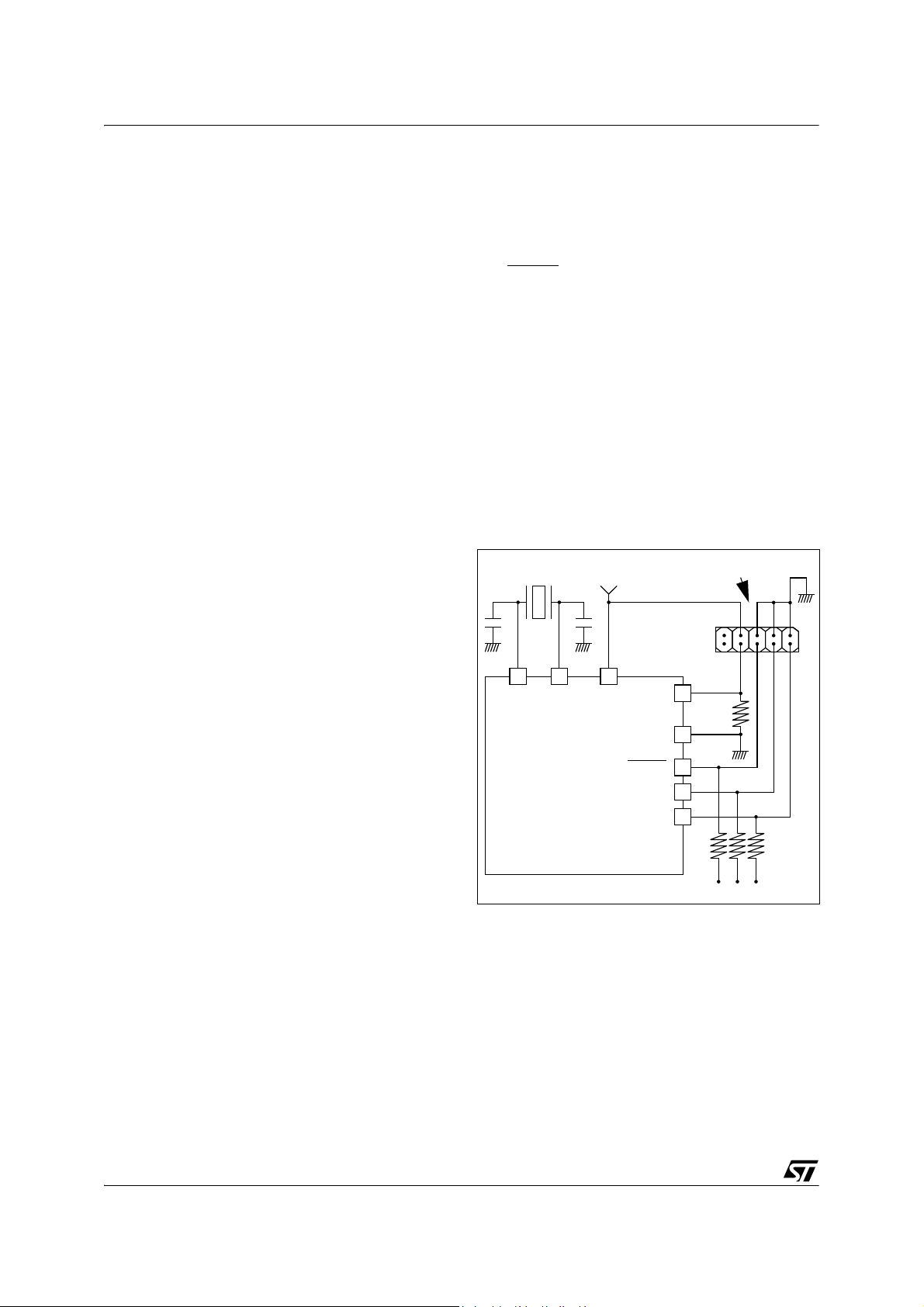
Remote ISP Overview
The Remote ISP mode is initiated by a specific sequence on the dedicated ISPSEL pin.
The Remote ISP is performed in three steps:
– Selection of the RAM execution mode
– Download of Remote ISP code in RAM
– Execution of Remote ISP code in RAM to pro-
gram the user program into the Flash
Remote ISP hardware configuration
In Remote ISP mode, the ST7 has to be supplied
with power (V
and VSS) and a clock signal (os-
DD
cillator and application crystal circuit for example).
This mode needs five signals (plus the VDD signal
if necessary) to be connected to the programming
tool. This signals are:
– RESET: device reset
–VSS: device ground power supply
– ISPCLK: ISP output serial clock pin
– ISPDATA: ISP input serial data pin
– ISPSEL: Remote ISP mode selection. This pin
must be connected to V
board through a pull-down resistor.
on the application
SS
If any of these pins are used for other purposes on
the application, a serial resistor has to be imple
mented to avoid a conflict if the other device forces
the signal level.
Figure 5 shows a typical hardware interface to a
standard ST7 programming tool. For more details
on the pin locations, refer to the device pinout de
scription.
Figure 5. Typical Remote ISP Interface
HE10 CONNECTOR TYPE
XTAL
C
L0
C
L1
-
OSC1
OSC2
TO PROGRAMMING TOOL
ISPSEL
DD
V
V
10KΩ
SS
-
RESET
-
ST7
ISPCLK
ISPDATA
APPLICATION
5.5 MEMORY READOUT PROTECTION
The readout protection is enabled through an option bit.
For Flash devices, when this option is selected,
the program and data stored in the Flash memory
are protected against readout piracy (including a
re-write protection). When this protection option is
removed the entire Flash program memory is first
automatically erased. However, the EEPROM
data memory (when available) can be protected
only with ROM devices.
-
-
1
47KΩ
18/150
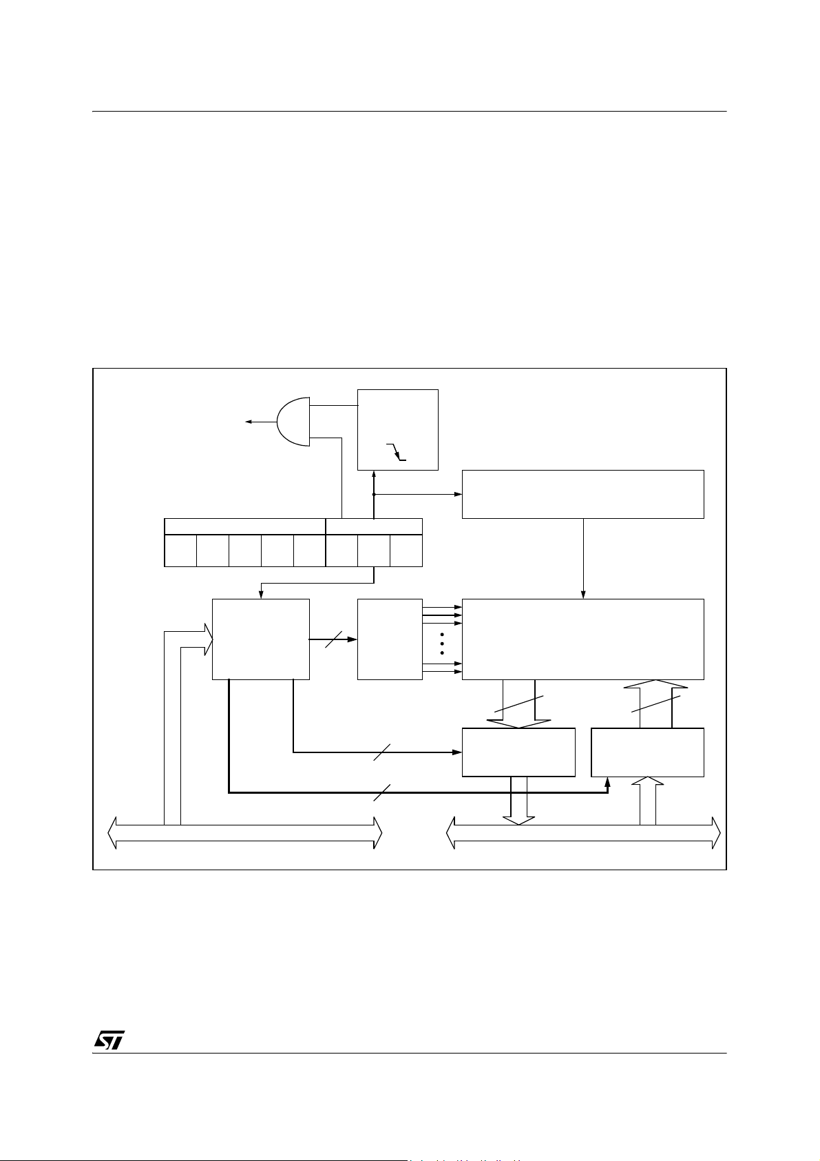
6 DATA EEPROM
ST72334xx-Auto, ST72314xx-Auto, ST72124Jx-Auto
6.1 INTRODUCTION
The Electrically Erasable Programmable Read
Only Memory can be used as a non-volatile backup for storing data. Using the EEPROM requires a
basic access protocol described in this chapter.
Figure 6. EEPROM Block Diagram
FALLING
EEPROM INTERRUPT
EECSR
IE LAT00 0 0 0 PGM
EDGE
DETECTOR
EEPROMRESERVED
6.2 MAIN FEATURES
■ Up to 16 bytes programmed in the same cycle
■ EEPROM mono-voltage (charge pump)
■ Chained erase and programming cycles
■ Internal control of the global programming cycle
duration
■ End of programming cycle interrupt flag
■ Wait mode management
HIGH VOLTAGE
PUMP
ADDRESS
DECODER
ADDRESS BUS
4
ROW
DECODER
4
4
MEMORY MATRIX
(1 ROW = 16 x 8 BITS)
DATA
MULTIPLEXER
EEPROM
128128
16 x 8 BITS
DATA LATCHES
DATA BUS
19/150
ST72334xx-Auto, ST72314xx-Auto, ST72124Jx-Auto
DATA EEPROM (Cont’d)
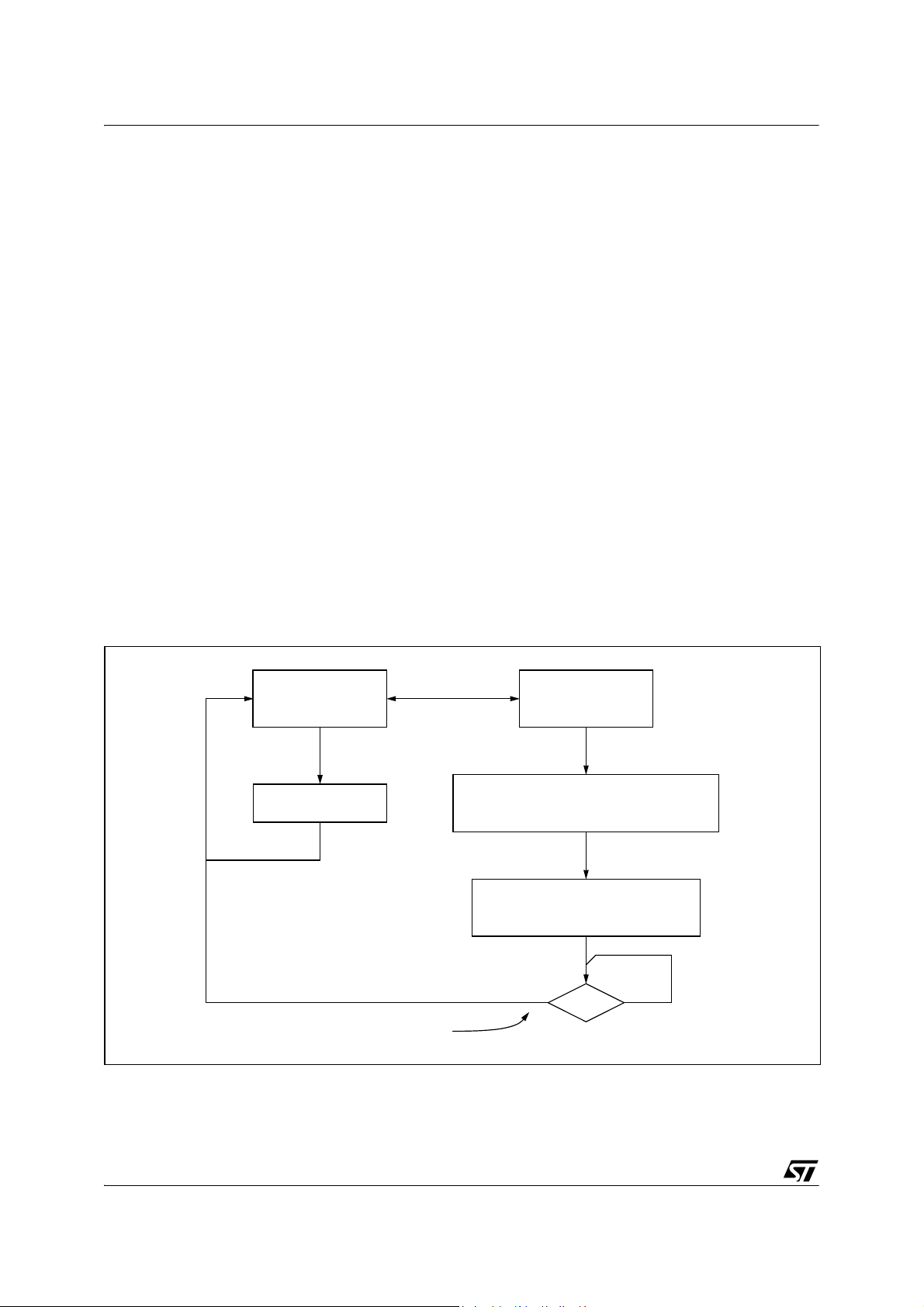
6.3 MEMORY ACCESS
The Data EEPROM memory read/write access
modes are controlled by the LAT bit of the EEP
ROM Control/Status register (EECSR). The flowchart in Figure 7 describes these different memory
access modes.
Read Operation (LAT=0)
The EEPROM can be read as a normal ROM location when the LAT bit of the EECSR register is
cleared. In a read cycle, the byte to be accessed is
put on the data bus in less than 1 CPU clock cycle.
This means that reading data from EEPROM
takes the same time as reading data from
EPROM, but this memory cannot be used to exe
cute machine code.
Write Operation (LAT=1)
To access the write mode, the LAT bit has to be
set by software (the PGM bit remains cleared).
When a write access to the EEPROM area occurs,
the value is latched inside the 16 data latches ac
cording to its address.
Figure 7. Data EEPROM Programming Flowchart
When PGM bit is set by the software, all the previous bytes written in the data latches (up to 16) are
programmed in the EEPROM cells. The effective
high address (row) is determined by the last EEP
ROM write sequence. To avoid wrong programming, the user must take care that all the bytes
written between two programming sequences
have the same high address: only the four Least
Significant Bits of the address can change.
At the end of the programming cycle, the PGM and
LAT bits are cleared simultaneously, and an inter
rupt is generated if the IE bit is set. The Data EEPROM interrupt request is cleared by hardware
when the Data EEPROM interrupt vector is
fetched.
Note: Care should be taken during the programming cycle. Writing to the same memory location
will over-program the memory (logical AND be
tween the two write access data result) because
the data latches are only cleared at the end of the
programming cycle and by the falling edge of LAT
bit.
It is not possible to read the latched data.
This note is illustrated by the Figure 8.
READ MODE
LAT=0
PGM=0
READ BYTES
IN EEPROM AREA
INTERRUPT GENERATION
IF IE=1 0 1
CLEARED BY HARDWARE
WRITE MODE
LAT=1
PGM=0
WRITE UP TO 16 BYTES
IN EEPROM AREA
(with the same 11 MSB of the address)
START PROGRAMMING CYCLE
LAT=1
PGM=1 (set by software)
LAT
20/150
DATA EEPROM (Cont’d)
ST72334xx-Auto, ST72314xx-Auto, ST72124Jx-Auto
6.4 POWER SAVING MODES
Wait mode
The Data EEPROM can enter Wait mode on execution of the WFI instruction of the microcontroller.
The Data EEPROM will immediately enter this
mode if there is no programming in progress, oth
erwise the Data EEPROM will finish the cycle and
then enter Wait mode.
Halt mode
The Data EEPROM immediately enters Halt mode
if the microcontroller executes the HALT instruc
tion. Therefore the EEPROM will stop the function
in progress, and data may be corrupted.
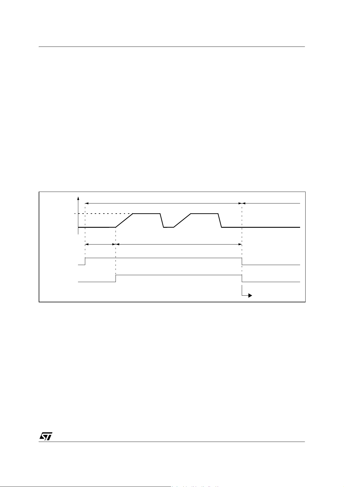
Figure 8. Data EEPROM Programming Cycle
READ OPERATION NOT POSSIBLE
INTERNAL
PROGRAMMING
VOLTAGE
ERASE CYCLE WRITE CYCLE
WRITE OF
DATA LATCHES
6.5 ACCESS ERROR HANDLING
If a read access occurs while LAT=1, then the data
bus will not be driven.
If a write access occurs while LAT=0, then the
data on the bus will not be latched.
If a programming cycle is interrupted (by software/
RESET action), the memory data will not be guar
anteed.
READ OPERATION POSSIBLE
t
PROG
-
EEPROM INTERRUPT
LAT
PGM
21/150

ST72334xx-Auto, ST72314xx-Auto, ST72124Jx-Auto
DATA EEPROM (Cont’d)
6.6 REGISTER DESCRIPTION
Bit 1 = LAT Latch Access Transfer
This bit is set by software. It is cleared by hard-
CONTROL/STATUS REGISTER (CSR)
Read / Write
Reset Value: 0000 0000 (00h)
7 0
ware at the end of the programming cycle. It can
only be cleared by software if PGM bit is cleared.
0: Read mode
1: Write mode
Bit 0 = PGM Programming control and status
0 0 0 0 0 IE LAT PGM
This bit is set by software to begin the programming
cycle. At the end of the programming cycle, this bit
is cleared by hardware and an interrupt is generated
Bit 7:3 = Reserved, forced by hardware to 0.
if the ITE bit is set.
0: Programming finished or not yet started
1: Programming cycle is in progress
Bit 2 = IE Interrupt enable
This bit is set and cleared by software. It enables the
Data EEPROM interrupt capability when the PGM
bit is cleared by hardware. The interrupt request is
Note: if the PGM bit is cleared during the programming cycle, the memory data is not guaranteed
automatically cleared when the software enters the
interrupt routine.
0: Interrupt disabled
1: Interrupt enabled
Table 3. Data EEPROM Register Map and Reset Values
Address
(Hex.)
002Ch
Register
Label
EECSR
Reset Value 0 0 0 0 0
7 6 5 4 3 2 1 0
IE
0
RWM
0
PGM
0
6.7 READOUT PROTECTION OPTION
The Data EEPROM can be optionally readout protected in ST72334 ROM devices (see option list on
22/150
page 145). ST72C334 Flash devices do not have
this protection option.
7 CENTRAL PROCESSING UNIT
ST72334xx-Auto, ST72314xx-Auto, ST72124Jx-Auto
7.1 INTRODUCTION
This CPU has a full 8-bit architecture and contains
six internal registers allowing efficient 8-bit data
manipulation.
7.2 MAIN FEATURES
■ 63 basic instructions
■ Fast 8-bit by 8-bit multiply
■ 17 main addressing modes
■ Two 8-bit index registers
■ 16-bit stack pointer
■ Low power modes
■ Maskable hardware interrupts
■ Non-maskable software interrupt
7.3 CPU REGISTERS
The six CPU registers shown in Figure 9 are not
present in the memory mapping and are accessed
by specific instructions.
Figure 9. CPU Registers
70
RESET VALUE = XXh
70
RESET VALUE = XXh
70
RESET VALUE = XXh
Accumulator (A)
The Accumulator is an 8-bit general purpose register used to hold operands and the results of the
arithmetic and logic calculations and to manipulate
data.
Index Registers (X and Y)
In indexed addressing modes, these 8-bit registers
are used to create either effective addresses or
temporary storage areas for data manipulation.
(The Cross-Assembler generates a precede in
struction (PRE) to indicate that the following instruction refers to the Y register.)
The Y register is not affected by the interrupt automatic procedures (not pushed to and popped from
the stack).
Program Counter (PC)
The program counter is a 16-bit register containing
the address of the next instruction to be executed
by the CPU. It is made of two 8-bit registers PCL
(Program Counter Low which is the LSB) and PCH
(Program Counter High which is the MSB).
ACCUMULATOR
X INDEX REGISTER
Y INDEX REGISTER
-
15 8
RESET VALUE = RESET VECTOR @ FFFEh-FFFFh
15
RESET VALUE = STACK HIGHER ADDRESS
PCH
RESET VALUE =
7
70
1C11HI NZ
1X11X1XX
70
8
PCL
0
PROGRAM COUNTER
CONDITION CODE REGISTER
STACK POINTER
X = Undefined Value
23/150

ST72334xx-Auto, ST72314xx-Auto, ST72124Jx-Auto
CPU REGISTERS (Cont’d)
CONDITION CODE REGISTER (CC)
Read/Write
Reset Value: 111x1xxx
7 0
1 1 1 H I N Z C
The 8-bit Condition Code register contains the interrupt mask and four flags representative of the
result of the instruction just executed. This register
can also be handled by the PUSH and POP in
structions.
These bits can be individually tested and/or controlled by specific instructions.
Bit 4 = H Half carry
This bit is set by hardware when a carry occurs be-
tween bits 3 and 4 of the ALU during an ADD or
ADC instruction. It is reset by hardware during the
same instructions.
0: No half carry has occurred.
1: A half carry has occurred.
This bit is tested using the JRH or JRNH instruction. The H bit is useful in BCD arithmetic subroutines.
Bit 3 = I Interrupt mask
This bit is set by hardware when entering in interrupt or by software to disable all interrupts except
the TRAP software interrupt. This bit is cleared by
software.
0: Interrupts are enabled.
1: Interrupts are disabled.
This bit is controlled by the RIM, SIM and IRET instructions and is tested by the JRM and JRNM instructions.
Note: Interrupts requested while I is set are
latched and can be processed when I is cleared.
By default an interrupt routine is not interruptible
because the I bit is set by hardware at the start of
the routine and reset by the IRET instruction at the
end of the routine. If the I bit is cleared by software
in the interrupt routine, pending interrupts are
serviced regardless of the priority level of the cur
rent interrupt routine.
Bit 2 = N Negative
This bit is set and cleared by hardware. It is repre-
sentative of the result sign of the last arithmetic,
logical or data manipulation. It is a copy of the 7
bit of the result.
0: The result of the last operation is positive or null.
1: The result of the last operation is negative
(that is, the most significant bit is a logic 1).
This bit is accessed by the JRMI and JRPL instructions.
-
Bit 1 = Z Zero
This bit is set and cleared by hardware. This bit indicates that the result of the last arithmetic, logical
or data manipulation is zero.
0: The result of the last operation is different from
zero.
1: The result of the last operation is zero.
This bit is accessed by the JREQ and JRNE test
instructions.
Bit 0 = C Carry/borrow
This bit is set and cleared by hardware and soft-
ware. It indicates an overflow or an underflow has
occurred during the last arithmetic operation.
0: No overflow or underflow has occurred.
1: An overflow or underflow has occurred.
This bit is driven by the SCF and RCF instructions
and tested by the JRC and JRNC instructions. It is
also affected by the “bit test and branch”, shift and
rotate instructions.
-
th
24/150
ST72334xx-Auto, ST72314xx-Auto, ST72124Jx-Auto
CENTRAL PROCESSING UNIT (Cont’d)
Stack Pointer (SP)
Read/Write
Reset Value: 01 FFh
15 8
0 0 0 0 0 0 0 1
7 0
SP7 SP6 SP5 SP4 SP3 SP2 SP1 SP0
The Stack Pointer is a 16-bit register which is always pointing to the next free location in the stack.
It is then decremented after data has been pushed
onto the stack and incremented before data is
popped from the stack (see
Since the stack is 256 bytes deep, the 8th most
significant bits are forced by hardware. Following
an MCU Reset, or after a Reset Stack Pointer in
struction (RSP), the Stack Pointer contains its reset value (the SP7 to SP0 bits are set) which is the
stack higher address.
Figure 10).
-
The least significant byte of the Stack Pointer
(called S) can be directly accessed by a LD in
-
struction.
Note: When the lower limit is exceeded, the Stack
Pointer wraps around to the stack upper limit, with
out indicating the stack overflow. The previously
stored information is then overwritten and there
fore lost. The stack also wraps in case of an underflow.
The stack is used to save the return address during a subroutine call and the CPU context during
an interrupt. The user may also directly manipulate
the stack by means of the PUSH and POP instruc
tions. In the case of an interrupt, the PCL is stored
at the first location pointed to by the SP. Then the
other registers are stored in the next locations as
shown in
Figure 10.
– When an interrupt is received, the SP is decre-
mented and the context is pushed on the stack.
– On return from interrupt, the SP is incremented
and the context is popped from the stack.
A subroutine call occupies two locations and an interrupt five locations in the stack area.
Figure 10. Stack Manipulation Example
@ 0100h
SP
@ 01FFh
CALL
Subroutine
SP
PCH
PCL
Stack Higher Address = 01FFh
Stack Lower Address =
Interrupt
Event
SP
CC
A
X
PCH
PCL
PCH
PCL
0100h
PUSH Y POP Y IRET
SP
Y
CC
A
X
PCH
PCL
PCH
PCL
CC
A
X
PCH
PCL
PCH
PCL
SP
PCH
PCL
RET
or RSP
SP
25/150
ST72334xx-Auto, ST72314xx-Auto, ST72124Jx-Auto
8 SUPPLY, RESET AND CLOCK MANAGEMENT
The ST72334J/N-Auto, ST72314J/N-Auto and
ST72124J-Auto microcontrollers include a range
of utility features for securing the application in crit
ical situations (for example, in case of a power
brown-out), and reducing the number of external
components. An overview is shown in
Figure 11.
See Section 15 "ELECTRICAL CHARACTERIS-
TICS" on page 108 for more details.
Main Features
■ Supply Manager with main supply low voltage
detection (LVD)
■ Reset Sequence Manager (RSM)
Figure 11. Clock, Reset and Supply Block Diagram
CLOCK SECURITY SYSTEM
(CSS)
OSC2
OSC1
MULTI-
OSCILLATOR
(MO)
CLOCK
FILTER
■ Multi-Oscillator (MO)
– 4 Crystal/Ceramic resonator oscillators
– 1 External RC oscillator
– 1 Internal RC oscillator
■ Clock Security System (CSS)
– Clock Filter
– Backup Safe Oscillator
SAFE
OSC
f
OSC
TO
MAIN CLOCK
CONTROLLER
RESET
V
DD
V
SS
RESET SEQUENCE
MANAGER
(RSM)
LOW VOLTAGE
DETECTOR
(LVD)
CRSR
FROM
WATCHDOG
PERIPHERAL
LVD
IE D00 0 0 RF RF
CSS INTERRUPT
CSS WDG
26/150
8.1 LOW VOLTAGE DETECTOR (LVD)
ST72334xx-Auto, ST72314xx-Auto, ST72124Jx-Auto
To allow the integration of power management
features in the application, the Low Voltage Detec
tor function (LVD) generates a static reset when
the V
supply voltage is below a V
DD
reference
IT-
value. This means that it secures the power-up as
well as the power-down keeping the ST7 in reset.
The V
than the V
to avoid a parasitic reset when the MCU starts run
reference value for a voltage drop is lower
IT-
reference value for power-on in order
IT+
ning and sinks current on the supply (hysteresis).
The LVD Reset circuitry generates a reset when
is below:
V
DD
–V
when VDD is rising
IT+
–V
when VDD is falling
IT-
The LVD function is illustrated in the Figure 12.
Provided the minimum VDD value (guaranteed for
the oscillator frequency) is above V
, the MCU
IT-
can only be in two modes:
– under full software control
– in static safe reset
Figure 12. Low Voltage Detector vs Reset
V
DD
In these conditions, secure operation is always ensured for the application without the need for external reset hardware.
During a Low Voltage Detector Reset, the RESET
pin is held low, thus permitting the MCU to reset
other devices.
Notes:
1. The LVD allows the device to be used without
any external RESET circuitry.
2. Three different reference levels are selectable
through the option byte according to the applica
tion requirement.
LVD application note
Application software can detect a reset caused by
the LVD by reading the LVDRF bit in the CRSR
register.
This bit is set by hardware when a LVD reset is
generated and cleared by software (writing zero).
-
V
IT+
V
IT-
RESET
V
hyst
27/150
ST72334xx-Auto, ST72314xx-Auto, ST72124Jx-Auto
8.2 RESET SEQUENCE MANAGER (RSM)
8.2.1 Introduction
The reset sequence manager includes three RESET sources as shown in Figure 14:
■ External RESET source pulse
■ Internal LVD RESET (Low Voltage Detection)
■ Internal WATCHDOG RESET
These sources act on the RESET pin and it is always kept low during the delay phase.
The RESET service routine vector is fixed at addresses FFFEh-FFFFh in the ST7 memory map.
The basic RESET sequence consists of three
phases as shown in
■ Delay depending on the RESET source
■ 4096 CPU clock cycle delay
■ RESET vector fetch
Figure 13:
Figure 14. Reset Block Diagram
V
DD
f
CPU
The 4096 CPU clock cycle delay allows the oscillator to stabilise and ensures that recovery has
taken place from the Reset state.
The RESET vector fetch phase duration is 2 clock
cycles.
Figure 13. RESET Sequence Phases
RESET
DELAY
INTERNAL RESET
4096 CLOCK CYCLES
FETCH
VECTOR
INTERNAL
RESET
RESET
R
ON
COUNTER
WATCHDOG RESET
LVD RESET
28/150
RESET SEQUENCE MANAGER (Cont’d)
ST72334xx-Auto, ST72314xx-Auto, ST72124Jx-Auto
8.2.2 Asynchronous External RESET Pin
The RESET pin is both an input and an open-drain
output with integrated R
This pull-up has no fixed value but varies in ac
weak pull-up resistor.
ON
cordance with the input voltage. It can be pulled
low by external circuitry to reset the device. See
ELECTRICAL CHARACTERISTICS section for
more details.
A RESET signal originating from an external
source must have a duration of at least t
h(RSTL)in
order to be recognized. This detection is asynchro
in
nous and therefore the MCU can enter reset state
even in Halt mode.
The RESET pin is an asynchronous signal which
plays a major role in EMS performance. In a noisy
environment, it is recommended to follow the
guidelines mentioned in the
ELECTRICAL CHAR-
ACTERISTICS section.
Two RESET sequences can be associated with
this RESET source: short or long external reset
pulse (see
Figure 15).
Starting from the external RESET pulse recognition, the device RESET pin acts as an output that
is pulled low during at least t
w(RSTL)out
.
Figure 15. RESET Sequences
8.2.3 Internal Low Voltage Detection RESET
Two different RESET sequences caused by the internal LVD circuitry can be distinguished:
■ Power-On RESET
■ Voltage Drop RESET
The device RESET pin acts as an output that is
pulled low when V
V
DD<VIT-
(falling edge) as shown in Figure 15.
DD<VIT+
The LVD filters spikes on V
(rising edge) or
larger than t
DD
g(VDD)
to
avoid parasitic resets.
8.2.4 Internal Watchdog RESET
The RESET sequence generated by an internal
Watchdog counter overflow is shown in
Figure 15.
Starting from the Watchdog counter underflow, the
device
low during at least t
RESET pin acts as an output that is pulled
w(RSTL)out
.
V
V
EXTERNAL
RESET
SOURCE
RESET PIN
WATCHDOG
RESET
IT+
IT-
V
DD
RUN
LVD
RESET
DELAY
RUN
t
w(RSTL)out
t
h(RSTL)in
SHORT EXT.
RESET
DELAY
LONG EXT.
RESET
RUN RUN
DELAY
t
h(RSTL)in
WATCHDOG UNDERFLOW
WATCHDOG
RESET
RUN
DELAY
t
w(RSTL)out
INTERNAL RESET (4096 T
FETCH VECTOR
CPU
)
29/150
ST72334xx-Auto, ST72314xx-Auto, ST72124Jx-Auto
8.3 MULTI-OSCILLATOR (MO)
The main clock of the ST7 can be generated by
four different source types coming from the multioscillator block:
■ an external source
■ 4 crystal or ceramic resonator oscillators
■ an external RC oscillator
■ an internal high frequency RC oscillator
Each oscillator is optimized for a given frequency
range in terms of consumption and is selectable
through the option byte. The associated hardware
configuration are shown in
Table 4. Refer to the
ELECTRICAL CHARACTERISTICS section for
more details.
External Clock Source
In this external clock mode, a clock signal (square,
sinus or triangle) with ~50% duty cycle has to drive
the OSC1 pin while the OSC2 pin is tied to ground.
Crystal/Ceramic Oscillators
This family of oscillators has the advantage of producing a very accurate rate on the main clock of
the ST7. The selection within a list of four oscilla
tors with different frequency ranges has to be done
by option byte in order to reduce consumption. In
this mode of the multi-oscillator, the resonator and
the load capacitors have to be placed as close as
possible to the oscillator pins in order to minimize
output distortion and start-up stabilization time.
The loading capacitance values must be adjusted
according to the selected oscillator.
These oscillators are not stopped during the RESET phase to avoid losing time in the oscillator
start-up phase.
the drawback of a lower frequency accuracy. Its
frequency is in the range of several MHz. This op
tion should not be used in applications that require
accurate timing.
In this mode, the two oscillator pins have to be tied
to ground.
Table 4. ST7 Clock Sources
Hardware Configuration
ST7
OSC1 OSC2
External ClockCrystal/Ceramic ResonatorsExternal RC OscillatorInternal RC Oscillator
EXTERNAL
SOURCE
OSC1 OSC2
C
L1
OSC1 OSC2
LOAD
CAPACITORS
ST7
ST7
C
L2
-
External RC Oscillator
This oscillator allows a low cost solution for the
main clock of the ST7 using only an external resis
tor and an external capacitor. The frequency of the
external RC oscillator (in the range of some MHz)
is fixed by the resistor and the capacitor values.
Consequently in this MO mode, the accuracy of
the clock is dependent on V
, TA, process varia-
DD
tions and the accuracy of the discrete components
used. This option should not be used in applica
tions that require accurate timing.
Internal RC Oscillator
The internal RC oscillator mode is based on the
same principle as the external RC oscillator includ
ing the resistance and the capacitance of the device. This mode is the most cost effective one with
30/150
R
EX
C
EX
-
OSC1 OSC2
ST7
-
-
 Loading...