

Datasheet M48T12-70PC1, M48T12-150PC1, M48T02, M48T12 Datasheet (SGS Thomson Microelectronics)
16 Kbit (2Kb x8) TIMEKEEPERSRAM
INTEGRATEDULTRALOW POWERSRAM,
REALTIME CLOCK and POWER-FAIL
CONTROLCIRCUIT
BYTEWIDE RAM-LIKECLOCK ACCESS
BCD CODEDYEAR, MONTH,DAY, DATE,
HOURS,MINUTES and SECONDS
TYPICALCLOCKACCURACY of±1 MINUTE
a MONTH,AT25°C
SOFTWARE CONTROLLEDCLOCK
CALIBRATIONforHIGHACCURACY
APPLICATIONS
AUTOMA TICPOWER-F AILCHIPDESELECTand
WRITEPROTECTIO N
WRITEPROTECT VOLTAGES
= Power-failDeselectVoltage):
(V
PFD
– M48T02: 4.5V≤V
– M48T12: 4.2V≤V
SELF-CONTAINEDBATTERYand CRYSTAL
in the CAPHATDIP PACKAGE
PIN and FUNCTION COMPATIBLEwith
JEDECSTANDARD 2Kb x8 SRAMs
PFD
PFD
≤
≤
4.75V
4.5V
M48T02
M48T12
24
1
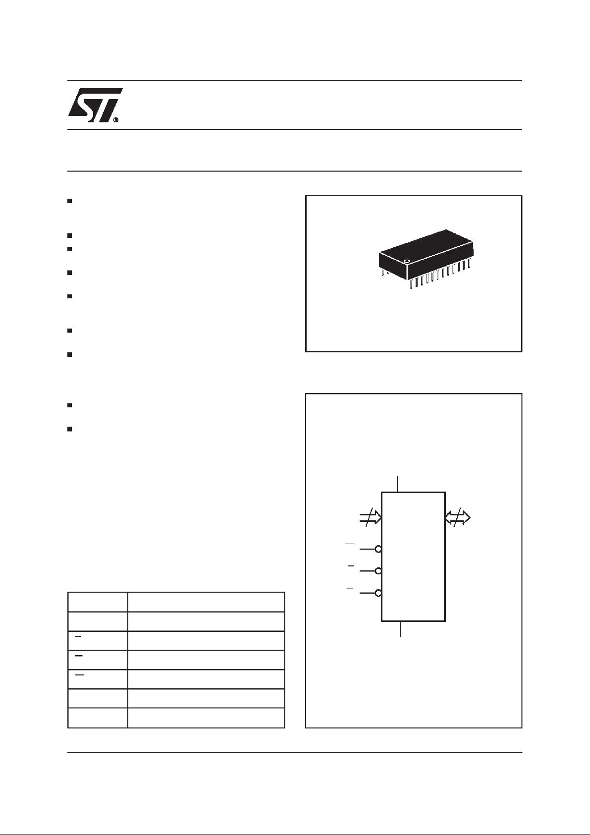
PCDIP24 (PC)
Battery/Crystal CAPHAT
Figure1. LogicDiagram
DESCRIPTION
TheM48T02/12TIMEKEEPER
RAMis a 2Kb x8
V
CC
non-volatile static RAM and real time clock which
is pin and functionalcompatiblewith theDS1642.
A special 24 pin 600mil DIP CAPHATpackage
11
A0-A10
8
DQ0-DQ7
housesthe M48T02/12siliconwith a quartzcrystal
and a long life lithium button cell to form a highly
integratedbatterybacked-upmemoryandrealtime
clocksolution.
W
M48T02
M48T12
E
Table1. SignalNames
G
A0-A10 Address Inputs
DQ0-DQ7 Data Inputs / Outputs
E Chip Enable
G Output Enable
W Write Enable
V
CC
V
SS
November 1998 1/15
Supply Voltage
Ground
V
SS
AI01027
M48T02, M48T12
Table2. AbsoluteMaximum Ratings
(1)
Symbol Parameter Value Unit
T
A
T
STG
(2)
T
SLD
V
IO
V
CC
I
O
P
D
Notes: 1. Stresses greater than those listed under ”AbsoluteMaximum Ratings” may cause permanent damage to the device. This is a
stress rating only and functional operation of thedevice at these or any other conditionsabove those indicated in the operational
section of this specification is notimplied.Exposure to theabsolute maximum rating conditions for extended periods of timemay
affect reliability.
2. Soldering temperature not to exceed 260°C for 10 seconds (total thermal budget not to exceed 150°C for longer than 30 seconds).
CAUTION:
Ambient Operating Temperature 0 to 70 °C
Storage Temperature (VCCOff, Oscillator Off) –40 to 85
Lead SolderTemperaturefor 10 seconds 260 °C
Input or Output Voltages –0.3to 7 V
Supply Voltage –0.3to 7 V
Output Current 20 mA
Power Dissipation 1 W
Negativeundershoots below –0.3 volts are not allowed on any pin while inthe Battery Back-up mode.
C
°
Table3. OperatingModes
Mode V
CC
Deselect
Write V
Read V
4.75V to 5.5V
or
4.5V to 5.5V
Read V
to V
Deselect V
SO
Deselect
Notes:X=VIHor VIL;VSO= Battery Back-upSwitchover Voltage.
(min) X X X High Z CMOS Standby
PFD
V
≤
SO
E G W DQ0-DQ7 Power
V
IH
IL
IL
IL
X X High Z Standby
XVILD
V
IL
V
IH
V
IH
V
IH
High Z Active
IN
D
OUT
Active
Active
X X X High Z BatteryBack-up Mode
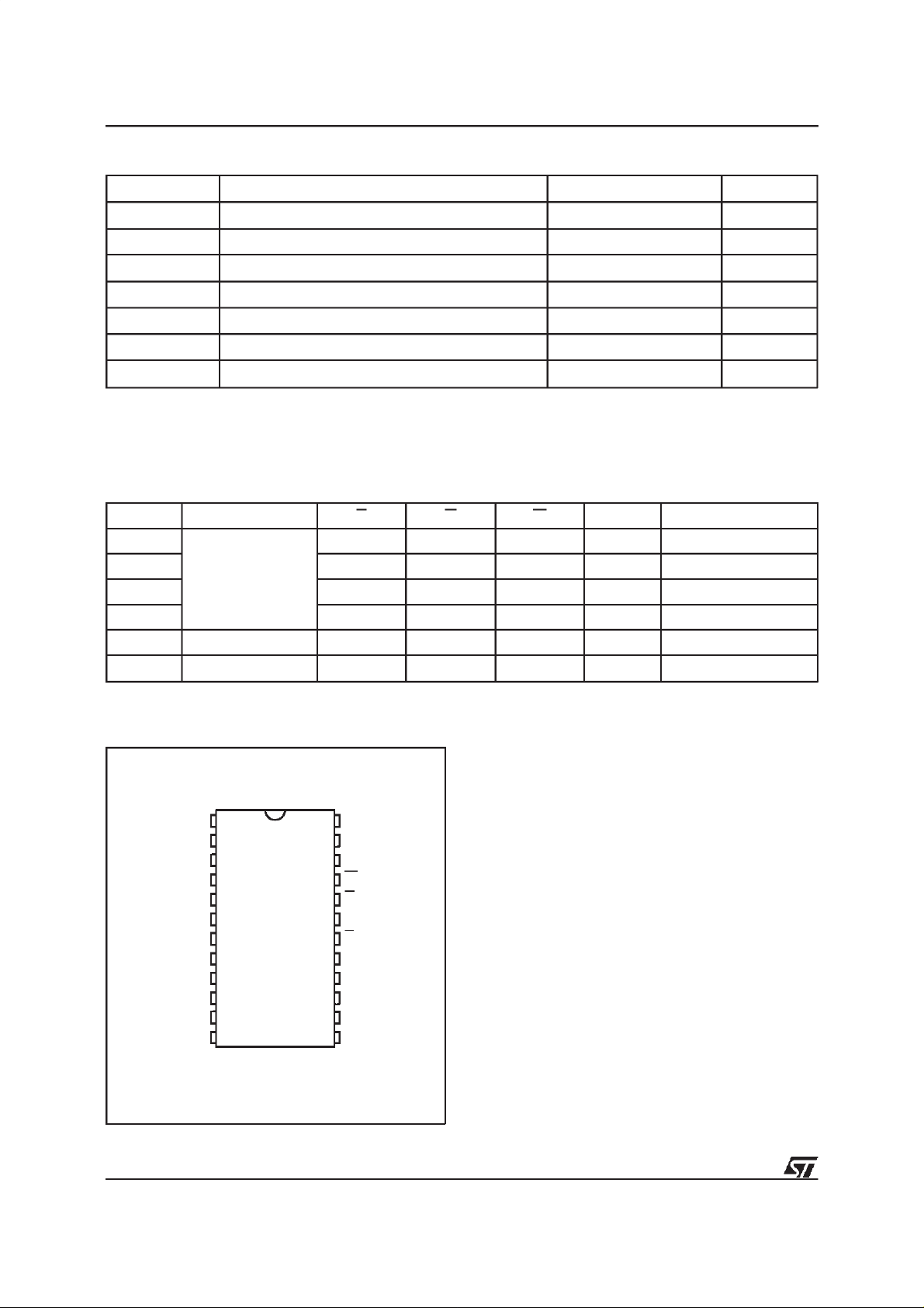
Figure2. DIPPin Connections
A7
2/15
A6
A5
A4
A3
A2
A1
A0
DQ0
DQ2
SS
1
2
3
4
5
6
7
8
9
10
11
12
M48T02
M48T12
24
23
22
21
20
19
18
17
16
15
14
13
AI01028
V
CC
A8
A9
W
G
A10
E
DQ7
DQ6
DQ5DQ1
DQ4
DQ3V
DESCRIPTION(cont’d)
The M48T02/12 button cell has sufficient capacity
andstoragelifetomaintaindataandclockfunctionality for an accumulatedtime period of at least 10
years in the absence of power over the operating
temperaturerange.
The M48T02/12is a non-volatilepin and function
equivalentto any JEDECstandard 2Kb x8 SRAM.
It also easily fits into many ROM, EPROM, and
EEPROM sockets, providing the non-volatility of
PROMs without any requirement for special write
timing or limitations on the number of writes that
canbe performed.
AsFigure3shows,thestaticmemoryarrayandthe
quartzcontrolledclockoscillatorof the M48T02/12
areintegratedon one silicon chip. The two circuits
are interconnectedat the upper eight memory locations to provide user accessible BYTEWIDE
clockinformationinthebyteswithaddresses7F8h7FFh.The clocklocationscontainthe year,month,
date,day,hour,minute,andsecondin24hourBCD
format.Corrections for 28,29 (leap year), 30, and
31 day months are made automatically.
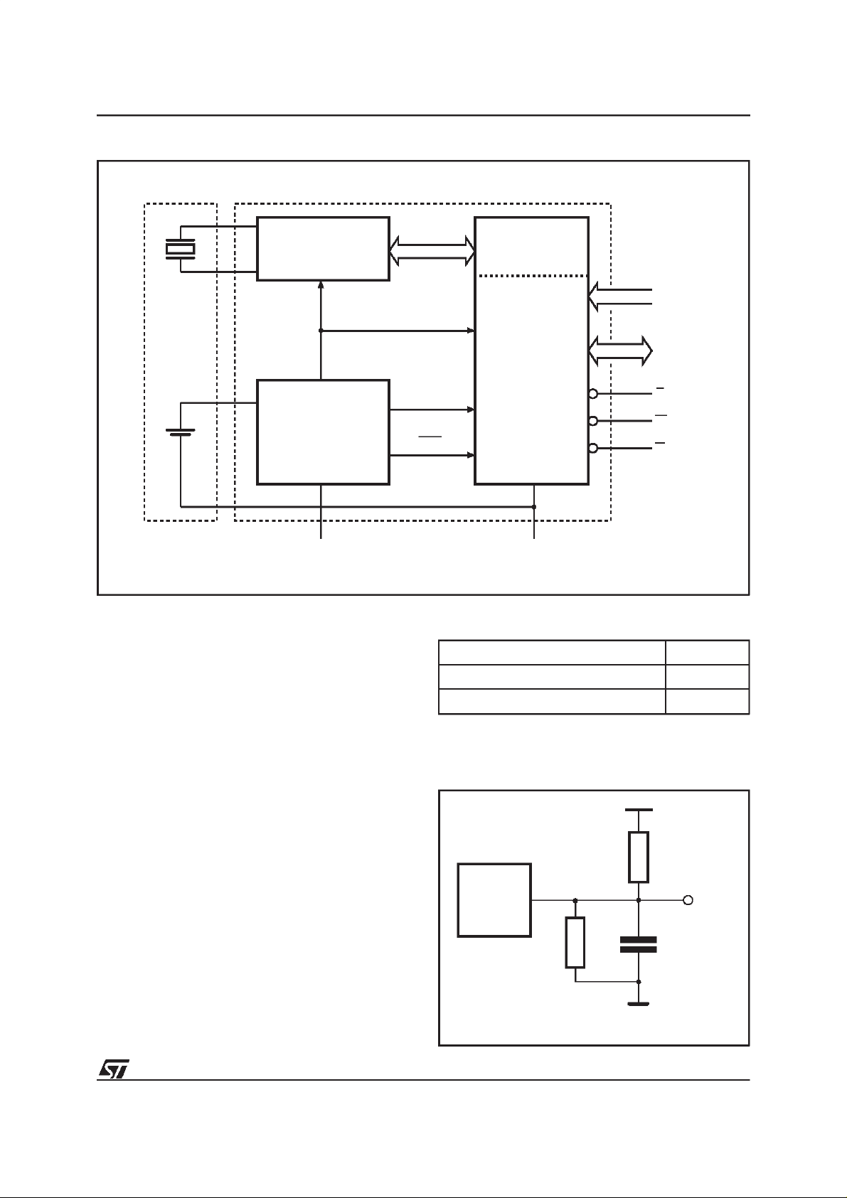
Figure3. Block Diagram
M48T02, M48T12
OSCILLATOR AND
CLOCK CHAIN
32,768
Hz
CRYSTAL
POWER
LITHIUM
CELL
VOLTAGE SENSE
AND
SWITCHING
CIRCUITRY
V
CC
Byte 7F8h is the clock control register. This byte
controlsuser access to the clock information and
also stores the clock calibrationsetting.
The eight clock bytes are not the actual clock
counters themselves; they are memory locations
consisting of BiPORTread/write memory cells.
The M48T02/12 includes a clock control circuit
whichupdatestheclockbyteswithcurrentinformation once per second. The information can be
accessedby the user in the same manner as any
other location in the staticmemory array.
TheM48T02/12also hasits ownPower-failDetect
circuit.Thecontrolcircuitryconstantlymonitorsthe
single 5V supply for an out of tolerancecondition.
When V
is out of tolerance, the circuit write
CC
protectstheSRAM,providingahighdegreeof data
security in the midst of unpredictablesystem operation brought on by low V
.AsVCCfalls below
CC
approximately3V,the controlcircuitryconnectsthe
battery which maintains data and clock operation
until valid powerreturns.
8 x 8 BiPORT
SRAM ARRAY
A0-A10
DQ0-DQ7
E
W
G
V
PFD
BOK
2040 x
SRAM ARRAY
8
V
SS
Table4. AC MeasurementConditions
Input Rise and Fall Times
Input Pulse Voltages 0V to 3V
Input and Output TimingRef. Voltages 1.5V
Note that OutputHi-Z is defined as the point where data is no
longer driven.
Figure4. AC TestingLoad Circuit
5V
1.8kΩ
DEVICE
UNDER
TEST
1kΩ
AI01329
5ns
≤
OUT
CL= 100pF
CLincludes JIG capacitance
AI01019
3/15
M48T02, M48T12
Table5. Capacitance
(1)
(TA=25°C, f = 1 MHz )
Symbol Parameter Test Condition Min Max Unit
C
IN
(2)
C
IO
Notes: 1. Effective capacitance measured with power supply at 5V.
2. Outputs deselected.
Input Capacitance VIN=0V 10 pF
Input / Output Capacitance V
=0V 10 pF
OUT
Table6. DC Characteristics
=0 to 70°C; VCC=4.75V to 5.5V or 4.5Vto 5.5V)
(T
A
Symbol Parameter Test Condition Min Max Unit
(1)
I
LI
(1)
I
LO
I
CC
I
CC1
I
CC2
(3)
V
IL
V
IH
V
OL
V
OH
Notes: 1. Outputs Deselected.
2. Measured with Control Bitsset as follows: R = ’1’;W, ST,KS, FT = ’0’.
Input Leakage Current 0V ≤ VIN≤ V
Output Leakage Current 0V ≤ V
OUT
≤ V
CC
CC
Supply Current Outputs open 80 mA
(2)
Supply Current (Standby) TTL E = V
(2)
Supply Current (Standby) CMOS E = VCC– 0.2V 3 mA
IH
Input Low Voltage –0.3 0.8 V
Input High Voltage 2.2 VCC+ 0.3 V
Output Low Voltage IOL= 2.1mA 0.4 V
Output High Voltage IOH= –1mA 2.4 V
±1 µA
±5 µA
3mA
Table7. PowerDown/Up Trip Points DC Characteristics
(1)
(TA=0 to 70°C)
Symbol Parameter Min Typ Max Unit
V
PFD
V
PFD
V
SO
t
DR
Notes: 1. All voltagesreferenced to VSS.
2. At 25°C.
4/15
Power-fail Deselect Voltage (M48T02) 4.5 4.6 4.75 V
Power-fail Deselect Voltage (M48T12) 4.2 4.3 4.5 V
Battery Back-up Switchover Voltage 3.0 V
(2)
Expected Data Retention Time 10 YEARS
M48T02, M48T12
Table8. PowerDown/Up Mode AC Characteristics
=0 to 70°C)
(T
A
Symbol Parameter Min Max Unit
t
PD
(1)
t
F
(2)
t
FB
t
R
t
RB
t
REC
Notes:1.V
2. V
V
E or W at VIHbefore Power Down 0
V
(max) to V
PFD
V
(min) to VSOVCCFall Time 10
PFD
V
(min) to V
PFD
VSOto V
PFD
(min) VCCFall Time 300 µs
PFD
(max) VCCRise Time 0 µs
PFD
(min) VCCRise Time 1
E or W at VIHafter PowerUp 2 ms
(max) to V
PFD
passes V
CC
(min) to VSOfall timeof less than tFBmay cause corruption of RAMdata.
PFD
(min) fall timeof less thantFmay result in deselection/write protection not occurring until 50 µs after
PFD
(min).
PFD
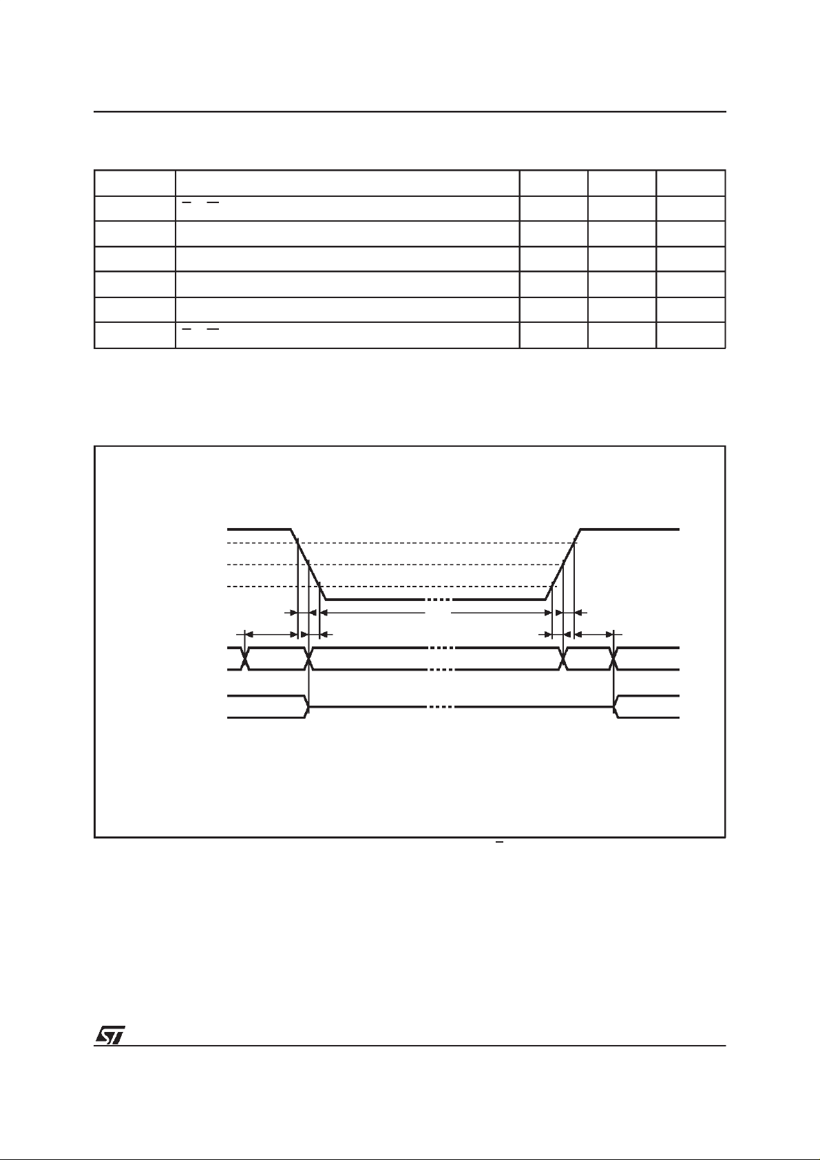
Figure5. Power Down/UpMode AC Waveforms
V
CC
V
(max)
PFD
V
(min)
PFD
V
SO
tF
tFB
INPUTS
tDR
DON’T CARE
NOTE
s
µ
s
µ
s
µ
tR
tRECtPD tRB
RECOGNIZEDRECOGNIZED
OUTPUTS
Note:
Inputs may or may not berecognizedat this time. Caution should betakento keep E high as V
may perform inadvertent write cycles after V
reset is being applied to the processor, a reset conditionmay not occur until after the system clock is running.
VALID VALID
(PER CONTROL INPUT)
rises above V
CC
(min) but before normal system operations begin. Eventhough a power on
PFD
HIGH-Z
rises past V
CC
(PER CONTROL INPUT)
AI00606
(min). Some systems
PFD
5/15

M48T02, M48T12
Table9. Read Mode AC Characteristics
(T
=0 to 70°C; VCC=4.75V to 5.5V or 4.5Vto 5.5V)
A
Symbol Parameter
M48T02 / M48T12
-70 -150 -200
Min Max Min Max Min Max
Unit
t
AVAV
t
AVQV
t
ELQV
t
GLQV
t
ELQX
t
GLQX
t
EHQZ
t
GHQZ
t
AXQX
Read Cycle Time 70 150 200 ns
Address Validto Output Valid 70 150 200 ns
Chip Enable Low to Output Valid 70 150 200 ns
Output Enable Low to Output Valid 35 75 80 ns
Chip Enable Low to OutputTransition 5 10 10 ns
Output Enable Low to OutputTransition 5 5 5 ns
Chip Enable High to OutputHi-Z 25 35 40 ns
Output Enable High to OutputHi-Z 25 35 40 ns
Address Transitionto Output Transition 10 5 5 ns
Figure6. Read Mode AC Waveforms
A0-A10
tAVQV tAXQX
tELQV
tAVAV
VALID
tEHQZ
E
G
DQ0-DQ7
Note: Write Enable (W) = High.
6/15
tELQX
tGLQX
tGLQV
tGHQZ
VALID
AI01330

Table10. Write ModeAC Characteristics
(T
=0 to 70°C; VCC=4.75V to 5.5V or 4.5Vto 5.5V)
A
Symbol Parameter
M48T02, M48T12
M48T02 / M48T12
-70 -150 -200
Min Max Min Max Min Max
Unit
t
AVAV
t
AVWL
t
AVEL
t
WLWH
t
ELEH
t
WHAX
t
EHAX
t
DVWH
t
DVEH
t
WHDX
t
EHDX
t
WLQZ
t
AVWH
t
AVEH
t
WHQX
Write Cycle Time 70 150 200 ns
Address Validto Write Enable Low 0 0 0 ns
Address Validto Chip Enable Low 0 0 0 ns
Write Enable Pulse Width 50 90 120 ns
Chip Enable Low to ChipEnable High 55 90 120 ns
Write Enable High to Address Transition 0 10 10 ns
Chip Enable High to Address Transition 0 10 10 ns
Input Valid to Write Enable High 30 40 60 ns
Input Valid to Chip Enable High 30 40 60 ns
Write Enable High to Input Transition 5 5 5 ns
Chip Enable High to Input Transition 5 5 5 ns
Write Enable Low to Output Hi-Z 25 50 60 ns
Address Validto Write Enable High 60 120 140 ns
Address Validto Chip Enable High 60 120 140 ns
Write Enable High to Output Transition 5 10 10 ns
READMODE
The M48T02/12 is in theRead Mode wheneverW
(Write Enable) is high and E (Chip Enable) is low.
The device architecture allows ripple-through access of data from eight of 16,384 locations in the
static storage array. Thus, the unique address
specified by the11 Address Inputs defines which
one of the 2,048 bytes of data is to be accessed.
Valid data will be available at the Data I/O pins
within Address Access time (t
) after the last
AVQV
addressinput signalis stable,providing thatthe E
andG accesstimes are also satisfied.If the E and
G access times are not met, valid data will be
availableafterthe latterof theChipEnableAccess
time (t
) orOutputEnable Accesstime (t
ELQV
GLQV
The state of theeight three-state Data I/O signals
iscontrolledbyEand G. Iftheoutputsare activated
before t
indeterminate state until t
, the data lines will be driven to an
AVQV
. If the Address In-
AVQV
puts are changed while E and G remain active,
output data will remain valid for OutputData Hold
time(t
) butwill goindeterminateuntil the next
AXQX
AddressAccess.
WRITEMODE
The M48T02/12 is in the Write Mode wheneverW
and E are active.Thestart of a write is referenced
from the latter occurring falling edge of W or E.A
write is terminated by the earlier rising edge of W
orE. The addressesmustbeheld validthroughout
the cycle. E or W must return high for a minimum
of t
from Chip Enable or t
EHAX
WHAX
Enablepriortothe initiationof anotherreador write
cycle. Data-in mustbe validt
).
of write and remain valid for t
priorto the end
DVWH
WHDX
shouldbekepthighduringwritecyclesto avoidbus
contention; although, if the output bus has been
activated by a low on E and G, a low on W will
disablethe outputst
after W falls.
WLQZ
from Write
afterward. G
7/15

M48T02, M48T12
Figure7. WriteEnableControlled, WriteAC Waveforms
A0-A10
tAVEL
E
tAVWL
W
tWLQZ
DQ0-DQ7
tAVAV
VALID
tAVWH
tWLWH
Figure8. Chip Enable Controlled, Write AC Waveforms
tDVWH
tWHAX
tWHQX
tWHDX
DATA INPUT
AI01331
8/15
A0-A10
E
W
DQ0-DQ7
tAVEL
tAVWL
tAVAV
VALID
tAVEH
tELEH
DATA INPUT
tDVEH
tEHAX
tEHDX
AI01332B

M48T02, M48T12
DATARETENTIONMODE
WithvalidV
applied,theM48T02/12operatesas
CC
aconventionalBYTEWIDEstaticRAM.Shouldthe
supply voltage decay, the RAM will automatically
power-faildeselect,writeprotectingitselfwhenV
falls within the V
(max), V
PFD
(min) window. All
PFD
CC
outputsbecomehighimpedance,andallinputsare
treatedas ”don’tcare.”
Note:
A power failure during a write cycle may
corrupt data at the currently addressed location,
but does not jeopardize the rest of the RAM’s
content.At voltagesbelowV
(min),the usercan
PFD
beassuredthe memorywill bein a write protected
state,providedthe V
falltime is not less than tF.
CC
The M48T02/12 may respond to transient noise
spikeson V
duringthetime thedevice is samplingV
that reach into the deselectwindow
CC
CC
. Therefore, decoupling of the power supply lines is recommended.
Thepower switchingcircuit connectsexternal V
tothe RAMand disconnectsthe battery when V
CC
CC
risesabove VSO.AsVCCrises,the batteryvoltage
is checked. If the voltage is too low, an internal
BatteryNotOK (BOK) flagwillbeset.TheBOKflag
can be checkedafter power up. If the BOKflag is
set, the first write attempted will be blocked. The
flagisautomaticallyclearedafterthefirstwrite,and
normal RAM operation resumes. Figure 9 illustrates how a BOK check routine could be structured.
For more information on a Battery Storage Life
referto the ApplicationNote AN1012.
Figure9. Checking the BOK Flag Status
POWER-UP
READ DATA
AT ANYADDRESS
WRITE DATA
COMPLEMENT BACK
TO SAMEADDRESS
READ DATA
AT SAME
ADDRESS AGAIN
COMPLEMENT
OFFIRST
(BATTERY OK)
WRITE
DATA BACK TO
SAME ADDRESS
CONTINUE
ISDATA
READ?
YES
ORIGINAL
NO
(BATTERY LOW)
NOTIFY SYSTEM
OF LOW BATTERY
(DATA MAY BE
CORRUPTED)
CLOCKOPERATIONS
Readingthe Clock
Updatesto the TIMEKEEPERregistersshould be
haltedbeforeclockdata is read topreventreading
data in transition. Because the BiPORT TIMEKEEPER cells in the RAM array are only data
registers,andnot the actualclock counters,updating the registers can be halted without disturbing
the clock itself.
Updatingishaltedwhena ’1’iswrittentotheREAD
bit, the seventh bit in the control register. As long
asa ’1’remains inthatposition,updating is halted.
Aftera halt is issued,the registersreflectthecount;
thatis, the day,date,and the timethatwerecurrent
at the moment the halt commandwas issued.
All of the TIMEKEEPER registersare updated simultaneously.Ahalt will not interruptan update in
progress.Updatingis withinasecondafter theread
bit is reset to a ’0’.
AI00607
Settingthe Clock
The eighth bit of the control register is theWRITE
bit.Settingthe WRITEbit toa ’1’,liketheREADbit,
halts updatesto the TIMEKEEPERregisters. The
usercan thenloadthem withthe correctday,date,
and time data in 24 hour BCD format (see Table
10). Resettingthe WRITEbit toa’0’then transfers
the values of all time registers(7F9h-7FFh)to the
actual TIMEKEEPERcounters and allows normal
operationto resume.TheFTbitandthebitsmarked
as ’0’ in Table10 must be written to ’0’to allow for
normalTIMEKEEPERand RAM operation.
See the Application Note AN923 ”TIMEKEEPER
rolling into the 21st century” for more information
on Century Rollover.
9/15

M48T02, M48T12
Stoppingand Starting the Oscillator
The oscillator may be stoppedat any time. If the
device is going to spend a significant amount of
timeon the shelf,the oscillatorcan be turned off to
minimize current drain on the battery. The STOP
bit is the MSB of the secondsregister.Setting it to
a’1’stopstheoscillator.TheM48T02/12is shipped
fromSTMicroelectronicswith the STOPbit settoa
’1’. When reset to a ’0’, the M48T02/12 oscillator
startswithin 1 second.
Calibratingthe Clock
The M48T02/12 is driven by a quartz controlled
oscillatorwith a nominalfrequencyof 32,768Hz. A
typicalM48T02/12is accuratewithin ±1minuteper
monthat 25°C withoutcalibration.The devicesare
tested not to exceed±35 ppm (parts per million)
oscillator frequency error at 25°C, which equates
toabout ± 1.53minutes permonth. The oscillation
rate of any crystal changes with temperature(see
Figure10).Mostclockchipscompensateforcrystal
frequencyandtemperatureshifterrorwithcumbersome trim capacitors. The M48T02/12 design,
however,employsperiodiccountercorrection.The
calibrationcircuitaddsorsubtractscountsfromthe
oscillatordividercircuit at the divide by 256 stage,
asshown in Figure11.The numberof timespulses
are blanked (subtracted, negative calibration) or
split(added,positivecalibration)dependsuponthe
valueloadedinto the fivebit Calibrationbyte found
in the ControlRegister. Adding countsspeeds the
clockup, subtractingcounts slowstheclockdown.
The Calibration byte occupies the five lower order
bits in the Control register.This byte can be set to
represent any value between 0 and 31 in binary
form.The sixth bit isa signbit; ’1’indicatespositive
calibration, ’0’ indicates negative calibration. Calibrationoccurswithin a 64 minutecycle. Thefirst62
minutes in the cycle may, once per minute, have
onesecond either shortenedor lengthenedby 128
oscillator cycles. If a binary ’1’ is loaded into the
register, only the first 2 minutes in the 64 minute
cycle will be modified; if a binary 6 is loaded, the
first12 will be affected,and soon.
Therefore, each calibration step has the effect of
addingorsubtracting256oscillatorcyclesforevery
125,829,120actualoscillatorcycles,that is+4.068
or–2.034ppm ofadjustmentpercalibrationstepin
thecalibrationregister.Assumingthatthe oscillator
isin factrunning at exactly32,768 Hz, each of the
31 increments in the Calibrationbyte would represent +10.7 or –5.35 seconds per month which
corresponds to a total range of +5.5 or –2.75
minutesper month.
Two methods are available for ascertaining how
muchcalibration a given M48T02/12 may require.
The first involvessimply setting the clock, letting it
run for a month and comparing it to a known
accurate reference (like WWV broadcasts).While
thatmay seemcrude,it allowsthe designerto give
theend userthe abilityto calibratehis clockashis
environmentmayrequire,evenafter thefinalproduct is packaged in a non-user serviceable enclosure.All the designer has to do is providea simple
utilitythat accessesthe Calibrationbyte.
Table11. Register Map
Address
D7 D6 D5 D4 D3 D2 D1 D0
7FFh 10 Years Year Year 00-99
7FEh 0 0 0 10 M. Month Month 01-12
7FDh 0 0 10 Date Date Date 01-31
7FCh 0 FT 0 0 0 Day Day 01-07
7FBh 0 0 10 Hours Hours Hour 00-23
7FAh 0 10 Minutes Minutes Minutes 00-59
7F9h ST 10 Seconds Seconds Seconds 00-59
7F8h W R S Calibration Control
Keys: S = SIGN Bit
FT = FREQUENCY TEST Bit (Set to ’0’ for normal clock operation)
R = READBit
W = WRITE Bit
ST = STOPBit
0 = Must be set to ’0’
10/15
Data
Function/Range
BCD Format

Figure10. CrystalAccuracy Across Temperature
M48T02, M48T12
ppm
20
0
-20
-40
-60
-80
-100
0 5 10 15 20 25 30 35 40 45 50 55 60 65 70
Figure11. Clock Calibration
∆F
= -0.038 (T - T
F
ppm
C
T0=25°C
)2± 10%
0
2
°C
AI02124
NORMAL
POSITIVE
CALIBRATION
NEGATIVE
CALIBRATION
AI00594B
11/15

M48T02, M48T12
CLOCKOPERATION
(cont’d)
The second approach is better suited to a manufacturing environment, and involves the use of
some test equipment. When the Frequency Test
(FT)bit, the seventh-mostsignificantbit in the Day
Register, issetto a ’1’,andthe oscillatorisrunning
at32,768 Hz,the LSB (DQ0)of the SecondsRegister will toggle at 512 Hz.Any deviation from512
Hz indicates the degree and direction of oscillator
frequencyshift at thetest temperature.For example, a reading of 512.01024Hz would indicate a
+20 ppm oscillator frequency error, requiring a
-10(WR001010)to be loaded into the Calibration
Byte for correction. Note that settingor changing
theCalibrationByte does notaffect the Frequency
testoutputfrequency.The devicemustbe selected
and address 7F9h must be held constant when
readingthe 512 Hz on DQ0.
TheFTbitmustbeset usingthesamemethodused
toset theclock,usingthe Write bit. TheLSB ofthe
Seconds Register is monitored by holding the
M48T02/12 in an extended read of the Seconds
Register, without having the Read bit set. The FT
bitMUSTbe resetto ’0’for normalclockoperations
to resume.
Formore information oncalibration,see the ApplicationNote AN924 ”TIMEKEEPERCalibration”.
whichstabilizesthe V
bus.The energystored in
CC
thebypasscapacitorswillbe releasedas lowgoing
spikes are generated or energy will be absorbed
when overshoots occur.A bypasscapacitor value
of0.1µF (as shown in Figure12) is recommended
in order to providethe needed filtering.
Inaddition to transientsthat are causedby normal
SRAM operation, power cycling can generate
negative voltage spikes on V
values below V
by as muchas one Volt.These
SS
that drive it to
CC
negative spikes can cause data corruption in the
SRAM while in battery backup mode. To protect
from these voltage spikes, it is recommeded to
connecta schottkydiodefrom V
connected to V
, anode to VSS). Schottky diode
CC
toVSS(cathode
CC
1N5817 is recommended for through hole and
MBRS120T3is recommendedfor surfacemount.
Figure12. SupplyVoltageProtection
V
CC
V
CC
0.1µF DEVICE
POWER SUPPLY DECOUPLING and UNDERSHOOTPROTECTION
transients,includingthoseproducedby output
I
CC
switching,canproducevoltagefluctuations,resultingin spikes on the V
bus. Thesetransientscan
CC
be reduced if capacitorsare used to store energy,
V
SS
AI02169
12/15

ORDERINGINFORMATION SCHEME
Example: M48T02 -70 PC 1
M48T02, M48T12
Supply Voltageand Write
Speed
Package
Temp. Range
ProtectVoltage
02 V
12 V
= 4.75V to 5.5V
CC
V
= 4.5V to 4.75V
PFD
= 4.5V to 5.5V
CC
V
= 4.2V to 4.5V
PFD
-70 70ns
-150 150ns
-200 200ns
PC PCDIP24
1 0to 70 °C
Fora listofavailableoptions(Speed,Package,etc...)orforfurtherinformationonany aspect ofthis device,
pleasecontact the STMicroelectronicsSales Officenearest to you.
13/15

M48T02, M48T12
PCDIP24 - 24 pin Plastic DIP, battery CAPHAT
Symb
Typ Min Max Typ Min Max
A 8.89 9.65 0.350 0.380
A1 0.38 0.76 0.015 0.030
A2 8.38 8.89 0.330 0.350
B 0.38 0.53 0.015 0.021
B1 1.14 1.78 0.045 0.070
C 0.20 0.31 0.008 0.012
D 34.29 34.80 1.350 1.370
E 17.83 18.34 0.702 0.722
e1 2.29 2.79 0.090 0.110
e3 25.15 30.73 0.990 1.210
eA 15.24 16.00 0.600 0.630
L 3.05 3.81 0.120 0.150
N24 24
mm inches
Drawing is not to scale.
14/15
B1 B e1
e3
D
N
1
A2A1A
E
L
C
eA
PCDIP

M48T02, M48T12
Information furnished is believed to be accurate and reliable. However, STMicroelectronics assumes no responsibility for the consequences
ofuse ofsuch information nor for any infringementof patents or otherrights of third parties which may result from its use. No license is granted
by implicationor otherwise underanypatent or patent rights ofSTMicroelectronics. Specificationsmentioned in thispublication are subject to
change without notice. This publication supersedes and replaces all information previously supplied. STMicroelectronics products are not
authorized for use as criticalcomponents in lifesupport devices or systems without express written approval of STMicroelectronics.
The ST logo is a registered trademark of STMicroelectronics
1998 STMicroelectronics - All Rights Reserved
TIMEKEEPER is a registeredtrademark ofSTMicroelectronics
CAPHAT,BYTEWIDE and BiPORTare trademarks of STMicroelectronics
Australia - Brazil - Canada- China - France - Germany - Italy - Japan - Korea - Malaysia - Malta - Mexico - Morocco - The Netherlands -
Singapore - Spain - Sweden- Switzerland - Taiwan - Thailand - United Kingdom- U.S.A.
STMicroelectronics GROUP OF COMPANIES
http://www.st.com
15/15
 Loading...