

Page 1
查询M440T1MV供应商
3.3V, 32 Mbit (1024 Kbit x 32) TIMEKEEPER® SRAM
FEAT URES SUMMARY
■ 3.3V ± 10%
■ INTEGRATED ULTRA LOW POWER SRAM,
REAL TIME CLOCK, POWER-FAIL
CONTROL CIRCUIT, BATTERY, AND
CRYSTAL
■ PRECISION POWER MONITORING AND
POWER SWITCHING CIRCUITRY
■ AUTOMATIC WRITE - PR OTEC TION WHEN
IS OUT-OF-TOLE R A NC E
V
CC
■ POWER-FAIL DESELECT VOLTAGE:
–V
■ BATTERY LOW PIN (BL)
■ DUAL BATTERY SNAPHAT
= 3.0 to 3.6V; 2.8V ≤ V
CC
REPLACEABLE
■ 85ns SRAM CHIP ENABLE ACCESS (70ns
ADDRESS ACCESS)
■ SLEEP MODE FUNCTION
■ 150ns CLOCK ACCESS
≤ 2.97V
PFD
®
HOUSING IS
M440T1MV
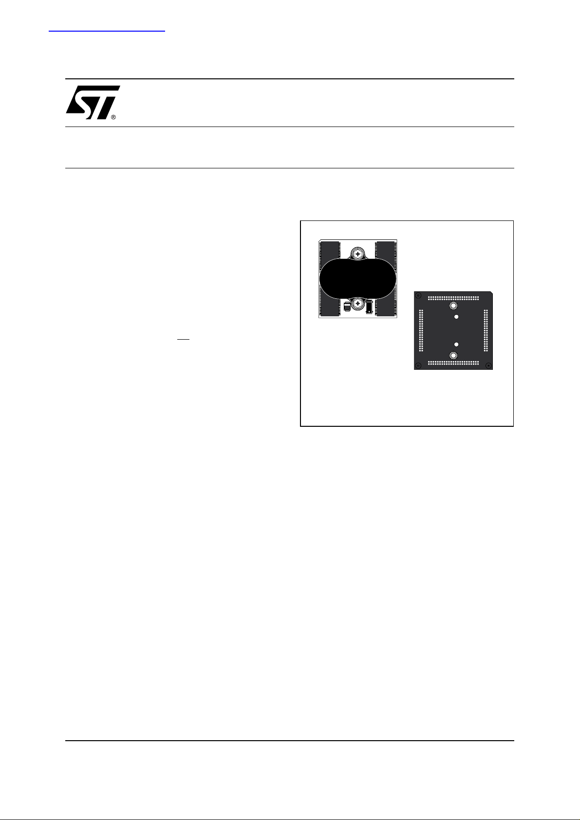
Figure 1. Package
M440T1MV
168-ball PBGA
Module
1/26October 2004
Page 2

M440T1MV
TABLE OF CONTENTS
FEATURES SUMMARY . . . . . . . . . . . . . . . . . . . . . . . . . . . . . . . . . . . . . . . . . . . . . . . . . . . . . . . . . . . . . 1
Figure 1. Package. . . . . . . . . . . . . . . . . . . . . . . . . . . . . . . . . . . . . . . . . . . . . . . . . . . . . . . . . . . . . . . 1
SUMMARY DESCRIPTION. . . . . . . . . . . . . . . . . . . . . . . . . . . . . . . . . . . . . . . . . . . . . . . . . . . . . . . . . . . 4
Figure 2. Logic Diagram . . . . . . . . . . . . . . . . . . . . . . . . . . . . . . . . . . . . . . . . . . . . . . . . . . . . . . . . . . 4
Table 1. Signal Names . . . . . . . . . . . . . . . . . . . . . . . . . . . . . . . . . . . . . . . . . . . . . . . . . . . . . . . . . . 4
Figure 3. PBGA Connections (Top View) . . . . . . . . . . . . . . . . . . . . . . . . . . . . . . . . . . . . . . . . . . . . . 5
Figure 4. M440T1MV Hardware Hookup . . . . . . . . . . . . . . . . . . . . . . . . . . . . . . . . . . . . . . . . . . . . . 6
Figure 5. M440T1MV PBGA Modul e Solution (Side/Top). . . . . . . . . . . . . . . . . . . . . . . . . . . . . . . . . 7
OPERATION MODES . . . . . . . . . . . . . . . . . . . . . . . . . . . . . . . . . . . . . . . . . . . . . . . . . . . . . . . . . . . . . . . 8
Memory READ Mode. . . . . . . . . . . . . . . . . . . . . . . . . . . . . . . . . . . . . . . . . . . . . . . . . . . . . . . . . . . . 8
Clock READ Mode. . . . . . . . . . . . . . . . . . . . . . . . . . . . . . . . . . . . . . . . . . . . . . . . . . . . . . . . . . . . . . 8
Table 2. Memory Operating Modes. . . . . . . . . . . . . . . . . . . . . . . . . . . . . . . . . . . . . . . . . . . . . . . . . 8
Table 3. Clock Operating Modes . . . . . . . . . . . . . . . . . . . . . . . . . . . . . . . . . . . . . . . . . . . . . . . . . . . 9
Figure 6. Memory READ Mode AC Waveforms, Chip Enable- or Output Enable-Con trolled. . . . . . 9
Figure 7. Memory READ Mode AC Waveforms, Address-Controlled. . . . . . . . . . . . . . . . . . . . . . . . 9
Figure 8. Clock READ Mode AC Waveforms, Chip Enable- or Output Enable-Controlled. . . . . . . 10
Figure 9. Clock READ Mode AC Waveforms, Address-Controlled. . . . . . . . . . . . . . . . . . . . . . . . . 10
Table 4. M em ory/Clock READ Mode AC Characteristics . . . . . . . . . . . . . . . . . . . . . . . . . . . . . . . 10
Memory WRITE Mode . . . . . . . . . . . . . . . . . . . . . . . . . . . . . . . . . . . . . . . . . . . . . . . . . . . . . . . . . . 11
Clock WRITE Mode . . . . . . . . . . . . . . . . . . . . . . . . . . . . . . . . . . . . . . . . . . . . . . . . . . . . . . . . . . . . 11
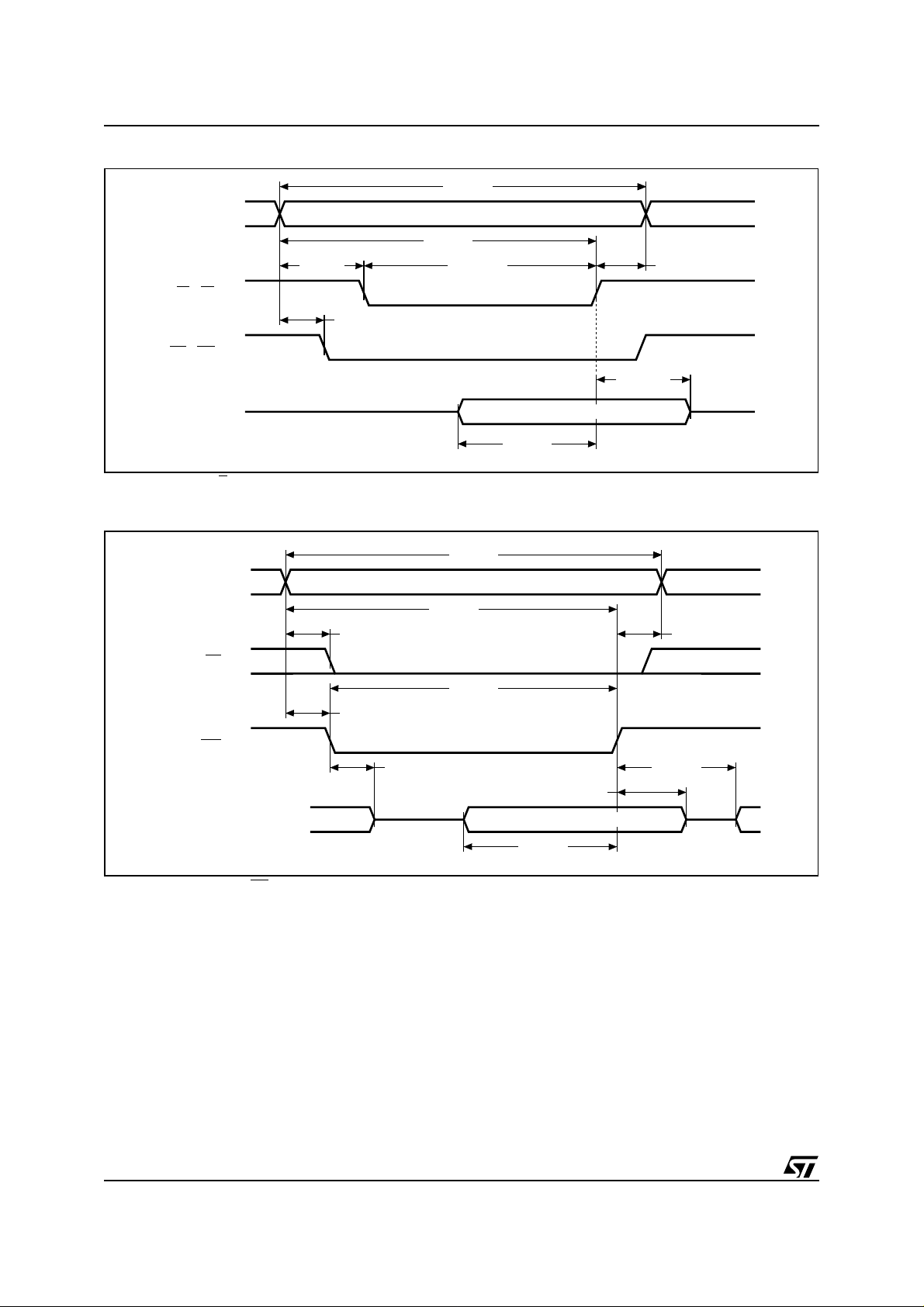
Figure 10.Memory WRITE Mode AC Waveforms, WRITE Enable-Controlled . . . . . . . . . . . . . . . . 11
Figure 11.Memory WRITE Mode AC Waveforms, Chip Enable-Controlled . . . . . . . . . . . . . . . . . . 12
Figure 12.Clock WRITE Mode AC Waveforms, WRITE Enable-Controlled . . . . . . . . . . . . . . . . . . 12
Figure 13.Clock WRITE Mode AC Waveforms, Chip Enable-Controlled. . . . . . . . . . . . . . . . . . . . . 13
Table 5. Memory/Clock WRITE Mode AC Characteristics . . . . . . . . . . . . . . . . . . . . . . . . . . . . . . 13
CLOCK OPERATION . . . . . . . . . . . . . . . . . . . . . . . . . . . . . . . . . . . . . . . . . . . . . . . . . . . . . . . . . . . . . . 14
Clock Registers . . . . . . . . . . . . . . . . . . . . . . . . . . . . . . . . . . . . . . . . . . . . . . . . . . . . . . . . . . . . . . . 14
Reading and Setting the Clock. . . . . . . . . . . . . . . . . . . . . . . . . . . . . . . . . . . . . . . . . . . . . . . . . . . 14
Clock Alarm Registers . . . . . . . . . . . . . . . . . . . . . . . . . . . . . . . . . . . . . . . . . . . . . . . . . . . . . . . . . 1 4
Watchdog Alarm Registers. . . . . . . . . . . . . . . . . . . . . . . . . . . . . . . . . . . . . . . . . . . . . . . . . . . . . . 14
Table 6. Register Map . . . . . . . . . . . . . . . . . . . . . . . . . . . . . . . . . . . . . . . . . . . . . . . . . . . . . . . . . . 1 5
Table 7. Time of Day Alarm Mask Bits . . . . . . . . . . . . . . . . . . . . . . . . . . . . . . . . . . . . . . . . . . . . .15
Command Register . . . . . . . . . . . . . . . . . . . . . . . . . . . . . . . . . . . . . . . . . . . . . . . . . . . . . . . . . . . . 16
Battery Low . . . . . . . . . . . . . . . . . . . . . . . . . . . . . . . . . . . . . . . . . . . . . . . . . . . . . . . . . . . . . . . . . . 1 6
Sleep Mode. . . . . . . . . . . . . . . . . . . . . . . . . . . . . . . . . . . . . . . . . . . . . . . . . . . . . . . . . . . . . . . . . . . 16
MAXIMUM RATINGS . . . . . . . . . . . . . . . . . . . . . . . . . . . . . . . . . . . . . . . . . . . . . . . . . . . . . . . . . . . . . . 17
Table 8. Absolute Maximum Ratings. . . . . . . . . . . . . . . . . . . . . . . . . . . . . . . . . . . . . . . . . . . . . . . 17
DC AND AC PARAMETERS. . . . . . . . . . . . . . . . . . . . . . . . . . . . . . . . . . . . . . . . . . . . . . . . . . . . . . . . . 18
2/26
Page 3

M440T1MV
Table 9. DC and A C Measurem ent Conditions . . . . . . . . . . . . . . . . . . . . . . . . . . . . . . . . . . . . . . . 18
Figure 14.AC Testing Load Circuit . . . . . . . . . . . . . . . . . . . . . . . . . . . . . . . . . . . . . . . . . . . . . . . . . 18
Table 10.Capacitance. . . . . . . . . . . . . . . . . . . . . . . . . . . . . . . . . . . . . . . . . . . . . . . . . . . . . . . . . . . 18
Table 11.DC Characteristics. . . . . . . . . . . . . . . . . . . . . . . . . . . . . . . . . . . . . . . . . . . . . . . . . . . . . . 1 9
Data Retention Mode. . . . . . . . . . . . . . . . . . . . . . . . . . . . . . . . . . . . . . . . . . . . . . . . . . . . . . . . . . . 2 0
Figure 15.Power Down/Up Mode AC Waveforms. . . . . . . . . . . . . . . . . . . . . . . . . . . . . . . . . . . . . . 20
Table 12.Power Down/Up Trip Points DC Characteristics . . . . . . . . . . . . . . . . . . . . . . . . . . . . . . . 20
Table 13.Power Down/Up AC Characteristics . . . . . . . . . . . . . . . . . . . . . . . . . . . . . . . . . . . . . . . . 21
PACKAGE MECHANICAL INFORMATION . . . . . . . . . . . . . . . . . . . . . . . . . . . . . . . . . . . . . . . . . . . . . 22
Figure 16.PBGA-ZA – 168-ball Plastic Ball Grid Array Package Outline . . . . . . . . . . . . . . . . . . . .22
Table 14. PBGA-ZA – 168-ball Plastic Ball Grid Array Package Mechanical Data . . . . . . . . . . . . . 23
PART NUMBERING . . . . . . . . . . . . . . . . . . . . . . . . . . . . . . . . . . . . . . . . . . . . . . . . . . . . . . . . . . . . . . . 24
Table 15.Ordering Information Scheme . . . . . . . . . . . . . . . . . . . . . . . . . . . . . . . . . . . . . . . . . . . . . 24
REVISION HISTORY . . . . . . . . . . . . . . . . . . . . . . . . . . . . . . . . . . . . . . . . . . . . . . . . . . . . . . . . . . . . . . . 25
Table 16.Document Revision History. . . . . . . . . . . . . . . . . . . . . . . . . . . . . . . . . . . . . . . . . . . . . . . 25
3/26
Page 4
M440T1MV
SUMMARY DESCRIPTION
The M440T1MV TIMEKEEPER® RAM i s a 16M bit ,
non-volatile static RAM organized as 1,024K by 32
bits and real time clock org anized as 64 bytes by
8 bits. The special PBGA package provides a fully
integrated battery back-up memory and real tim e
clock so lution. I n the e vent of powe r instab ility o r
absence, a self-contained battery maintains the
timekeeping operation and provides power for a
CMOS static RAM. Control circuitry monitors V
CC
and invokes write protection to prevent data corruption in the memory and RTC.
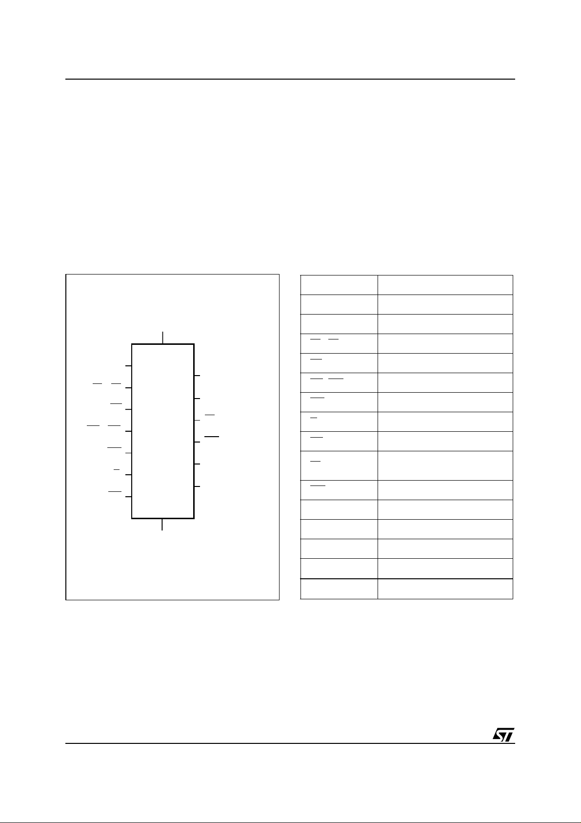
Figure 2. Logic Diagram Table 1. Signal Names
The clock keeps track of tenths/hundredths of seconds, seconds, minutes , hou rs, day, date, month,
and year information. The last day of the month is
automatically adjusted for months with less than
31 days, including leap year correction.
The clock operates in one of two formats:
– a 12-hour mode with an AM/PM indicator; or
– a 24-hour mode
The M440T1MV is in a 168-ball PBGA module that
integrates the RTC, the battery, and SRAM in one
package.
A0 - A19 Address Inputs
DQ0 - DQ31 NVRAM Data Input/Outp ut
A0 – A19
E1 – E4
EC
W1 – W4
WC
GC
G
V
CC
M440T1MV
V
SS
DQ0 – DQ31
DQC0 – DQC7
BL
IRQ
RSV1
RSV2
AI04200
DQC0 - DQC7 Clock Data Input/Output
- E4 NVRAM Chip Enable Inputs
E1
EC
- W4 NVRAM WRITE Enable Inputs
W1
WC
G
GC
BL
IRQ
RSV1 Reserved
RSV2 Reserved
NC No Connect
V
CC
V
SS
Clock Chip Enable Input
Clock WRITE Enable Input
Output Enable Input
Clock Output Enable Input
Battery Low Output (Open
Drain)
Interrupt Output (Open Drain)
Supply Voltage
Ground
4/26
Page 5
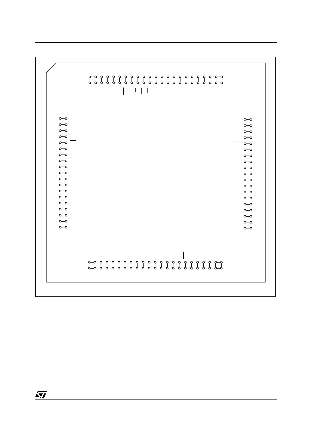
Figure 3. PBGA Connections (Top View)
M440T1MV
10
12
13
14
15
16
17
18
19
11
79
787776
80
E1
BL
CC
V
1
A15
2
3
4
5
6
7
8
9
A17
A13
A18
W1
A16
A14
A12
A7
A6
A5
DQ7
DQ6
DQ5
A19
DQ4
DQ0
DQ1
DQ2
EC
74
727170
73
75
G
WC
W2
E2
GC
M440T1MV
E4
696867
A11
A10
A8
666564
A0
A9
W4
63
A1
A2A3A4
626160
V
CC
E3
DQ31
DQ30
DQ29
W3
DQ28
DQ27
DQ24
DQ25
DQ26
DQ16
DQ17
DQ18
DQ23
RSV1
DQ22
DQ21
DQ20
DQ19
59
58
57
56
55
54
53
52
51
50
49
48
47
46
45
44
43
42
41
SS
V
DQC3
DQC4
DQC5
23
24
RSV2
25
DQC7
DQC6
26
27
DQC0
DQC1
29
28
DQ3
21
22
20
Note: This diagra m is T OP VIEW perspective (vie w through package).
DQC2
DQ10
31
30
DQ9
32
DQ8
33
DQ15
35
34
IRQ
DQ14
36
DQ13
DQ12
37
38
V
DQ11
39
40
SS
AI04794
5/26
Page 6

M440T1MV
Figure 4. M440T1MV Hardware Hookup
M48T224W
3.3V
V
CC
6
A0-A5
E
DQ0 - DQ7 DQC0 - DQC7
W
INTB/INTB
G
E1
E2
E3
E4
SLEEP
THS
V
SS
SLEEP
PAD
EC
WC
GC
E1
E2
E3
E4
8k
Ω
V
OUTA
V
OUTA
E1
CON
E2
CON
BL BL
V
OUTB
E3
CON
E4
CON
IRQ
V
E
V
E
20
CC
1M x 8
20
CC
1M x 8
SRAM
A0-A19
SRAM
G
G
A0-A19
G
DQ0-DQ7
8
W
W1
DQ16-DQ23
8
W
W3
V
E
E
V
E
20
CC
CC
A0-A19
1M x 8
SRAM
G
G
A0-A19
20
1M x 8
SRAM
G
GG
DQ8-DQ15
8
W
W2
DQ24-DQ31
8
W
W4
AI04795
6/26
Page 7
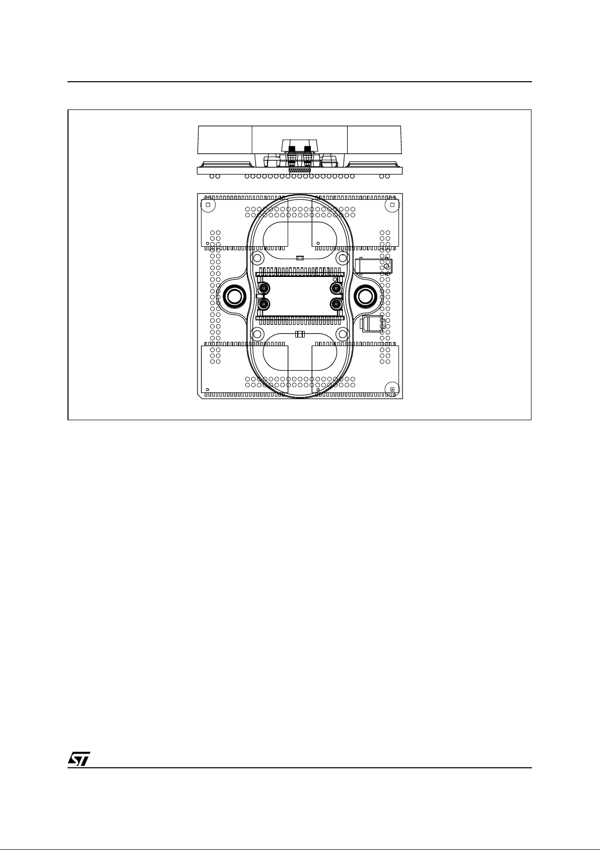
Figure 5. M4 40 T1MV PBGA Mo dule Solution ( S id e/Top)
M440T1MV
AI04628b
7/26
Page 8
M440T1MV
OPERATION MODES
Memory READ Mode
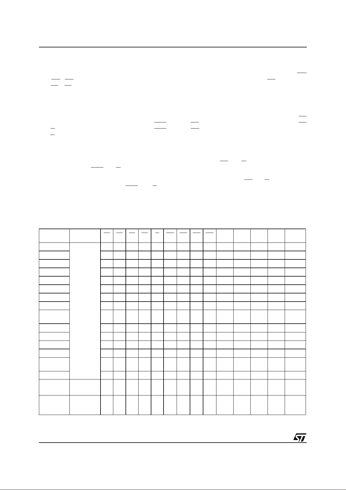
The M440T1MV is in the 32-bit READ Mode whenever W1
and E1
(see Table 2., page 8). The uniq ue address specified by the 20 address inputs defines which one of
the 1,048,576 long words of data is to be accessed. Valid data will be available at the Data I/O pins
within Address Access Time (t
address input signal is st able, providing the E 1-4
and G access times are also satisfied. If the E1-4
and G access times are not met, valid data will be
available after the latter of the Chip Enable Access
Times (t
(t
The state of the thirty-two three-state Data I/O signals is controlled by E1-4
activated before t
to an indeterminate state until t
dress Inputs are changed while E1-4
main active, output data will remain valid for
Output Data Hold Time (t
minate until the next Address Access.
- W4 (WRITE Enable Byte 1 to 4) are high
- E4 - Chip Enable Bytes 1 to 4 are low
) after the last
AVQV
) or Output Enable Access Time
ELQV
).
GLQV
and G. If the outputs are
, the data lines will be driven
AVQV
AVQV
) but will go indeter-
AXQX
. If the Ad-
and G re-
Clock READ Mode
The clock is in the READ Mode whenever WC
(Clock WRITE Enable) is high and EC (Clock Chip
Enable) is low. The unique address specified by
the 6 Address Inputs defines wh ich one of the 64
bytes of clock data is to be accessed. Valid data
will be available at the Data I/O pins (DQC0-7)
within Address Access Time (t
) after the last
AVQV
address input signal is stable, providing the EC
and GC access times are also satisfied. If the EC
and GC access times are not met, valid data will
be available after the latter of the Chip Enable Access Times (t
).
(t
GLQV
) or Output Enable Access Time
ELQV
The state of the eight t hree-state Da ta I/O si gnals
is contr olled by E C
vated before t
an indeterminate state until t
Inputs are changed while EC
and G. If the outputs are acti-
, the data lines will be driven to
AVQV
. If the Address
AVQV
and G remain active,
output dat a will re main valid for Ou tput D ata H old
Time (t
) but will go indeterminate until the
AXQX
next Address Access. See section on Reading and
Setting the Clock under CLO CK OPER ATION for
more details.
Table 2. Memory Operating Modes
DQ24-
Mode
Byte WRITE
Byte WRITE H H L H H X X L X Hi-Z Hi-Z
Byte WRITE H L H H H X L X X Hi-Z
Byte WRITE LHHHHL X XX
Byte WRITE X X X L H H H H L Hi-Z Hi-Z Hi-Z
Byte WRITE X X L X H H H L H Hi-Z Hi-Z
Byte WRITE X L X X H H L H H Hi-Z
Byte WRITE L X X X H L H H H
Long Word
WRITE
Byte READ H H H L L X X X H Hi-Z Hi-Z Hi-Z
Byte READ H H L H L X X H X Hi-Z Hi-Z
Byte READ H L H H L X H X X Hi-Z
Byte READ L H H H L H X X X
Long Word
READ
Deselect H H H H X X X X X Hi-Z Hi-Z Hi-Z Hi-Z Stdby
Deselect
Deselect
Note: X = VIH or VIL; VSO = Battery B ack-up Switchover Voltage.
1. See Table 12., page 20 for details.
V
CC
2.97 to 3.6V
VSO to
(min)
V
PFD
(1)
≤ V
SO
E4 E3 E2 E1 G W4 W3 W2 W1
H H H L H X X X L Hi-Z Hi-Z Hi-Z
LLLLHLLLL
LLLLLHHHH
X X X X X X X X X Hi-Z Hi-Z Hi-Z Hi-Z
(1)
X X X X X X X X X Hi-Z Hi-Z Hi-Z Hi-Z
DQ16-
DQ31
DQ23
D
IN
D
IN
D
IN
D
OUT
D
OUTDOUTDOUTDOUT
DQ8-
DQ0-
DQ15
D
IN
D
Hi-Z Hi-Z Active
IN
Hi-Z Hi-Z Hi-Z Active
D
IN
D
Hi-Z Hi-Z Active
IN
Hi-Z Hi-Z Hi-Z Active
D
D
IN
D
OUT
Hi-Z Hi-Z Hi-Z Active
IN
D
D
OUT
Hi-Z Hi-Z Active
Power
DQ7
D
Active
IN
Hi-Z Active
D
Active
IN
Hi-Z Active
D
Active
IN
Active
OUT
Hi-Z Active
Active
CMOS
Standby
Battery
Back-up
Mode
8/26
Page 9
M440T1MV
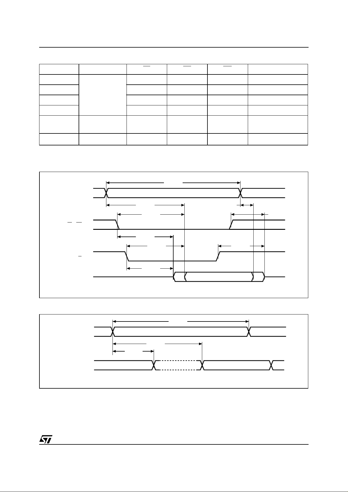
Table 3. Clock Operating Modes
Mode
Deselect
WRITE
READ
READ
Deselect
Deselect
Note: X = VIH or VIL; VSO = Battery B ack-up Switchover Voltage.
1. See Table 12., page 20 for details.
Figure 6. Memory READ Mode AC Waveforms, Chip Enable- or Output Enable-Controlled
V
CC
2.97 to 3.6V
VSO to
(min)
V
PFD
(1)
≤ V
SO
(1)
EC GC WC DQC0 - 7
V
IH
V
IL
V
IL
V
IL
X X Hi-Z
X
V
IL
V
IH
V
IL
V
IH
V
IH
D
D
Hi-Z
IN
OUT
X X X Hi-Z
X X X Hi-Z
tAVAV
A0-A19
tAVQV tAXQX
tELQV
E1 - E4
tELQX
G
tGLQX
DQ0-DQ31
VALID
tGLQV
DATA OUT
Figure 7. Memory READ Mode AC Waveforms, Address-Controlled
tAVAV
A0-A19
tAVQV
tAXQX
VALID
tEHQZ
tGHQZ
AI05606
DQ0-DQ31
DATA VALID
DATA VALID
AI05607
9/26
Page 10
M440T1MV
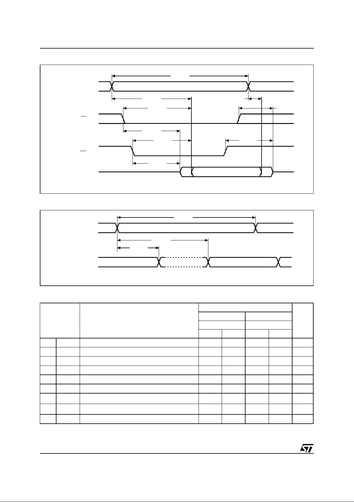
Figure 8. Clock READ Mode AC Waveforms, Chip Enable- or Output Enable-Controlled
tAVAV
A0-A5
tAVQV tAXQX
tELQV
EC
tELQX
GC
tGLQX
DQC0-DQC7
VALID
tGLQV
Figure 9. Clock READ Mode AC Waveforms, Address-Controlled
tAVAV
A0-A5
tAVQV
tAXQX
VALID
tEHQZ
tGHQZ
DATA OUT
AI04653
DQC0-DQC7
DATA VALID
DATA VALID
Table 4. Memory/Clock READ Mode AC Characteristics
M440T1MV
Symbol
t
RCtAVAV
t
ACCtAVQV
t
COtELQV
t
OEtGLQV
t
CELtELQX
t
OELtGLQX
t
CEZ t
EHQZ
t
OEZ t
GHQZ
t
OHtAXQX
Note: 1. Vali d fo r Ambient Operating Temperature: TA = –15 to 75°C; VCC = 3.0 to 3. 6V (excep t where not e d).
2. C
L
READ Cycle Time 85 150 ns
Address Valid to Output Valid 70 150 ns
Chip Enable Low to Output Valid 85 150 ns
Output Enable Low to Output Valid 45 70 ns
Chip Enable Low to Output Transition 5 10 ns
Output Enable Low to Output Transition 5 5 ns
(2)
Chip Enable High to Output Hi-Z 40 50 ns
(2)
Output Enable High to Output Hi-Z 30 50 ns
Address Transition to Output Transition 5 5 ns
= 5pF.
Parameter
(1)
Memory Clock
–85 –15
Min Max Min Max
AI04654
Unit
10/26
Page 11
M440T1MV
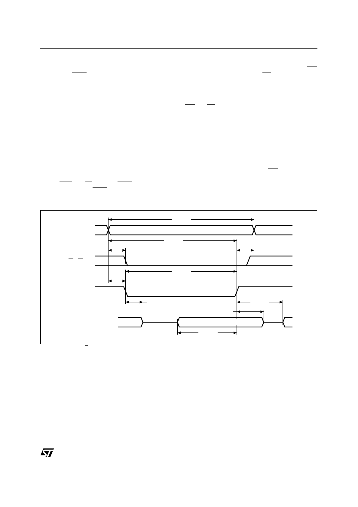
Memory WR I TE Mode
The M440T1MV is in the WRITE Mode whenever
any or all of W1-4
any corresponding E1-4
(WRITE Enable Byte 1 to 4) and
(Chip Enable Byte 1 to 4)
are in a low state after the address inputs are stable. Thus a Byte WRITE (8-bit), Word WRITE (16bit) or Long Word WRITE (32-bit) may be performed. The start of a WRITE is referenced from
the latter occurring falling edge of W1-4
or E1-4. A
WRITE is terminated by the earlier rising edge of
or E1-4. The addresses must be held valid
W1-4
throughout the cycle. E1-4
high for a mini mum of t
from WRITE Enable prior to the initiation of
t
WHAX
or W1-4 must return
from Chip En able or
EHAX
another READ or WRITE cycle. Data-in must be
valid t
valid for t
prior to the end of WRITE and remain
DVWH
afterward. G should be kept hi gh
WHDX
during WRITE cycles to avoid bus contention; although, if the output bus has been act ivated b y a
low on E1-4
outputs t
and G, a low on W1-4 will disable the
after W1-4 falls.
WLQZ
Clock WRITE Mode
The clock is in the WRITE Mode whenever WC
(Clock WRITE Enable) and EC (C lock Chip En able) are in the low state after the address inputs
are stable. The start of a WRITE is referenced
from the latter occurring falling edge of WC
A WRITE is terminated by the earlier rising edge of
or EC. The addresses must be held valid
WC
throughout the cycle. EC
for a minimum of t
from WRITE E nab le Clock prior to the initi-
t
WHAX
from Chip Enable Clock or
EHAX
ation of another READ or W RITE cycle. Data-in
must be valid t
remain valid for t
prior to the end of WRITE and
DVWH
afterward. GC shou ld be
WHDX
kept high during WRITE cycles to avoid bus contention; although, if the output bu s has be en activated by a low on EC
disable the outputs t
and GC a low on WC will
WLQZ
tion on Reading and Setting the Clock under
CLOCK OPERATION for more details.
Figure 10. Me m ory WRITE Mode AC Waveforms, WR I TE En abl e -C ontrolled
tAVAV
A0-A19
VALID
or EC.
or WC must return high
after WC falls. See sec-
E1 - E4
W1 - W4
DQ0-DQ31
Note: Output Enab l e (G ) = Low
tAVEL
tAVWL
tWLQZ
tAVWH
tWLWH
tDVWH
tWHAX
tWHQX
tWHDX
DATA INPUT
AI05608
11/26
Page 12
M440T1MV
Figu r e 1 1 . Memory WRIT E Mode AC W a vefor m s , Chip Enable - C ontro lled
tAVAV
A0-A19
tAVEL
E1 - E4
tAVWL
W1 - W4
DQ0-DQ31
Note: Output Enab l e (G ) = High
VALID
tAVEH
tELEH
DATA INPUT
tDVWH
Figure 12. Cl ock WR I TE Mode AC Wave fo rm s, W R IT E Ena bl e -C ontrolled
tAVAV
A0-A5
tAVEL
EC
VALID
tAVWH
tEHAX
tWHDX
AI05609
tWHAX
WC
DQC0-DQC7
Note: Clock Output Enable (GC) = Low
tAVWL
tWLQZ
tWLWH
tDVWH
tWHQX
tWHDX
DATA INPUT
AI04651
12/26
Page 13
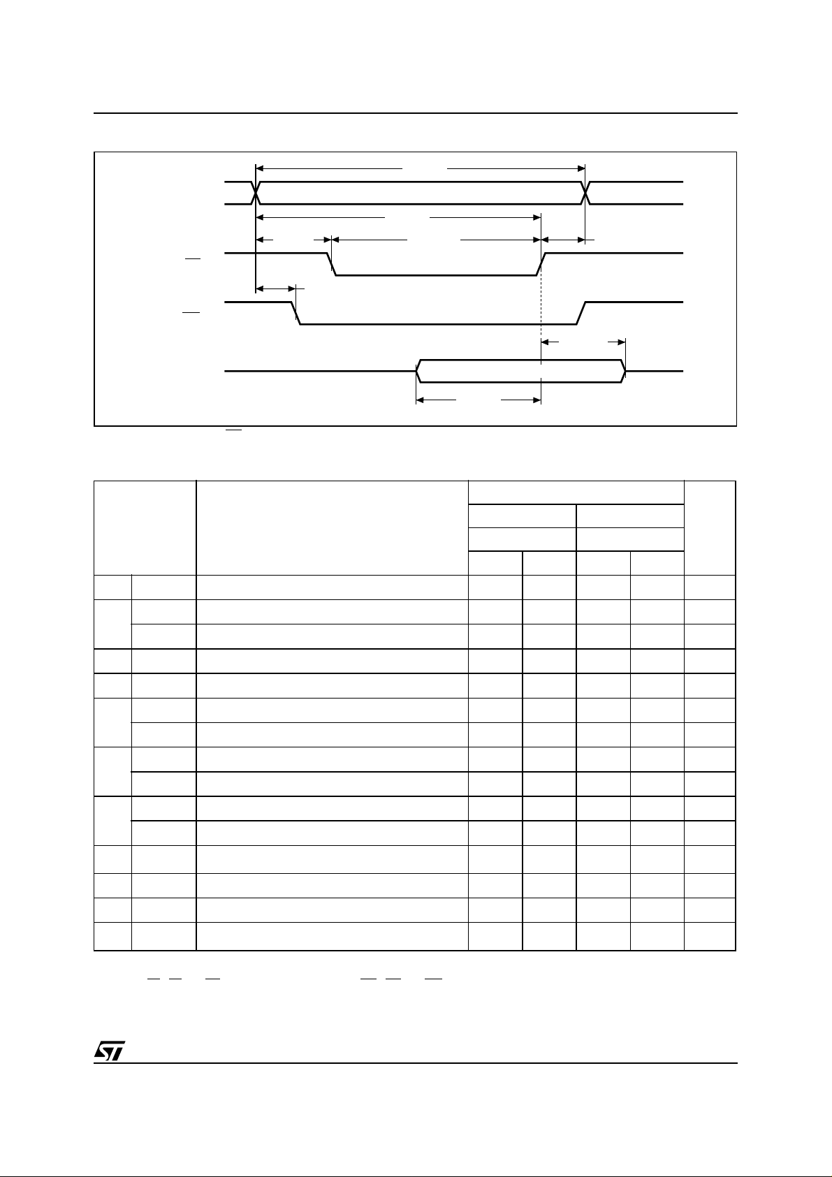
Figure 13. Clock WRITE Mode AC Waveforms, Chip Enable-Controlled
tAVAV
M440T1MV
A0-A5
tAVEL
EC
tAVWL
WC
DQC0-DQC7
Note: Clock Output Enable (GC) = High
VALID
tAVEH
tELEH
tWHDX
DATA INPUT
tDVWH
Table 5. Memory/Clock WRITE Mode AC Characteristics
M440T1MV
Symbol
t
WC
t
AW
t
WP
t
CEWtELEH
t
WR
t
DS
t
DH
t
WEZ t
t
OEW
Note: 1. Vali d fo r Ambient Operating Temperature: TA = –15 to 75°C; VCC = 3.0 to 3. 6V (excep t where not e d).
t
AVAV
t
AVWL
t
AVEL
t
WLWH
WRITE Cycle Time 85 150 ns
Address Valid to WRITE Enable Low 0 0 ns
Address Valid to Chip Enable Low 0 0 ns
WRITE Enable Pulse Width 60 100 ns
Chip Enable Low to Chip Enable High 65 150 ns
t
t
t
t
t
t
WLQZ
t
t
t
WHQX
2. C
L
3. If E1
WHAX
EHAX
DVWH
DVEH
WHDX
EHDX
AVWH
AVEH
= 5pF.
WRITE Enable High to Address Transition 0 10 ns
Chip Enable High to Address Transition 15 10 ns
Input Valid to WRITE Enable High 35 50 ns
Input Valid to Chip Enable High 35 50 ns
WRITE Enable High to Input Transition 0 0 ns
Chip Enable High to Input Transition 15 0 ns
(2,3)
WRITE Enable Low to Output Hi-Z 30 50 ns
Address Valid to WRITE Enable High 70 150 ns
Address Valid to Chip Enable High 70 150 ns
(3)
WRITE Enable High to Output Transition 5 5 ns
- E4 and EC goes low simultaneously with W1 - W4 and WC going low, the outp uts remain in the hi gh impedan ce state.
Parameter
(1)
Memory Clock
–85 –15
Min Max Min Max
tEHAX
AI04652
Unit
13/26
Page 14

M440T1MV
CLOCK OPERATION
Clock Registers
Registers 00h, 01h, 02h, 04h, 06h, 08h, 09h, and
0Ah contain the time of day data in BCD. Eleven
bits within these eight registers are not used and
will always read '0' regardless of how they are written. Bits 6 and 7 in the Mon ths Re gister (09h) are
binary bits. When set to logic '0,' EOSC
ables the R eal Time C lock oscilla tor. This b it will
normally be turned on by the user during device
initialization. However, the oscillator can be turned
on and off as necessary by set ting this bit to the
appropriate level. Bit 6 of the Hours Register is defined as the 12- or 24-hour select bit. When set to
logic '1,' the 12-hour format is select ed. In the 12hour format, Bit 5 is the AM/PM bit with logic '1' being PM. In the 24-hour mode, Bit 5 is the s econd
10-hour bit (20-23 hours). The Clock Registers are
updated every 0.01 seconds from the Real Time
Clock, except when the TE Bit (Bit 7 of Register
0Bh) is set low or the clock oscillator is not running.
Reading and Setting the Clock
The preferred method of synchronizing data access to and from the TIMEKEEPER
the Command Register by doing a WRITE cycle to
address location 0Bh and set ting TE B it (Tran sfer
Enable Bit) to a logic '0.' This will freeze the External Clock Registers at the present recorded time,
allowing access to occur without danger of simultaneous update. When the clock registers have
been read or written, a second WRITE cycle to location 0Bh and setting the TE Bit to a logic '1' will
put the Clock Registers back to being updated every 0.01 second. No time is lost in the Real Time
Clock because the internal copy of the Clock Register buffers is continually incremented while the
external memory registers are frozen. An alternate
method of reading and writing the Clock Registers
is to ignore synchronization. However, any single
READ may give erroneous data as t he Real Time
Clock may be in the process of updating the external memory registers as data is being read. The internal copies of seconds through years are
incremented, and the time of day alarm is checked
during the period that hundreds of seconds reads
“99” to “00.” A way of making sure data is valid is
to do multiple READs and compare. Writing the
registers can also produce erroneou s results for
the same reasons. A way of making sure that the
WRITE cycle has caused proper update is to do a
READ to verify and re-execute the WRITE cycle if
data is not correct. While the possibility of errone-
(Bit 7) en-
®
is to access
ous results from READ and WRITE cycles has
been stated, it is worth noting t hat the probability
of an incorrect result is kept to a minimu m due to
the redundant structure of the TIMEKEEPER.
Clock Alarm Registers
Registers 03h, 05h, and 07h contain the Clock
Alarm Registers. Bits 3, 4, 5, and 6 of Register 07h
will always read '0' regardless of how they are written. Bit 7 of Registers 03h, 05h, and 07h are mask
bits (see Table 6., page 15). When all of the mask
bits are logic '0,' a Clock Alarm will only occur
when Registers 02h, 04h, and 06h match the values stored in Registers 03h, 05h, and 07h. An
alarm will be generated every day when B it 7 of
Register 07h is set to a logic '1.' Similarly, an alarm
is generated every hour when Bit 7 of Registers
07h and 05h is set to a logic '1.' When Bit 7 of Registers 07h, 05h, and 03h is set to a logic '1,' an
alarm will occur every minute when Register 1
(seconds) rolls from “59” to “00.”
Clock Alarm Registers are written and read in the
same format as the Clock Registers. The Clock
Alarm Flag and Interrupt are always cleared when
alarm Registers are read or written.
Wat chdog Alarm Registers
Registers 0Ch and 0Dh contain the time for the
watchdog alarm. The two registers contain a time
count from 00.01 to 99.99 seconds i n BCD. The
value written into the Watchdog Alarm Reg isters
can be written or read in any order. Any access to
Register 0Ch or 0Dh will cause the watchdog
alarm to re-initialize and clears the Watchdog Flag
Bit and the Watchdog Interrupt Output. When a
new value is entered or the Watchdog Registers
are read, the watchdog timer will start counting
down from the entered value to zero. When zero is
reached, the Watchdog Interrupt Output will go to
the active state. The watchdog timer countdown is
interrupted and re-initialized back to the ent ered
value every time either of the registers are acc essed. In this manner, controlled periodic accesses to
the watchdog timer can prevent the watchdog
alarm from going to an active level. If access does
not occur, the countdown alarm will be repetitive.
The Watchdog Alarm Reg isters always read the
entered value. The actual countdown register is internal and is not readable. Writing registers 0Ch
and 0Dh to '0' will disable the watchdog alarm feature.
14/26
Page 15
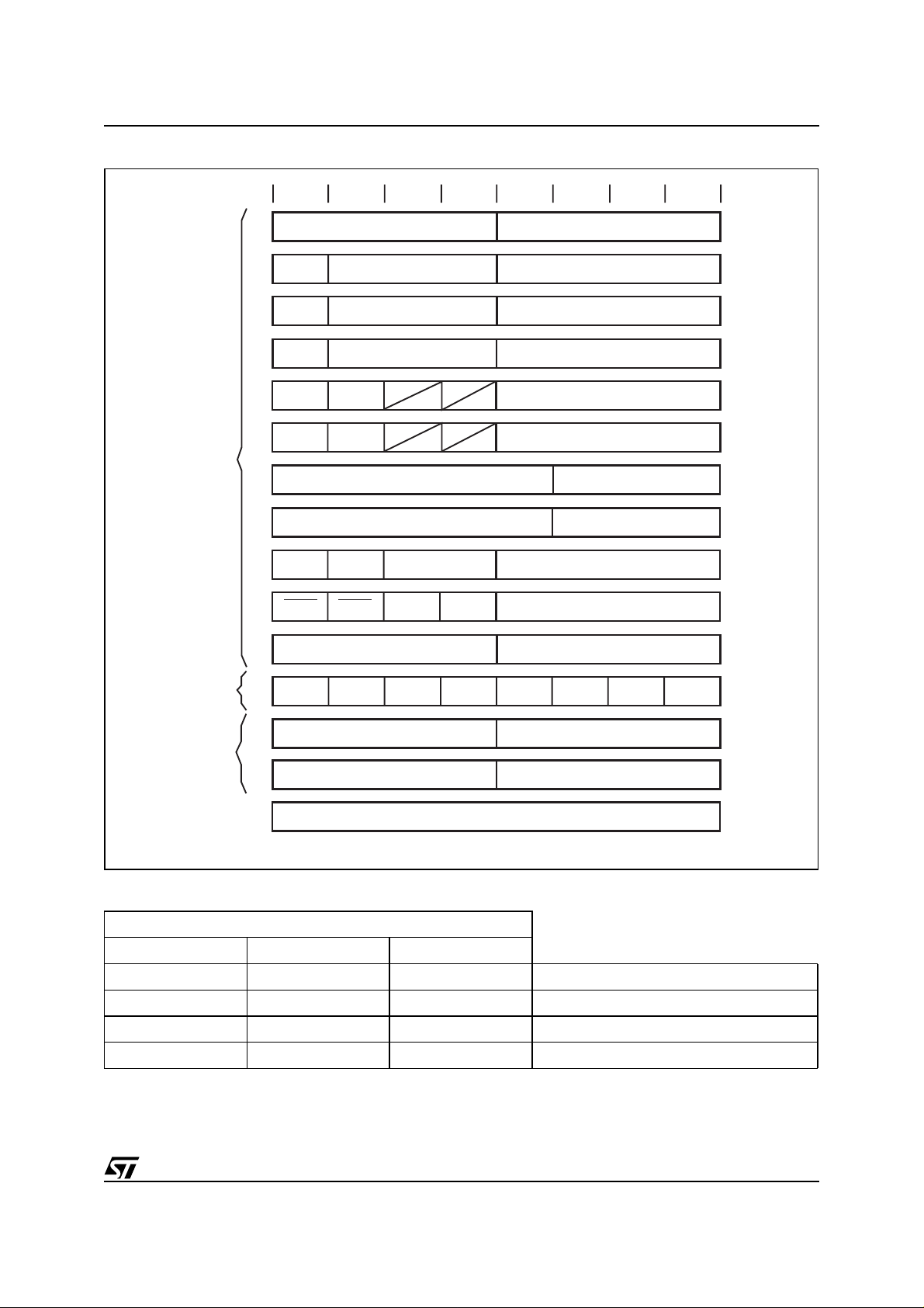
Table 6. Register Map
M440T1MV
CLOCK
CALENDAR/
TIME OF DAY
ALARM
REGISTERS
ADDRESS
BIT 7
0
1
0
2
0
3
M
0
4
5
M
0
6
7
M
8
0
9
EOSC
0.1 SECONDS
10 SECONDS
10 MINUTES
10 MIN ALARM
12/24
12/24
ESQW
10
10
0
0
0
A/P
A/P
0
0
10DATE
0
10
10
0
0
10MO
HR
HR
0.01 SECONDS
SECONDS
MINUTES
MIN ALARM
HOURS
HOURS ALARM
0
0
DAYS
DAY ALARM
DATE
MONTHS
BIT 0
RANGE
00-99
00-59
00-59
00-59
01-12+A/P
00-23
01-12+A/P
00-23
01-07
01-07
01-31
01-12
COMMAND
REGISTER
WATCHDOG
ALARM
REGISTERS
USER
REGISTERS
E - 3F
A
B
TE
C
D
10YEARS
IPSW
0.1 SECONDS
10 SECONDS
IBH
PU
LO
SRAM ADDRESS SPACE
LVL
WAM
Table 7. Time of Day Alarm Mask Bits
Register
(03h) Minutes (05h) Hours (07h) Days
1 1 1 Alarm once per minute
0 1 1 Alarm when minutes match
0 0 1 Alarm when hours and minutes match
0 0 0 Alarm when hours, minutes, and days match
Note: A ny other bit combinations of m ask bit setting s produce an illegal operation.
YEARS
TDM
0.01 SECONDS
WAF
SECONDS
00-99
TDF
00-99
00-99
AI04208
15/26
Page 16

M440T1MV
Command Register
Address location 0Bh is the Command Register
where mask bits, control bits, and fla g bits res ide.
The operation of each bit is as follows:
TE - Bit 7 Transfer Enable. This bit, when set to
logic '0,' will disable the transfer of data between
internal and external clock registers. The contents
in the external clock regi s ters are no w f roz en and
READs or WRITEs will not be affected with updates. This bit must be set to a logic '1' to allow updates.
IPSW - Bit 6 Interrupt Switch. When set to a
logic ' 1,' IRQ /(I R Q
set to a logic '0,' IRQ/(IRQ
output.
IBH/LO - Bit 5 IRQ
When this bit is set to a logic '1' and V
IRQ/(IRQ
) will source current (see Table
11., page 19, IOH). When this bit is set to a logic
'0,' IRQ will sink current (see Table 11., page 19,
).
I
OL
PU/LVL - Bit 4 Interrupt Pulse Mode or Level
Mode. This bit determines whether the interrupt
will output a pulse or level signal. When set to a
logic '0,' IRQ/( IRQ
this bit is set to a logic '1,' the pulse mode is selected. IRQ/(IRQ
pending on the condition of Bit 5, for a minimum of
3ms and then release. IRQ will only source current
when there is voltage present on V
WAM - Bit 3 Watchdog Alarm Mask. When this
bit is set to a logic '0,' the watchdog interrupt output
will be activated. The activated state is determined
by bits 1, 4, 5, and 6 of the Command Register.
when this bit is set to a logic '1 ,' the watchdog interrupt output is deactivated.
TDM - Bit 2 Time of Day Alarm Mask. When
this bit is set to a logic '0,' the ti me of day alarm interrupt output will be activated. The activated state
is determined by bits 0, 4, 5, and 6 o f the Command Register. When this bit is set to a logic '1,'
the time of day alarm interrupt output is deactivated.
WAF - Bit 1 Watchdog Alarm Flag. This bit is
set to a logic '1' when a wa tchdog alarm i nterrupt
occurs. This bit is “Read only.” The bit is reset
when any of the watchdog alarm reg isters are accessed.
When the interrupt is in the p ulse mode (see PU/
LVL - Bit 4 Interrupt Pulse Mode or Level Mode ),
this flag will be in the logic '1' state only during the
time the inter r u pt is active.
TDF - Bi t 0 Time of Day Flag. This is a “Read
only” bit. This bit is set to a logic '1' when a time of
day alarm has occurred. the time the alarm occurred can be determined by reading the time of
) is the Watch dog Al arm. When
) is the time of day alarm
Sink or Source Current.
is applied,
CC
) will be in the level mode. When
) will either sink or source current, de-
.
CC
day alarm registers. This bit is reset to a logic '0'
state when any of the time of day registers are accessed.
When the interrupt is in the p ulse mode (see PU/
LVL - Bit 4 Interrupt Pulse Mode or Level Mode ),
this flag will be in the logic '1' state only during the
time the inter r u pt is active.
Battery Low
The M440T1MV automatically performs battery
voltage monitoring upon power-up, and at factoryprogrammed time intervals of at least 24 hours.
The Battery Low (BL
) signal will b e asserted if t he
battery voltage is found to be less than approximately 2.5V. The BL
signal w ill remain asser ted
until completion of battery replacement and s ubsequent battery low monitoring tests, either during
the next power-up sequence or the next scheduled
24-hour interval (see application note, “AN1540,
NVRAM PBGA Dual Battery Hat Mounting and
Removal” for more information).
If a battery low is generated during a power-up sequence, this indicates that one of the batteries is
below 2.5V and may not be ab le to maintain data
integrity in the SRAM. Data should be considered
suspect, and verified as correct. Fresh batteries
should be installed.
If a battery low indication is generated during the
24-hour interval check, this indicates that the battery is near end o f life. However, data is not compromised due to the fact that a nominal V
CC
is
supplied. In order to insure data integrity during
subsequent periods of bat tery back-up m ode, the
batteries should be replaced. The SNAPHAT
should be replaced with valid V
applied to the
CC
®
top
device.
The M440T1MV only monitors the batteries when
a nominal V
is applied to the device. Thus appli-
CC
cations which require extensive durations in the
battery back-up mode should be powered-up periodically (at least once every few months) in order
for this technique to be beneficial. Additionally, if a
battery low is indicated, data integrity should be
verified upon power-up via a checksum or ot her
technique. The BL
signal is an open d rain output
and an appropriate pull-up resistor should be chosen to control the rise time.
Sleep Mode
Forcing the sleep p ad more positive than +7.5V
above ground will cause the batteries to be isolated from the RAM, preserving the remaining battery
life. This mode may be used when de vice operation is not necessary for an extended period of
time.
Note: Implementation of this Sleep Mode wi ll result in com ple t e lo s s of da ta .
16/26
Page 17
MAXIMUM RA T INGS
Stressing the device above the rating listed in the
“Absolute Maximum Ratings” table may cause
permanent damage to the device. These are
stress ratings only and operation of the device at
these or any other conditions above those indicated in the Operating sections of this specification is
Table 8. Absolute Maximum Ratings
Symbol Parameter Value Unit
not implied. Exposure to Absol ute Max imum Ra ting conditions for extended periods may affect device reliability. Refer also to the
STMicroelectronics SURE Program and other relevant quality documents.
M440T1MV
T
A
T
STG
T
SLD
V
CC
V
IO
I
O
P
D
CAUTION! Negative undershoots be l ow –0.3V are not al l owed on any pin while in the Bat tery Back-up M ode
Operating Temperature –15 to 75 °C
Storage Temperature (VCC, Oscillator Off)
Lead Solder Temperature for 10 seconds 260 °C
Supply Voltage (on any pin relative to Ground) –0.3 to + 4.6 V
Input or Output Voltages
Output Current 20 mA
Power Dissipation 1 W
–40 to 85 °C
–0.3 to V
CC
+ 0.3
V
17/26
Page 18
M440T1MV
DC AND AC PARAMETERS
This section summarizes the operating and measurement conditions, as well as the DC and AC
characteristics of the device. The parameters in
the following DC and AC Characteristic tables are
derived from tests performed under the Meas ure-
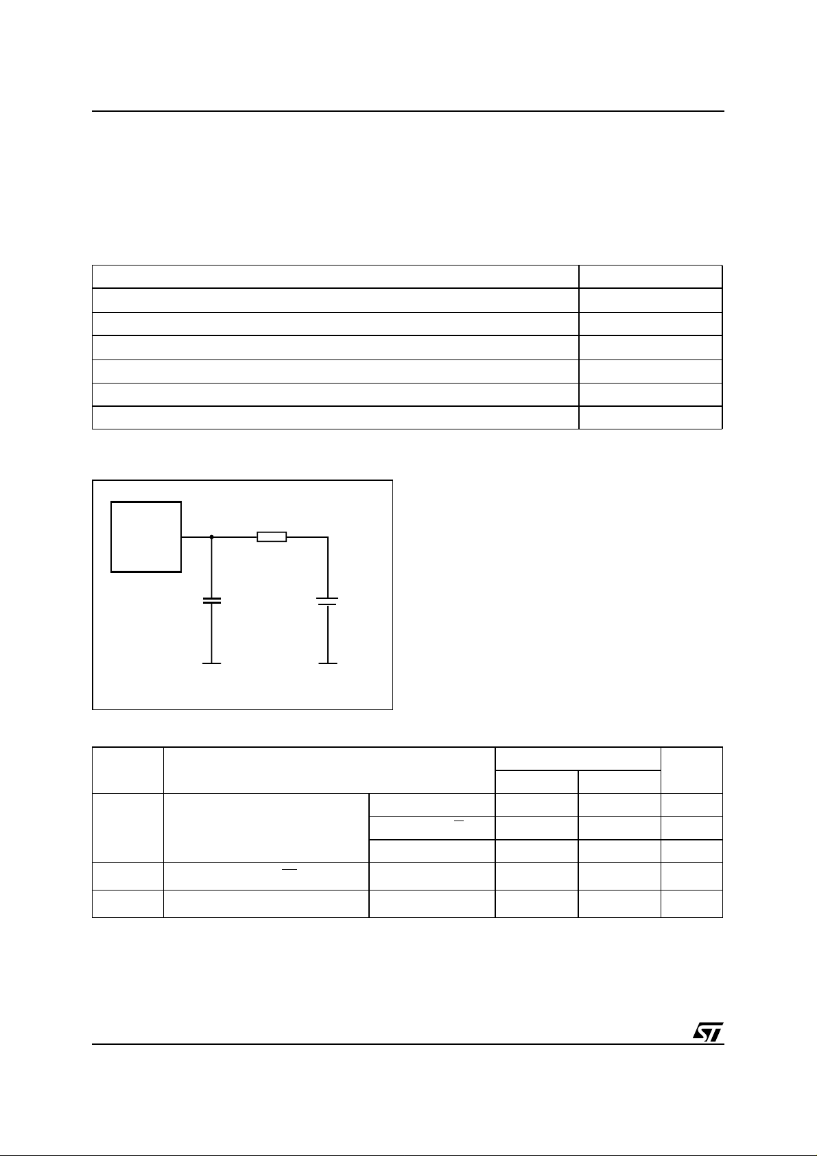
Table 9. DC and AC Measurement Conditions
Parameter M440T1MV
V
Supply Voltage
CC
Ambient Operating Temperature –15 to 75°C
Load Capacitance (C
Input Rise and Fall Times ≤ 5ns
Input Pulse Voltages 0 to 3V
Input and Output Timing Ref. Voltages 1.5V
Note: Output Hi-Z is defined as the p oi nt where data is no longer driven.
)
L
Figure 14. AC Testin g Load Cir cuit
ment Conditions listed in t he relevant tables. Designers should check that the operating conditions
in their projects match the measurement conditions when using the quoted parameters.
3.0 to 3.6V
30pF
DEVICE
645Ω
UNDER
TEST
CL = 30 pF
1.75V
AI05605
Table 10. Capacitance
Symbol
C
C
OUT
C
IO
Note: 1. Effective capacit ance measured with powe r supply at 3V; s am pl ed only; not 100% tested.
2. At 25°C, f = 1MHz.
3. Outputs were deselected.
Input Capacitance
IN
(3)
Output Capacitance (BL)10pF
(3)
Input / Output Capacitance 10 pF
Parameter
(1,2)
Min Max
A0 - A5 50 pF
A6 - A19, G 40 pF
All Other Inputs 10 pF
M440T1MV
Unit
18/26
Page 19
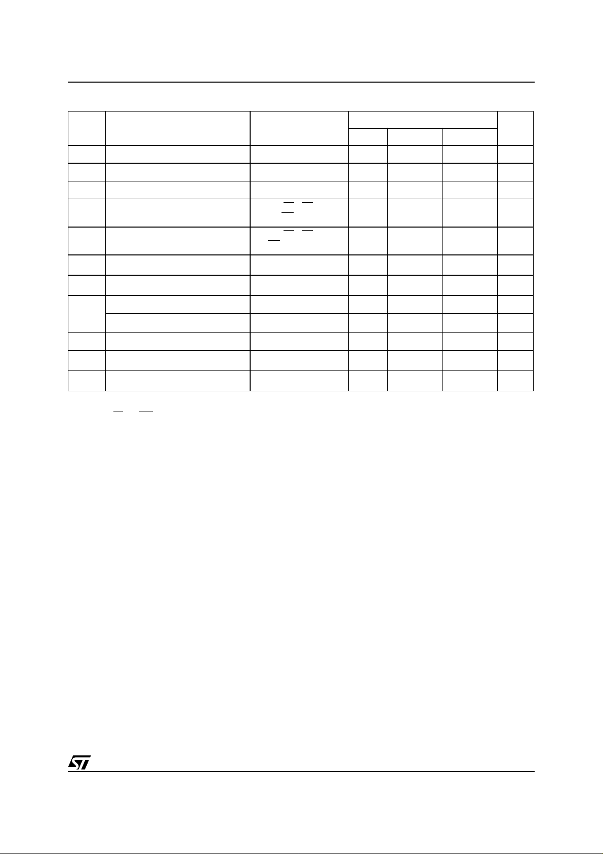
Table 11. DC Characteristics
M440T1MV
512mA
23mA
IN
CCI
≤ V
≤ V
IH
– 0.2
(1)
Min Typ Max
CC
CC
2.2 V
Sym Parameter
I
Input Leakage Current
LI
I
Output Leakage Current
LO
I
I
I
V
V
Supply Current 210 mA
CC1
Supply Current (TTL Standby)
CC2
CC3VCC
(2)
IL
(2)
IH
Power Supply Current
Input Low Voltage –0.3 0.6 V
Input High Voltage 2.2
Output Low Voltage
V
OL
Output Low Voltage (Open drain)
V
V
PFD
V
Note: 1. Vali d fo r Ambient Operating Temperature: TA = –15 to 75°C; VCC = 3.0 to 3. 6V (excep t where not e d).
Output High Voltage
OH
(2)
Power Fail Deselect 2.80 2.97 V
(2)
Battery Back-up Switchover 2.5 V
SO
2. All voltages are ref erenced to G round.
3. F or BL
and IRQ (Open drain); if pulled-up to supply other than VCC, this sup ply must be equal to , o r less than 3.0V when VCC = 0V
(during battery back-up mode).
Test Condition
(3)
0V ≤ V
0V ≤ V
E1
EC
E1
= V
EC
I
= 2.0mA
OL
IOL = 10mA
I
= –1.0mA
OH
OUT
- E4,
= V
- E4,
M440T1MV
±4 µA
±4 µA
+ 0.3
V
CC
0.4 V
0.4 V
Unit
V
19/26
Page 20
M440T1MV
Data Retention Mode
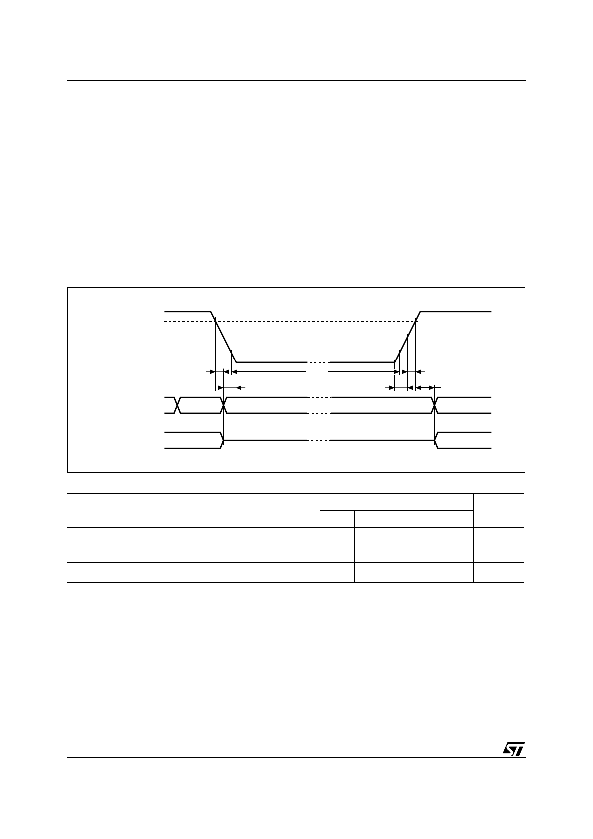
Should the supply voltage decay, the RAM will automatically deselect, write protecting itself when
falls between V
V
CC
dow. All outputs become high impedance an d all
inputs are treated as “Don't care.”
Note: A power failure during a WRITE cycle may
corrupt data at the current addressed location, but
does not jeopardize the rest of the RAM's content.
At voltage s belo w V
in a write protected state, provided the V
time is not less than t
spond to transient noise s pi kes on V
into the deselect window during the time the device is sampling V
Figure 15. Power Down/Up Mode AC Waveforms
V
CC
V
(max)
PFD
V
(min)
PFD
VSO
V
SS
INPUTS
(max), V
PFD
(min), the memory will be
PFD
. The M44 0T1MV may r e-
F
.Therefore, decoupling of the
CC
tF
(min) win-
PFD
that cr os s
CC
tFB
CC
fall
power supply lines is recomm ended. When V
CC
drops below VSO, the control circuit switches power to the internal battery, preserving data and powering the clock. The internal energy source will
maintain data in the M440T1MV for an accumulated period o f 5 years at 45°C. As system power rises above V
power supply is switched to e xternal V
protection continues until V
plus t
ER
after VCC exceeds V
t
ER
, the battery is disconnected, and the
SO
reaches V
CC
CC
PFD
. Write
(min)
(min). Normal RAM operation can resume
(max). Refer to Appli-
PFD
cation Note (AN1012) on the ST Web Site for more
information on battery life.
tDR
tRB
DON'T CARE
tR
tREC
RECOGNIZEDRECOGNIZED
OUTPUTS
VALID VALID
HIGH-Z
Table 12. Power Down/Up Trip Points DC Characteristics
Symbol
V
PFD
V
SO
t
DR
Note: 1. Vali d fo r Ambient Operating Temperature: TA = –15 to 75°C; VCC = 3.0 to 3. 6V (excep t where not e d).
2. All voltages referenced to V
3. At 45°C, V
Power-fail Deselect Voltage 2.8 2.9 2.97 V
Battery Back-up Switchover Voltage 2.5 V
(3)
Expected Data Retention Time 5 YEARS
= 0V.
CC
Parameter
.
SS
(1,2)
Min Typ Max
M440T1MV
AI04792
Unit
20/26
Page 21

Table 13. Power Down/Up AC Characteristics
Fall Time
CC
(1)
Min Max Unit
300 µs
10 µs
10 µs
1µs
Symbol
(2)
t
F
t
FB
t
R
t
RB
t
REC
Note: 1. Vali d fo r Ambient Operating Temperature: TA = –15 to 75°C; VCC = 3.0 to 3. 6V (excep t where not e d).
2. V
3. V
V
(max) to V
PFD
(3)
V
(min) to VSS VCC Fall Time
PFD
V
(min) to V
PFD
VSS to V
PFD
(min) V
Power-up Deselect Time 40 200 ms
(max) to V
PFD
(min).
es V
PFD
(min) to VSS fall time of less than tFB may cause corruption of RA M data.
PFD
(min) fall time of less than tF may result in deselection/write protection not occurring until 200µs after VCC pass-
PFD
Parameter
(min) V
PFD
(max) VCC Rise Time
PFD
Rise Time
CC
M440T1MV
21/26
Page 22
M440T1MV
PACKAG E MECHANICAL INFORMAT ION
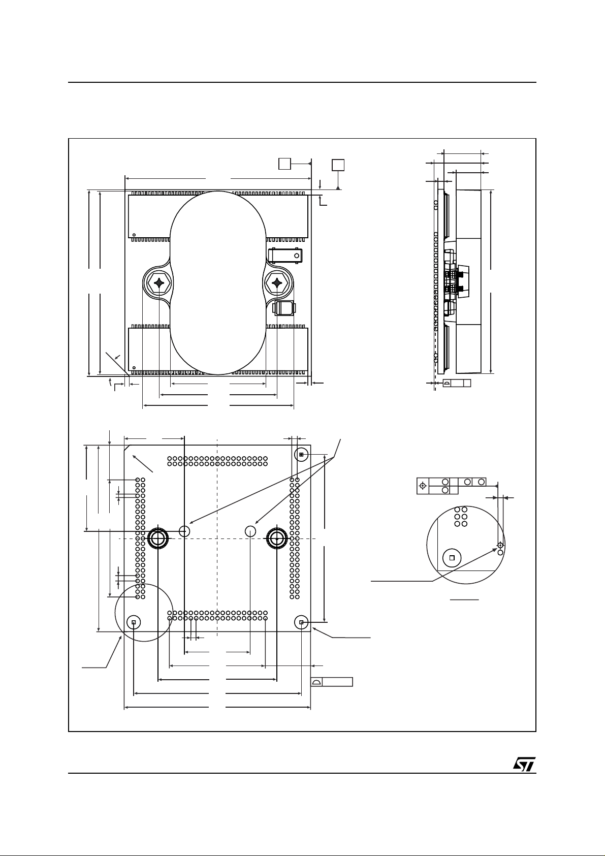
Figure 16. PBGA-ZA – 168-ball Plastic Ball Grid Array Package Outline
A
B
E
A
A1
A2
HE
A3
D
B
45˚
ddd
SIDE VIEW
FD
GE
E5
B3
B2
B1
TOP VIEW
GD
Non-plated
e
thru holes
B
C
1
BALL 1
D3
CORNER
b
D
D1
e
Detail A
Note: Drawing is not to scale.
22/26
e
E4
E1
E2
E3
E
BOTT OM VIEW
D2
FE
0.20 (4X)
Fiducial and
Soldermask
opening (3X)
SOLDER BALL (Typ)
eee
fff
C
S
C
DETAIL A
SS
A
B
PBGA-Z04
S
b
Page 23
Table 14. PBGA-ZA – 168-ball Plastic Ball Grid Array Package Mechanical Data
mm inches
Symb
Typ Min Max Typ Min Max
A 11.64 11.24 12.04 0.458 0.443 0.474
A1 6.60 6.30 6.90 0.260 0.248 0.272
A2 1.50 1.40 1.60 0.059 0.055 0.063
A3 9.25 9.00 9.50 0.364 0.354 0.374
B 44.40 44.30 44.50 1.748 1.744 1.752
B1 36.60 36.50 36.70 1.441 1.437 1.445
B2 28.25 28.15 28.35 1.112 1.108 1.116
B3 23.10 23.00 23.20 0.909 0.906 0.913
b 0.76 0.71 0.81 0.030 0.028 0.032
D 44.50 44.30 44.70 1.752 1.744 1.760
D1 27.94 1.100
D2 40.00 39.80 40.20 1.575 1.567 1.583
D3 20.56 20.46 20.66 0.809 0.806 0.813
e 1.27 0.050
M440T1MV
E 44.50 44.30 44.70 1.752 1.744 1.760
E1 22.86 0.900
E2 28.40 1.118
E3 40.00 39.80 40.20 1.575 1.567 1.583
E4 15.75 15.65 15.85 0.620 0.616 0.624
E5 14.38 14.28 14.48 0.566 0.562 0.570
FD 8.28 8.08 8.48 0.326 0.318 0.334
FE 10.82 10.72 10.92 0.426 0.422 0.430
GD 0.85 0.65 1.05 0.033 0.026 0.041
GE 1.00 0.039
HE 1.32 1.12 1.52 0.052 0.044 0.060
n 168 168
Tolerance Tolerance
ddd 0.15 0.006
eee 0.25 0.010
fff 0.10 0.004
23/26
Page 24

M440T1MV
PART NUMBERING
Table 15. Ordering Information Scheme
Example: M440T 1MV –15 ZA 9
Device Type
M440T
Supply Voltage and Write Protect Voltage
1MV = V
Speed
–15 = 150ns
= 3.0 to 3.6V; V
CC
= 2.8 to 2.97V
PFD
Package
ZA = 168-ball Ball Grid Array
Temperature Range
9 = –15 to 75 °C
Note: 1. Where “Z” is the symb ol for PBGA packages and “A” denotes 1.27mm ball pitch
(1)
For other options, or for more information on any aspect of this device, please contact the ST Sales Office
nearest you.
24/26
Page 25

REVISION HISTORY
Table 16. Document Revision History
Date Version Revision Details
September 2002 1.0 First issue
16-Jan-03 1.1 Modify mechanical data (Table 14)
31-Mar-03 1.2 Update test condition (Table 12)
11-Apr-03 2.0 Updated with template v2.2
05-Oct-04 3.0 Reformatted; update mechanical dimensions (Figure 16; Table 14)
M440T1MV
25/26
Page 26

M440T1MV
Information furnished is believed to be accurate and reliable. However, STMicroelectronics a ssumes no responsibility fo r the c onsequences
of use of such information nor for any infringement of patents or other rights of third parties which may result from its use. No license is granted
by implication or otherwise under any patent or patent rights of STMicroelectronics. Specifications mentioned in this publication are subject
to change without notice. This publication supersedes and replaces all information previously supplied. STMicroelectronics products are not
authori zed for use as criti cal component s in life support devices or sys tems without express written approval of STMicroele ct ronics.
The ST logo is a registered trademark of STMi croelectronics.
All other nam es are the property of their r espective owners
© 2004 STMi croelectroni cs - All rights reserved
Australi a - Belgium - Brazil - Canada - China - Czech Republic - Finl and - France - Germany - Hong Kong - India - Israel - Italy - Japan -
Malaysia - M al ta - Morocco - Singapore - Sp ai n - S weden - Swit zerland - United Kingdom - United States of America
STMicroelectronics group of companies
www.st.com
26/26
 Loading...