

Page 1

Owner’s Guide 0300179-01 Rev . B
™
PLC-5
A
NALOG INPUT
Catalog Numbers
1771sc-IFE32
32 C
HANNEL
M
ODULE
Page 2

Page 3

Important Notes
1. Please read all the information in this owner’s guide before installing
the product.
2. The information in this owner's guide applies to hardware and
firmware version 1.0 or later.
3. This guide assumes that the reader has a full working knowledge of
the relevant processor.
Notice
The products and services described in this owner's guide are useful in a
wide variety of applications. Therefore, the user and others responsible
for applying the products and services described herein are responsible
for determining their acceptability for each application. While efforts
have been made to provide accurate information within this owner's
guide, Spectrum Controls assumes no responsibility for the accuracy,
completeness, or usefulness of the information herein.
Under no circumstances will Spectrum Controls be responsible or liable
for any damages or losses, including indirect or consequential damages
or losses, arising out of either the use of any information within this
owner's guide or the use of any product or service referenced herein.
No patent liability is assumed by Spectrum Controls with respect to the
use of any of the information, products, circuits, programming, or
services referenced herein.
The information in this owner's guide is subject to change without notice.
Limited Warranty
Spectrum Controls warrants that its products are free from defects in
material and workmanship under normal use and service, as described in
Spectrum Controls literature covering this product, for a period of 1 year.
The obligations of Spectrum Controls under this warranty are limited to
replacing or repairing, at its option, at its factory or facility, any product
which shall, in the applicable period after shipment, be returned to the
Spectrum Controls facility, transportation charges prepaid, and which
after examination is determined, to the satisfaction of Spectrum Controls,
to be thus defective.
This warranty shall not apply to any such equipment which shall have
been repaired or altered except by Spectrum Controls or which shall
have been subject to misuse, neglect, or accident. In no case shall the
liability of Spectrum Controls exceed the purchase price. The
aforementioned provisions do not extend the original warranty period of
any product which has either been repaired or replaced by Spectrum
Controls.
Page 4

Page 5

Important User Information
Because of the variety of uses for the products described in this publication, those
responsible for the application and use of this control equipment must satisfy
themselves that all necessary steps have been taken to assure that each application
and use meets all performance and safety requirements, including any applicable
laws, regulations, codes and standards.
The illustrations, charts, sample programs and layout examples shown in this guide
are intended solely for example. Since there are many variables and requirements
associated with any particular installation, Spectrum Controls does not assume
responsibility or liability (to include intellectual property liability) for actual use based
upon the examples shown in this publication.
Allen-Bradley publication SGI–1.1, “Safety Guidelines For The Application, Installa-
tion and Maintenance of Solid State Control” (available from your local Allen-Bradley
office) describes some important differences between solid-state equipment and
electromechanical devices which should be taken into consideration when applying
products such as those described in this publication.
Reproduction of the contents of this copyrighted publication, in whole or in part,
without written permission of Spectrum Controls, is prohibited.
Preface: Important User Information v
Preface
Throughout this manual we make notes to alert you to possible injury to people or
damage to equipment under specific circumstances.
ATTENTION: Identifies information about practices or circumstances that can lead to
!
Attention helps you:
· identify a hazard
· avoid the hazard
· recognize the consequences
Important: Identifies information that is especially important for successful application and understanding of the product.
Important: We recommend you frequently backup your application programs on
appropriate storage medium to avoid possible data loss.
personal injury or death, property damage, or economic loss.
Page 6

vi PLC-5
TM
32-Channel Analog Input Module
Page 7

Using This Manual v
Using This Manual
Purpose of Manual:Purpose of Manual:
Purpose of Manual:
Purpose of Manual:Purpose of Manual:
This manual shows you how to use your Analog Input module with an Allen-Bradley
programmable controller. It helps you install, program, calibrate, and troubleshoot
your module.
Audience:Audience:
Audience:
Audience:Audience:
Y ou must be able to program and operate an Allen-Bradley programmable controller to
make efficient use of your input module. In particular , you must know how to
program block transfers. We assume that you know how to do this in this manual. If
you do not, refer to the appropriate programming and operations manual before you
attempt to program this module.
VV
ocabocab
ularular
ular
ularular
y:y:
y:
y:y:
V
ocab
VV
ocabocab
In this manual, we refer to:
· The analog input module as the “input module” or the “module”
· The programmable controller as the “controller”
Manual Organization:Manual Organization:
Manual Organization:
Manual Organization:Manual Organization:
This manual is divided into seven chapters. The following chart shows each chapter
with its corresponding title and a brief overview of the topics covered in that chapter.
Chapter Title Topics Covered
1 Overview of Analog Input modules Description of module including general and
2 Installing the Module Module power requirements, keying, chassis
3 Module Programming Sample Programs
4 Configuring Your Module Hardware and Software Configuration Input range
5 Module Status and Input Data Reading Data from the Module Read block format
6 Calibrating Your Module Information on Calibrating your Module
7 Troubleshooting Your Module Troubleshooting guide for problem diagnosis
Appendix Title Topics Covered
A Specifications
Product CompatibilityProduct Compatibility
Product Compatibility
Product CompatibilityProduct Compatibility
hardware features
location. Wiring of the terminal block
Selection
The 1771-IFE 32 module can be used with any 1771 I/O chassis. Communication
between the discrete analog module and the processor is bi-directional; the processor
block-transfers output data through the output image table to the module and blocktransfers input data from the module through the input image table. The module also
requires an area in the data table to store the read block transfer data and write block
transfer data. I/O image table use is an important factor in module placement and
addressing selection.
You can place your input module in any I/O module slot of the I/O chassis. You can
put two input modules in the same module group. You can put an input and an
output module in the same module group.
Do not put the module in the same module group as a discrete high-density module.
Avoid placing analog input modules close to ac modules or high voltage dc modules.
Page 8

vi PLC-5
TM
32-Channel Analog Input Module
Related PublicationsRelated Publications
Related Publications
Related PublicationsRelated Publications
For a list of publications with information on Allen-Bradley programmable controller
products, consult our publication index (SD499).
Page 9

Contents
Preface................................................................................................................................................................v
Important User Information............................................................................................................................v
Using This Manual ...........................................................................................................................................v
Chapter 1 Overview of the Analog Input Module ......................................................................................1
Module Description ...............................................................................................................................................................1
Features ................................................................................................................................................................................. 1
Program Selectable Input Ranges .......................................................................................................................................... 2
How Analog Modules Communicate with Programmable Controllers ...................................................................................2
Accuracy ...............................................................................................................................................................................3
Chapter Summary ................................................................................................................................................................... 3
Chapter 2 Installing the Input Module ........................................................................................................5
Power Requirements: ............................................................................................................................................................. 6
Locating the Module in the I/O Chassis ................................................................................................................................7
Key the Backplane Connector ...............................................................................................................................................7
Wiring Your Analog Module .................................................................................................................................................. 7
T o minimize ground-loop currents on input circuits: .............................................................................................................8
Cable Lengths ........................................................................................................................................................................8
Grounding ............................................................................................................................................................................11
Indicator Lights:................................................................................................................................................................... 11
Chapter Summary ................................................................................................................................................................. 12
Chapter 3 Module Programming ................................................................................................................13
Block Transfer Programming................................................................................................................................................ 13
Module Scan Time ............................................................................................................................................................... 15
Chapter Summary ................................................................................................................................................................. 15
Chapter 4 Configuring Your Module ..........................................................................................................17
Configuring your input module:........................................................................................................................................... 17
Block Transfer W rite (BTW) Maps ...................................................................................................................................... 17
Configuration W ord ............................................................................................................................................................. 18
Input Range Selection.......................................................................................................................................................... 18
Data Format: ......................................................................................................................................................................... 20
Digital Filtering:.................................................................................................................................................................... 20
Automatic System Calibration .............................................................................................................................................21
(Autocal) .............................................................................................................................................................................. 21
Debug Flags......................................................................................................................................................................... 21
Real Time Sampling: ............................................................................................................................................................. 23
Scale W ord Configuration Bits ............................................................................................................................................ 25
Default Configuration: .........................................................................................................................................................25
Chapter Summary ................................................................................................................................................................. 26
Chapter 5 Module Status and Input Data .................................................................................................27
Reading Data from Y our Module ......................................................................................................................................... 27
Block Transfer Read (BTR) Maps ........................................................................................................................................ 27
Module Data BTR ................................................................................................................................................................ 27
Module Data/Configuration Echo BTR................................................................................................................................ 28
Page 10

Chapter 6 Troubleshooting Your Input Module .......................................................................................29
Diagnostics Reported by the Module.................................................................................................................................. 29
Diagnostic Bits Reported by the Analog input .................................................................................................................... 29
Checking Module Operation................................................................................................................................................ 31
Testing for Input.................................................................................................................................................................. 33
Channel Functionality.......................................................................................................................................................... 33
Chapter Summary ................................................................................................................................................................. 33
Appendix A ......................................................................................................................................................35
Electrical Specs .................................................................................................................................................................... 35
System Specifications .......................................................................................................................................................... 36
3.3 Environmental Specifications ......................................................................................................................................... 36
T erminal Block Pinouts ........................................................................................................................................................ 37
Declaration of Conformity .............................................................................................................................39
Page 11

Overview of the Analog Input Module
Chapter Objectives
This chapter, we describe:
· features of the module
· how the module communicates with programmable controllers
Module Description
The analog input module is an intelligent block transfer module that interfaces analog
input signals with any Allen-Bradley programmable controllers that have block
transfer capability . Block transfer programming moves input data words from the
module’s memory to a designated area in the processor data table in a single scan. It
also moves configuration words from the processor data table to module memory.
The input module is a single-slot module and requires no external power supply . (If
using passive transducers for input, the user must supply loop power.) After scanning the analog inputs, the input data is converted to a specified data type in a digital
format to be transferred to the processor’s data table on request. The block transfer
mode is disabled until this input scan is complete. Consequently , the minimum
interval between block transfer reads is the same as the total input update time for
each analog input module.
Chapter 1: Overview of the Analog Input Module 1
Chapter 1
Features
The Analog input module senses up to 32 single-ended or 16 differential analog
inputs and converts them to a proportional four-digit BCD, 16 bit binary and 12 bit
binary formats. Y ou can select from five voltage or three current input ranges.
Channels may be configured to acquire data as singled-ended inputs or as differential
pairs. During differential acquisition, odd channels (1, 3, 5, etc.) are the positive input
and the even channels (2, 4, 6, etc.) the negative inputs. A channel pair consists of
two consecutive channels (1&2, 3&4, 5&6, etc.). Within a channel pair both channels
must be specified as single acquisition or both as differential acquisition. Within a
group of 8 consecutive channels, all 8 channels must be from either 8 voltage or 8
current sources. If part of a voltage group, a channel may be any of the allowed
voltage ranges and if in a current group a channel may be any of the allowed current
ranges as long as all 8 are either voltage ranges or all 8 are current ranges.
This module’s program selectable features include:
· 32 single-ended or 16 differential inputs
· User program selectable input ranges on a per channel basis (see table)
· Selectable real-time sampling
· Selectable scaling to engineering units
· Selectable digital filtering
· Selectable data format
Page 12
2 PLC-5
TM
32-Channel Analog Input Module
Program Selectable Input Ranges
Valid acquisition types/ranges are listed below:
Single Ended Ranges: Limits: Differential Ranges: Limits:
* = Default
** = Disabled. If this is the selected value, acquisition of this channel is disabled.
This can be used to
improve throughput in modules where some channels are not used.
NA = Not allowed.
How Analog Modules
Communicate with
Programmable Controllers
0* -10 to +10 V 8 -10 to +10 V
1 0 to +10 V 9 0 to +10 V
2 0 to +5 V 1 0 0 to +5 V
3 +1 to +5 V 11 +1 to +5 V
4 -5 to +5 V 12 -5 to +5 V
5 0 to +20 ma 1 3 NA
6 +4 to +20 ma 1 4 NA
7 -20 to +20 ma 1 5 **Disabled
The processor transfers data to the module (block transfer write) and from the module
(block transfer read) using BTW and BTR instructions in your ladder diagram
program. These instructions let the processor obtain input values and status from the
module, and let you establish the module’s mode of operation.
1. The processor transfers your configuration data to the module via a block transfer
write instruction.
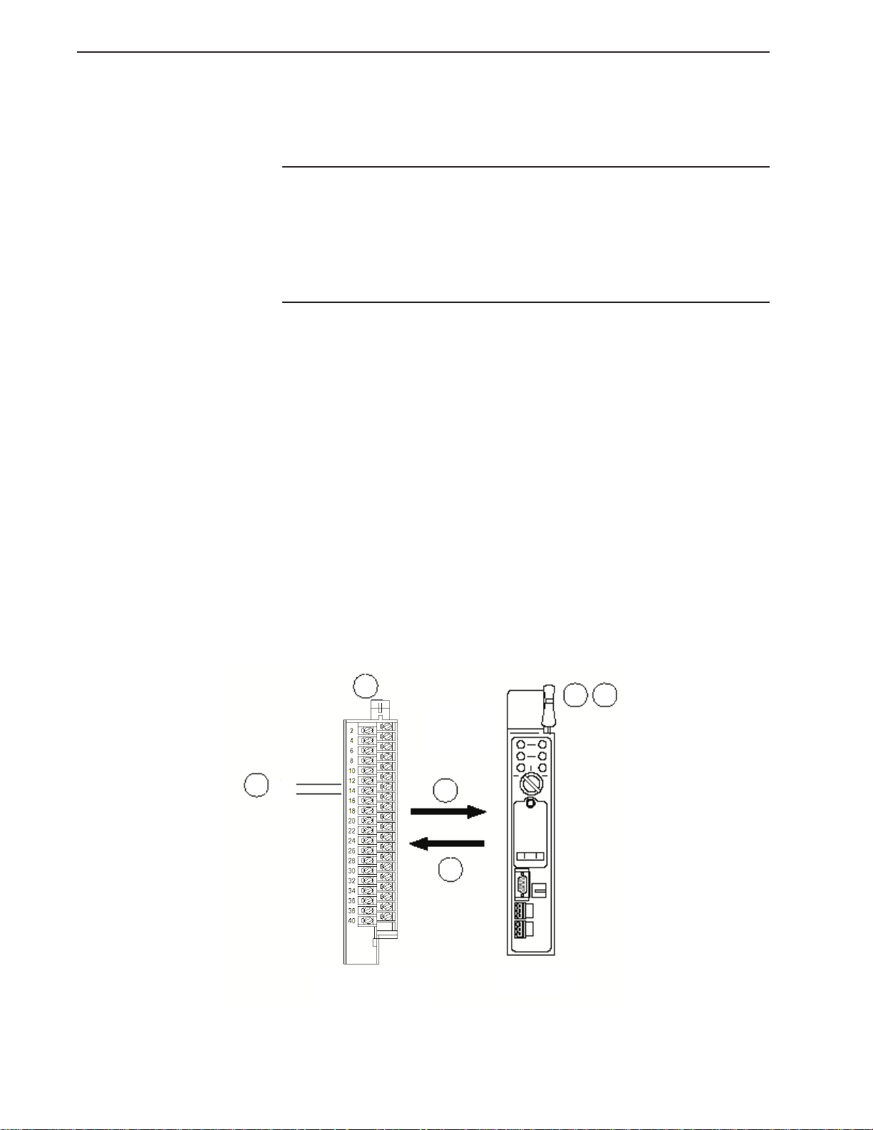
2. External devices generate analog signals that are transmitted to the module
3
I/O Chassis
Backplane
+
2
_
4
1
5 6
Input Module
1771sc-IFE32
PC Processor
Page 13

Accuracy
Chapter Summary
Chapter 1: Overview of the Analog Input Module 3
3. The module converts analog signals into binary or BCD format, and stores these
values until the processor requests their transfer.
4. When instructed by your ladder program, the processor performs a read block
transfer of the values and stores them in a data table.
5. The processor and module determine that the transfer was made without error, and
that input values are within specified range.
6. Y our ladder program can use and/or move the data (if valid) before it is written over
by the transfer of new data in a subsequent transfer.
7. Y our ladder program should allow write block transfers to the module only when
enabled by operator intervention or at power-up.
The accuracy of your input module is described in Appendix A.
In this chapter you read about the functional aspects of the input module and how
the module communicates with the programmable controller .
Page 14

4 PLC-5
TM
32-Channel Analog Input Module
Page 15

Installing the Input Module
Chapter Objectives
Chapter 2: Installing the Input Module 5
Chapter 2
In this chapter, we tell you about:
· calculating the chassis power requirement
· choosing the module’s location in the I/O chassis
· configuring your module configuration plugs
· keying a chassis slot for your module
· installing the input module
· wiring the input module’s field wiring arm
Compliance to European Union Directives
If this product has the CE mark it is approved for installation within the European
Union and EEA regions. It has been designed and tested to meet the following
directives.
EMC Directive
This product is tested to meet Council Directive 89/336/EEC Electromagnetic Compatibility (EMC) and the following standards, in whole or in part, documented in a
technical construction file:
· EN 50081-2EMC – Generic Emission Standard, Part 2 –Industrial Environment
· EN 50082-2EMC – Generic Immunity Standard, Part 2 – Industrial Environment
Before Y ou Install
Y our Input Module
This product is intended for use in an industrial environment.
Before installing your input module in the I/O chassis:
You need to: As described under:
Calculate the power requirements of all modules in the chassis. Power requirements, page….
Determine were to place the I/O module in the chassis Module locating in the I/O chassis, page…
Key the backplane connector to the I/O chassis Module Keying, page….
Make connections to the wiring arm Wiring your input module, page… and
grounding, page…
Important:
The 1771-IFE32 module is shipped from the factory set for voltage mode applications. Refer to “Setting the Configuration on the Module”on page 2–3 for other
combinations of current and voltage inputs.
Electrostatic Damage:
Electrostatic discharge can damage semiconductor devices inside this module if you
touch backplane connector pins. Guard against electrostatic damage by observing
the following precautions:
Page 16

6 PLC-5
TM
32-Channel Analog Input Module
!
• Wear an approved wrist strap grounding device, or touch a grounded object to rid yourself of
• Handle the module from the front, away from the backplane connector. Do not touch backplane
• Keep the module in its static-shield bag when not in use.
!
• Peripheral equipment must be suitable for the location in which it is used.
ATTENTION: Electrostatic discharge can degrade performance or cause permanent damage.
Handle the module as stated below.
electrostatic charge before handling the module.
connector pins.
WARNING: Power, input and output (I/O) wiring must be in accordance with Class I, Division 2
wiring methods (Article 501-4(b) of the National Electrical Code, NFPA 70) and in accordance
with the authority having jurisdiction.
Power Requirements:
WARNING – EXPLOSION HAZARD – SUBSTITUTION OF COMPONENTS MA Y IMP AIR
SUIT ABLIITY FOR CLASS I, DIVISION 2
!
WARNING – EXPLOSION HAZARD – WHEN IN HAZARDOUS LOCA TIONS, TURN OFF POWER
BEFORE REPLACING OR WIRING MODULES.
!
WARNING – EXPLOSION HAZARD – DO NOT DISCONNECT EQUIPMENT UNLESS POWER HAS
!
BEEN SWITCHED OFF OR THE AREA IS KNOWN TO BE NON-HAZARDOUS.
THIS EQUIPMENT IS SUIT ABLE FOR USE IN CLASS I, DIVISION 2, GROUPS A, B, C, AND D OR
!
NON-HARZARDOUS LOCATIONS ONLY .
Y our module receives its power through the 1771 I/O power supply. The module
requires a maximum of 400mA from the backplane.
Add this current to the requirements of all other modules in the I/O chassis to prevent
overloading the chassis backplane and/or backplane power supply.
Page 17

Locating the Module in
the I/O Chassis
Key the Backplane Connector
!
Chapter 2: Installing the Input Module 7
Place your module in any I/O module slot of the I/O chassis except for the extreme left
slot. This slot is reserved for PC processors or adapter modules.
Group your modules to minimize adverse affects from radiated electrical noise and
heat. W e recommend the following.
· Group analog input and low voltage dc modules away from ac modules or high
voltage dc modules to minimize electrical noise interference.
· Do not place this module in the same I/O group with a discrete high-density I/O
module when using 2-slot addressing. This module uses a byte in both the input
and output image tables for block transfer.
Place your module in any slot in the chassis except the leftmost slot, which is
reserved for processors or adapters.
ATTENTION: Observe the following precautions when inserting or removing keys:
· insert or remove keys with your fingers
· make sure that key placement is correct incorrect keying or the use of a tool can result in
damage to the backplane connector and possible system faults.
The 1771sc-IFE32 module is slitted at two places on the rear edge of the circuit board.
These slots mate with plastic keying bands which mount on the backplane connector.
Position the keying bands in the backplane connector to correspond to the key slots.
Keying Bands
ATTENTION: Insert or remove
keying bands with your fingers.
Upper Connector
Wiring Y our Analog Module
Connect your I/O devices to the cat. no. 1771-WG wiring arm shipped with the
module. The wiring arm is attached to the pivot bar at the bottom of the I/O chassis. It
pivots upward and connects with the module so you can install or remove the module
without disconnecting the wires. You may also use a prewired swing arm, AllenBradley part number 1492-cable[1]WN.
Page 18

8 PLC-5
TM
32-Channel Analog Input Module
!
· Failure to remove power from the backplane or wiring arm could cause module damage,
· Failure to remove power from the backplane could cause injury or equipment damage due to
ATTENTION:
Remove power from the 1771 I/O chassis backplane and field-wiring arm before removing or
installing an I/O module.
degradation of performance, or injury.
possible unexpected operation.
Place the module in the card guides on the top
and bottom of the slot that guide the 1771sc-IFE32 module in position
To minimize ground-loop
currents on input circuits:
Cable Lengths
· use differential mode
· use 2-wire transmitters with a common power supply
· separate 2-wire and 4-wire transmitters between different modules
· tie 4-wire transmitter and/or separate power supply grounds together
Important:
W e do not recommend mixing 2-wire and 4-wire transmitter inputs on the same
module. Power supply placement can make it impossible to eliminate ground loops.
Recommended maximum cable length for voltage-mode input devices is 50 feet. This
recommendation is based on considerations of signal degradation and electrical noise
Page 19

Chapter 2: Installing the Input Module 9
immunity in typical industrial environments. Cable length for current-mode input
devices need not be as restrictive because analog signals from these devices are less
sensitive to electrical noise interference.
Input connections for the 1771sc-IFE32 module with single-ended and differntial
inputs are shown in the following figures.
Connection Diagram for 32 Single-ended
Inputs and Two-wire Transmitters
2-Wire
Transmitter
2-Wire
Transmitter
Commons are tied in groups of four inside the module. Jumper all
unused channels to appropriate group common to reduce noise.
Tie power supply grounds together to minimize ground loops.
Attention: This signle includes any common mode voltage
present between either input terminal and module common.
If an input exceeds this range channel-to-channel cross talk
can cause invalid input readings and invalid under or over range
readings.
The sensor cable must be shielded. The shield must extend
the length of the cable to the point of termination.
Power
Supply
Power
Supply
+
-
+
-
Source Ground
Connection Diagram for 32 Single-ended
Inputs and Four-wire Transmitters
Channel 2
Channel 4
Channel 5
Channel 7
Common Group 1
Channel 10
Channel 12
Channel 13
Channel 15
Common Group 2
Channel 18
Channel 20
Channel 21
Channel 23
Common Group 3
Channel 26
Channel 28
Channel 29
Channel 31
Common Group 4
Channel 1
Channel 3
Common Group 1
Channel 6
Channel 8
Channel 9
Channel 11
Common Group 2
Channel 14
Channel 16
Channel 17
Channel 19
Common Group 3
Channel 22
Channel 24
Channel 25
Channel 27
Common Group 4
Channel 30
Channel 32
Power
4-Wire
Supply
Transmitter
4-Wire
Power
Transmitter
Supply
Commons are tied in groups of four inside the module. Jumper all
unused channels to appropriate group common to reduce noise.
Tie power supply grounds together to minimize ground loops.
Attention: This signle includes any common mode voltage
present between either input terminal and module common.
If an input exceeds this range channel-to-channel cross talk
can cause invalid input readings and invalid under or over range
readings.
The sensor cable must be shielded. The shield must extend
the length of the cable to the point of termination.
+
-
+
-
Source Ground
Channel 2
Channel 4
Channel 5
Channel 7
Common Group 1
Channel 10
Channel 12
Channel 13
Channel 15
Common Group 2
Channel 18
Channel 20
Channel 21
Channel 23
Common Group 3
Channel 26
Channel 28
Channel 29
Channel 31
Common Group 4
Channel 1
Channel 3
Common Group 1
Channel 6
Channel 8
Channel 9
Channel 11
Common Group 2
Channel 14
Channel 16
Channel 17
Channel 19
Common Group 3
Channel 22
Channel 24
Channel 25
Channel 27
Common Group 4
Channel 30
Channel 32
Page 20

10 PLC-5
A
A
TM
32-Channel Analog Input Module
Connection Diagram for 16 Differential
Inputs and Two-wire Transmitters
2-Wire
Transmitter
+
2-Wire
Transmitter
+
ll unsed inputs should have their + and - inputs tied together
and to Commons to reduce noise. Tie power supply grounds
together to minimize ground loops.
ttention: This signal must be between +14.5V and common voltage
otherwise channel-to-channel cross talk can cause invalid input
readings and invalid under or over range readings.
The sensor cable must be shielded. The shield must extend
the length of the cable to the point of termination.
+
+
Power
Supply
Power
Supply
-
-
-
-
Source Ground
Connection Diagram for 16 Differential
Inputs and Four-wire Transmitters
Input 1-
Input 2-
Input 3+
Input 4+
Common Group 1
Input 5-
Input 6-
Input 7+
Input 8+
Common Group 2
Input 9-
Input 10-
Input 11+
Input 12+
Common Group 3
Input 13-
Input 14-
Input 15+
Input 16+
Common Group 4
Input 1+
Input 2+
Input 3-
Input 4-
Common Group 1
Input 5+
Input 6+
Input 7-
Input 8-
Common Group 2
Input 9+
Input 10+
Input 11-
Input 12-
Common Group 3
Input 13+
Input 14+
Input 15-
Input 16-
Common Group 4
Input 1-
Input 2-
Power
4-Wire
Supply
Transmitter
4-Wire
Power
Transmitter
Supply
All unsed inputs should have their + and - inputs tied together
and to Commons to reduce noise. Tie power supply grounds
together to minimize ground loops.
Attention: This signal must be between +14.5V and common voltage
otherwise channel-to-channel cross talk can cause invalid input
readings and invalid under or over range readings.
The sensor cable must be shielded. The shield must extend
the length of the cable to the point of termination.
+
-
+
-
Source Ground
Input 3+
Input 4+
Common Group 1
Input 5-
Input 6-
Input 7+
Input 8+
Common Group 2
Input 9-
Input 10-
Input 11+
Input 12+
Common Group 3
Input 13-
Input 14-
Input 15+
Input 16+
Common Group 4
Input 1+
Input 2+
Input 3-
Input 4-
Common Group 1
Input 5+
Input 6+
Input 7-
Input 8-
Common Group 2
Input 9+
Input 10+
Input 11-
Input 12-
Common Group 3
Input 13+
Input 14+
Input 15-
Input 16-
Common Group 4
Page 21

Grounding
Chapter 2: Installing the Input Module 11
When using shielded cable wire, ground the foil shield and drain wire only at one end
of the cable. We recommend that you wrap the foil shield and drain wire together, and
connect them to a chassis mounting bolt, grounding stud or chassis single-point
grounding point (Figure 2.5). Use heat shrink tubing to seal the exit point of the wires.
At the opposite end of the cable, tape exposed shield and drain wire with electrical
tape to insulate it from electrical contact.
Indicator Lights:
Chapter Summary
The front panel of the analog input module contains a green RUN indicator and a red
F AUL T indicator . At power-up an initial module self-check occurs. If there is no fault,
the red indicator turns off.
The green indicator comes on when the module is powered. It will flash until the
module is programmed. If a fault is found initially or occurs later, the red fault indicator lights. Possible module fault causes and corrective action is discussed in Chapter
6, Troubleshooting.
In this chapter you learned how to install your input module in an existing programmable controller system and how to wire the field swing arm.
Page 22

12 PLC-5
TM
32-Channel Analog Input Module
Page 23

Module Programming
BlocBloc
k k
TT
ransfransf
er Prer Pr
Bloc
BlocBloc
k
k k
T
ransf
TT
ransfransf
ogrammingogramming
er Pr
ogramming
er Prer Pr
ogrammingogramming
Chapter 3: Module Programming 13
Chapter 3
Chapter Objectives:Chapter Objectives:
Chapter Objectives:
Chapter Objectives:Chapter Objectives:
In this chapter we describe:
· block transfer programming
· sample programs for PLC-5 processors
· module scan time issues
Y our module communicates with your processor through bi-directional block transfers. This is the sequential operation of both read and write block transfer instructions.
The block transfer write (BTW) instruction is initiated when the analog module is first
powered up, and subsequently only when the programmer wants to write a new
configuration to the module. At all other times the module is basically in a repetitive
block transfer read (BTR) mode.
The application programs for the three processor families were written to accomplish
this handshaking in the described manner . They are minimum programs; all the rungs
and conditioning must be included in your application program. If you wish to disable
BTRs for any reason, or add interlocks to the BTW rung to prevent writes from
happening at certain times, you are allowed to do it. You may not eliminate any
storage bits or interlocks that are included in our examples. If interlocks are removed,
the program may not work properly .
The analog input module’s green LED will flash unit the module is programmed.
The module will work with a default configuration of zeroes entered in all five words
of a five word BTW configuration block. Upon writing zeros to the configuration
word the LED will stop blinking. See the configuration default section to understand
what this configuration will look like. Also, refer to Appendix C for example configuration blocks and instruction addresses to get started.
Page 24

14 PLC-5
TM
32-Channel Analog Input Module
PLC-5 Programming:
The PLC-5 program is very straight forward with the following exceptions:
1. You must use enable bits instead of done bits as the conditions on each rung.
2. A separate control file must be selected for each of the block transfer instructions.
Page 25

Chapter 3: Module Programming 15
Module Scan Module Scan
Module Scan
Module Scan Module Scan
TimeTime
Time
TimeTime
Update time is defined as the amount of time it takes for the input module to read the
input channels and place new data into the data buffer . Scan time for your module is
shown in Appendix A.
Following a block transfer write “1” the module inhibits communication until after it
has configured the data “2,” performed calibration check “3” (if requested), scanned
the inputs “4,” and filled the data buffer “5.” Write block transfers, therefore, should
only be performed when the module is being configured or calibrated.
Any time after the second scan begins “6,” a BTR request “7” can be acknowledged.
This interrupts the scan and the BTR empties the buffer . (If R TS is enabled, a BTR will
only occur after the specified time period. Refer to chapter 4.)
Following the BTR, the input module inhibits block transfer communications with the
programmable controller until it has scanned its inputs “8” and new data is ready ”9.”
The input module repeats the scan sequence “10,” updating the input values until
another block transfer request is received. Therefore, BTRs will only be completed as
frequently as the total update time of the input module.
Chapter SummaryChapter Summary
Chapter Summary
Chapter SummaryChapter Summary
In this chapter, you learned to program your programmable controller . You were given
a sample program for your PLC-5 processor.
Page 26

16 PLC-5
TM
32-Channel Analog Input Module
Page 27

Configuring Y our Module
Configuring yourConfiguring your
Configuring your
Configuring yourConfiguring your
input module:input module:
input module:
input module:input module:
Chapter 4
Chapter Objectives:Chapter Objectives:
Chapter Objectives:
Chapter Objectives:Chapter Objectives:
In this chapter, we describe;
· configuring your module’s features
· conditioning your inputs
· entering your data.
Because of the many analog devices available and the wide variety of possible
configurations, you must configure your module to conform to the analog device and
specific application that you have chosen. Data is conditioned through a group of
data table words that are transferred to the module using a block transfer write
instruction.
The software configurable features available with the Analog Input Module (cat. no.
1771sc-IFE32 are:
· input range selection
· input type
· data format
· digital filtering
· real time sampling
· scaling to engineering units
BlocBloc
k k
TT
k
k k
ransfransf
T
ransf
TT
ransfransf
Bloc
BlocBloc
(BTW) Maps(BTW) Maps
(BTW) Maps
(BTW) Maps(BTW) Maps
er er
er
er er
WriteWrite
Write
WriteWrite
T wo distinctly different block transfer writes (BTW) can be performed to configure
the module. The first, BTW1, configures the module.
During normal operation the processor transfers 0 to 22 words to the module when
you program a block transfer write instruction to the module’s address. This BTW file
contains configuration words for each channel.
When user-define scaling is used a second BTW word is required and it’s length is
64 words.
BTW: N Words: Purpose: Required?
BTW1 23 Module Configuration Required
BTW2 64 User Scaling Optional
Page 28

18 PLC-5
TM
32-Channel Analog Input Module
Configuration Configuration
Configuration
Configuration Configuration
WW
W
WW
oror
or
oror
dd
d
dd
The channel configuration word is described below:
Input T ype/Range must be configured using Binary or Hexidecimal values.
Word/Bit 15 14 13 12 11 10 09 08 07 06 05 04 03 02 01 00 Group
0 Channel 4 Channel 3 Channel 2 Channel 1 *Type/Range
1 Channel 8 Channel 7 Channel 6 Channel 5 *Type/Range
2 Channel 12 Channel 11 Channel 10 Channel 9 *Type/Range
3 Channel 16 Channel 15 Channel 14 Channel 13 *Type/Range
4 Channel 20 Channel 19 Channel 18 Channel 17 *Type/Range
5 Channel 24 Channel 23 Channel 22 Channel 21 *Type/Range
6 Channel 28 Channel 27 Channel 26 Channel 25 *Type/Range
7 Channel 32 Channel 31 Channel 30 Channel 29 *Type/Range
8 Channel 4 Channel 3 Channel 2 Channel 1 Data Format
9 Channel 8 Channel 7 Channel 6 Channel 5 Data Format
10 Channel 12 Channel 11 Channel 10 Channel 9 Data Format
11 Channel 16 Channel 15 Channel 14 Channel 13 Data Format
12 Channel 20 Channel 19 Channel 18 Channel 17 Data Format
13 Channel 24 Channel 23 Channel 22 Channel 21 Data Format
14 Channel 28 Channel 27 Channel 26 Channel 25 Data Format
15 Channel 32 Channel 31 Channel 30 Channel 29 Data Format
16 Chan 8 Chan 7 Chan 6 Chan 5 Chan 4 Chan 3 Chan 2 Chan 1 Filter Freq
17 Chan 16 Chan 15 Chan 14 Chan 13 Chan 12 Chan 11 Chan 10 Chan 9 Filter Freq
18 Chan 24 Chan 23 Chan 22 Chan 21 Chan 20 Chan 19 Chan 18 Chan 17 Filter Freq
19 Chan 32 Chan 31 Chan 30 Chan 29 Chan 28 Chan 27 Chan 26 Chan 25 Filter Freq
20 Automatic Calibration Rate Autocal
21 Debug Flags Debug Flags
22 Real Time Sampling RTS
Input Range SelectionInput Range Selection
Input Range Selection
Input Range SelectionInput Range Selection
Channels may be configured to acquire data as singled-ended inputs or as differential
pairs. During differential acquisition, odd channels (1, 3, 5, etc.) are the positive input
and the even channels (2, 4, 6, etc.) the negative inputs. A channel pair consists of
two consecutive channels (1&2, 3&4, 5&6, etc.). Within a channel pair both channels
must be specified as single acquisition or both as differential acquisition.
Word/Bit 15 14 13 12 11 10 09 08 07 06 05 04 03 02 01 00 Group
0 Channel 4 Channel 3 Channel 2 Channel 1 *Type/Range
1 Channel 8 Channel 7 Channel 6 Channel 5 *Type/Range
2 Channel 12 Channel 11 Channel 10 Channel 9 *Type/Range
3 Channel 16 Channel 15 Channel 14 Channel 13 *Type/Range
4 Channel 20 Channel 19 Channel 18 Channel 17 *Type/Range
5 Channel 24 Channel 23 Channel 22 Channel 21 *Type/Range
6 Channel 28 Channel 27 Channel 26 Channel 25 *Type/Range
7 Channel 32 Channel 31 Channel 30 Channel 29 *Type/Range
Several input ranges for voltage and current are supported. Ranges that include both
negative and positive values are referred to as bipolar ranges throughout this
document. Ranges that include only positive values are referred to as unipolar.
Within a group of 8 consecutive channels, all 8 channels must be from either 8
voltage or 8 current sources. If part of a voltage group, a channel may be any of the
allowed voltage ranges and if in a current group a channel may be any of the allowed
current ranges as long as all 8 are either voltage ranges or all 8 are current
Page 29

Chapter 4: Configuring Your Module 19
ranges.
Valid acquisition types/ranges are listed below:
Single Ended Ranges: Limits: Differential Ranges: Limits:
0* -10 to +10 V 8 -10 to +10 V
1 0 to +10 V 9 0 to +10 V
2 0 to +5 V 10 0 to +5 V
3 +1 to +5 V 11 +1 to +5 V
4 -5 to +5 V 12 -5 to +5 V
5 0 to +20 ma 13 NA
6 +4 to +20 ma 14 NA
7 -20 to +20 ma 15 **Disabled
*Default
**Disabled – If this is the selected value, acquisition of this channel is disabled.
This can be used to improve throughput in modules where some channels are not
used.
NA – Not allowed.
The table below shows the incremented voltage or current assigned to each bit for
the seven different input ranges. For example, if the channel 1 input range is 0 to +5V
and the actual incoming signal is at mid-range (+2.5V) the value in the module’s data
word would be 0000 1000 0000 0000 (binary) or 2048 (decimal). The input is 2048/4096,
or 1/2 of full scale. It is recommended that you use 16 bit signed integer data format
to realize best module performance.
Input Signal: 16 Bit Signed: Raw Form Signed: 16 Bit Unsigned: Raw Form Unsigned:
-10 to +10 V -32,76810 to 32,767
0 to +10 V 010 to 32,767
0 to +5 V 010 to 32,767
+1 to +5 V 010 to 32,767
10
10
10
-5 to +5 V -32,76810 to 32,767
0 to +20 ma 010 to 32,767
+4 to +20 ma 010 to 32,767
10
10
-20 to +20 ma -32,76810 to 32,767
10
10
10
800116 to 7FFF
000016 to 7FFF
000016 to 7FFF
000016 to 7FFF
800116 to 7FFF
000016 to 7FFF
000016 to 7FFF
800116 to 7FFF
16
16
16
16
16
16
16
16
010 to 65,535
010 to 65,535
010 to 65,535
010 to 65,535
010 to 65,535
010 to 65,535
010 to 65,535
010 to 65,535
10
10
10
10
10
10
10
10
000016 to FFFF
000016 to FFFF
000016 to FFFF
000016 to FFFF
000016 to FFFF
000016 to FFFF
000016 to FFFF
000016 to FFFF
16
16
16
16
16
16
16
16
Input Signal: 12 Bit Signed: *Raw Form Signed: 12 Bit Unsigned: Raw Form Unsigned:
-10 to +10 V -409510 to +4095
0 to +10 V 0 to 4095
0 to +5 V 0 to 4095
+1 to +5 V 0 to 4095
10
10
10
-5 to +5 V -409510 to +4095
0 to +20 ma 0 to 4095
+4 to +20 ma 0 to 4095
10
10
-20 to +20 ma -409510 to +4095
10
10
10
1 0FFF16 to 0 0FFF
0 000016 to 0 0FFF
0 000016 to 0 0FFF
0 000016 to 0 0FFF
1 0FFF16 to 0 0FFF
0 000016 to 0 0FFF
0 000016 to 0 0FFF
1 0FFF16 to 0 0FFF
16
16
16
16
16
16
16
16
0 to 4095
0 to 4095
0 to 4095
0 to 4095
0 to 4095
0 to 4095
0 to 4095
0 to 4095
10
10
10
10
10
10
10
10
000016 to 0FFF
000016 to 0FFF
000016 to 0FFF
000016 to 0FFF
000016 to 0FFF
000016 to 0FFF
000016 to 0FFF
000016 to 0FFF
16
16
16
16
16
16
16
16
Input Signal: BCD Signed: *Raw Form Signed: BCD Unsigned: Raw Form Unsigned:
-10 to +10 V -4095
0 to +10 V 0 to 4095
0 to +5 V 0 to 4095
+1 to +5 V 0 to 4095
-5 to +5 V -4095
0 to +20 ma 0 to 4095
+4 to +20 ma 0 to 4095
-20 to +20 ma -4095
to +4095
BCD
BCD
BCD
BCD
to +4095
BCD
BCD
BCD
to +4095
BCD
BCD
BCD
BCD
1 409516 to 0 4095
0 000016 to 0 4095
0 000016 to 0 4095
0 000016 to 0 4095
1 409516 to 0 4095
0 000016 to 0 4095
0 000016 to 0 4095
1 409516 to 0 4095
16
16
16
16
16
16
16
16
0 to 4095
0 to 4095
0 to 4095
0 to 4095
0 to 4095
0 to 4095
0 to 4095
0 to 4095
BCD
BCD
BCD
BCD
BCD
BCD
BCD
BCD
000016 to 4095
000016 to 4095
000016 to 4095
000016 to 4095
000016 to 4095
000016 to 4095
000016 to 4095
000016 to 4095
16
16
16
16
16
16
16
16
Page 30

20 PLC-5
Data Format:Data Format:
Data Format:
Data Format:Data Format:
TM
32-Channel Analog Input Module
Y ou must indicate what format will be used to read data from your module. T ypically,
you select BCD with PLC-2 processors, and 2’s complement binary with PLC-3 and
PLC-5 processors. Y ou use BTW words 8-15, bits 0-15 to set the data format.
Word/Bit 15 14 13 12 11 10 09 08 07 06 05 04 03 02 01 00 Group
8 Channel 4 Channel 3 Channel 2 Channel 1 Data Format
9 Channel 8 Channel 7 Channel 6 Channel 5 Data Format
10 Channel 12 Channel 11 Channel 10 Channel 9 Data Format
11 Channel 16 Channel 15 Channel 14 Channel 13 Data Format
12 Channel 20 Channel 19 Channel 18 Channel 17 Data Format
13 Channel 24 Channel 23 Channel 22 Channel 21 Data Format
14 Channel 28 Channel 27 Channel 26 Channel 25 Data Format
15 Channel 32 Channel 31 Channel 30 Channel 29 Data Format
Data Format: Comment: Data Format: Comment:
0* Signed 16 bit 3 Unsigned 12 bit
1 Unsigned 16 bit 4 Signed BCD
2 Signed 12 bit 5 Unsigned BCD
6 through 15 NA
*Within a group of 8 channels (1..8, 9..16, 17..24, or 25..32) all 8 channels must be one
of the valid voltage ranges or all 8 channels must be one of the valid current ranges.
Mixing of voltage and current sources within a group of 8 is not allowed. Also,
differential mode must be specified for two consecutive channels starting with an odd
channel (1&2, 3&4, 5&6, etc).
Digital Filtering:Digital Filtering:
Digital Filtering:
Digital Filtering:Digital Filtering:
Word/Bit 15 14 13 12 11 10 09 08 07 06 05 04 03 02 01 00 Group
16 Chan 8 Chan 7 Chan 6 Chan 5 Chan 4 Chan 3 Chan 2 Chan 1 Filter Freq
17 Chan 16 Chan 15 Chan 14 Chan 13 Chan 12 Chan 11 Chan 10 Chan 9 Filter Freq
18 Chan 24 Chan 23 Chan 22 Chan 21 Chan 20 Chan 19 Chan 18 Chan 17 Filter Freq
19 Chan 32 Chan 31 Chan 30 Chan 29 Chan 28 Chan 27 Chan 26 Chan 25 Filter Freq
Filter: -3dB
0* 13.65 Hz 350Hz 49Hz (50/60Hz rejection)
1 7.8 Hz 200 Hz 20Hz
2+ 209.6 Hz 800 Hz NA
3 1667 Hz 6400 Hz NA
Input T ype/Range must be configured using Binary or Hexidecimal values.
For example: Setting W ord 0 to BBBB hex sets channels 1-4 to a +1 to +5V input
range.
Output is scaled to the range limits if no other scaling is applied as follows:
The module has hardware-based high frequency filters on all channels to reduce the
effect of electrical noise on the input signal. Software digital filtering is meant to
reduce the effect of process noise on the input signal. Digital filtering is selected
using BTW words 16-19, bits 0-15.
The onboard ADC data filters may be selected for the following filter frequencies:
Output Rate: -64.5dB Frequency:
Frequency:
*Default
+ Filtering is set for a 1msec response, which is 800Hz for the AD7731.
Page 31

Chapter 4: Configuring Your Module 21
Channel Update times based on filter frequency are listed below .
Filter 1 Channel 16 Channels 32 Channels
7.8 Hz 120 ms 1920 ms 3840 ms
13.65 Hz 67.8 ms 1085 ms 2170 ms
209.6 Hz 5.4 ms 86.5 ms 173 ms
1667 Hz 2.1 ms 33.6 ms 67.2 ms
Automatic System CalibrationAutomatic System Calibration
Automatic System Calibration
Automatic System CalibrationAutomatic System Calibration
(Autocal)(Autocal)
(Autocal)
(Autocal)(Autocal)
The built in capability of the Analog to Digital Converter to perform system calibrations may be performed at a rate defined by the user. The exact time of system
calibration can not be specified, only the rate at which is performed.
Word/Bit 15 14 13 12 11 10 09 08 07 06 05 04 03 02 01 00 Group
20 Automatic Calibration Rate Autocal
The table below illustrates the configuration options using Configuration Word 20.
AutoCal: Rate:
0* Once every 30 minutes.
1 Once an hour.
2 Once a day.
3 On command.
4 Once on power on/reset only.
* -Default
Flags Flags
Flags
Flags Flags
The user may specify the Block Transfer Read size using Configuration Word 21.
Word/Bit 15 14 13 12 11 10 09 08 07 06 05 04 03 02 01 00 Group
21 Debug Flags Debug Flags
Settings are as follows:
0 P U 1 = Power up complete
1 OR* 1 = Out of range error occurred
2 IS 1 = Invalid scaling detected
3 R T S 1 = Real time sampling BTR timeout
4 CS* 1 = Calibration status
5 E E 1 = EEPROM valid
6 HF 1 = Hardware fault
7 CE * 1 = Configuration Error
* Channel faults. Channels 1 – 32 (1 to 20hex) loaded in diagnostics data.
If configuration error and 0 in diagnostics data, R TS or autocal values are invalid.
Power up complete
This bit is set when the power up test is complete, no hardware failures were detected, and the module is ready to start processing block transfer write requests and/
Page 32

22 PLC-5
TM
32-Channel Analog Input Module
Out of range error occurred
Invalid scaling detected
Real time sampling BTR timeout
Calibration Error
or block transfer read requests. It means that the module is alive but not yet configured. Cleared after a valid BTW for configuration.
This bit is set during normal run mode to indicate that at least one channel is out of
range. The diagnostic byte will be loaded with the channel ID of the last channel
detected as out-of-range (1=chan 1, 2=chan 2, etc.).
This bit is set during normal run mode to indicate that at least one channels scaling is
incorrectly defined. The diagnostic byte will be loaded with the channel ID of the last
channel detected with this error (1=chan 1, 2=chan 2, etc.).
In the RTS mode a BTR request must be received within the time period defined for
R TS. If not, this flag is set.
This bit is set while performing auto-calibrate. Does not clear if any calibration errors
occur.
EEPROM Error
Hardware fault
Configuration Error
Channel Faults
Range Error Flags
Channel Data
At power up, the EEPROM is validated and the status is placed in this bit. If this bit
is a ‘1’, the EEPROM is invalid.
If this bit is set a hardware fault was detected.
If this bit is set an error was found in the configuration data. The diagnostic byte will
be loaded with the channel ID of the last channel detected with an error (1=chan 1,
2=chan 2, etc.). Otherwise, the diagnostic byte is zero.
32 channel fault flags are provided to indicate hardware failure on a per channel basis.
32 channel overflow and 32 channel underflow flags are provided to indicate when
the input signal is out of range on a per channel basis. Out of range is defined as an
input signal sensed as approximately at or over/under the selected range endpoints.
These flags will be set at greater than +100% or less than -100% full scale data.
32 16 bit words are used to transfer data for all 32 channels to the PLC in a single
block transfer.
Real Real
Time Sampling:Time Sampling:
Real
Time Sampling:
Real Real
Time Sampling:Time Sampling:
Intervals for use by the processor. In the RTS mode the module scans and updates its
inputs at a user defined interval (DT). The module ignores block transfer read (BTR)
Page 33

Chapter 4: Configuring Your Module 23
requests for data until the sample time period elapses. If the sample period elapses
and no BTR requests have occurred since the interval started, the RTS bit is flagged
indicating an RTS synchronization error .
Word/Bit 15 14 13 12 11 10 09 08 07 06 05 04 03 02 01 00 Group
23 Real Time Sampling RTS
R TS is invaluable for time based functions (such as PID and totalization) in the PLC. It
allows accurate time based calculations in local or remote I/O racks. In the R TS mode
the module scans and updates its inputs at a user defined time interval (T) instead of
the default interval. The module ignores block transfer read (BTR) requests for data
until the sample time period elapses. The BTR of a particular data set occurs only
once at the end of the sample period and subsequent requests for transferred data
are ignored by the module until a new data set is available. If a BTR does not occur
before the end of the next RTS period, a time-out bit is set in the BTR status area.
When set, this bit indicates that at least one data set was not transferred to the
processor. (The actual number of data sets missed is unknown.) The time-out bit is
reset at the completion of the BTR.
Set appropriate bits in the BTW data file to enable the RTS mode. You can select RTS
periods ranging from 100 milliseconds (ms) to 3.1 seconds. Refer to the table below
for actual bit settings. Note that the default mode of operation is implemented by
placing all zeroes in bits 0–15.
The real time sampling (RTS) mode of operation provides data at a precisely gathered
time interval. The R TS bit is defined in the diagnostics byte in the BTR map.
Bit settings for real time sample mode:
RTS: Sample Time: RTS: Sample Time:
0* Disabled 16 1.6 s
1 100 ms 17 1.7 s
2 200 ms 18 1.8 s
3 300 ms 19 1.9 s
4 400 ms 20 2.0 s
5 500 ms 21 2.1 s
6 600 ms 22 2.2 s
7 700 ms 23 2.3 s
8 800 ms 24 2.4 s
9 900 ms 25 2.5 s
10 1.0 s 26 2.6 s
11 1.1 s 27 2.7 s
12 1.2 s 28 2.8 s
13 1.3 s 29 2.9 s
14 1.4 s 30 3.0 s
15 1.5 s 31 3.1 s
Scaling:Scaling:
Scaling:
Scaling:Scaling:
The user may define Scaling to be applied to the input data by defining a 16 bit word
value for the minimum full scale reading and a 16 bit word value for the maximum full
scale reading. The module will apply linear equations to the values sampled such that
values sampled at the range end points are represented as equivalent to the user
defined min/max scaling for a given channel. If both the min and max scale values are
Page 34

24 PLC-5
TM
32-Channel Analog Input Module
set to zero (default), no user scaling is performed.
The slope line represented the module response may be defined from any two points
on the line defined as (X0, Y0) and (X1, Y1). The X axis is assumed to be the scaled
data value and the Y axis is the ADC output representing the channel input. The
following is an example:
Y= voltage
+10V
X = scale value
Y = mX + B
Y = value at Y axis
X = value at X axis
B = Y intercept when X = 0.
M = slope of line = (Y1 – Y0)/(X1 – X0)
Range: -10 to +10 V olts
Min Scale: -1000
Max Scale: +1000
X0 = -1000 (min scale)
Y0 = -10V (min range)
X1 = +1000 (max scale)
Y1 = +10V (max range)
M = (10 – (-10))/(1000 – (-1000)) = 2000/20 = 0.01
B = Y – mX = 10 – (0.01 * 1000) = 10 – 10 = 0
If Y = 10 X = (Y – B)/m = ((10) – 0)/0.01 = 1000
Channel Voltage: Scaled Input Data:
-10V -1000
-5V -500
0V 0
+5V +500
+10V +1000
Scale values are defined using the same format as selected for their respective
channels. If a channel group is configured for the BCD format, the scale values must
be specified in BCD. If the group is configured for a binary format, the scale values
must be specified in binary form.
Scale values may be defined using bipolar limits (e.g. -1000 to +1000) or unipolar limits
(e.g. 0 to 1000) regardless of the input range specified.
If the signed 12 bit binary or signed BCD formats are selected, the min_scale/
max_scale values require special handling for negative values. The value to be
entered in this case is abs(scale_value)+8000hex.
For example, if min_scale = -1000 and max_scale = 1000 and format is signed BCD:
min_scale = -1000
= (abs(-1000
BCD
)) + 800016 = 100016 + 800016 = 9000
BCD
16
Page 35

Chapter 4: Configuring Your Module 25
Scale Scale
Scale
Scale Scale
max_scale = 1000
BCD
= 1000
16
If scaling is defined properly the min scale value is less than the max scale value
(scale
< scale
min
). If the min scale value is not less than the max scale value a
max
configuration fault is declared and scaling is not applied.
*If min = max = 0 then scaling is disabled. This is the default configuration.
WW
oror
d Configuration Bitsd Configuration Bits
W
or
d Configuration Bits
WW
oror
d Configuration Bitsd Configuration Bits
Word/Bit 15 14 13 12 11 10 09 08 07 06 05 04 03 02 01 00 Group
0 Channel 1 Min Scale Min Scale
1 Channel 1 Max Scale Max Scale
62 Channel 32 Min Scale Min Scale
63 Channel 32 Max Scale Max Scale
If differential mode is used every other channel scale group is skipped. For example,
when channel 1 is used in differential mode Scale Word 0 (Min Scale) and Word 1
(Max Scale) are used. W ord 2 and Word 3 are skipped. Word 4 and Word 5 are Min
and Max Scale words for channel 2, etc.
Scaling: *Default:
Min Scale Value (Binary) 0
Max Scale Value (Binary) 0
Important:
Default Configuration:Default Configuration:
Default Configuration:
Default Configuration:Default Configuration:
If scaling is selected for any channel, all channels must be scaled. If scaling is not
required on certain channels, set those to the default input range: 0 to 4095 for 0 to +
voltage or current ranges, and -4095 to +4095 for - to + voltage or current ranges.
If scaling is not selected, the module BTR file length will be 23.
Important: Use decimally addressed bit locations for PLC-5 processors.
The module will return values outside the scaling range. For example, if a module is in
the 0–5V dc mode, scaled for 0 to 5000, and has –2V dc applied, it will return –2000.
If a write block of five words, with all zeroes, is sent to the Analog Input Module (cat.
no. 1771sc-IFE32), default selections will be:
· 1 to 5V dc or 4 to 20mA (dependent on configuration jumper setting)
· BCD data format
· no real time sampling (R TS)
Page 36

26 PLC-5
Chapter SummaryChapter Summary
Chapter Summary
Chapter SummaryChapter Summary
TM
32-Channel Analog Input Module
· no filtering
· no scaling
· single-ended inputs
In this chapter you learned how to configure your module’s features, condition your
inputs and enter your data
Page 37

Module Status and Input Data
Chapter Objectives:Chapter Objectives:
Chapter Objectives:
Chapter Objectives:Chapter Objectives:
In this chapter, we describe:
· reading data from your module
· block transfer read block format
Reading Data frReading Data fr
Reading Data fr
Reading Data frReading Data fr
BlocBloc
k k
TT
k
k k
ransfransf
T
ransf
TT
ransfransf
Bloc
BlocBloc
om om
YY
our Moduleour Module
om
Y
our Module
om om
YY
our Moduleour Module
er Read (BTR) Mapser Read (BTR) Maps
er Read (BTR) Maps
er Read (BTR) Mapser Read (BTR) Maps
Block transfer read programming moves status and data from the input module to the
processor’s data table in one I/O scan (Figure 5.1). The processor’s user program
initiates the request to transfer data from the input module to the processor.
Module input data is passed from the 1771sc-IFE32 to the PLC via a Block Transfer
Read. T wo BTR formats are supported.
During normal operation, the processor transfers 41 words to the module when you
program a BTR instruction to the module’s address. When user scaling and configuration echo are desired 64 words are transfered.
Chapter 5: Module Status and Input Data 27
Chapter 5
Purpose:
41 Module data only
64 Module data and configuration
The block memory maps are shown below:
Module Data BTRModule Data BTR
Module Data BTR
Module Data BTRModule Data BTR
Word/Bit 15 14 13 12 11 10 09 08 07 06 05 04 03 02 01 00
0 Diagnostic Data Byte CE HF EE CS RT IS OR PU Diagnostics
1 16 15 14 13 12 11 10 09 08 07 06 05 04 03 02 01 Channel Fault
2 32 31 30 29 28 27 26 25 24 23 22 21 20 19 18 17 Channel Fault
3 16 15 14 13 12 11 10 09 08 07 06 05 04 03 02 01 Under Range
4 32 31 30 29 28 27 26 25 24 23 22 21 20 19 18 17 Under Range
5 16 15 14 13 12 11 10 09 08 07 06 05 04 03 02 01 Over Range
5 32 31 30 29 28 27 26 25 24 23 22 21 20 19 18 17 Over Range
7 16151413121110 9 8 7 6 5 4 3 2 1 Sign
8 32313029282726252423222120191817 Sign
9 Channel 1 Data Data
10 Channel 2 Data Data
...
40 Channel 32 Data Data
In differential mode every other channel is skipped. For example: W ord 9 = Channel 1,
W ord 11 = Channel 2, Word 13 = Channel 3...
Page 38

28 PLC-5
Module Data/Configuration Echo BTRModule Data/Configuration Echo BTR
Module Data/Configuration Echo BTR
Module Data/Configuration Echo BTRModule Data/Configuration Echo BTR
Word/Bit 15 14 13 12 11 10 09 08 07 06 05 04 03 02 01 00
TM
32-Channel Analog Input Module
0 Diagnostic Data Byte CE HF EE CC RT IS OR PU Diagnostics
1 16 15 14 13 12 11 10 09 08 07 06 05 04 03 02 01 Channel Fault
2 32 31 30 29 28 27 26 25 24 23 22 21 20 19 18 17 Channel Fault
3 16 15 14 13 12 11 10 09 08 07 06 05 04 03 02 01 Under Range
4 32 31 30 29 28 27 26 25 24 23 22 21 20 19 18 17 Under Range
5 16 15 14 13 12 11 10 09 08 07 06 05 04 03 02 01 Over Range
5 32 31 30 29 28 27 26 25 24 23 22 21 20 19 18 17 Over Range
7 16151413121110 9 8 7 6 5 4 3 2 1 Sign
8 3231302928272625 2423222120191817 Sign
9 Channel 1 Data Data
10 Channel 2 Data Data
40 Channel 32 Data Data
41 Channel 4 Channel 3 Channel 2 Channel 1 Type/Range
42 Channel 8 Channel 7 Channel 6 Channel 5 Type/Range
43 Channel 12 Channel 11 Channel 10 Channel 9 Type/Range
44 Channel 16 Channel 15 Channel 14 Channel 13 Type/Range
45 Channel 20 Channel 19 Channel 18 Channel 17 Type/Range
46 Channel 24 Channel 23 Channel 22 Channel 21 Type/Range
47 Channel 28 Channel 27 Channel 26 Channel 25 Type/Range
48 Channel 32 Channel 31 Channel 30 Channel 29 Type/Range
49 Channel 4 Channel 3 Channel 2 Channel 1 Data Format
50 Channel 8 Channel 7 Channel 6 Channel 5 Data Format
51 Channel 12 Channel 11 Channel 10 Channel 9 Data Format
52 Channel 16 Channel 15 Channel 14 Channel 13 Data Format
53 Channel 20 Channel 19 Channel 18 Channel 17 Data Format
54 Channel 24 Channel 23 Channel 22 Channel 21 Data Format
55 Channel 28 Channel 27 Channel 26 Channel 25 Data Format
56 Channel 32 Channel 31 Channel 30 Channel 29 Data Format
57 Chan 8 Chan 7 Chan 6 Chan 5 Chan 4 Chan 3 Chan 2 Chan 1 Filter Freq
58 Chan 16 Chan 15 Chan 14 Chan 13 Chan 12 Chan 11 Chan 10 Chan 9 Filter Freq
59 Chan 24 Chan 23 Chan 22 Chan 21 Chan 20 Chan 19 Chan 18 Chan 17 Filter Freq
60 Chan 32 Chan 31 Chan 30 Chan 29 Chan 28 Chan 27 Chan 26 Chan 25 Filter Freq
61 Automatic Calibration Rate Autocal
62 Debug Flags Debug Flags
63 Real Time Sampling RTS
Chapter Summary
In differential mode every other channel is skipped. For example: Word 9 = Channel
1, W ord 1 1 = Channel 2, W ord 13 = Channel 3... The status bits are paired. For
example, Bit 0 and 1 in W ord 4 (Under Range) will be associated with Channel 0.
In this chapter you learned the meaning of the status information that the input
module sends to the processor.
Page 39

Troubleshooting Your Input Module
Chapter Objective:
In this chapter, we describe how to troubleshoot your module by:
· observing the indicators
· monitoring status bits reported to the processor.
· checking module operation
· checking for common mode voltages
· isolating a bad input
Diagnostics Reported
by the Module
At power-up, the module momentarily turns on the red indicator as a lamp test, then
checks for:
· correct RAM operation
· firmware errors
Thereafter, the module lights the green RUN indicator when operating without fault,
or lights the red F AULT indicator when it detects fault conditions. The module also
reports status and specific faults (if they occur) in every transfer of data (BTR) to the
PC processor. Monitor the green and red indicators and status bits in word 1 of the
BTR file when troubleshooting your module.
Chapter 6: Troubleshooting Your Input Module 29
Chapter 6
Diagnostic Bits Reported
by the Analog input
Analog
In
(16 Bit)
Diagnostic bits in the read block transfer status words provide diagnostic capabilities.
Word 1 provides power-up and valid data status. Words 2 and 3 provide channel
data status.
If a module on-board self-test fault occurs, block transfers will be inhibited, the red
fault (FL T) will light, and the green run (RUN) light will go out.
Word 1
Diagnostics word 1 is the first data word in the read block transfer file for transfer to
the central processor. It contains a power-up bit (bit 00) that is set (1) when the
module is first powered up. It is reset (0) after a write block transfer . It also contains
Page 40

30 PLC-5
TM
32-Channel Analog Input Module
an under-range or over-range bit (bit 01) that is set when any input is under or overrange.
An invalid scaling data bit (bit 02) is set if invalid scaling data is entered into any of
the minimum/maximum scaling value words. Note that minimum equal to maximum is
an invalid value. If invalid values are entered into the minimum or maximum scaling
words the corresponding read block transfer input channel word will be set to 0000.
Bit 02 is set if an invalid digital filter value is entered (e.g., 1F). If an invalid digital
filter value is entered, the module will not perform digital filtering.
The real time sample (R TS) fault bit (bit 03) is set if the module is configured for R TS
and a block transfer read has not occurred within the user-programmed period.
Bit 04 is the calibration status bit. This bit is reset (0) when a successful calibration is
completed. If the bit is set (1), an incorrect voltage/current was applied, or offset and
gain calibrations were attempted together .
The EEPROM status bit (05) is set when an error occurs when saving calibration data
to nonvolatile memory . If this bit is set at powerup, the EEPROM data did not pass
checksum and calibration values are being used.
The hardware failure bit (06) is set when a blown fuse is detected or when the
EEPROM can’t recover from a fault.
The configuration Error (07) is set when an error was found in the configuration data
Word 2
Word 2 provides for under-range conditions. When a particular channel input is
under-range, the associated bit will be set. As long as inputs are under range, the
associated bit remains set. Bit 00 corresponds to channel 1, bit 01 to channel 2, etc.
Word 3
Word 3 provides for over-range conditions. When a particular channel input is overrange, the associated bit will set. As long as inputs are in range, the associated bit
remains reset. Bit 00 corresponds to channel 1, bit 01 to channel 2, etc.
Word 4
W ord 4 provides an indication of a particular channel’s input polarity (set or 1 =
negative; reset or 0 = positive). Bit 00 corresponds to channel 1, bit 01 to channel 2,
etc.
The following table lists the probable cause and recommended actions for some
common trouble indications
Page 41

Checking Module Operation
Chapter 6: Troubleshooting Your Input Module 31
The following allows you to run a check on module operation, and isolate a fault
either to the module or external to the module.
(16 Bit)
Page 42

32 PLC-5
!!!
TM
32-Channel Analog Input Module
1. Make sure the field wiring arm is in position on the module.
2. Apply power to the 1771 I/O chassis.
3. Check each input (either single-ended or differential) for common mode voltages
exceeding +14.25V with respect to module common.
A. Hold the positive probe of the voltmeter on the first input terminal.
B. Hold the negative probe of the voltmeter on a module common terminal
(terminals 20 or 21).
4. If any voltage is seen that exceeds +14.25V, remove that channel’s input wiring and
observe the affect on the input data table of the programmable controller .
ATTENTION: Remove power from the 1771 I/O chassis backplane and field wiring
arm before removing or installing input wiring.
• Failure to remove power from the backplane or wiring arm could cause module
damage, degradation of performance, or injury.
• Failure to remove power from the backplane could cause injury or equipment
damage due to possible unexpected operation.
If no other common mode voltages are present, the input data for all other channels
should stabilize to some predictable value.
5. Attempt to equalize all grounds at the offending channel beforereconnecting the
input wiring.
ATTENTION: Remove power from the 1771 I/O chassis backplane and field wiring
arm before removing or installing input wiring.
• Failure to remove power from the backplane or wiring arm could cause module
damage, degradation of performance, or injury.
• Failure to remove power from the backplane could cause injury or equipment
damage due to possible unexpected operation.
6. If the common mode voltage cannot be removed on the input, an isolation device
may be required on that channel.
Disconnecting inputs from the field wiring arm one at a time while observing module
action.
During this procedure, monitor the input data table of the programmable controller
and observe any changes which occur.
1. Make sure the field wiring arm is in position on the module.
2. Apply power to the 1771 I/O chassis.
3. While observing the input data table, remove one input at a time.
ATTENTION: Remove power from the 1771 I/O chassis backplane and field wiring
arm before removing or installing input wiring.
• Failure to remove power from the backplane or wiring arm could cause module
damage, degradation of performance, or injury.
• Failure to remove power from the backplane could cause injury or equipment
damage due to possible unexpected operation.
4. When the offending input channel is disconnected, the input data table will
stabilize to some predictable values.
Page 43

T esting for Input
!
Channel Functionality
Chapter 6: Troubleshooting Your Input Module 33
To test the functionality of an input channel:
1. Remove the input wiring from the field wiring arm.
ATTENTION: Remove power from the 1771 I/O chassis backplane and field wiring
arm before removing or installing input wiring.
• Failure to remove power from the backplane or wiring arm could cause module
damage, degradation of performance, or injury.
• Failure to remove power from the backplane could cause injury or equipment
damage due to possible unexpected operation.
2. Connect a battery (or other voltage source) across the input terminals. When the
4-20mA range is selected, the voltage source must not exceed 1-5V .
ATTENTION: The voltage source must be within the selected voltage range. If the
source voltage is greater than the selected voltage range of the input, module
damage will result.
3. Monitor the input data table for predictable values. (values relative to the input
source voltage).
Chapter Summary
In this chapter you learned how to interpret the indicator lights, and troubleshoot
your input module.
Page 44

34 PLC-5
TM
32-Channel Analog Input Module
Page 45

Appendix A: Specifications 35
Electrical SpecsElectrical Specs
Electrical Specs
Electrical SpecsElectrical Specs
Specification Description
Inputs per module 32 single-ended; 16 differential low level
Module location 17710 I/O chassis – 1 slot
Nominal input voltage +1 to +5 Vdc, 0 to 5 Vdc, -5 to +5 Vdc, -10 to +10 Vdc, 0 to 10 Vdc
Nominal input current +4 to +20 mA, 0 to +20 mA, -20 to +20 mA
Resolution 16 bit binary, 15 bit plus sign in bipolar ranges
Linearity ±1 LSB
Isolation voltage Channel to back Plane Isolation of 500VDC
Input overvoltage protection Voltage Ranges:
Current Ranges: ±20 mA
Common Mode Voltage ±15 Volts
Input impedance Voltage Mode: 10 MegaOhms, min; Current Mode: 250 Ohms.
Common mode rejection 90 dB minimum at 50 or 60 Hz (frequency dependent)
Unscaled BCD and binary output to processor 0 to 65,535 for unipolar ranges (0 to 5V, 0 to 20mA, etc)
-32,768 to +32,767 for bipolar ranges (±10V, ±20mA, etc)
±20 Volts
Appendix A
Engineering units sent to processor ±9999 with selectable scaling
Accuracy
Voltage Typ .03% of full scale typical @ 25°C.
Voltage Max .05% of full scale Maximum @ 60°C.
Note: Accuracy is dependent on the filter frequency selection, range selection, data
format, and input noise.
Voltage Repeatability .03% of full scale Maximum @ 60°C.
Current Typ .05% of full scale typical @ 25°C.
Current Max .10% of full scale Maximum @ 60°C.
Note: Accuracy is dependent on the filter frequency selection, range selection, data
format, and input noise.
Current Repeatability .05% of full scale Maximum @ 60°C.
Temp. coefficient 490ms real time auto calibration. Calibration for temp. compensation.
Display format BCD, Two’s complement, or signed magnitude; scaled or unscaled.
Input Filter 7.8Hz, 13.65Hz, 209.6Hz, 1667KHz
Channel Update Time See Channel Update Time chart vs filter selection
Single Channel Min 2.1ms 1667Hz filter, no cal
Single Channel Max 120ms 7.8Hz filter, no cal
32 Channel Min 67.2ms 1667Hz filter, no cal
32 Channel Max 3840ms 7.8Hz filter, no cal
Isolation
Channel to Rack 500 VAC Continuous Optical & magnetic
Channel to Channel 12.5V
Group to Group +-15V
Input Protection ±20VDC continuous, 1500W pulsed for 1msec.
Power Requirements
Internal rack +5v 500mA – Maximum / 400mA T ypical
External None
Fusing None – External Customer option.
Digital Notch Filter, Programmable in groups of 8 inputs.
Max Input current voltage or Current mode = ±50mA
Page 46

36 PLC-5
System SpecificationsSystem Specifications
System Specifications
System SpecificationsSystem Specifications
Specification Description
Data Registers Block Transfer Write (BTW) 25 words.
LED Indicators 1 Green Led labeled “RUN”
Terminal Block Standard 1771 40 Pin Connector
Wire Size 1-14AWG, or 2-16AWG wires
Interface 1771 “T” Module Interface Controller (TIC) A-B P/N 943129-61
Compatibility
Hardware 1771-A1B through –A4B or later I/O chassis only.
Software 6300 Programming Software, APS, RS Logix
Dimensions Single 1771 slot, Standard Metal Enclosure and Separate Terminal Block.
Weight 0.90Kg
3.3 En3.3 En
3.3 En
3.3 En3.3 En
Test Description Test Standard
Mechanical
Vibration of Unpackaged Products ICCG-ES #001 Rev A.
Shock of Unpackaged Products ICCG-ES #002 Rev A.
Vibration of Packaged Products ICCG-ES #003 Rev A.
Shock of Packaged Product ICCG-ES #004 Rev A.
TM
32-Channel Analog Input Module
virvir
onmental Specificationsonmental Specifications
vir
onmental Specifications
virvir
onmental Specificationsonmental Specifications
Block Transfer Write (BTR) 41 words.
1 Red Led labeled “FAULT”
Temperature / Humidity
Operating Temperature ICCG-ES #006 Rev C.
Storage Temperature ICCG-ES #006 Rev C.
Humidity-T emperature ICCG-ES #008 Rev B.
Electrical
EN50082-2
Electrostatic Discharge (IEC 801-2) ICCG-ES #005 Rev A./EN 61000-4-2 Level B
RF Electromagnetic Field Susceptibility (IEC 801-3) ICCG-ES #011 Rev A./ENV 50140 Level A
RF Immunity to 900MHz ICCG-ES #01 1 Rev A./ENV 50204
Fast/Burst Transient (IEC 801-4) ICCG-ES #020 Rev A./ENV 61000-4-4 Level B
RF Common Mode Immunity (IEC 801-6) ICCG-ES #022 Rev A./ENV 50141 Level A, Injected
EN50081-2
Conducted Emissions (CISPR 11) class A ICCG-ES #017 Rev A./ENV 55011, Group 1 Class A
Radiated Electromagnetic Emissions (CISPR 11) class A ICCG-ES #021 Rev A./ENV 55011, Group 1 Class A
Page 47

TT
erminal Blocerminal Bloc
T
erminal Bloc
TT
erminal Blocerminal Bloc
k Pinoutsk Pinouts
k Pinouts
k Pinoutsk Pinouts
Appendix A: Specifications 37
The modules terminal block will use Allen-Bradley’s standard 40 pin input connector
(Cat. No. 1771-WN).
Single Ended Input Single Ended Input
Single Ended Input
Single Ended Input Single Ended Input
WiringWiring
Wiring
WiringWiring
Connection Diagram for
32 Single-ended Inputs
Channel 2
Channel 4
Channel 5
Channel 7
Common Group 1
Channel 10
Channel 12
Channel 13
Channel 15
Common Group 2
Channel 18
Channel 20
Channel 21
Channel 23
Common Group 3
Channel 26
Channel 28
Channel 29
Channel 31
Common Group 4
Channel 1
Channel 3
Common Group 1
Channel 6
Channel 8
Channel 9
Channel 11
Common Group 2
Channel 14
Channel 16
Channel 17
Channel 19
Common Group 3
Channel 22
Channel 24
Channel 25
Channel 27
Common Group 4
Channel 30
Channel 32
Page 48

38 PLC-5
DiffDiff
erential Input erential Input
Diff
erential Input
DiffDiff
erential Input erential Input
TM
32-Channel Analog Input Module
WiringWiring
Wiring
WiringWiring
Page 49

Getting Technical
Assistance
Declaration of Conformity
If you need technical assistance, please review the information in
Chapter 6, “Testing Your Module,” before calling your local distributor
of Spectrum Controls.
Note that your module contains electronic components which are
susceptible to damage from electrostatic discharge (ESD). An
electrostatic charge can accumulate on the surface of ordinary plastic
wrapping or cushioning material. In the unlikely event that the
module should need to be returned to Spectrum Controls, please
ensure that the unit is enclosed in approved ESD packaging (such as
static-shielding / metallized bag or black conductive container).
Spectrum Controls reserves the right to void the warranty on any unit
that is improperly packaged for shipment.
For further information or assistance, please contact your local
distributor, or call the Spectrum Controls Customer Satisfaction
department at (425) 746-9481 from 8:00 A.M. to 5:00 P.M. Pacific Time.
Page 50

The ENCOMPASS logo and PLC-5 are trademarks of Allen-Bradley Company, Inc. Copyright © 2000, Spectrum Controls, Inc. All rights
reserved. Printed in U.S.A. Specifications subject to change without notice. Publication 0300179-01 Rev. B March 22, 2001.
Corporate Headquarters
Spectrum Controls Inc.
P.O. Box 5533
Bellevue, WA 98006
Fax: (425) 641-9473
Tel: (425) 746-9481
Web Site: http://www.spectrumcontrols.com
E-mail: spectrum@spectrumcontrols.com
 Loading...